FPGA Implementation of a W-CDMA System
Based on IP Functions
Aifeng Ren1,2, Qinye Yin1
1. School of Electronics and Information Engineering,
Xi’an Jiaotong University, Xi’an 710049, China
2. School of Electronic and Engineering,
XiDian University, Xi’an 710071, China
Abstract: - This paper presents architecture design and FPGA implementation for W-CDMA transceiver system.
Altera high-density, high-performance programmable logic devices (PLDs) combined with intellectual property
(IP) functions and the Quartus II development software provide a complete solution for the wireless
communications application. The paper describes how to implement a wideband code division multiple access
system that conforms to the IMT-2000 standard using Altera field programmable gate array (FPGA) devices and
IP functions.
Key-Words: - IMT-2000, W-CDMA, Rake receiver, FPGA, Intellectual property, interference cancellation.
1 Introduction In the wireless world, the demand for advanced
information services is growing. Voice and low-rate
data services are insufficient in a world where
high-speed internet access is taken for granted. The
trend is toward global information networks that
offer flexible multimedia information services to
users on demand, anywhere, anytime. The need to
support bandwidth-intensive multimedia services
places new and challenging demands on cellular
systems and networks.
The third-generation (3G) mobile communication
(International Mobile Telecommunications-2000,
IMT-2000) systems are being developed to support a
wide range of bearer services with low to high data
rates: up to 144kbps in vehicular, 384kbps in outdoor
low-mobility, and 2Mbps in indoor environments[1].
The data modulation scheme is Quadrature Phase
Shift Keying (QPSK) for downlink and Binary Phase
Shift Keying (BPSK) for uplink. Hybrid Phase Shift
Keying (HPSK) is applied to spreading modulation in
uplink. Detection is based on pilot-symbol-aided
coherent detection. For downlink, pilot symbols are
time-multiplexed, which helps minimize delays in
TPC and simplify the reception circuit in the MS. For
uplink, pilot symbols are spread by spreading codes
different from the data and are I/Q-multiplexed with
the data. This ensures continuous transmission even
when variable-rate transmission is carried out, and
minimizes the peak factor in the transmission
waveform[2].
Wideband CDMA (W-CDMA), proposed by
3GPP (Third Generation Partnership Project), is one
of the major proposals for ITU IMT-2000 RTT
(Radio Transmission Technology ) standards. In
order to provide multimedia services, the scheme
must be efficient even when there is a combination of
services at various speeds, ranging from high to low
data rates. For downlink, a spreading code that
assures Orthogonal Variable Spreading Factor
(OVSF) is applied, which generates codes that are
orthogonal to each other even if the symbol rate (SF,
i.e. code length) is different. This enables the
provision of various bit rate services through
channels that are orthogonal to each other. As for
error-correction codes, studies were conducted on the
application of turbo codes to mobile communications,
which are claimed to have high error-correction
performance for relatively high-speed transmissions.
Turbo codes are adopted with an optimized
interleaver.
The advanced capacity enhancement techniques,
which are contemplated in academic circles, require a
high throughput platform. A programmable solution
that provides flexibility, zero non-recurring
engineering (NRE) costs, and the required
throughput is the right solution for third-generation
wireless applications[3].
Altera high-density, high-performance
programmable logic devices (PLDs) combined with
intellectual property (IP) functions and the Quartus
development software provide a complete solution
for the wireless communications market. This
application note describes how to implement a
wideband code division multiple access (W-CDMA)
system that conforms to the IMT-2000 standard using
Altera devices and IP functions.
2005 WSEAS Int. Conf. on DYNAMICAL SYSTEMS and CONTROL, Venice, Italy, November 2-4, 2005 (pp320-324)
2 System Implementation
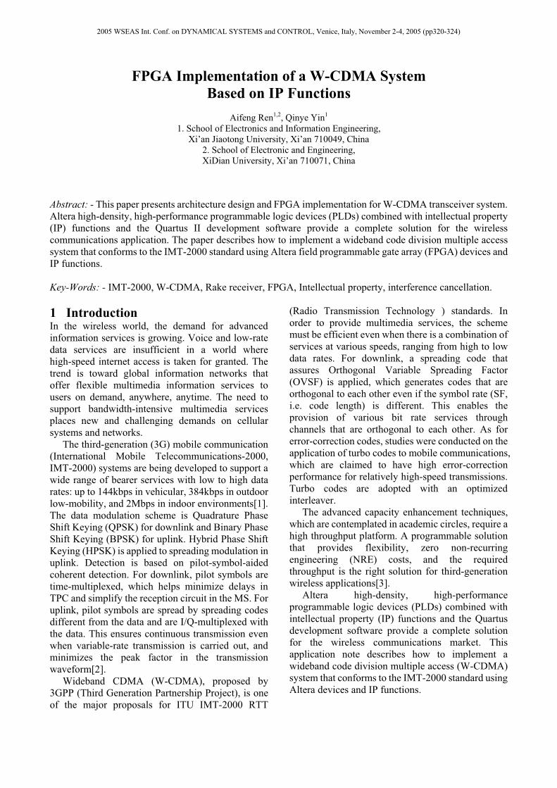
2.1 Transmitter Architecture Figure 1 shows the proposed digital architecture of a
downlink transmitter that supports the W-CDMA
standard.
CRCFEC
Encoder
Block
Interleaver
QPSK
ModulatorSpreading
Baseband
Transmit
Filter
DAC
OVSF Code
Generator
Data
To RF
Fig.1 W-CDMA transmitter digital architecture
To conform to the W-CDMA standard, cyclic
redundancy code (CRC) bits are added for detecting
block errors. This is followed by channel encoding
(Forward Error Correction, FEC) and interleaving.
By two layers of spreading code sequences, in-phase
and quadrature components in the phase plane
mapped following data modulation are spread across
the spectrum. To transmit a signal within the
specified bandwidth, the resulting chip data bits are
shaped using a pulse shaping filter. Then, the signal
goes through carrier modulation and up-conversion
to radio frequency (RF), and is then sent to the
antenna to be transmitted over the air.
The various block functions used in the
transmitter digital architecture, such as CRC checker,
FEC, Block interleaver, OVSF channelization codes,
spreading codes and QPSK modulator, are provided
in Altera MegaCore functions or IP functions, which
can implement these functions and therefore meets
the third-generation standard requirements.
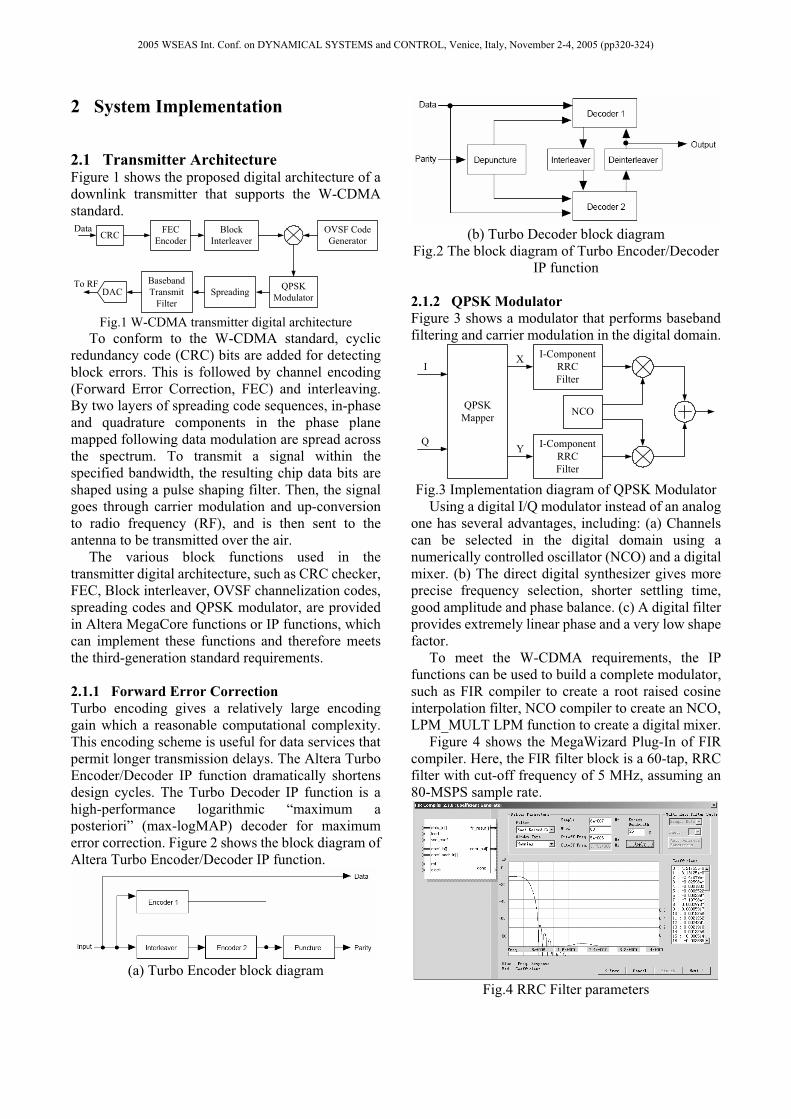
2.1.1 Forward Error Correction
Turbo encoding gives a relatively large encoding
gain which a reasonable computational complexity.
This encoding scheme is useful for data services that
permit longer transmission delays. The Altera Turbo
Encoder/Decoder IP function dramatically shortens
design cycles. The Turbo Decoder IP function is a
high-performance logarithmic “maximum a
posteriori” (max-logMAP) decoder for maximum
error correction. Figure 2 shows the block diagram of
Altera Turbo Encoder/Decoder IP function.
(a) Turbo Encoder block diagram
(b) Turbo Decoder block diagram
Fig.2 The block diagram of Turbo Encoder/Decoder
IP function
2.1.2 QPSK Modulator
Figure 3 shows a modulator that performs baseband
filtering and carrier modulation in the digital domain.
QPSK
Mapper
I-Component
RRC
Filter
I-Component
RRC
Filter
NCO
X
Y
I
Q
Fig.3 Implementation diagram of QPSK Modulator
Using a digital I/Q modulator instead of an analog
one has several advantages, including: (a) Channels
can be selected in the digital domain using a
numerically controlled oscillator (NCO) and a digital
mixer. (b) The direct digital synthesizer gives more
precise frequency selection, shorter settling time,
good amplitude and phase balance. (c) A digital filter
provides extremely linear phase and a very low shape
factor.
To meet the W-CDMA requirements, the IP
functions can be used to build a complete modulator,
such as FIR compiler to create a root raised cosine
interpolation filter, NCO compiler to create an NCO,
LPM_MULT LPM function to create a digital mixer.
Figure 4 shows the MegaWizard Plug-In of FIR
compiler. Here, the FIR filter block is a 60-tap, RRC
filter with cut-off frequency of 5 MHz, assuming an
80-MSPS sample rate.
Fig.4 RRC Filter parameters
2005 WSEAS Int. Conf. on DYNAMICAL SYSTEMS and CONTROL, Venice, Italy, November 2-4, 2005 (pp320-324)
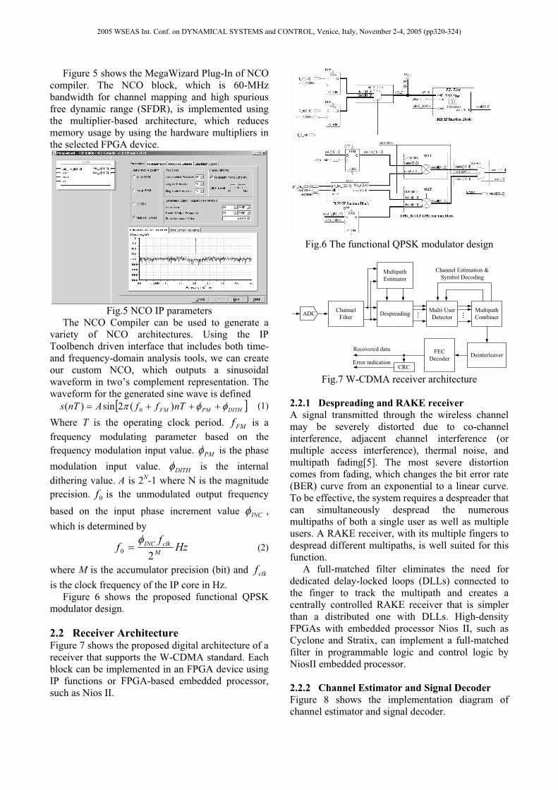
Figure 5 shows the MegaWizard Plug-In of NCO
compiler. The NCO block, which is 60-MHz
bandwidth for channel mapping and high spurious
free dynamic range (SFDR), is implemented using
the multiplier-based architecture, which reduces
memory usage by using the hardware multipliers in
the selected FPGA device.
Fig.5 NCO IP parameters
The NCO Compiler can be used to generate a
variety of NCO architectures. Using the IP
Toolbench driven interface that includes both time-
and frequency-domain analysis tools, we can create
our custom NCO, which outputs a sinusoidal
waveform in two’s complement representation. The
waveform for the generated sine wave is defined
DITHPMFM nTffAnTs )(2sin)( 0 (1)
Where T is the operating clock period. FMf is a
frequency modulating parameter based on the
frequency modulation input value. PM is the phase
modulation input value. DITH is the internal
dithering value. A is 2N-1 where N is the magnitude
precision. 0f is the unmodulated output frequency
based on the input phase increment value INC ,
which is determined by
Hzf
fM
clkINC
20 (2)
where M is the accumulator precision (bit) and clkf
is the clock frequency of the IP core in Hz.
Figure 6 shows the proposed functional QPSK
modulator design.
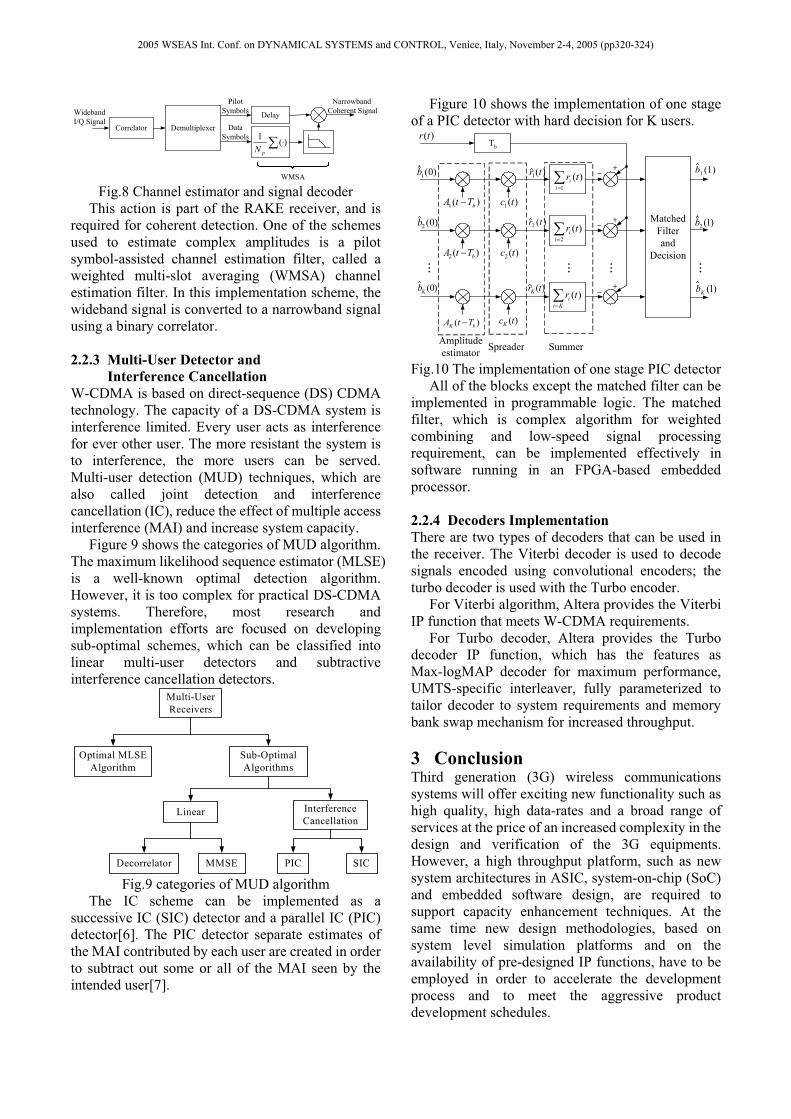
2.2 Receiver Architecture Figure 7 shows the proposed digital architecture of a
receiver that supports the W-CDMA standard. Each
block can be implemented in an FPGA device using
IP functions or FPGA-based embedded processor,
such as Nios II.
Fig.6 The functional QPSK modulator design
Channel
FilterADC Despreading
Multipath
Estimator
Multi-User
Detector
Multipath
Combiner
DeinterleaverFEC
Decoder
CRC
...
...
Recovered data
Error indication
Channel Estimation &
Symbol Decoding
Fig.7 W-CDMA receiver architecture
2.2.1 Despreading and RAKE receiver
A signal transmitted through the wireless channel
may be severely distorted due to co-channel
interference, adjacent channel interference (or
multiple access interference), thermal noise, and
multipath fading[5]. The most severe distortion
comes from fading, which changes the bit error rate
(BER) curve from an exponential to a linear curve.
To be effective, the system requires a despreader that
can simultaneously despread the numerous
multipaths of both a single user as well as multiple
users. A RAKE receiver, with its multiple fingers to
despread different multipaths, is well suited for this
function.
A full-matched filter eliminates the need for
dedicated delay-locked loops (DLLs) connected to
the finger to track the multipath and creates a
centrally controlled RAKE receiver that is simpler
than a distributed one with DLLs. High-density
FPGAs with embedded processor Nios II, such as
Cyclone and Stratix, can implement a full-matched
filter in programmable logic and control logic by
NiosII embedded processor.
2.2.2 Channel Estimator and Signal Decoder
Figure 8 shows the implementation diagram of
channel estimator and signal decoder.
2005 WSEAS Int. Conf. on DYNAMICAL SYSTEMS and CONTROL, Venice, Italy, November 2-4, 2005 (pp320-324)
Correlator Demultiplexer
Delay
)(1
pN
Wideband
I/Q Signal
Pilot
Symbols
Data
Symbols
Narrowband
Coherent Signal
WMSA
Fig.8 Channel estimator and signal decoder
This action is part of the RAKE receiver, and is
required for coherent detection. One of the schemes
used to estimate complex amplitudes is a pilot
symbol-assisted channel estimation filter, called a
weighted multi-slot averaging (WMSA) channel
estimation filter. In this implementation scheme, the
wideband signal is converted to a narrowband signal
using a binary correlator.
2.2.3 Multi-User Detector and
Interference Cancellation
W-CDMA is based on direct-sequence (DS) CDMA
technology. The capacity of a DS-CDMA system is
interference limited. Every user acts as interference
for ever other user. The more resistant the system is
to interference, the more users can be served.
Multi-user detection (MUD) techniques, which are
also called joint detection and interference
cancellation (IC), reduce the effect of multiple access
interference (MAI) and increase system capacity.
Figure 9 shows the categories of MUD algorithm.
The maximum likelihood sequence estimator (MLSE)
is a well-known optimal detection algorithm.
However, it is too complex for practical DS-CDMA
systems. Therefore, most research and
implementation efforts are focused on developing
sub-optimal schemes, which can be classified into
linear multi-user detectors and subtractive
interference cancellation detectors. Multi-User
Receivers
Optimal MLSE
Algorithm
Sub-Optimal
Algorithms
Linear Interference
Cancellation
Decorrelator MMSE PIC SIC
Fig.9 categories of MUD algorithm
The IC scheme can be implemented as a
successive IC (SIC) detector and a parallel IC (PIC)
detector[6]. The PIC detector separate estimates of
the MAI contributed by each user are created in order
to subtract out some or all of the MAI seen by the
intended user[7].
Figure 10 shows the implementation of one stage
of a PIC detector with hard decision for K users.
Tb
1
)(i
i tr
)(1 bTtA )(1 tc
)(1 tr
)(2 bTtA )(2 tc
)(2 tr
...
...
)( bK TtA )(tcK
)(trK
...
2
)(i
i tr
Ki
i tr )(
Matched
Filter
and
Decision
...
)0(1b
)0(2b
)0(Kb
)1(1b
)1(2b
)1(Kb
)(tr
Amplitude
estimatorSpreader Summer
Fig.10 The implementation of one stage PIC detector
All of the blocks except the matched filter can be
implemented in programmable logic. The matched
filter, which is complex algorithm for weighted
combining and low-speed signal processing
requirement, can be implemented effectively in
software running in an FPGA-based embedded
processor.
2.2.4 Decoders Implementation
There are two types of decoders that can be used in
the receiver. The Viterbi decoder is used to decode
signals encoded using convolutional encoders; the
turbo decoder is used with the Turbo encoder.
For Viterbi algorithm, Altera provides the Viterbi
IP function that meets W-CDMA requirements.
For Turbo decoder, Altera provides the Turbo
decoder IP function, which has the features as
Max-logMAP decoder for maximum performance,
UMTS-specific interleaver, fully parameterized to
tailor decoder to system requirements and memory
bank swap mechanism for increased throughput.
3 Conclusion Third generation (3G) wireless communications
systems will offer exciting new functionality such as
high quality, high data-rates and a broad range of
services at the price of an increased complexity in the
design and verification of the 3G equipments.
However, a high throughput platform, such as new
system architectures in ASIC, system-on-chip (SoC)
and embedded software design, are required to
support capacity enhancement techniques. At the
same time new design methodologies, based on
system level simulation platforms and on the
availability of pre-designed IP functions, have to be
employed in order to accelerate the development
process and to meet the aggressive product
development schedules.
2005 WSEAS Int. Conf. on DYNAMICAL SYSTEMS and CONTROL, Venice, Italy, November 2-4, 2005 (pp320-324)
We believe that the proposed architectures serve
as a solid foundation for future cost-effective
application-specific integrated circuit (ASIC)
implementation of the baseband processing circuit in
a W-CDMA systems.
References: [1] HP Ma, SH Hsu, and TD Chiueh, Design and
Implementation of an Uplink Baseband Receiver
for Wideband CDMA Communications, IEICE
Trans. On Fundamentals of Electronics,
Communications and Computer Sciences,
Vol.E85-A, No.12, 2002, pp. 2813-2821.
[2] T. Keiji, W-CDMA: Mobile Communications
System, John Wiley & Sons, 2002
[3] Altera AN129, Implementing a W-CDMA
System, 9. 2000, Ver.1.0
[4] D. Chris, FPGA Implementation of Carrier
Synchronization for QAM Receivers, Journal of
VLSI Signal Processing, Vol. 36, 2004, pp.57-71.
[5] G. C. Kim, Maximum Ratio Combining for a
WCDMA Rake Receiver, Freescal
Semiconductor Application Note. Rev.2, 11,
2004.
[6] S. Ivan, I. P. Klaus, K. E. Troels, M. H. Jack,
Implementation aspects for successive
interference cancellation in DS/CDMA systems,
Wireless Networks, Vol.4, 1998. pp. 447-452.
[7] A. Amr, E. Sald, Implementation of Multi-User
Detection for DS-CDMA Communications,
NRSC 2005, March 15-17, 2005 Cairo-Egypt.
[8] S. Moshavi, Multi-user detection for DS-CDMA
Communications, IEEE Communications
Magazine, Vol.34, 8. 1996, pp.124-136.
2005 WSEAS Int. Conf. on DYNAMICAL SYSTEMS and CONTROL, Venice, Italy, November 2-4, 2005 (pp320-324)


