TC3299APreliminary Data Sheet
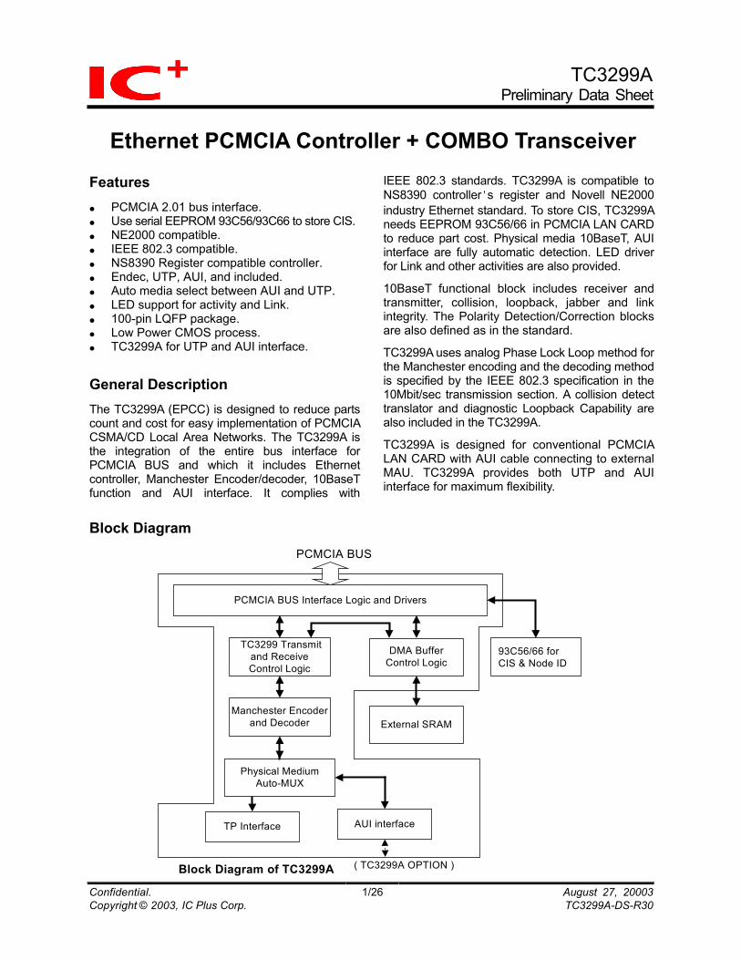
PCMCIA BUS Interface Logic and Drivers
PCMCIA BUS
TC3299 Transmitand ReceiveControl Logic
External SRAM
DMA BufferControl Logic
Manchester Encoderand Decoder
AUI interfaceTP Interface
Physical MediumAuto-MUX
Block Diagram of TC3299A
93C56/66 forCIS & Node ID
( TC3299A OPTION )
Ethernet PCMCIA Controller + COMBO Transceiver
Features
1/26 August 27, 20003Copyright © 2003, IC Plus Corp. TC3299A-DS-R30
PCMCIA 2.01 bus interface. Use serial EEPROM 93C56/93C66 to store CIS. NE2000 compatible. IEEE 802.3 compatible. NS8390 Register compatible controller. Endec, UTP, AUI, and included. Auto media select between AUI and UTP. LED support for activity and Link. 100-pin LQFP package. Low Power CMOS process. TC3299A for UTP and AUI interface.
General Description The TC3299A (EPCC) is designed to reduce parts count and cost for easy implementation of PCMCIA CSMA/CD Local Area Networks. The TC3299A is the integration of the entire bus interface for PCMCIA BUS and which it includes Ethernet controller, Manchester Encoder/decoder, 10BaseT function and AUI interface. It complies with
IEEE 802.3 standards. TC3299A is compatible to NS8390 controller's register and Novell NE2000 industry Ethernet standard. To store CIS, TC3299A needs EEPROM 93C56/66 in PCMCIA LAN CARD to reduce part cost. Physical media 10BaseT, AUI interface are fully automatic detection. LED driver for Link and other activities are also provided.
TC3299A is designed for conventional PCMCIA LAN CARD with AUI cable connecting to external MAU. TC3299A provides both UTP and AUI interface for maximum flexibility.
10BaseT functional block includes receiver and transmitter, collision, loopback, jabber and link integrity. The Polarity Detection/Correction blocks are also defined as in the standard.
TC3299A uses analog Phase Lock Loop method for the Manchester encoding and the decoding method is specified by the IEEE 802.3 specification in the 10Mbit/sec transmission section. A collision detect translator and diagnostic Loopback Capability are also included in the TC3299A.
Block Diagram
Confidential.
TC3299APreliminary Data Sheet
Table Of Contents Features ..............................................................................................................................................................1General Description............................................................................................................................................1Block Diagram.....................................................................................................................................................1Table Of Contents ...............................................................................................................................................2Pin Configuration ................................................................................................................................................31 Pin Description ............................................................................................................................................42 Functional Description ................................................................................................................................7
2.1 Power On Configuration....................................................................................................... 93 Configuration Registers ............................................................................................................................11
3.1 EPCC Core Registers ........................................................................................................ 124 Absolute Maximum Ratings......................................................................................................................255 Standard Test Conditions..........................................................................................................................256 D.C. Characteristics................................................................................................................................257 Physical Dimensions.................................................................................................................................26
Confidential. 2/26 August 27, 20003Copyright © 2003, IC Plus Corp. TC3299A-DS-R30
TC3299APreliminary Data Sheet
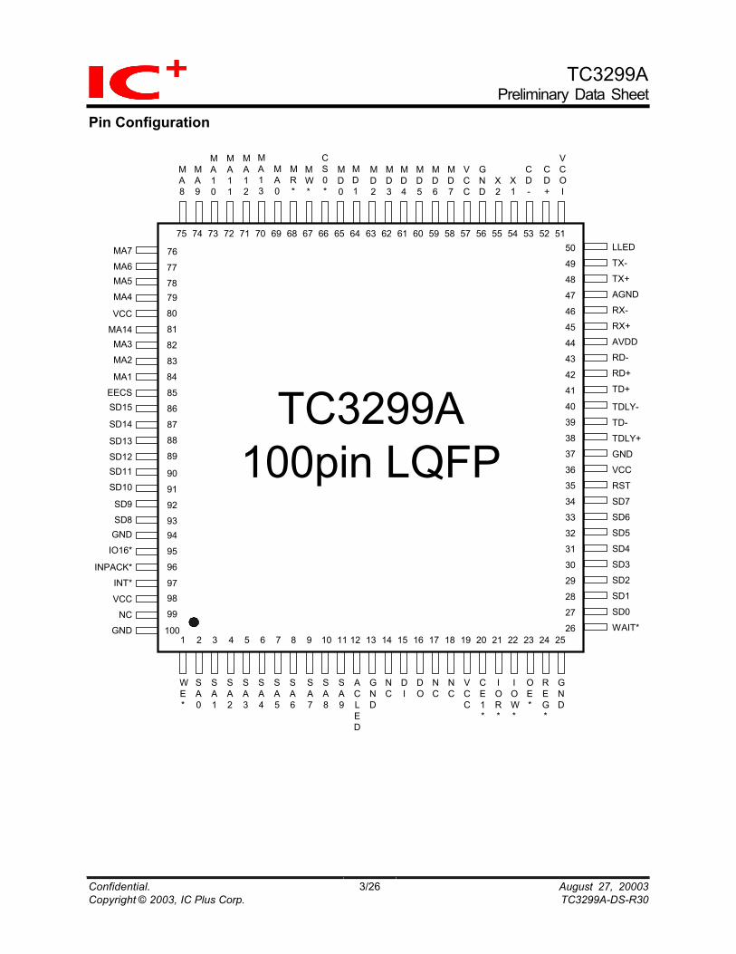
Pin Configuration
1 2 3 4 5 6 7 8 9 10 11 12 13 14 15 16 17 18 19 20 21 22 23 24 25
81
82
8384
85
86
87
88
89
90
91
92
9394
95
96
9798
99
100
WE*
SA0
SA1
SA2
SA3
SA4
SA5
SA6
SA7
SA8
SA9
ACLED
GND
NC
DI
DO
NC
NC
VCC
CE1*
IOR*
IOW*
OE*
REG*
GND
MA14MA3
MA2
MA1
EECSSD15
SD14
SD13SD12SD11
SD10
SD9SD8
GND
IO16*
INPACK*
INT*
VCC
NCGND
51525354555657585960616263646566676869707172737475
VCOI
CD+
26
27
28
29
30
31
32
33
34
35
36
37
38
39
40
41
42
43
44
45
WAIT*
SD0
SD1
SD2SD3
SD4
SD5
SD6SD7
RST
VCC
GNDTDLY+
TD-
TDLY-
TD+
RD+
RD-AVDD
RX+46
47
48
49
50
RX-
AGNDTX+
TX-
LLED76
777879
80
MA7
MA6MA5
MA4
VCC
TC3299A100pin LQFP
CD-
X1
MD1
MA12
MW*
MA10
MA9
MA8
MD0
CS0*
MR*
MA0
MA13
MA11
X2
GND
VCC
MD7
MD6
MD5
MD4
MD3
MD2
Confidential. 3/26 August 27, 20003Copyright © 2003, IC Plus Corp. TC3299A-DS-R30
TC3299APreliminary Data Sheet
1 Pin Description
Pin No. Symbol I/O Description ISA Bus Interface Pins 2-11 SA0-SA9 I These address signal lines of PCMCIA Bus are used to select a
register to be read or written and attribute memory enable. 27-34 93-86
SD0-SD7 SD8-SD15
I/O I/O
Register Access, with DMA inactive, SD0-SD7 pins are used toread/write register data. SD8-SD15 pins are invalid during this state.Remote DMA Bus Cycle, SD0-SD15 pins contain packet data.Direction of transfer is depended on Remote read/write.
35 RST I Reset pin. RST is active high and placed EPCC in a reset modeimmediately. During falling edge, the EPCC controller loads theconfiguration from MD0-7, MA0-13.
26 WAIT* O This pin is set low to insert wait states during Remote DMA transfer. 24 REG* I REG* is an active low input used to determine whether a lost access is
to Attribute memory (The first 1K) or to common memory (above 1K). If REG* is set to low the access is to attribute memory, while REG* isset to high the access is to common memory. REG* is also assertedlow for all accesses to the TC3299A's IO Registers.
21 IOR* I Read Strobe: Strobe from host to read internal registers or RemoteDMA read.
22 IOW* I Write Strobe: Strobe from host to write internal registers or RemoteDMA write.
23 OE* I Host memory read strobe. The attribute memory can be read whenOE* and REG* are both at low state. While for Common memory to be accessed, OE* should be set to lowstate and REG* should set to high state. OE* REG* Attribute Memory Low Low Common Memory Low High
1 WE* I Host memory write strobe. After Power reset, if TC3299A is configuredto memory write enable, then 2 types of memories are written asdefined below: WE* REG* Attribute Memory Low Low Common Memory Low High
96 INPACK* O Active low signal, asserted if the host access TC3299A internalregister or Remote DMA read cycle.
95 IO16* O IO16* is driven by EPCC to support host 16 bits access cycle. 97 INT* O Interrupt:Indicates that the EPCC requires host attention after
reception, transmission or completion of DMA transfer. 20 CE1* I Card enable 1, are active low signals driven by the host. These signals
provide a card select based on an address decode (decode by thehost).
Confidential. 4/26 August 27, 20003Copyright © 2003, IC Plus Corp. TC3299A-DS-R30
TC3299APreliminary Data Sheet
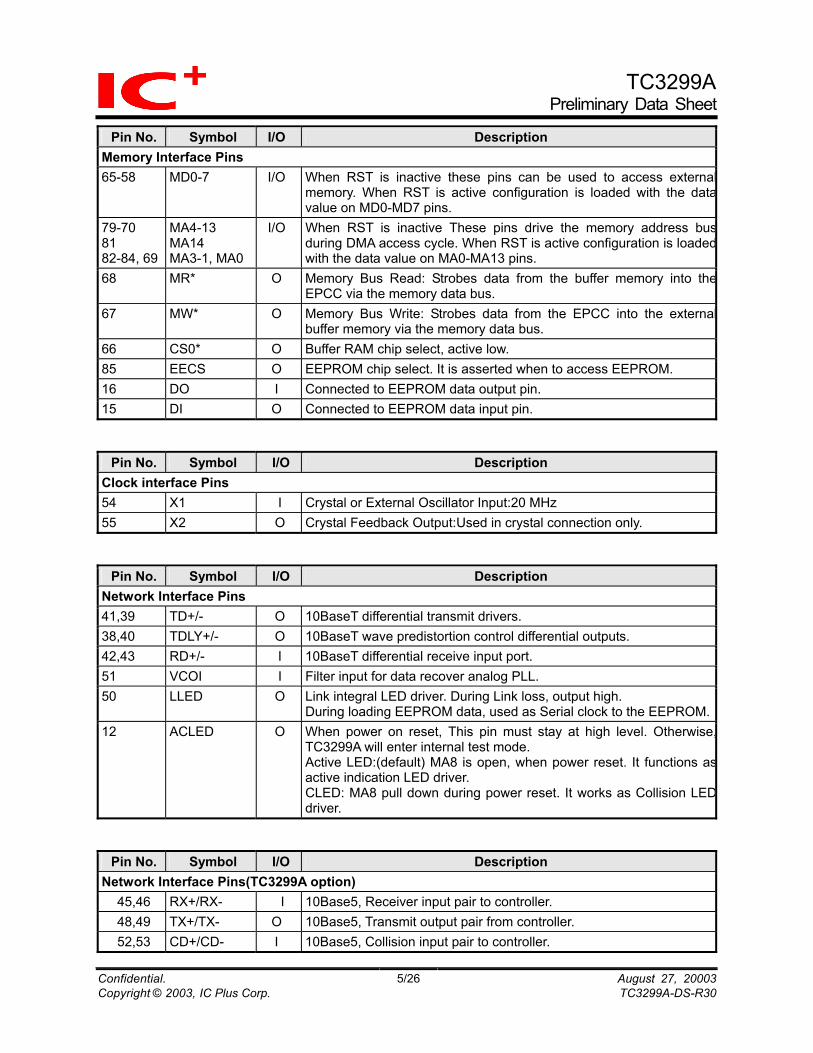
Pin No. Symbol I/O Description Memory Interface Pins 65-58 MD0-7 I/O When RST is inactive these pins can be used to access external
memory. When RST is active configuration is loaded with the datavalue on MD0-MD7 pins.
79-70 81 82-84, 69
MA4-13 MA14 MA3-1, MA0
I/O When RST is inactive These pins drive the memory address busduring DMA access cycle. When RST is active configuration is loadedwith the data value on MA0-MA13 pins.
68 MR* O Memory Bus Read: Strobes data from the buffer memory into theEPCC via the memory data bus.
67 MW* O Memory Bus Write: Strobes data from the EPCC into the externalbuffer memory via the memory data bus.
66 CS0* O Buffer RAM chip select, active low. 85 EECS O EEPROM chip select. It is asserted when to access EEPROM. 16 DO I Connected to EEPROM data output pin. 15 DI O Connected to EEPROM data input pin.
Pin No. Symbol I/O Description Clock interface Pins 54 X1 I Crystal or External Oscillator Input:20 MHz 55 X2 O Crystal Feedback Output:Used in crystal connection only.
Pin No. Symbol I/O Description
Network Interface Pins 41,39 TD+/- O 10BaseT differential transmit drivers. 38,40 TDLY+/- O 10BaseT wave predistortion control differential outputs. 42,43 RD+/- I 10BaseT differential receive input port. 51 VCOI I Filter input for data recover analog PLL. 50 LLED O Link integral LED driver. During Link loss, output high.
During loading EEPROM data, used as Serial clock to the EEPROM.12 ACLED O When power on reset, This pin must stay at high level. Otherwise,
TC3299A will enter internal test mode. Active LED:(default) MA8 is open, when power reset. It functions asactive indication LED driver. CLED: MA8 pull down during power reset. It works as Collision LEDdriver.
Pin No. Symbol I/O Description Network Interface Pins(TC3299A option)
45,46 RX+/RX- I 10Base5, Receiver input pair to controller. 48,49 TX+/TX- O 10Base5, Transmit output pair from controller. 52,53 CD+/CD- I 10Base5, Collision input pair to controller.
Confidential. 5/26 August 27, 20003Copyright © 2003, IC Plus Corp. TC3299A-DS-R30
TC3299APreliminary Data Sheet
Pin No. Symbol I/O Description
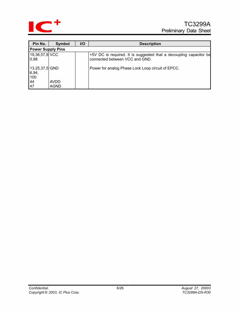
Power Supply Pins 19,36,57,80,98 13,25,37,56,94, 100 44 47
VCC GND AVDD AGND
+5V DC is required. It is suggested that a decoupling capacitor beconnected between VCC and GND. Power for analog Phase Lock Loop circuit of EPCC.
Confidential. 6/26 August 27, 20003Copyright © 2003, IC Plus Corp. TC3299A-DS-R30
TC3299APreliminary Data Sheet
2 Functional Description The EPCC controller is a highly integrated jumperless configurable Ethernet controller. It integrates the function of the following blocks: TC3299A Ethernet Controller Core and Media Access Control logic. 1. PCMCIA 2.0 Bus interface containing all logics require to connect the TC3299A core to a packet
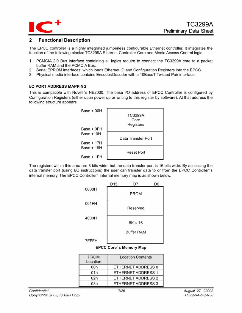
buffer RAM and the PCMCIA Bus. 2. Serial EPROM interfaces, which loads Ethernet ID and Configuration Registers into the EPCC. 3. Physical media interface contains Encoder/Decoder with a 10BaseT Twisted Pair interface. I/O PORT ADDRESS MAPPING This is compatible with Novell's NE2000. The base I/O address of EPCC Controller is configured by Configuration Registers (either upon power up or writing to this register by software). At that address the following structure appears.
Base + 00H Base + 0FH
TC3299A
Core Registers
Base +10H Base + 17H
Data Transfer Port
Base + 18H Base + 1FH
Reset Port
The registers within this area are 8 bits wide, but the data transfer port is 16 bits wide. By accessing the data transfer port (using I/O instructions) the user can transfer data to or from the EPCC Controller's internal memory. The EPCC Controller' internal memory map is as shown below.
D15 D7 D0 0000H
PROM
001FH Reserved
4000H
7FFFH
8K × 16
Buffer RAM
EPCC Core's Memory Map
PROM Location
Location Contents
00h ETHERNET ADDRESS 0 01h ETHERNET ADDRESS 1 02h ETHERNET ADDRESS 2 03h ETHERNET ADDRESS 3
Confidential. 7/26 August 27, 20003Copyright © 2003, IC Plus Corp. TC3299A-DS-R30
TC3299APreliminary Data Sheet
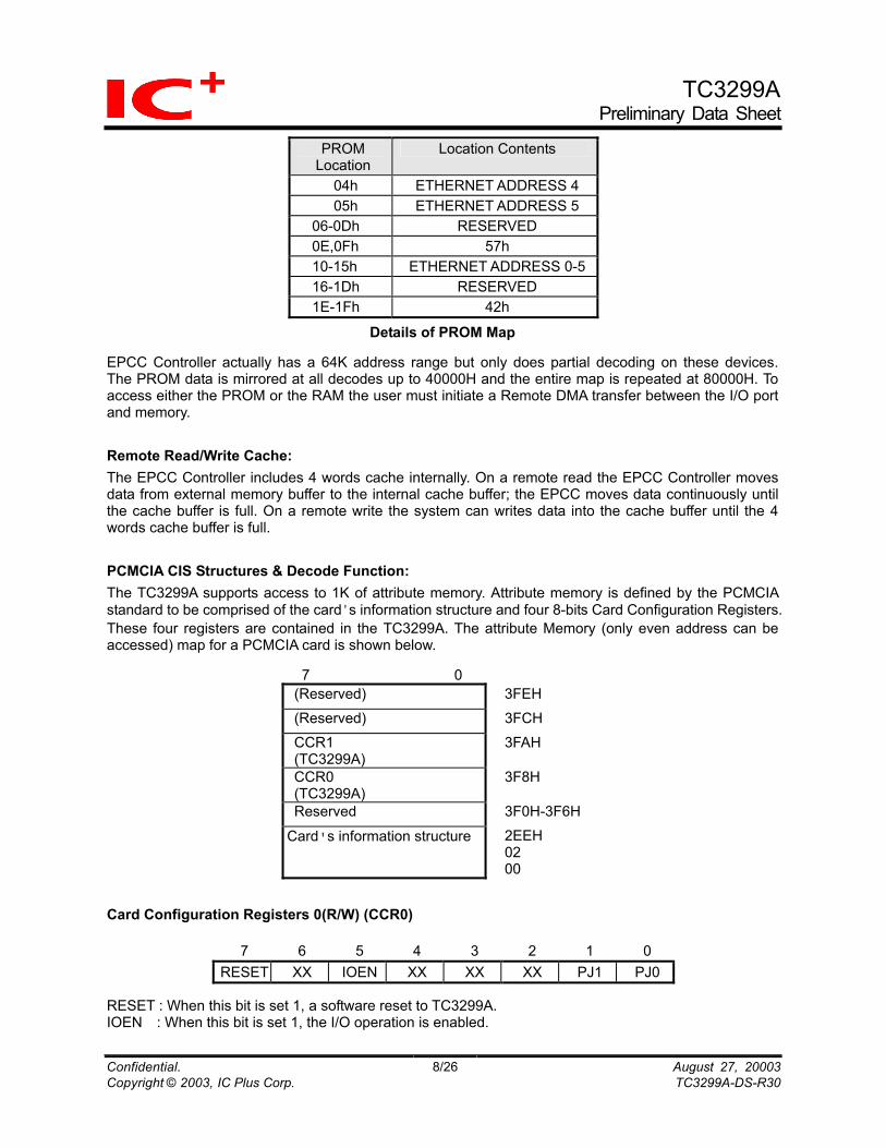
PROM Location
Location Contents
04h ETHERNET ADDRESS 4 05h ETHERNET ADDRESS 5 06-0Dh RESERVED 0E,0Fh 57h 10-15h ETHERNET ADDRESS 0-5 16-1Dh RESERVED 1E-1Fh 42h
Details of PROM Map EPCC Controller actually has a 64K address range but only does partial decoding on these devices. The PROM data is mirrored at all decodes up to 40000H and the entire map is repeated at 80000H. To access either the PROM or the RAM the user must initiate a Remote DMA transfer between the I/O port and memory. Remote Read/Write Cache: The EPCC Controller includes 4 words cache internally. On a remote read the EPCC Controller moves data from external memory buffer to the internal cache buffer; the EPCC moves data continuously until the cache buffer is full. On a remote write the system can writes data into the cache buffer until the 4 words cache buffer is full. PCMCIA CIS Structures & Decode Function: The TC3299A supports access to 1K of attribute memory. Attribute memory is defined by the PCMCIA standard to be comprised of the card's information structure and four 8-bits Card Configuration Registers. These four registers are contained in the TC3299A. The attribute Memory (only even address can be accessed) map for a PCMCIA card is shown below. 7 0
(Reserved) 3FEH (Reserved) 3FCH CCR1 (TC3299A)
3FAH
CCR0 (TC3299A)
3F8H
Reserved 3F0H-3F6H
Card's information structure 2EEH 02 00
Card Configuration Registers 0(R/W) (CCR0)
7 6 5 4 3 2 1 0 RESET XX IOEN XX XX XX PJ1 PJ0
RESET : When this bit is set 1, a software reset to TC3299A. IOEN : When this bit is set 1, the I/O operation is enabled.
Confidential. 8/26 August 27, 20003Copyright © 2003, IC Plus Corp. TC3299A-DS-R30
TC3299APreliminary Data Sheet
PJ1,0 : If MA12 isn't pulled low during power on reset, despite of the value of PJ1,0, TC3299A response to I/O access at the I/O base address 300h, 320h, 340h, 360h. otherwise, I/O base Map as below:
PJ1 PJ0 I/O base Map 0 0 300h 0 1 320h 1 0 340h 1 1 360h PJ1,0 : Reserved Configuration Registers 1 ® (CCR1)
7 6 5 4 3 2 1 0 XX XX XX XX XX XX IREQ XX
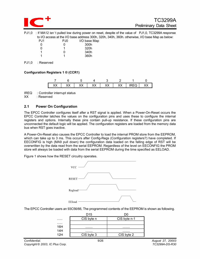
IREQ : Controller interrupt status XX : Reserved 2.1 Power On Configuration The EPCC Controller configures itself after a RST signal is applied. When a Power-On-Reset occurs the EPCC Controller latches the values on the configuration pins and uses these to configure the internal registers and options. Internally these pins contain pull-up resistance. If these configuration pins are unconnected the default logic will be applied. The configuration registers are loaded from the memory data bus when RST goes inactive. A Power-On-Reset also causes the EPCC Controller to load the internal PROM store from the EEPROM, which can take up to 3 ms. This occurs after Config-Regs (Configuration registers?) have completed. If EECONFIG is high (MA9 pull down) the configuration data loaded on the falling edge of RST will be overwritten by the data read from the serial EEPROM. Regardless of the level on EECONFIG the PROM store will always be loaded with data from the serial EEPROM during the time specified as EELOAD. Figure 1 shows how the RESET circuitry operates.
VCC
RESET
Regload
EEload The EPCC Controller users an 93C56/66, The programmed contents of the EEPROM is shown as following.
D15 D0 ...... CIS byte n CIS byte n-1 ...... 16H ........ ........ 14H ........ ........ 12H CIS byte 3 CIS byte 2
Confidential. 9/26 August 27, 20003Copyright © 2003, IC Plus Corp. TC3299A-DS-R30
TC3299APreliminary Data Sheet
D15 D0 10H CIS byte 1 CIS byte 0 0FH Not Used Config. C 0EH Config. B Config. A Reserved Reserved 08H 42H 42H 07H 57H 57H 04H Reserved Reserved 03H
Reserved bit (0) : 8 bit enable bit (7:1) : Reserved
02H E'net Address 5 E'net Address 4 01H E'net Address 3 E'net Address 2 00H E'net Address 1 E'net Address 0
EEPROM Programming Map
**03H bit(0):If MA11 is pulled low during power on reset and this bit is set high. TC3299A can work at NE2000's 8-bit mode. Storing and Loading Configuration from EEPROM: If the EECONFIG is set high (MA9 pull low) during boot up, the EPCC Controller's configuration is determined by the EEPROM, before the PROM data is read The configuration data is stored within the address 0EH of the EEPROM's address space. Configuration Register A and B are located in the address 0EH. To write this configuration into the EEPROM, The user can program register in EPCC's address 02H of page 3. This operation will work regardless of the level on EECONFIG.
Confidential. 10/26 August 27, 20003Copyright © 2003, IC Plus Corp. TC3299A-DS-R30
TC3299APreliminary Data Sheet
3 Configuration Registers Configuration Register A (R/W) To prevent any accidental write of this register, it is ”hidden” behind a previously unused register. Register 0AH in the EPCC Controller's Page 0 of registers was previously reserved on a read. Now Configuration Register A can be read at that address and can be written to by following a read to 0AH with a write to 0AH. If any other ENCC Controller register accesses take place between the read and the write then the write to 0AH will access the Remote Byte Count Register 0.
7 6 5 4 3 2 1 0 XX FREAD XX XX XX XX XX XX
FREAD :The ENCC Controller supports 4 words Remote DMA read/write cache. When this bit is set
high,Remote DMA cache control will be enabled. XX :Reserved Configuration Register B (R/W) To prevent any accidental write of this register, it is ”hidden” behind a previously unused register. Register 0BH in the EPCC Controller's Page 0 of registers was previously reserved on a read. Now Configuration Register B can be read at that address and can be written to by following a read to 0BH with a write to 0BH. If any other ENCC Controller register accesses take place between the read and the write then the write to 0BH will access the Remote Byte Count Register 1.
7 6 5 4 3 2 1 0
XX LINK XX XX IO16CONGDLINK PHYS1 PHYS0 PHYS1,0 : PHYSICAL LAYER INTERFACE 0 0 AUTO DETECT 0 1 Reserved 1 0 10Base5 1 1 10BaseT
In auto detect mode. For TC3299A, MA10 open for 10BaseT or 10Base5 auto-detect. GDLINK : When this bit is high, to disable link test pulse generation and integrity checking. IO16CON : When this bit is set high the Controller generates IO16* after REG* and CE1* active. If low
this output is generated only on address decode. LINK : When this bit is high, link test integrity checking is Goood. Otherwise, indicate link signal Loss. XX : Reserved. Configuration Register C Can be load data from EEPROM only
7 6 5 4 3 2 1 0 XX XX XX XX XX XX CRDASEL XX
CRDASEL : When this bit is high. CRDA0, CRDA1 increasing address control by internal cache
state machine. Confidential. 11/26 August 27, 20003Copyright © 2003, IC Plus Corp. TC3299A-DS-R30
TC3299APreliminary Data Sheet
When this bit is low, CRDA0, CRDA1 increasing address control by remote read command. XX : Reserved.
Hardware Configuration These functions are configured during a power on RESET. EECFG(MA9) : MA9 should be pulled down to enable CFGA and CFGB load from EEPROM. AUICB(MA10) : In media physic auto detect mode. It should be opened for TC3299A. ENG8(MA11) : If MA11 is pull down and EEPROM 03H bit(0) is setting high, EPCC can work at NE2000 8
bit mode. Otherwise it will work at 16-bit mode. IOSP(MA12) : If MA12 is pull down, enable I/O base 300H,320H,340H, and 360H separately. If MA12 is
not pulled low, despite of the value of PJ1, 0, TC3299A responses to I/O access at the I/O base address 300h, 320h, 340h, and 360h.
DCD5BIT(MA13) : Regardless of MA12 setting, once MA13 is pulled down, TC3299A only decodes input address SA4 - SA0 and can only work at I/O Base address.
Programming Register (R/W) The EPCC Controller enable software (driver) programming EEPROM or testing interrupt signal through this register directly. It is located at EPCC's core register Page3 base+02H.
7 6 5 4 3 2 1 0 EESEL XX XX READ CS SK DI DO(r) ATTRDIS
EESEL,CS,SK,DI,DO : The software can read or program serial EEPROM directly through these pins.
EESEL should be set high before starting the EEPROM read/write. READ : EPCC can reload CFGA,CFGB and internal PROM if this bit is set high. When
reload state is completed, READ will be cleared to low. ATTRDIS : Attribute and common memory access will be disable if it is programmed to high. NOTE : DO : read only
ATTRDIS : write only 3.1 EPCC Core Registers All registers are 8-bit wide and mapped into two pages which are selected in the Command Registers (PS0,PS1). Pins A0-A3 are used to address registers within each page. Page 0 register are those registers which are commonly accessed during EPCC Controller operation while Page 1 registers are used primarily for initialization. The registers are partitioned to avoid having to perform two read/write cycles to access commonly used registers. Register Assignments:
A0-A3 RD WR Page 0 Address Assignments (PS1=0,PS0=0)
00H Command (CR) Command (CR) 01H Current Local DMA
Address 0 (CLDA0) Page Start Register (PSTART)
02H Current Local DMA Address 1 (CLDA1)
Page Stop Register (PSTOP)
03H Boundary Pointer (BNRY)
Boundary Pointer (BNRY)
Confidential. 12/26 August 27, 20003Copyright © 2003, IC Plus Corp. TC3299A-DS-R30
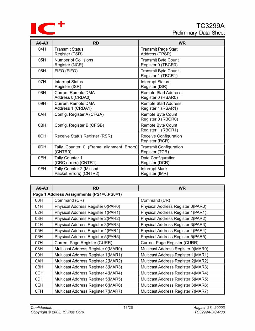
TC3299APreliminary Data Sheet
A0-A3 RD WR 04H Transmit Status
Register (TSR) Transmit Page Start Address (TPSR)
05H Number of Collisions Register (NCR)
Transmit Byte Count Register 0 (TBCR0)
06H FIFO (FIFO)
Transmit Byte Count Register 1 (TBCR1)
07H Interrupt Status Register (ISR)
Interrupt Status Register (ISR)
08H Current Remote DMA Address 0(CRDA0)
Remote Start Address Register 0 (RSAR0)
09H Current Remote DMA Address 1 (CRDA1)
Remote Start Address Register 1 (RSAR1)
0AH Config. Register A (CFGA)
Remote Byte Count Register 0 (RBCR0)
0BH Config. Register B (CFGB)
Remote Byte Count Register 1 (RBCR1)
0CH Receive Status Register (RSR)
Receive Configuration Register (RCR)
0DH Tally Counter 0 (Frame alignment Errors)(CNTR0)
Transmit Configuration Register (TCR)
0EH Tally Counter 1 (CRC errors) (CNTR1)
Data Configuration Register (DCR)
0FH Tally Counter 2 (Missed Packet Errors) (CNTR2)
Interrupt Mask Register (IMR)
A0-A3 RD WR Page 1 Address Assignments (PS1=0,PS0=1) 00H Command (CR) Command (CR) 01H Physical Address Register 0(PAR0) Physical Address Register 0(PAR0) 02H Physical Address Register 1(PAR1) Physical Address Register 1(PAR1) 03H Physical Address Register 2(PAR2) Physical Address Register 2(PAR2) 04H Physical Address Register 3(PAR3) Physical Address Register 3(PAR3) 05H Physical Address Register 4(PAR4) Physical Address Register 4(PAR4) 06H Physical Address Register 5(PAR5) Physical Address Register 5(PAR5) 07H Current Page Register (CURR) Current Page Register (CURR) 08H Multicast Address Register 0(MAR0) Multicast Address Register 0(MAR0) 09H Multicast Address Register 1(MAR1) Multicast Address Register 1(MAR1) 0AH Multicast Address Register 2(MAR2) Multicast Address Register 2(MAR2) 0BH Multicast Address Register 3(MAR3) Multicast Address Register 3(MAR3) 0CH Multicast Address Register 4(MAR4) Multicast Address Register 4(MAR4) 0DH Multicast Address Register 5(MAR5) Multicast Address Register 5(MAR5) 0EH Multicast Address Register 6(MAR6) Multicast Address Register 6(MAR6) 0FH Multicast Address Register 7(MAR7) Multicast Address Register 7(MAR7)
Confidential. 13/26 August 27, 20003Copyright © 2003, IC Plus Corp. TC3299A-DS-R30
TC3299APreliminary Data Sheet
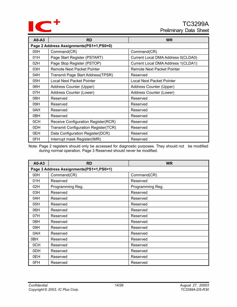
A0-A3 RD WR Page 2 Address Assignments(PS1=1,PS0=0) 00H Command(CR) Command(CR) 01H Page Start Register (PSTART) Current Local DMA Address 0(CLDA0) 02H Page Stop Register (PSTOP) Current Local DMA Address 1(CLDA1) 03H Remote Next Packet Pointer Remote Next Packet Pointer 04H Transmit Page Start Address(TPSR) Reserved 05H Local Next Packet Pointer Local Next Packet Pointer 06H Address Counter (Upper) Address Counter (Upper) 07H Address Counter (Lower) Address Counter (Lower) 08H Reserved Reserved 09H Reserved Reserved 0AH Reserved Reserved 0BH Reserved Reserved 0CH Receive Configuration Register(RCR) Reserved 0DH Transmit Configuration Register(TCR) Reserved 0EH Data Configuration Register(DCR) Reserved 0FH Interrupt mask Register(IMR) Reserved
Note: Page 2 registers should only be accessed for diagnostic purposes. They should not be modified during normal operation. Page 3 Reserved should never be modified.
A0-A3 RD WR Page 3 Address Assignments(PS1=1,PS0=1) 00H Command(CR) Command(CR) 01H Reserved Reserved 02H Programming Reg. Programming Reg. 03H Reserved Reserved 04H Reserved Reserved 05H Reserved Reserved 06H Reserved Reserved 07H Reserved Reserved 08H Reserved Reserved 09H Reserved Reserved 0AH Reserved Reserved 0BH Reserved Reserved 0CH Reserved Reserved 0DH Reserved Reserved 0EH Reserved Reserved 0FH Reserved Reserved
Confidential. 14/26 August 27, 20003Copyright © 2003, IC Plus Corp. TC3299A-DS-R30
TC3299APreliminary Data Sheet
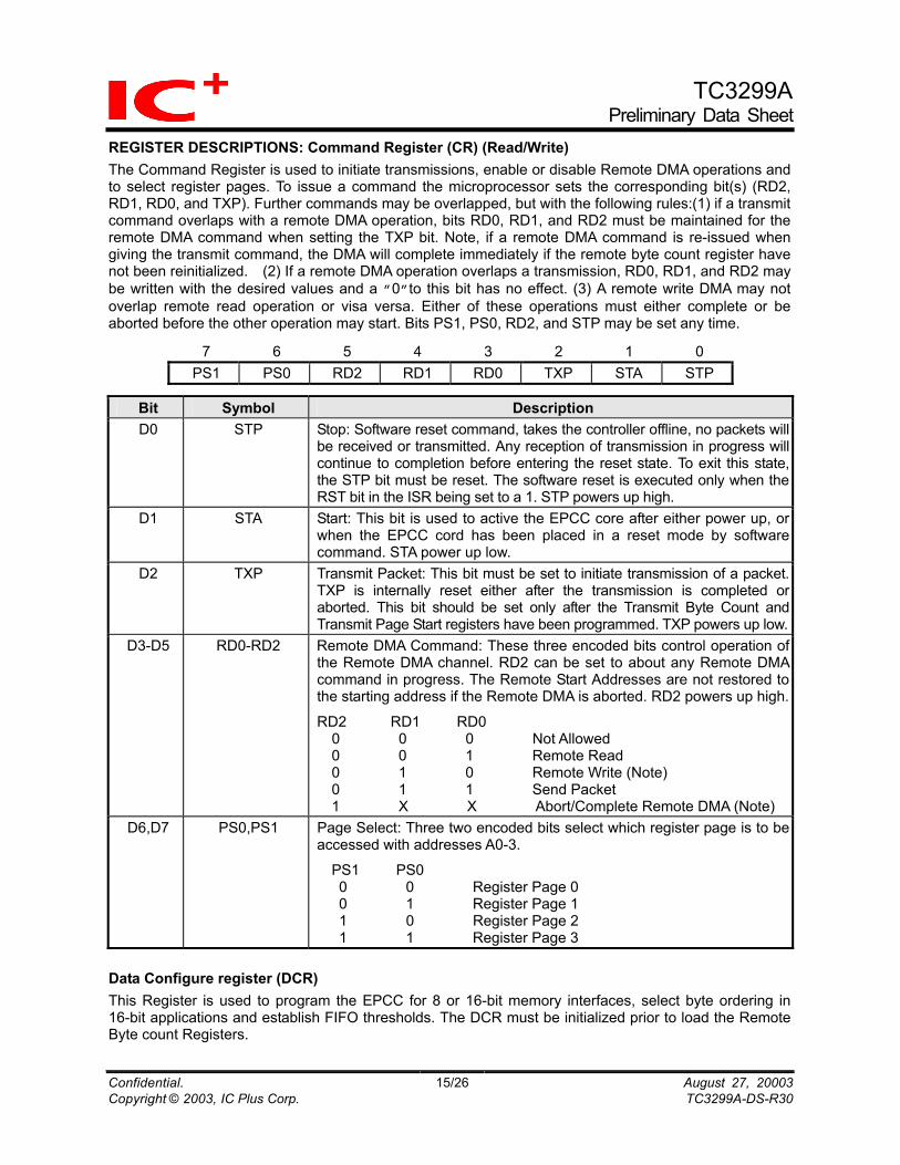
REGISTER DESCRIPTIONS: Command Register (CR) (Read/Write) The Command Register is used to initiate transmissions, enable or disable Remote DMA operations and to select register pages. To issue a command the microprocessor sets the corresponding bit(s) (RD2, RD1, RD0, and TXP). Further commands may be overlapped, but with the following rules:(1) if a transmit command overlaps with a remote DMA operation, bits RD0, RD1, and RD2 must be maintained for the remote DMA command when setting the TXP bit. Note, if a remote DMA command is re-issued when giving the transmit command, the DMA will complete immediately if the remote byte count register have not been reinitialized. (2) If a remote DMA operation overlaps a transmission, RD0, RD1, and RD2 may be written with the desired values and a ”0”to this bit has no effect. (3) A remote write DMA may not overlap remote read operation or visa versa. Either of these operations must either complete or be aborted before the other operation may start. Bits PS1, PS0, RD2, and STP may be set any time.
7 6 5 4 3 2 1 0 PS1 PS0 RD2 RD1 RD0 TXP STA STP
Bit Symbol Description D0 STP Stop: Software reset command, takes the controller offline, no packets will
be received or transmitted. Any reception of transmission in progress will continue to completion before entering the reset state. To exit this state, the STP bit must be reset. The software reset is executed only when the RST bit in the ISR being set to a 1. STP powers up high.
D1 STA Start: This bit is used to active the EPCC core after either power up, or when the EPCC cord has been placed in a reset mode by software command. STA power up low.
D2 TXP Transmit Packet: This bit must be set to initiate transmission of a packet. TXP is internally reset either after the transmission is completed or aborted. This bit should be set only after the Transmit Byte Count and Transmit Page Start registers have been programmed. TXP powers up low.
D3-D5 RD0-RD2 Remote DMA Command: These three encoded bits control operation of the Remote DMA channel. RD2 can be set to about any Remote DMA command in progress. The Remote Start Addresses are not restored to the starting address if the Remote DMA is aborted. RD2 powers up high.
RD2 RD1 RD0 0 0 0 Not Allowed
0 0 1 Remote Read 0 1 0 Remote Write (Note) 0 1 1 Send Packet 1 X X Abort/Complete Remote DMA (Note)
D6,D7 PS0,PS1 Page Select: Three two encoded bits select which register page is to be accessed with addresses A0-3.
PS1 PS0 0 0 Register Page 0 0 1 Register Page 1
1 0 Register Page 2 1 1 Register Page 3
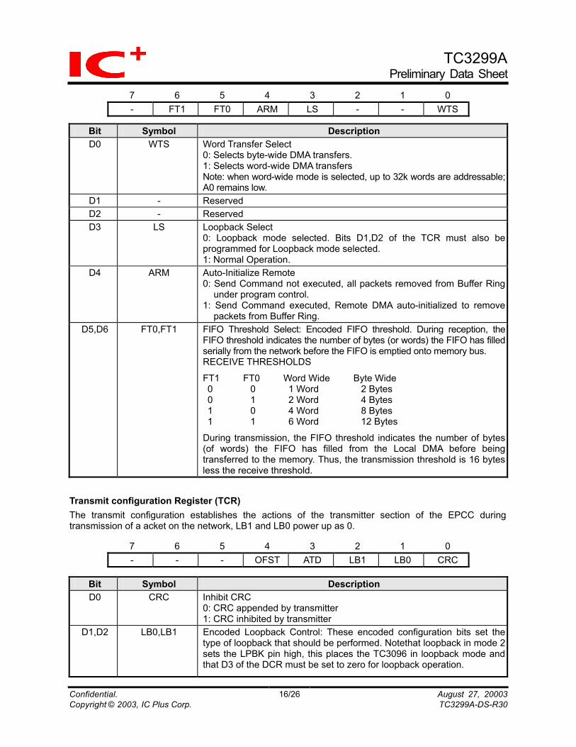
Data Configure register (DCR) This Register is used to program the EPCC for 8 or 16-bit memory interfaces, select byte ordering in 16-bit applications and establish FIFO thresholds. The DCR must be initialized prior to load the Remote Byte count Registers.
Confidential. 15/26 August 27, 20003Copyright © 2003, IC Plus Corp. TC3299A-DS-R30
TC3299APreliminary Data Sheet
7 6 5 4 3 2 1 0 - FT1 FT0 ARM LS - - WTS
Bit Symbol Description D0 WTS Word Transfer Select
0: Selects byte-wide DMA transfers. 1: Selects word-wide DMA transfers Note: when word-wide mode is selected, up to 32k words are addressable; A0 remains low.
D1 - Reserved D2 - Reserved D3 LS Loopback Select
0: Loopback mode selected. Bits D1,D2 of the TCR must also be programmed for Loopback mode selected. 1: Normal Operation.
D4 ARM Auto-Initialize Remote 0: Send Command not executed, all packets removed from Buffer Ring
under program control. 1: Send Command executed, Remote DMA auto-initialized to remove
packets from Buffer Ring. D5,D6 FT0,FT1 FIFO Threshold Select: Encoded FIFO threshold. During reception, the
FIFO threshold indicates the number of bytes (or words) the FIFO has filled serially from the network before the FIFO is emptied onto memory bus. RECEIVE THRESHOLDS
FT1 FT0 Word Wide Byte Wide 0 0 1 Word 2 Bytes 0 1 2 Word 4 Bytes 1 0 4 Word 8 Bytes 1 1 6 Word 12 Bytes
During transmission, the FIFO threshold indicates the number of bytes (of words) the FIFO has filled from the Local DMA before being transferred to the memory. Thus, the transmission threshold is 16 bytes less the receive threshold.
Transmit configuration Register (TCR) The transmit configuration establishes the actions of the transmitter section of the EPCC during transmission of a acket on the network, LB1 and LB0 power up as 0.
7 6 5 4 3 2 1 0 - - - OFST ATD LB1 LB0 CRC
Bit Symbol Description D0 CRC Inhibit CRC
0: CRC appended by transmitter 1: CRC inhibited by transmitter
D1,D2 LB0,LB1 Encoded Loopback Control: These encoded configuration bits set the type of loopback that should be performed. Notethat loopback in mode 2 sets the LPBK pin high, this places the TC3096 in loopback mode and that D3 of the DCR must be set to zero for loopback operation.
Confidential. 16/26 August 27, 20003Copyright © 2003, IC Plus Corp. TC3299A-DS-R30
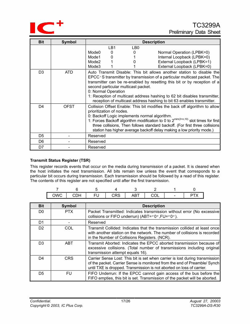
TC3299APreliminary Data Sheet
Bit Symbol Description LB1 LB0 Mode0 0 0 Normal Operation (LPBK=0) Mode1 0 1 Internal Loopback (LPBK=0) Mode2 1 0 External Loopback (LPBK=1) Mode3 1 1 External Loopback (LPBK=0)
D3 ATD Auto Transmit Disable: This bit allows another station to disable the EPCC'S transmitter by transmission of a particular multicast packet. The transmitter can be re-enabled by resetting this bit or by reception of a second particular multicast packet. 0: Normal Operation 1: Reception of multicast address hashing to 62 bit disables transmitter,
reception of multicast address hashing to bit 63 enables transmitter. D4 OFST Collision Offset Enable: This bit modifies the back off algorithm to allow
prioritization of nodes. 0: Backoff Logic implements normal algorithm. 1: Forces Backoff algorithm modification to 0 to 2mim(3+n,10) slot times for first
three collisions, Then follows standard backoff. (For first three collisionsstation has higher average backoff delay making a low priority mode.)
D5 - Reserved D6 - Reserved D7 - Reserved
Transmit Status Register (TSR) This register records events that occur on the media during transmission of a packet. It is cleared when the host initiates the next transmission. All bits remain low unless the event that corresponds to a particular bit occurs during transmission. Each transmission should be followed by a read of this register. The contents of this register are not specified until after the first transmission.
7 6 5 4 3 2 1 0 OWC CDH FU CRS ABT COL - PTX
Bit Symbol Description D0 PTX Packet Transmitted: Indicates transmission without error (No excessive
collisions or FIFO underrun) (ABT=”0”,FU=”0”). D1 - Reserved D2 COL Transmit Collided: Indicates that the transmission collided at least once
with another station on the network. The number of collisions is recorded in the Number of Collisions Registers. (NCR).
D3 ABT Transmit Aborted: Indicates the EPCC aborted transmission because of excessive collisions. (Total number of transmissions including original transmission attempt equals 16).
D4 CRS Carrier Sense Lost: This bit is set when carrier is lost during transmission of the packet. Carrier Sense is monitored from the end of Preamble/ Synch until TXE is dropped. Transmission is not aborted on loss of carrier.
D5 FU FIFO Underrun: If the EPCC cannot gain access of the bus before the FIFO empties, this bit is set. Transmission of the packet will be aborted.
Confidential. 17/26 August 27, 20003Copyright © 2003, IC Plus Corp. TC3299A-DS-R30
TC3299APreliminary Data Sheet
D6 CDH CD Heartbeat: Failure of the transceiver to transmit a collision signal after transmission of a packet will set this bit. The Collision Detect (CD) heartbeat signal must commence during the first 6.4us of the Interframe Gap following a transmission. In certain collisions, the CD Heartbeat bit will be set even though the transceiver is not performing the CD heartbeat test.
D7 OWC Out of Window Collision: Indicates that a collision occurred after a slot time (51.2us). Transmissions rescheduled as in normal collisions.
Receive Configuration Register (RCR) This register determines operation of the EPCC during reception of a packet and is used to program what types of packets to accept.
7 6 5 4 3 2 1 0 - - MON PRO AM AB AR SEP
Bit Symbol Description D0 SEP Save Errored Packets
0: Packets with receive errors are rejected. 1: Packets with receive errors are accepted. Receive errors are CRC and Frame Alignment errors.
D1 AR Accept Runt Packets 0: Packets with fewer than 64 bytes rejected. 1: Packets with fewer than 64 bytes accepted.
D2 AB Accept Broadcast 0: Packets with all 1's broadcast destination address rejected. 1: Packets with all 1's broadcast destination address accepted.
D3 AM Accept Multicast 0: Packets with multicast destination address not checked. 1: Packets with multicast destination address checked.
D4 PRO Promiscuous Physical 0: Physical address of node must match the station address programmed in PAR0-PAR5. (Physical address checked) 1: All packets with any physical address accepted. (physical address not checked)
D5 MON Monitor Mode: Enables the receiver to check addresses and CRC on incoming packets without buffering to memory. The missed packet Tally counter will be incremented for each recognized packet. 0: Packets buffered to memory. 1: Packets checked for address match, good CRC and frame Alignment but not buffered to memory.
D6 - Reserved D7 - Reserved
Note: D2 and D3 are ”OR'd” together, i.e., if D2 and D3 are set the EPCC will accept broadcast and multicast addresses as well as its own physical address. To establish full promiscuous (non discrimination) mode, bits D2, D3 and D4 should be set. In addition the multicast hashing array must be set to all 1's in order to accept all multicast addresses.
Receive Status Register (RSR)
Confidential. 18/26 August 27, 20003Copyright © 2003, IC Plus Corp. TC3299A-DS-R30
TC3299APreliminary Data Sheet
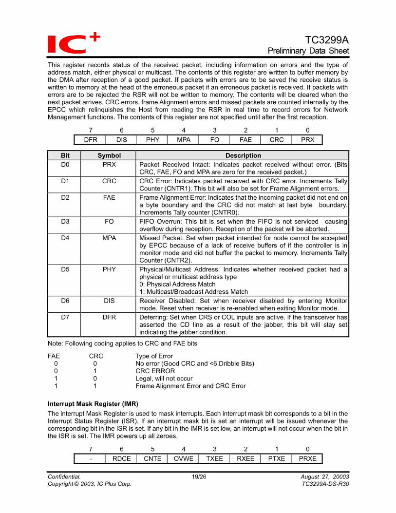
This register records status of the received packet, including information on errors and the type of address match, either physical or multicast. The contents of this register are written to buffer memory by the DMA after reception of a good packet. If packets with errors are to be saved the receive status is written to memory at the head of the erroneous packet if an erroneous packet is received. If packets with errors are to be rejected the RSR will not be written to memory. The contents will be cleared when the next packet arrives. CRC errors, frame Alignment errors and missed packets are counted internally by the EPCC which relinquishes the Host from reading the RSR in real time to record errors for Network Management functions. The contents of this register are not specified until after the first reception.
7 6 5 4 3 2 1 0 DFR DIS PHY MPA FO FAE CRC PRX
Bit Symbol Description D0 PRX Packet Received Intact: Indicates packet received without error. (Bits
CRC, FAE, FO and MPA are zero for the received packet.) D1 CRC CRC Error: Indicates packet received with CRC error. Increments Tally
Counter (CNTR1). This bit will also be set for Frame Alignment errors. D2 FAE Frame Alignment Error: Indicates that the incoming packet did not end on
a byte boundary and the CRC did not match at last byte boundary. Increments Tally counter (CNTR0).
D3 FO FIFO Overrun: This bit is set when the FIFO is not serviced causing overflow during reception. Reception of the packet will be aborted.
D4 MPA Missed Packet: Set when packet intended for node cannot be accepted by EPCC because of a lack of receive buffers of if the controller is in monitor mode and did not buffer the packet to memory. Increments Tally Counter (CNTR2).
D5 PHY Physical/Multicast Address: Indicates whether received packet had a physical or multicast address type 0: Physical Address Match 1: Multicast/Broadcast Address Match
D6 DIS Receiver Disabled: Set when receiver disabled by entering Monitor mode. Reset when receiver is re-enabled when exiting Monitor mode.
D7 DFR Deferring: Set when CRS or COL inputs are active. If the transceiver has asserted the CD line as a result of the jabber, this bit will stay set indicating the jabber condition.
Note: Following coding applies to CRC and FAE bits FAE CRC Type of Error 0 0 No error (Good CRC and <6 Dribble Bits) 0 1 CRC ERROR 1 0 Legal, will not occur 1 1 Frame Alignment Error and CRC Error Interrupt Mask Register (IMR) The interrupt Mask Register is used to mask interrupts. Each interrupt mask bit corresponds to a bit in the Interrupt Status Register (ISR). If an interrupt mask bit is set an interrupt will be issued whenever the corresponding bit in the ISR is set. If any bit in the IMR is set low, an interrupt will not occur when the bit in the ISR is set. The IMR powers up all zeroes.
7 6 5 4 3 2 1 0 - RDCE CNTE OVWE TXEE RXEE PTXE PRXE
Confidential. 19/26 August 27, 20003Copyright © 2003, IC Plus Corp. TC3299A-DS-R30

TC3299APreliminary Data Sheet
Bit Symbol Description D0 PRXE Packet Received Interrupt Enable: Enables Interrupt when packet received.D1 PTXE Packet Transmitted Interrupt Enable: Enables Interrupt when packet is
transmitted. D2 RXEE Receive Error Interrupt Enable: Enables Interrupt when packet received
with error. D3 TXEE Transmit Error Interrupt Enable: Enables Interrupt when packet
transmission results in error. D4 OVWE Over Write Warning Interrupt Enable: Enables Interrupt when Buffer
management Logic lacks sufficient buffers to store incoming packet. D5 CNTE Counter Overflow Interrupt Enable: Enables Interrupt when MSB of one
or more of the Network Tally counters has been set. D6 RDCE DMA Complete Interrupt Enable: Enables Interrupt when Remote DMA
transfer has been completed. D7 - Reserved
Interrupt Status Register (ISR) This register is accessed to determine the cause of an interrupt. Any interrupt can be masked in the interrupt Mask Register (IMR). Individual interrupt bit is cleared by writing a ”1” into the corresponding bit of the ISR. The IRQ signal is active as long as any unmasked signal is set, and will not go low until all unmarked bits in this register have been cleared. The ISR must be cleared after power up by writing it with all 1's.
7 6 5 4 3 2 1 0 RST RDC CNT OVW TXE RXE PTX PRX
Bit Symbol Description D0 PRX Packet Received: Indicates packet received with no errors. D1 PTX Packet Transmitted: Indicates packet transmitted with no errors. D2 RXE Receive Error: Indicates that a packet was received with one or more of
the following errors: - CRC Error - Frame Alignment Error - FIFO Overrun - Missed Packet
D3 TXE Transmit Error: Set when packet transmitted with one or more of the following errors: - Excessive Collisions - FIFO Underrun
D4 OVW Over Write Warning: Set when receive buffer ring storage resources have been exhausted. (Local DMA has reached Boundary Pointer).
D5 CNT Counter Over flow: Set when MSB of one or more of the Network Tally Counters has been set.
D6 RDC Remote DMA Complete: Set when Remote DMA operation has been completed.
D7 RST Reset Status: A status indicator with no interrupt generated - Set when EPCC enters reset state and is cleared when a start
command is issued - Set when a Receive Buffer Ring overflows and is cleared when leaves
overflow status. Writing to this bit has no effect and powers up high.
Confidential. 20/26 August 27, 20003Copyright © 2003, IC Plus Corp. TC3299A-DS-R30
TC3299APreliminary Data Sheet
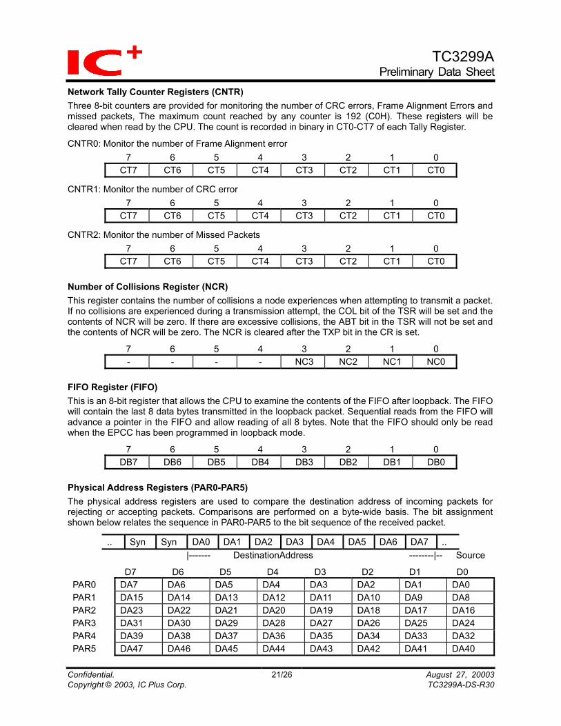
Network Tally Counter Registers (CNTR) Three 8-bit counters are provided for monitoring the number of CRC errors, Frame Alignment Errors and missed packets, The maximum count reached by any counter is 192 (C0H). These registers will be cleared when read by the CPU. The count is recorded in binary in CT0-CT7 of each Tally Register.
CNTR0: Monitor the number of Frame Alignment error 7 6 5 4 3 2 1 0
CT7 CT6 CT5 CT4 CT3 CT2 CT1 CT0
CNTR1: Monitor the number of CRC error 7 6 5 4 3 2 1 0
CT7 CT6 CT5 CT4 CT3 CT2 CT1 CT0
CNTR2: Monitor the number of Missed Packets 7 6 5 4 3 2 1 0
CT7 CT6 CT5 CT4 CT3 CT2 CT1 CT0
Number of Collisions Register (NCR) This register contains the number of collisions a node experiences when attempting to transmit a packet. If no collisions are experienced during a transmission attempt, the COL bit of the TSR will be set and the contents of NCR will be zero. If there are excessive collisions, the ABT bit in the TSR will not be set and the contents of NCR will be zero. The NCR is cleared after the TXP bit in the CR is set.
7 6 5 4 3 2 1 0 - - - - NC3 NC2 NC1 NC0
FIFO Register (FIFO) This is an 8-bit register that allows the CPU to examine the contents of the FIFO after loopback. The FIFO will contain the last 8 data bytes transmitted in the loopback packet. Sequential reads from the FIFO will advance a pointer in the FIFO and allow reading of all 8 bytes. Note that the FIFO should only be read when the EPCC has been programmed in loopback mode.
7 6 5 4 3 2 1 0 DB7 DB6 DB5 DB4 DB3 DB2 DB1 DB0
Physical Address Registers (PAR0-PAR5) The physical address registers are used to compare the destination address of incoming packets for rejecting or accepting packets. Comparisons are performed on a byte-wide basis. The bit assignment shown below relates the sequence in PAR0-PAR5 to the bit sequence of the received packet.
.. Syn Syn DA0 DA1 DA2 DA3 DA4 DA5 DA6 DA7 .. |------- DestinationAddress --------|-- Source
D7 D6 D5 D4 D3 D2 D1 D0 PAR0 DA7 DA6 DA5 DA4 DA3 DA2 DA1 DA0 PAR1 DA15 DA14 DA13 DA12 DA11 DA10 DA9 DA8 PAR2 DA23 DA22 DA21 DA20 DA19 DA18 DA17 DA16 PAR3 DA31 DA30 DA29 DA28 DA27 DA26 DA25 DA24 PAR4 DA39 DA38 DA37 DA36 DA35 DA34 DA33 DA32 PAR5 DA47 DA46 DA45 DA44 DA43 DA42 DA41 DA40
Confidential. 21/26 August 27, 20003Copyright © 2003, IC Plus Corp. TC3299A-DS-R30
TC3299APreliminary Data Sheet
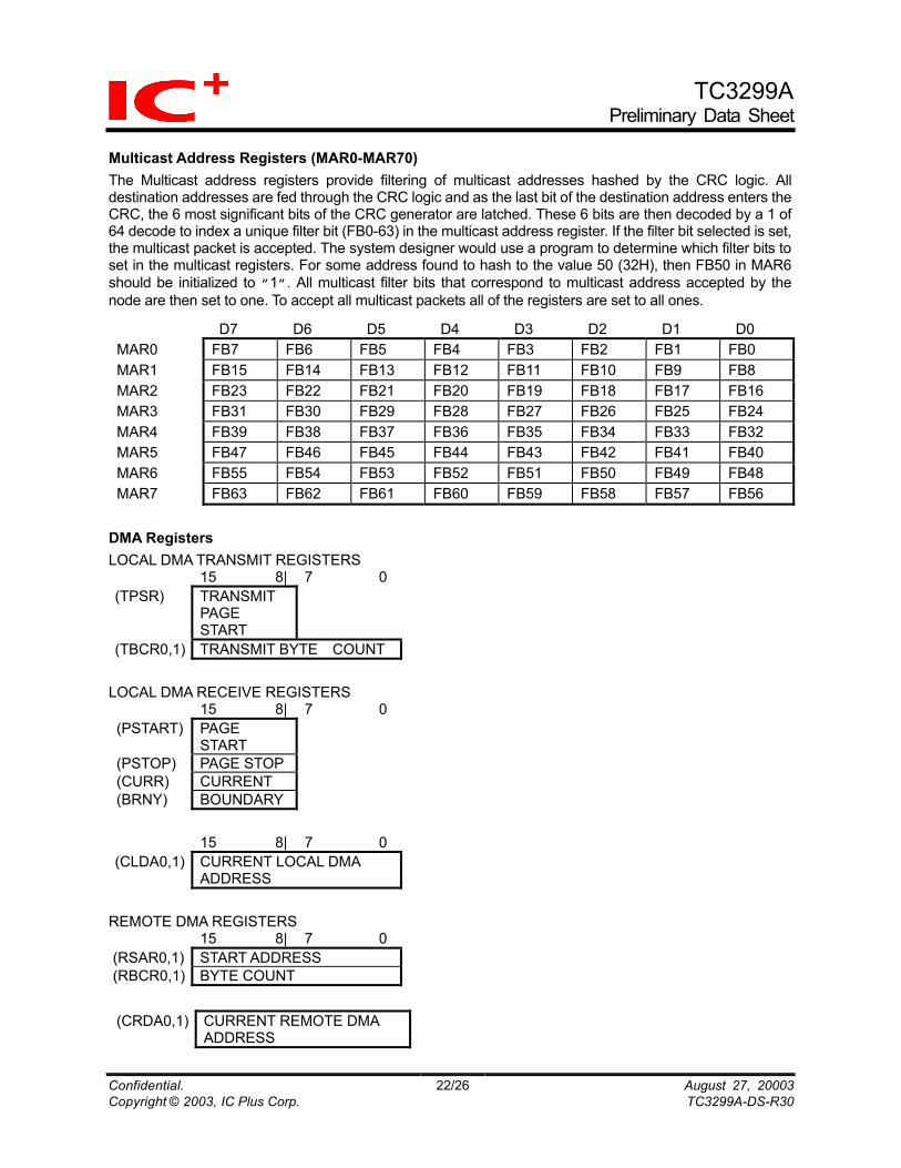
Multicast Address Registers (MAR0-MAR70) The Multicast address registers provide filtering of multicast addresses hashed by the CRC logic. All destination addresses are fed through the CRC logic and as the last bit of the destination address enters the CRC, the 6 most significant bits of the CRC generator are latched. These 6 bits are then decoded by a 1 of 64 decode to index a unique filter bit (FB0-63) in the multicast address register. If the filter bit selected is set, the multicast packet is accepted. The system designer would use a program to determine which filter bits to set in the multicast registers. For some address found to hash to the value 50 (32H), then FB50 in MAR6 should be initialized to ”1”. All multicast filter bits that correspond to multicast address accepted by the node are then set to one. To accept all multicast packets all of the registers are set to all ones. D7 D6 D5 D4 D3 D2 D1 D0 MAR0 FB7 FB6 FB5 FB4 FB3 FB2 FB1 FB0 MAR1 FB15 FB14 FB13 FB12 FB11 FB10 FB9 FB8 MAR2 FB23 FB22 FB21 FB20 FB19 FB18 FB17 FB16 MAR3 FB31 FB30 FB29 FB28 FB27 FB26 FB25 FB24 MAR4 FB39 FB38 FB37 FB36 FB35 FB34 FB33 FB32 MAR5 FB47 FB46 FB45 FB44 FB43 FB42 FB41 FB40 MAR6 FB55 FB54 FB53 FB52 FB51 FB50 FB49 FB48 MAR7 FB63 FB62 FB61 FB60 FB59 FB58 FB57 FB56
DMA Registers LOCAL DMA TRANSMIT REGISTERS 15 8| 7 0 (TPSR) TRANSMIT
PAGE START
(TBCR0,1) TRANSMIT BYTE COUNT LOCAL DMA RECEIVE REGISTERS 15 8| 7 0 (PSTART) PAGE
START
(PSTOP) PAGE STOP (CURR) CURRENT (BRNY) BOUNDARY
15 8| 7 0 (CLDA0,1) CURRENT LOCAL DMA
ADDRESS REMOTE DMA REGISTERS 15 8| 7 0 (RSAR0,1) START ADDRESS (RBCR0,1) BYTE COUNT
(CRDA0,1) CURRENT REMOTE DMA ADDRESS
Confidential. 22/26 August 27, 20003Copyright © 2003, IC Plus Corp. TC3299A-DS-R30
TC3299APreliminary Data Sheet
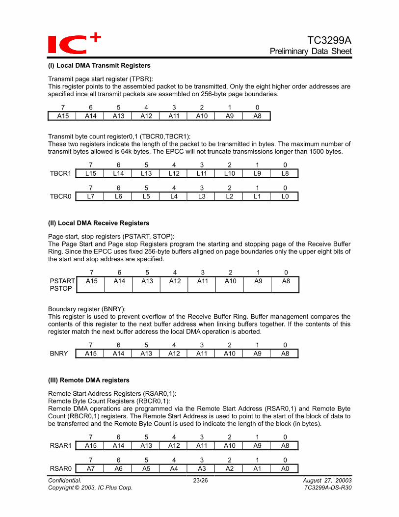
(I) Local DMA Transmit Registers Transmit page start register (TPSR): This register points to the assembled packet to be transmitted. Only the eight higher order addresses are specified ince all transmit packets are assembled on 256-byte page boundaries.
7 6 5 4 3 2 1 0 A15 A14 A13 A12 A11 A10 A9 A8
Transmit byte count register0,1 (TBCR0,TBCR1): These two registers indicate the length of the packet to be transmitted in bytes. The maximum number of transmit bytes allowed is 64k bytes. The EPCC will not truncate transmissions longer than 1500 bytes. 7 6 5 4 3 2 1 0 TBCR1 L15 L14 L13 L12 L11 L10 L9 L8
7 6 5 4 3 2 1 0 TBCR0 L7 L6 L5 L4 L3 L2 L1 L0
(II) Local DMA Receive Registers Page start, stop registers (PSTART, STOP): The Page Start and Page stop Registers program the starting and stopping page of the Receive Buffer Ring. Since the EPCC uses fixed 256-byte buffers aligned on page boundaries only the upper eight bits of the start and stop address are specified. 7 6 5 4 3 2 1 0 PSTART PSTOP
A15 A14 A13 A12 A11 A10 A9 A8
Boundary register (BNRY): This register is used to prevent overflow of the Receive Buffer Ring. Buffer management compares the contents of this register to the next buffer address when linking buffers together. If the contents of this register match the next buffer address the local DMA operation is aborted. 7 6 5 4 3 2 1 0 BNRY A15 A14 A13 A12 A11 A10 A9 A8
(III) Remote DMA registers Remote Start Address Registers (RSAR0,1): Remote Byte Count Registers (RBCR0,1): Remote DMA operations are programmed via the Remote Start Address (RSAR0,1) and Remote Byte Count (RBCR0,1) registers. The Remote Start Address is used to point to the start of the block of data to be transferred and the Remote Byte Count is used to indicate the length of the block (in bytes). 7 6 5 4 3 2 1 0 RSAR1 A15 A14 A13 A12 A11 A10 A9 A8
7 6 5 4 3 2 1 0 RSAR0 A7 A6 A5 A4 A3 A2 A1 A0
Confidential. 23/26 August 27, 20003Copyright © 2003, IC Plus Corp. TC3299A-DS-R30
TC3299APreliminary Data Sheet
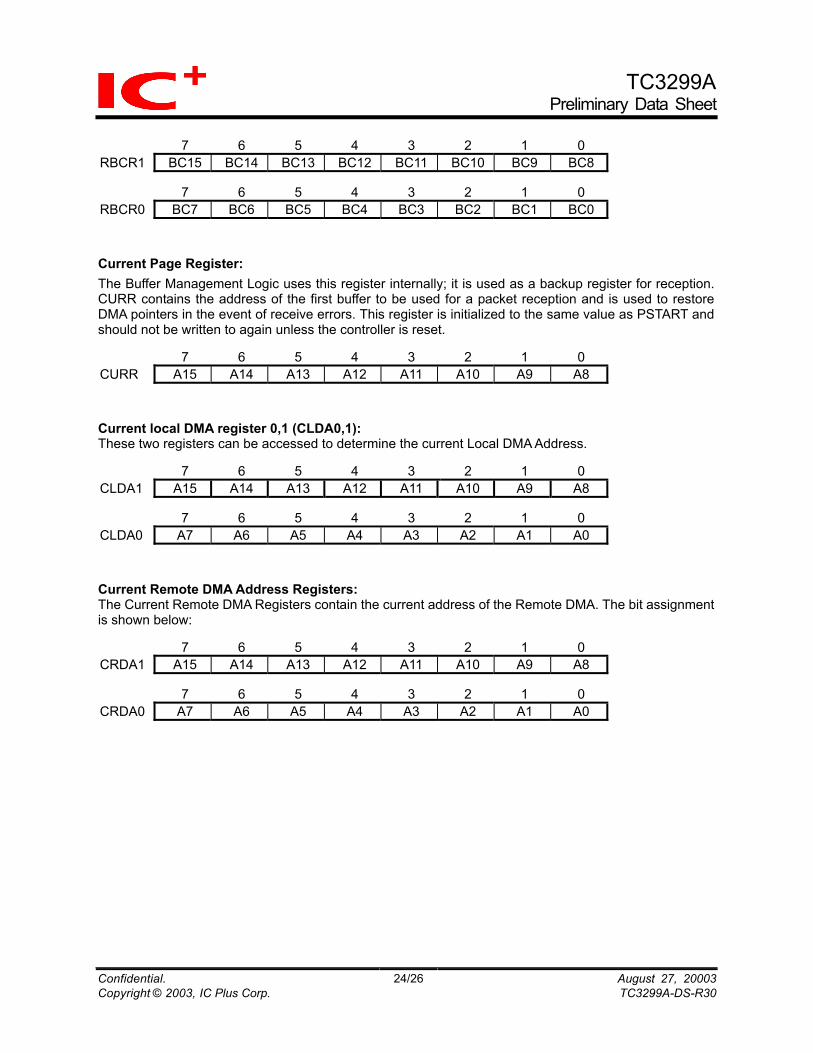
7 6 5 4 3 2 1 0 RBCR1 BC15 BC14 BC13 BC12 BC11 BC10 BC9 BC8 7 6 5 4 3 2 1 0 RBCR0 BC7 BC6 BC5 BC4 BC3 BC2 BC1 BC0 Current Page Register: The Buffer Management Logic uses this register internally; it is used as a backup register for reception. CURR contains the address of the first buffer to be used for a packet reception and is used to restore DMA pointers in the event of receive errors. This register is initialized to the same value as PSTART and should not be written to again unless the controller is reset. 7 6 5 4 3 2 1 0 CURR A15 A14 A13 A12 A11 A10 A9 A8 Current local DMA register 0,1 (CLDA0,1): These two registers can be accessed to determine the current Local DMA Address. 7 6 5 4 3 2 1 0 CLDA1 A15 A14 A13 A12 A11 A10 A9 A8 7 6 5 4 3 2 1 0 CLDA0 A7 A6 A5 A4 A3 A2 A1 A0 Current Remote DMA Address Registers: The Current Remote DMA Registers contain the current address of the Remote DMA. The bit assignment is shown below: 7 6 5 4 3 2 1 0 CRDA1 A15 A14 A13 A12 A11 A10 A9 A8 7 6 5 4 3 2 1 0 CRDA0 A7 A6 A5 A4 A3 A2 A1 A0
Confidential. 24/26 August 27, 20003Copyright © 2003, IC Plus Corp. TC3299A-DS-R30
TC3299APreliminary Data Sheet
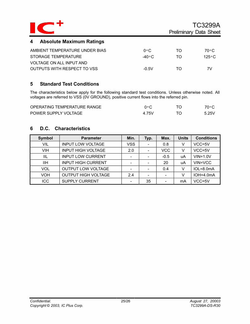
4 Absolute Maximum Ratings AMBIENT TEMPERATURE UNDER BIAS 0°C TO 70°C STORAGE TEMPERATURE -40°C TO 125°C VOLTAGE ON ALL INPUT AND OUTPUTS WITH RESPECT TO VSS -0.5V TO 7V 5 Standard Test Conditions The characteristics below apply for the following standard test conditions. Unless otherwise noted. All voltages are referred to VSS (0V GROUND), positive current flows into the referred pin. OPERATING TEMPERATURE RANGE 0°C TO 70°C POWER SUPPLY VOLTAGE 4.75V TO 5.25V 6 D.C. Characteristics
Symbol Parameter Min. Typ. Max. Units ConditionsVIL INPUT LOW VOLTAGE VSS - 0.8 V VCC=5V VIH INPUT HIGH VOLTAGE 2.0 - VCC V VCC=5V IIL INPUT LOW CURRENT - - -0.5 uA VIN=1.0V IIH INPUT HIGH CURRENT - - 20 uA VIN=VCC
VOL OUTPUT LOW VOLTAGE - - 0.4 V IOL=8.0mA VOH OUTPUT HIGH VOLTAGE 2.4 - - V IOH=4.0mA ICC SUPPLY CURRENT - 35 - mA VCC=5V
Confidential. 25/26 August 27, 20003Copyright © 2003, IC Plus Corp. TC3299A-DS-R30
TC3299APreliminary Data Sheet
Confidential. 26/26 August 27, 20003Copyright © 2003, IC Plus Corp. TC3299A-DS-R30
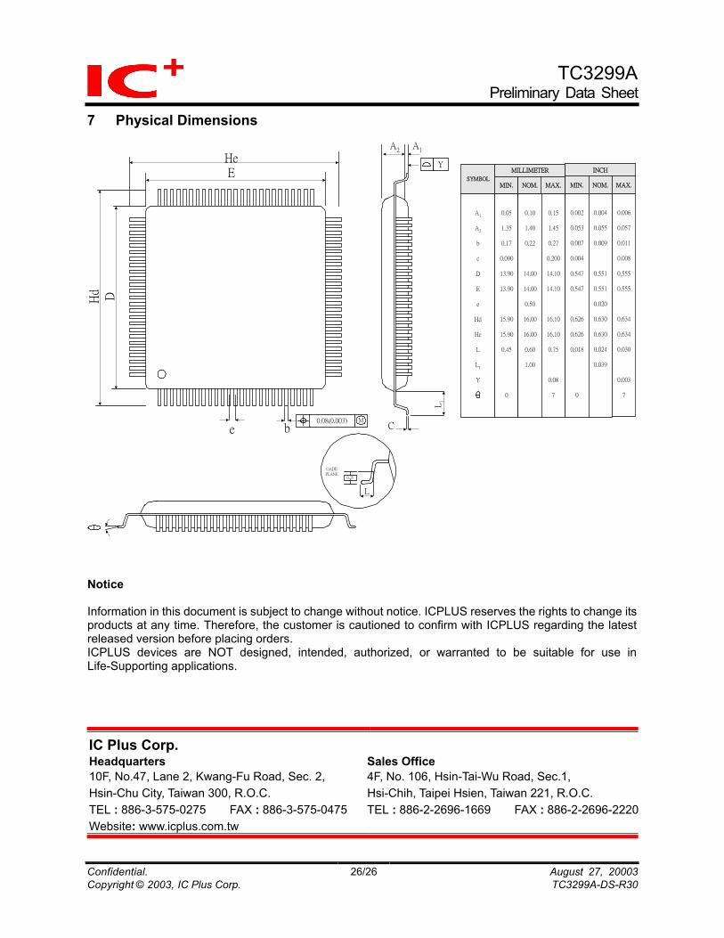
7 Physical Dimensions DHd
EHe
b0.08(0.003) M
e CL1
A2
A1
Y
0.25
GADEPLANE
L
A1
A2
b
c
D
E
e
Hd
He
L
L1
Y
SYMBOL
MILLIMETER
MIN. NOM. MAX.
0.05
1.35
0.17
0.090
13.90
13.90
15.90
15.90
0.45
0
0.10
1.40
0.22
14.00
14.00
0.50
16.00
16.00
0.60
1.00
0.15
1.45
0.27
0.200
14.10
14.10
16.10
16.10
0.75
0.08
7
INCH
MIN. NOM. MAX.
0.002
0.053
0.007
0.004
0.547
0.547
0.626
0.626
0.018
0
0.004
0.055
0.009
0.551
0.551
0.020
0.630
0.630
0.024
0.039
0.006
0.057
0.011
0.008
0.555
0.555
0.634
0.634
0.030
0.003
7
Notice Information in this document is subject to change without notice. ICPLUS reserves the rights to change its products at any time. Therefore, the customer is cautioned to confirm with ICPLUS regarding the latest released version before placing orders. ICPLUS devices are NOT designed, intended, authorized, or warranted to be suitable for use in Life-Supporting applications.
IC Plus Corp. Headquarters Sales Office 10F, No.47, Lane 2, Kwang-Fu Road, Sec. 2, 4F, No. 106, Hsin-Tai-Wu Road, Sec.1, Hsin-Chu City, Taiwan 300, R.O.C. Hsi-Chih, Taipei Hsien, Taiwan 221, R.O.C. TEL : 886-3-575-0275 FAX : 886-3-575-0475 TEL : 886-2-2696-1669 FAX : 886-2-2696-2220Website: www.icplus.com.tw


![Certificate in Laptop Repairing - maharishiskills.commaharishiskills.com/wp-content/uploads/2019/03/... · • INTEGRATED CIRCUITS [IC] PCMCIA CARD &DVD DRIVE 1. What is pcmcia card?](https://cdn.vdocuments.site/doc/165x107/60845169f37fcd7f1b44f9e3/certificate-in-laptop-repairing-a-integrated-circuits-ic-pcmcia-card-dvd.jpg)