Chapter 9: Sequential Logic Modules
Digital System Designs and Practices Using Verilog HDL and FPGAs @ 2008~2010, John Wiley 9-1
Chapter 9: Sequential Logic Modules
Department of Electronic Engineering
National Taiwan University of Science and Technology
Prof. Ming-Bo Lin
Chapter 9: Sequential Logic Modules
Digital System Designs and Practices Using Verilog HDL and FPGAs @ 2008~2010, John Wiley 9-2
Syllabus
ObjectivesFundamentals of sequential logic modulesFlip-flopsMemory elementsShift registersCountersSequence generatorsTiming generators
Chapter 9: Sequential Logic Modules
Digital System Designs and Practices Using Verilog HDL and FPGAs @ 2008~2010, John Wiley 9-3
ObjectivesAfter completing this chapter, you will be able to:
Describe how to model asynchronous and synchronous D-type flip-flopsDescribe how to model registers (data register, register file, and synchronous RAM)Describe how to model shift registers Describe how to model counters (ripple/synchronous counters and modulo r counters)Describe how to model sequence generatorsDescribe how to model timing generators
Chapter 9: Sequential Logic Modules
Digital System Designs and Practices Using Verilog HDL and FPGAs @ 2008~2010, John Wiley 9-4
Syllabus
ObjectivesFundamentals of sequential logic modulesFlip-flopsMemory elementsShift registersCountersSequence generatorsTiming generators
Chapter 9: Sequential Logic Modules
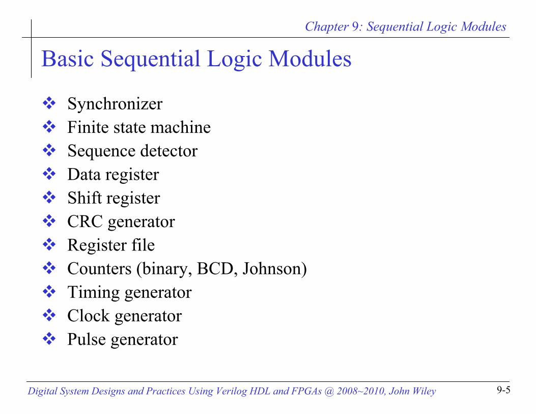
Digital System Designs and Practices Using Verilog HDL and FPGAs @ 2008~2010, John Wiley 9-5
Basic Sequential Logic Modules
Synchronizer Finite state machine Sequence detectorData registerShift register CRC generator Register file Counters (binary, BCD, Johnson)Timing generatorClock generatorPulse generator
Chapter 9: Sequential Logic Modules
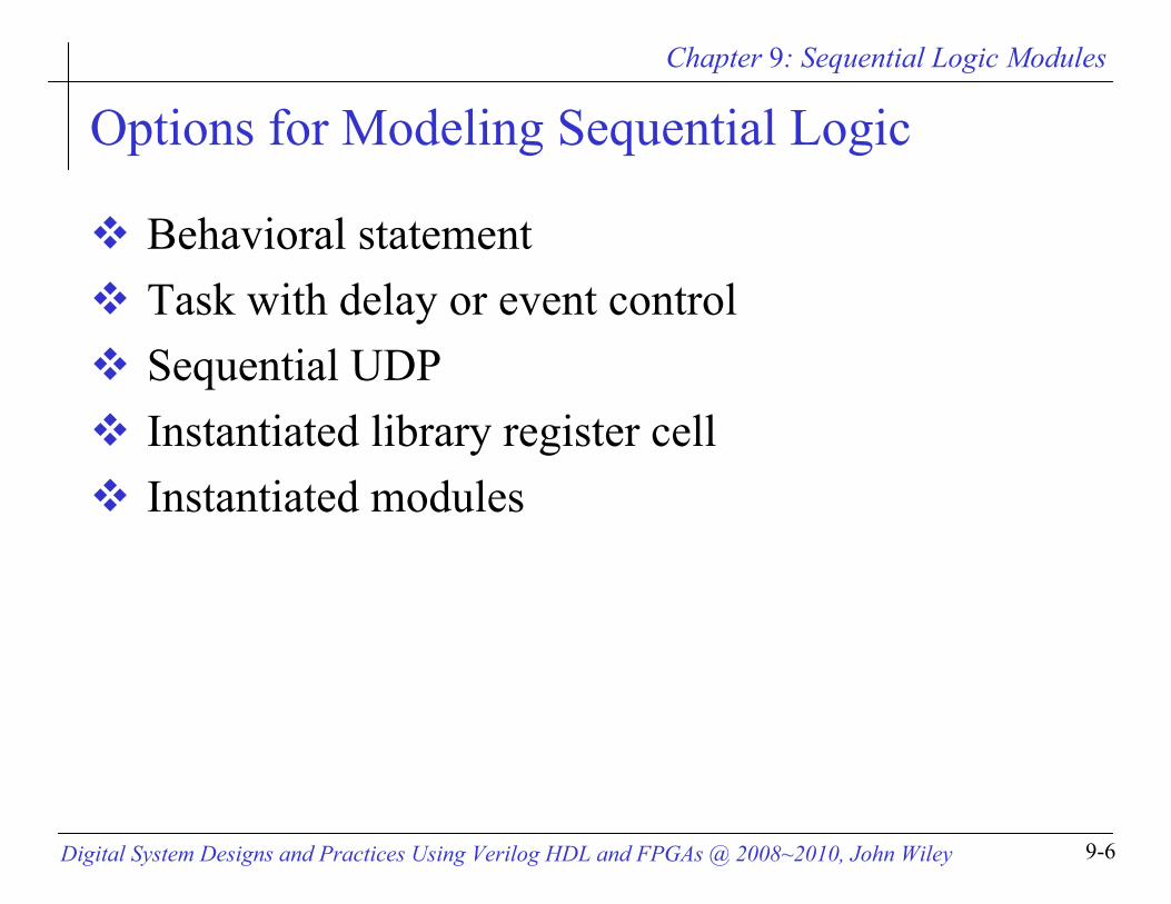
Digital System Designs and Practices Using Verilog HDL and FPGAs @ 2008~2010, John Wiley 9-6
Options for Modeling Sequential Logic
Behavioral statementTask with delay or event controlSequential UDPInstantiated library register cellInstantiated modules
Chapter 9: Sequential Logic Modules
Digital System Designs and Practices Using Verilog HDL and FPGAs @ 2008~2010, John Wiley 9-7
Syllabus
ObjectivesFundamentals of sequential logic modulesFlip-flopsMemory elementsShift registersCountersSequence generatorsTiming generators
Chapter 9: Sequential Logic Modules
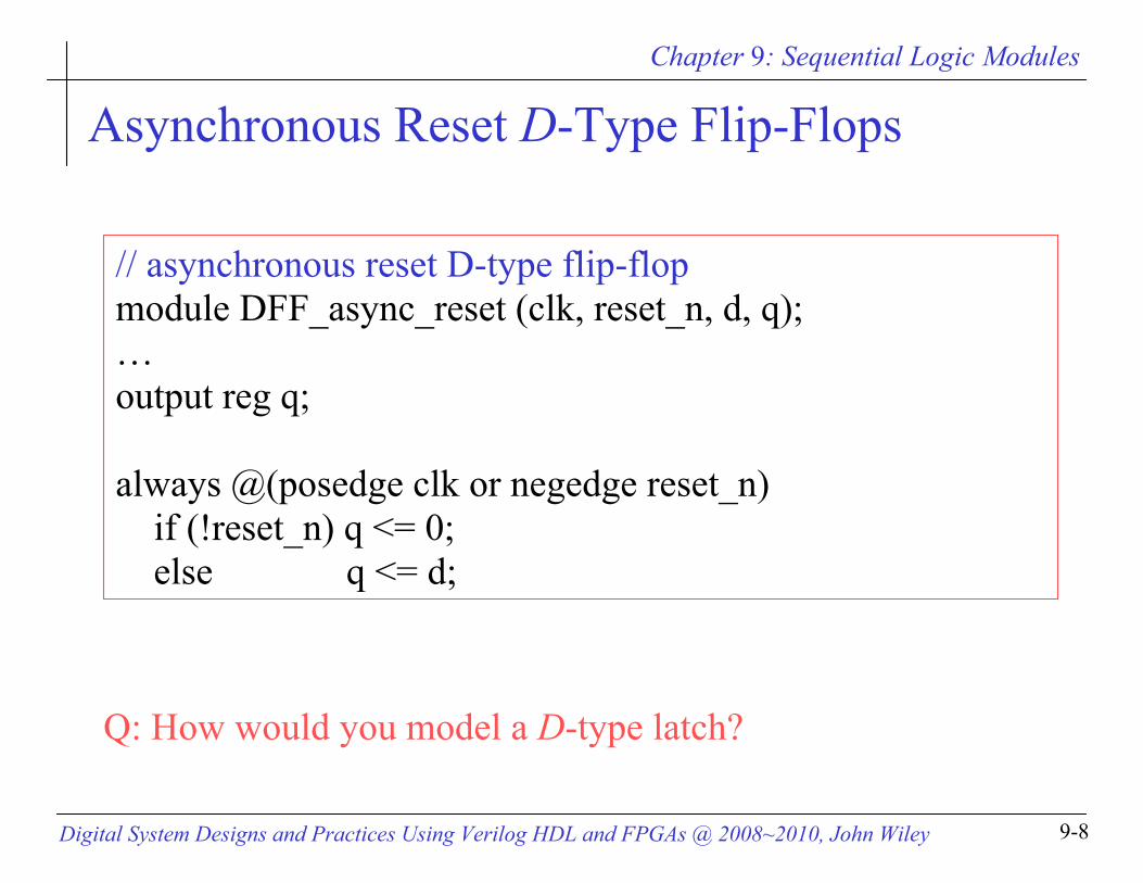
Digital System Designs and Practices Using Verilog HDL and FPGAs @ 2008~2010, John Wiley 9-8
Asynchronous Reset D-Type Flip-Flops
// asynchronous reset D-type flip-flopmodule DFF_async_reset (clk, reset_n, d, q);…output reg q;
always @(posedge clk or negedge reset_n)if (!reset_n) q <= 0; else q <= d;
Q: How would you model a D-type latch?
Chapter 9: Sequential Logic Modules
Digital System Designs and Practices Using Verilog HDL and FPGAs @ 2008~2010, John Wiley 9-9
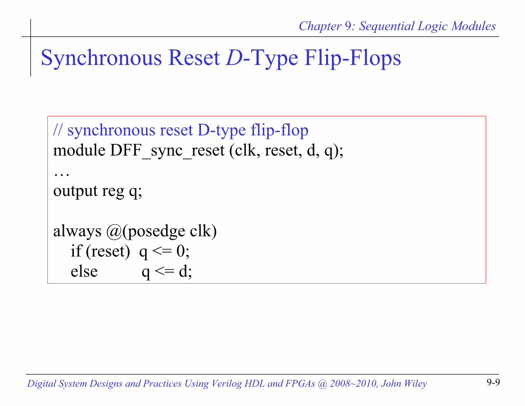
Synchronous Reset D-Type Flip-Flops
// synchronous reset D-type flip-flopmodule DFF_sync_reset (clk, reset, d, q);…output reg q;
always @(posedge clk)if (reset) q <= 0; else q <= d;
Chapter 9: Sequential Logic Modules
Digital System Designs and Practices Using Verilog HDL and FPGAs @ 2008~2010, John Wiley 9-10
Syllabus
ObjectivesFundamentals of sequential logic modulesFlip-flopsMemory elementsShift registersCountersSequence generatorsTiming generators
Chapter 9: Sequential Logic Modules
Digital System Designs and Practices Using Verilog HDL and FPGAs @ 2008~2010, John Wiley 9-11
Types of Memory Elements
Data registersRegister filesSynchronous RAMs
Chapter 9: Sequential Logic Modules
Digital System Designs and Practices Using Verilog HDL and FPGAs @ 2008~2010, John Wiley 9-12
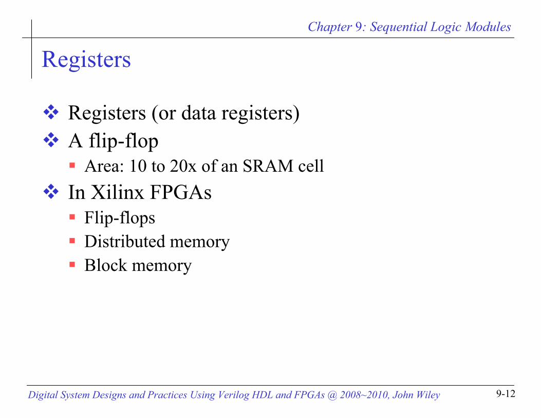
Registers
Registers (or data registers) A flip-flop
Area: 10 to 20x of an SRAM cellIn Xilinx FPGAs
Flip-flopsDistributed memoryBlock memory
Chapter 9: Sequential Logic Modules
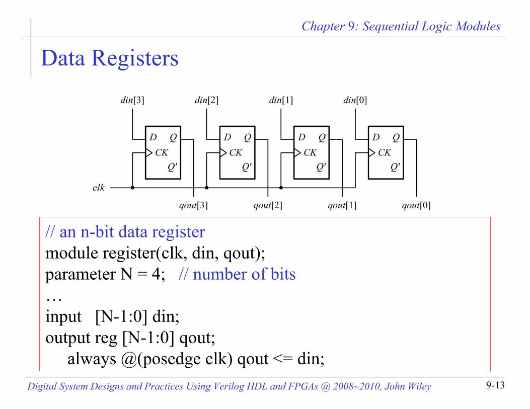
Digital System Designs and Practices Using Verilog HDL and FPGAs @ 2008~2010, John Wiley 9-13
Data Registers
// an n-bit data registermodule register(clk, din, qout);parameter N = 4; // number of bits…input [N-1:0] din;output reg [N-1:0] qout;
always @(posedge clk) qout <= din;
Chapter 9: Sequential Logic Modules
Digital System Designs and Practices Using Verilog HDL and FPGAs @ 2008~2010, John Wiley 9-14
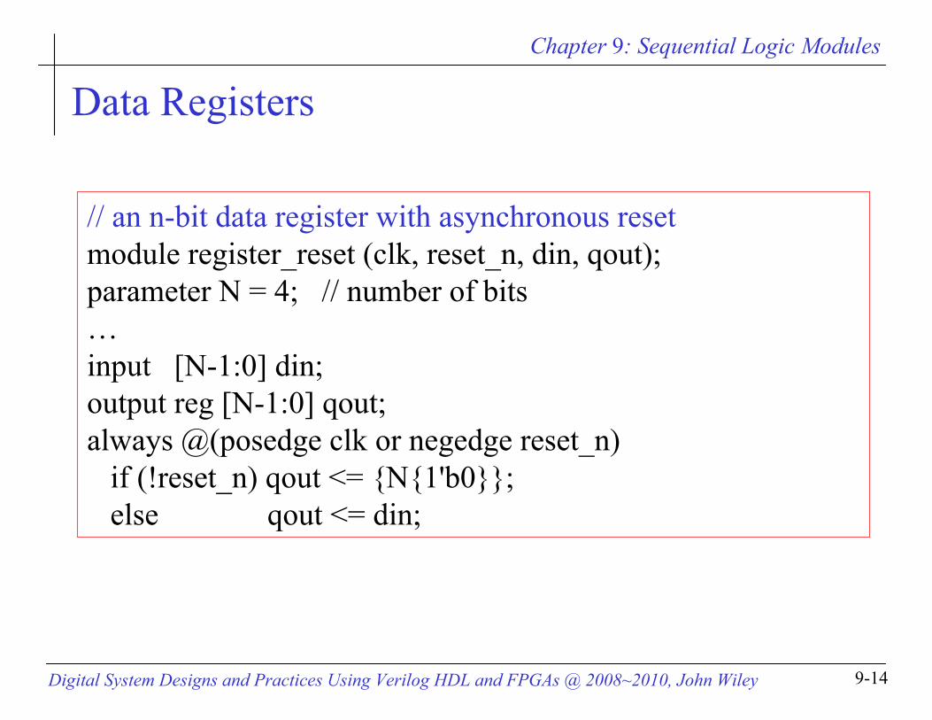
Data Registers
// an n-bit data register with asynchronous resetmodule register_reset (clk, reset_n, din, qout);parameter N = 4; // number of bits…input [N-1:0] din;output reg [N-1:0] qout;always @(posedge clk or negedge reset_n)
if (!reset_n) qout <= {N{1'b0}}; else qout <= din;
Chapter 9: Sequential Logic Modules
Digital System Designs and Practices Using Verilog HDL and FPGAs @ 2008~2010, John Wiley 9-15
Data Registers
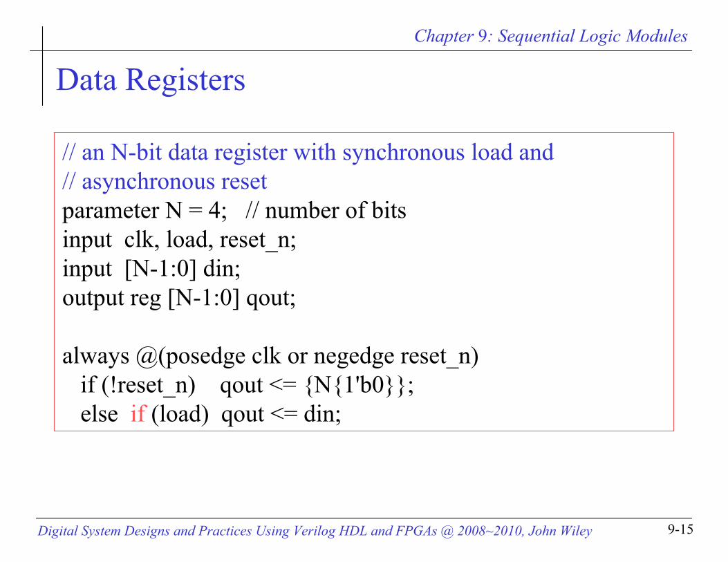
// an N-bit data register with synchronous load and // asynchronous resetparameter N = 4; // number of bitsinput clk, load, reset_n; input [N-1:0] din;output reg [N-1:0] qout;
always @(posedge clk or negedge reset_n)if (!reset_n) qout <= {N{1'b0}}; else if (load) qout <= din;
Chapter 9: Sequential Logic Modules
Digital System Designs and Practices Using Verilog HDL and FPGAs @ 2008~2010, John Wiley 9-16
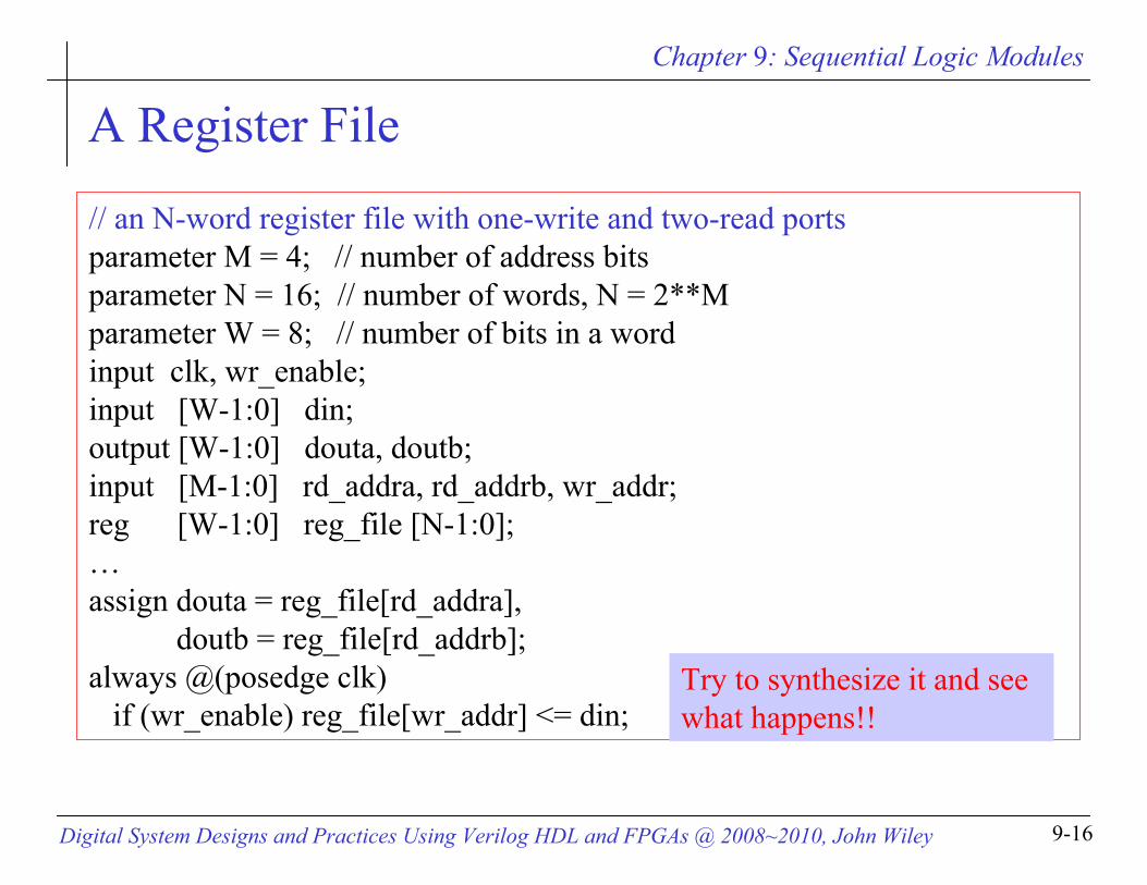
A Register File
// an N-word register file with one-write and two-read portsparameter M = 4; // number of address bitsparameter N = 16; // number of words, N = 2**Mparameter W = 8; // number of bits in a wordinput clk, wr_enable;input [W-1:0] din;output [W-1:0] douta, doutb;input [M-1:0] rd_addra, rd_addrb, wr_addr;reg [W-1:0] reg_file [N-1:0];…assign douta = reg_file[rd_addra],
doutb = reg_file[rd_addrb];always @(posedge clk)
if (wr_enable) reg_file[wr_addr] <= din;Try to synthesize it and see what happens!!
Chapter 9: Sequential Logic Modules
Digital System Designs and Practices Using Verilog HDL and FPGAs @ 2008~2010, John Wiley 9-17
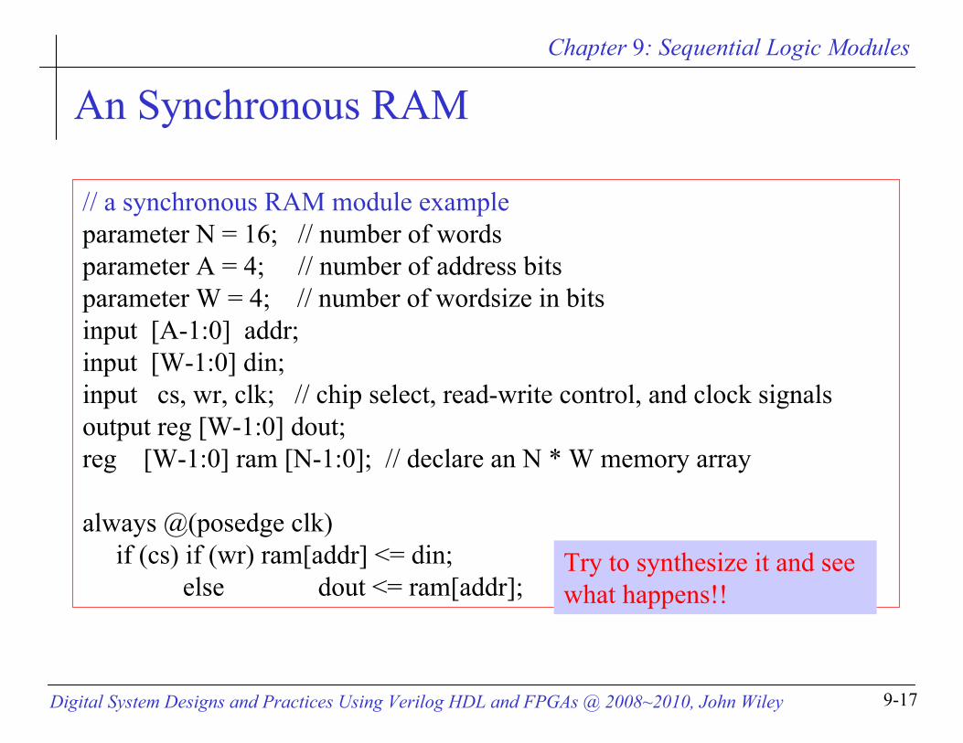
An Synchronous RAM
// a synchronous RAM module exampleparameter N = 16; // number of wordsparameter A = 4; // number of address bitsparameter W = 4; // number of wordsize in bitsinput [A-1:0] addr;input [W-1:0] din;input cs, wr, clk; // chip select, read-write control, and clock signalsoutput reg [W-1:0] dout;reg [W-1:0] ram [N-1:0]; // declare an N * W memory array
always @(posedge clk)if (cs) if (wr) ram[addr] <= din;
else dout <= ram[addr];Try to synthesize it and see what happens!!
Chapter 9: Sequential Logic Modules
Digital System Designs and Practices Using Verilog HDL and FPGAs @ 2008~2010, John Wiley 9-18
Syllabus
ObjectivesFundamentals of sequential logic modulesFlip-flopsMemory elementsShift registersCountersSequence generatorsTiming generators
Chapter 9: Sequential Logic Modules
Digital System Designs and Practices Using Verilog HDL and FPGAs @ 2008~2010, John Wiley 9-19
Shift Registers
Shift registers Parallel/serial format conversion
SISO (serial in serial out)SIPO (serial in parallel out)PISO (parallel in serial out)PIPO (parallel in parallel out)
Chapter 9: Sequential Logic Modules
Digital System Designs and Practices Using Verilog HDL and FPGAs @ 2008~2010, John Wiley 9-20
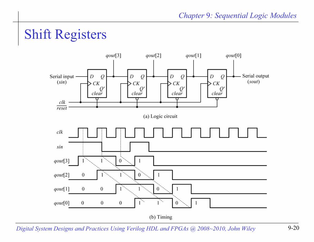
Shift Registers
Chapter 9: Sequential Logic Modules
Digital System Designs and Practices Using Verilog HDL and FPGAs @ 2008~2010, John Wiley 9-21
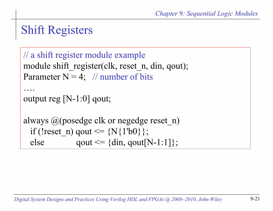
Shift Registers
// a shift register module examplemodule shift_register(clk, reset_n, din, qout);Parameter N = 4; // number of bits….output reg [N-1:0] qout;
always @(posedge clk or negedge reset_n)if (!reset_n) qout <= {N{1'b0}}; else qout <= {din, qout[N-1:1]};
Chapter 9: Sequential Logic Modules
Digital System Designs and Practices Using Verilog HDL and FPGAs @ 2008~2010, John Wiley 9-22
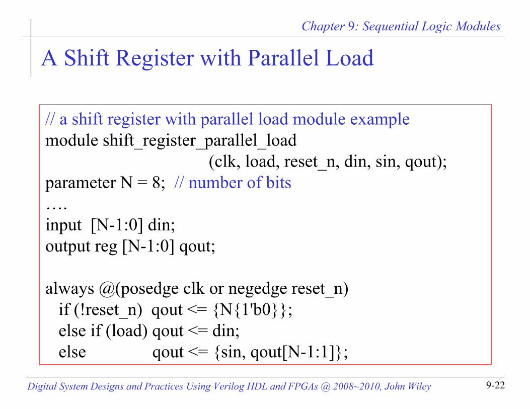
A Shift Register with Parallel Load
// a shift register with parallel load module examplemodule shift_register_parallel_load
(clk, load, reset_n, din, sin, qout);parameter N = 8; // number of bits….input [N-1:0] din; output reg [N-1:0] qout;
always @(posedge clk or negedge reset_n)if (!reset_n) qout <= {N{1'b0}}; else if (load) qout <= din;else qout <= {sin, qout[N-1:1]};
Chapter 9: Sequential Logic Modules
Digital System Designs and Practices Using Verilog HDL and FPGAs @ 2008~2010, John Wiley 9-23
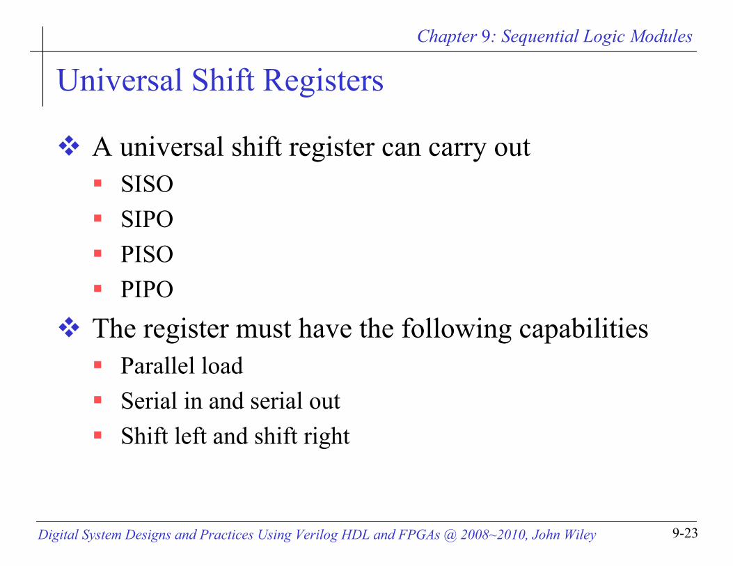
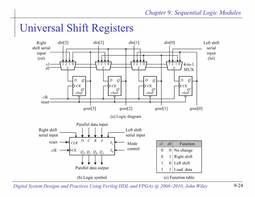
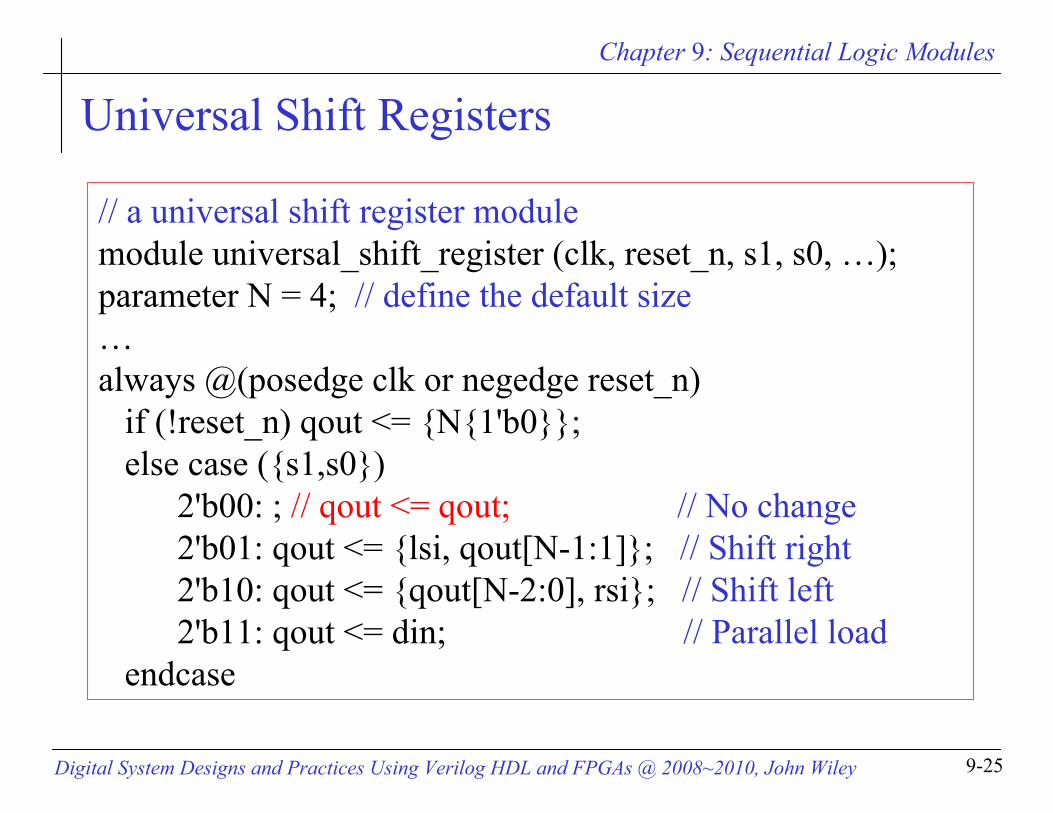
Universal Shift Registers
A universal shift register can carry out SISOSIPOPISOPIPO
The register must have the following capabilitiesParallel loadSerial in and serial outShift left and shift right
Chapter 9: Sequential Logic Modules
Digital System Designs and Practices Using Verilog HDL and FPGAs @ 2008~2010, John Wiley 9-24
Universal Shift Registers
Chapter 9: Sequential Logic Modules
Digital System Designs and Practices Using Verilog HDL and FPGAs @ 2008~2010, John Wiley 9-25
Universal Shift Registers
// a universal shift register modulemodule universal_shift_register (clk, reset_n, s1, s0, …);parameter N = 4; // define the default size …always @(posedge clk or negedge reset_n)
if (!reset_n) qout <= {N{1'b0}};else case ({s1,s0})
2'b00: ; // qout <= qout; // No change 2'b01: qout <= {lsi, qout[N-1:1]}; // Shift right2'b10: qout <= {qout[N-2:0], rsi}; // Shift left2'b11: qout <= din; // Parallel load
endcase
Chapter 9: Sequential Logic Modules
Digital System Designs and Practices Using Verilog HDL and FPGAs @ 2008~2010, John Wiley 9-26
Syllabus
ObjectivesFundamentals of sequential logic modulesFlip-flopsMemory elementsShift registersCountersSequence generatorsTiming generators
Chapter 9: Sequential Logic Modules
Digital System Designs and Practices Using Verilog HDL and FPGAs @ 2008~2010, John Wiley 9-27
Counters
Counter Types
CountersTimers
Chapter 9: Sequential Logic Modules
Digital System Designs and Practices Using Verilog HDL and FPGAs @ 2008~2010, John Wiley 9-28
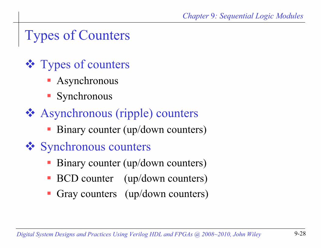
Types of Counters
Types of countersAsynchronousSynchronous
Asynchronous (ripple) countersBinary counter (up/down counters)
Synchronous countersBinary counter (up/down counters)BCD counter (up/down counters)Gray counters (up/down counters)
Chapter 9: Sequential Logic Modules
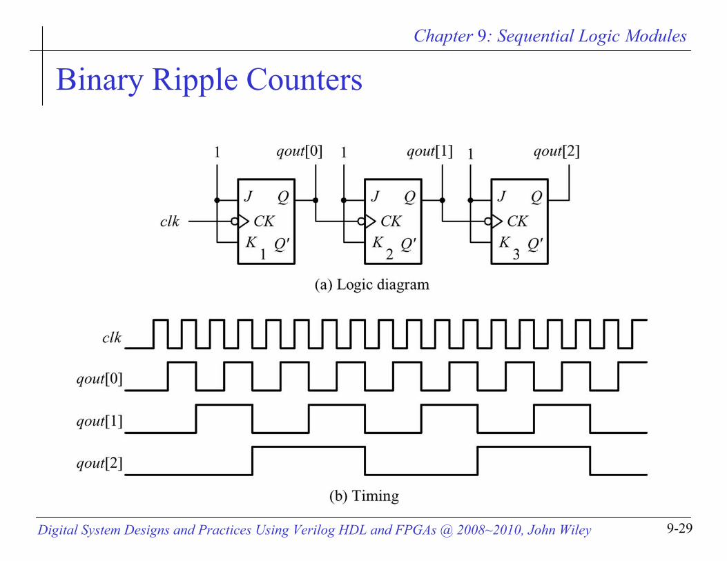
Digital System Designs and Practices Using Verilog HDL and FPGAs @ 2008~2010, John Wiley 9-29
Binary Ripple Counters
Chapter 9: Sequential Logic Modules
Digital System Designs and Practices Using Verilog HDL and FPGAs @ 2008~2010, John Wiley 9-30
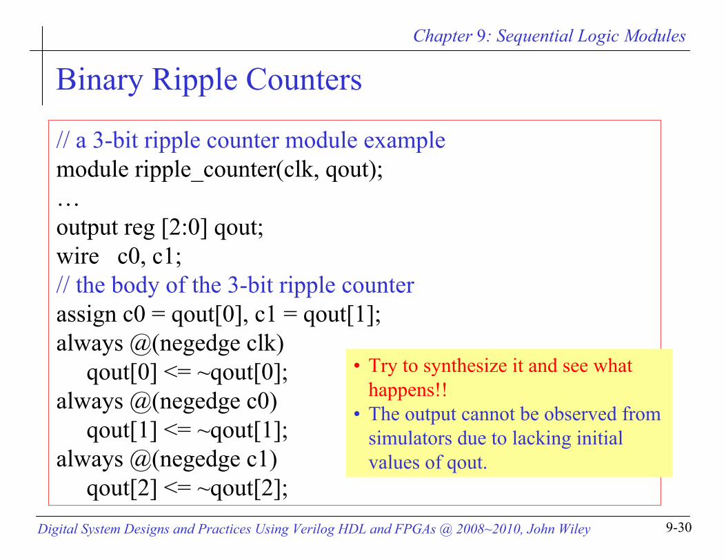
Binary Ripple Counters
// a 3-bit ripple counter module examplemodule ripple_counter(clk, qout);…output reg [2:0] qout;wire c0, c1;// the body of the 3-bit ripple counterassign c0 = qout[0], c1 = qout[1];always @(negedge clk)
qout[0] <= ~qout[0];always @(negedge c0)
qout[1] <= ~qout[1];always @(negedge c1)
qout[2] <= ~qout[2];
• Try to synthesize it and see what happens!!
• The output cannot be observed from simulators due to lacking initial values of qout.
Chapter 9: Sequential Logic Modules
Digital System Designs and Practices Using Verilog HDL and FPGAs @ 2008~2010, John Wiley 9-31
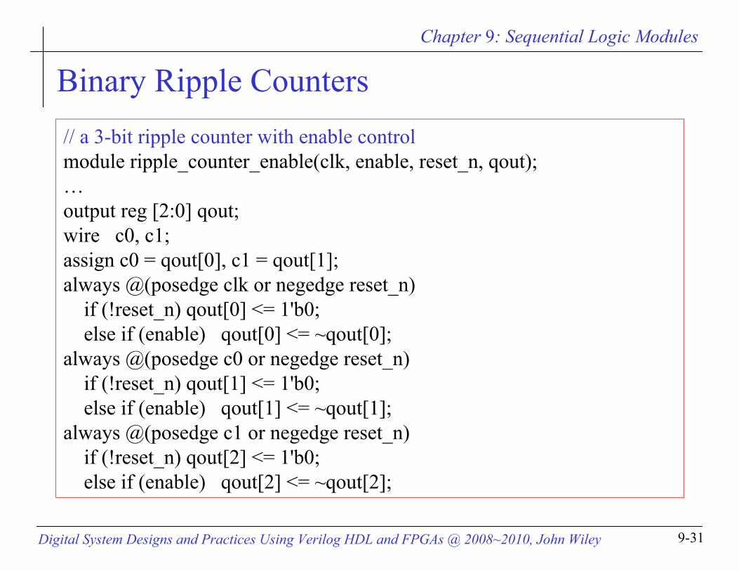
Binary Ripple Counters// a 3-bit ripple counter with enable controlmodule ripple_counter_enable(clk, enable, reset_n, qout);…output reg [2:0] qout;wire c0, c1;assign c0 = qout[0], c1 = qout[1];always @(posedge clk or negedge reset_n)
if (!reset_n) qout[0] <= 1'b0; else if (enable) qout[0] <= ~qout[0];
always @(posedge c0 or negedge reset_n)if (!reset_n) qout[1] <= 1'b0; else if (enable) qout[1] <= ~qout[1];
always @(posedge c1 or negedge reset_n)if (!reset_n) qout[2] <= 1'b0; else if (enable) qout[2] <= ~qout[2];
Chapter 9: Sequential Logic Modules
Digital System Designs and Practices Using Verilog HDL and FPGAs @ 2008~2010, John Wiley 9-32
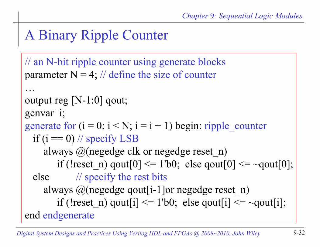
A Binary Ripple Counter
// an N-bit ripple counter using generate blocksparameter N = 4; // define the size of counter…output reg [N-1:0] qout;genvar i;generate for (i = 0; i < N; i = i + 1) begin: ripple_counter
if (i == 0) // specify LSBalways @(negedge clk or negedge reset_n)
if (!reset_n) qout[0] <= 1'b0; else qout[0] <= ~qout[0];else // specify the rest bits
always @(negedge qout[i-1]or negedge reset_n) if (!reset_n) qout[i] <= 1'b0; else qout[i] <= ~qout[i];
end endgenerate
Chapter 9: Sequential Logic Modules
Digital System Designs and Practices Using Verilog HDL and FPGAs @ 2008~2010, John Wiley 9-33
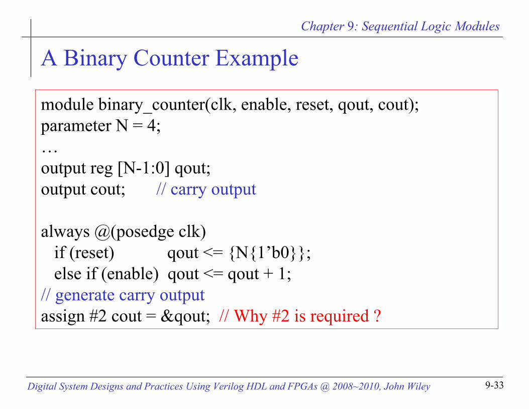
A Binary Counter Example
module binary_counter(clk, enable, reset, qout, cout);parameter N = 4;…output reg [N-1:0] qout;output cout; // carry output
always @(posedge clk)if (reset) qout <= {N{1’b0}};else if (enable) qout <= qout + 1;
// generate carry outputassign #2 cout = &qout; // Why #2 is required ?
Chapter 9: Sequential Logic Modules
Digital System Designs and Practices Using Verilog HDL and FPGAs @ 2008~2010, John Wiley 9-34
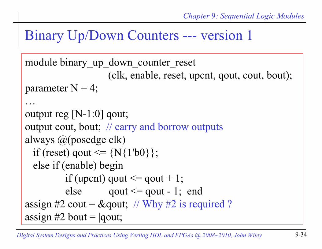
Binary Up/Down Counters --- version 1
module binary_up_down_counter_reset(clk, enable, reset, upcnt, qout, cout, bout);
parameter N = 4;…output reg [N-1:0] qout;output cout, bout; // carry and borrow outputsalways @(posedge clk)
if (reset) qout <= {N{1'b0}};else if (enable) begin
if (upcnt) qout <= qout + 1;else qout <= qout - 1; end
assign #2 cout = &qout; // Why #2 is required ?assign #2 bout = |qout;
Chapter 9: Sequential Logic Modules
Digital System Designs and Practices Using Verilog HDL and FPGAs @ 2008~2010, John Wiley 9-35
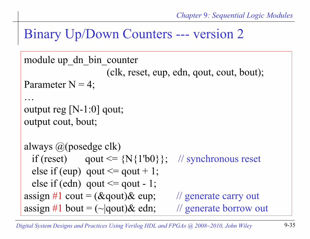
Binary Up/Down Counters --- version 2
module up_dn_bin_counter(clk, reset, eup, edn, qout, cout, bout);
Parameter N = 4;…output reg [N-1:0] qout;output cout, bout;
always @(posedge clk)if (reset) qout <= {N{1'b0}}; // synchronous resetelse if (eup) qout <= qout + 1;else if (edn) qout <= qout - 1;
assign #1 cout = (&qout)& eup; // generate carry outassign #1 bout = (~|qout)& edn; // generate borrow out
Chapter 9: Sequential Logic Modules
Digital System Designs and Practices Using Verilog HDL and FPGAs @ 2008~2010, John Wiley 9-36
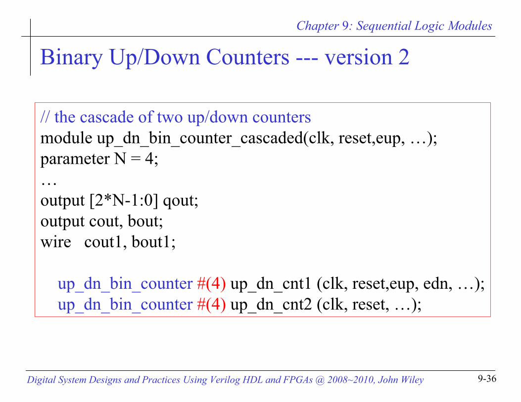
Binary Up/Down Counters --- version 2
// the cascade of two up/down countersmodule up_dn_bin_counter_cascaded(clk, reset,eup, …);parameter N = 4;…output [2*N-1:0] qout;output cout, bout;wire cout1, bout1;
up_dn_bin_counter #(4) up_dn_cnt1 (clk, reset,eup, edn, …);up_dn_bin_counter #(4) up_dn_cnt2 (clk, reset, …);
Chapter 9: Sequential Logic Modules
Digital System Designs and Practices Using Verilog HDL and FPGAs @ 2008~2010, John Wiley 9-37
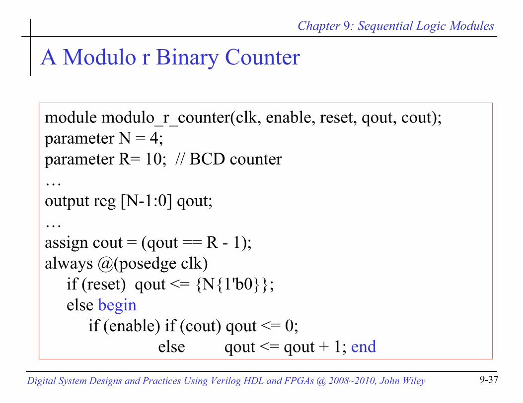
A Modulo r Binary Counter
module modulo_r_counter(clk, enable, reset, qout, cout);parameter N = 4;parameter R= 10; // BCD counter…output reg [N-1:0] qout;…assign cout = (qout == R - 1);always @(posedge clk)
if (reset) qout <= {N{1'b0}};else begin
if (enable) if (cout) qout <= 0;else qout <= qout + 1; end
Chapter 9: Sequential Logic Modules
Digital System Designs and Practices Using Verilog HDL and FPGAs @ 2008~2010, John Wiley 9-38
Syllabus
ObjectivesFundamentals of sequential logic modulesFlip-flopsMemory elementsShift registersCountersSequence generatorsTiming generators
Chapter 9: Sequential Logic Modules
Digital System Designs and Practices Using Verilog HDL and FPGAs @ 2008~2010, John Wiley 9-39
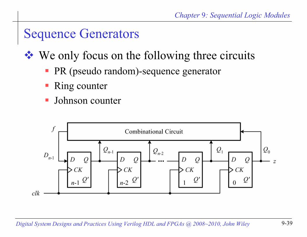
Sequence GeneratorsWe only focus on the following three circuits
PR (pseudo random)-sequence generatorRing counterJohnson counter
Chapter 9: Sequential Logic Modules
Digital System Designs and Practices Using Verilog HDL and FPGAs @ 2008~2010, John Wiley 9-40
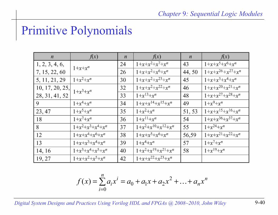
Primitive Polynomials
nn
n
i
ii xaxaxaaxaxf ++++== ∑
=…2
2100
)(
Chapter 9: Sequential Logic Modules
Digital System Designs and Practices Using Verilog HDL and FPGAs @ 2008~2010, John Wiley 9-41
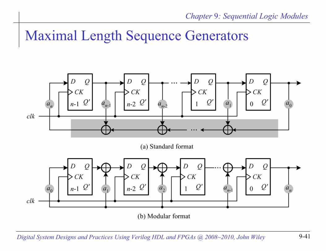
Maximal Length Sequence Generators
Chapter 9: Sequential Logic Modules
Digital System Designs and Practices Using Verilog HDL and FPGAs @ 2008~2010, John Wiley 9-42
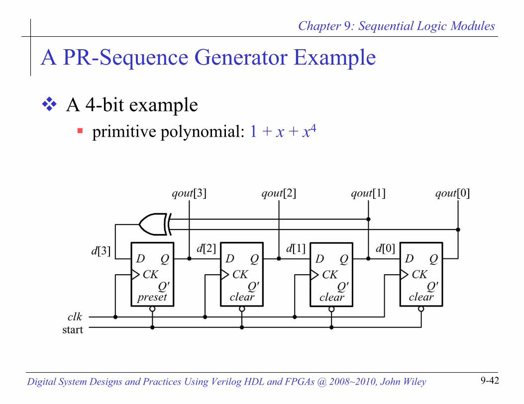
A PR-Sequence Generator Example
A 4-bit exampleprimitive polynomial: 1 + x + x4
Chapter 9: Sequential Logic Modules
Digital System Designs and Practices Using Verilog HDL and FPGAs @ 2008~2010, John Wiley 9-43
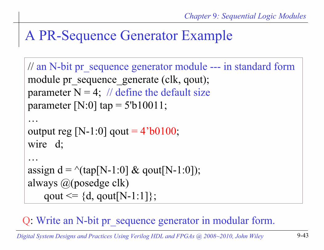
A PR-Sequence Generator Example
// an N-bit pr_sequence generator module --- in standard formmodule pr_sequence_generate (clk, qout);parameter N = 4; // define the default sizeparameter [N:0] tap = 5'b10011;…output reg [N-1:0] qout = 4’b0100; wire d; …assign d = ^(tap[N-1:0] & qout[N-1:0]);always @(posedge clk)
qout <= {d, qout[N-1:1]};
Q: Write an N-bit pr_sequence generator in modular form.
Chapter 9: Sequential Logic Modules
Digital System Designs and Practices Using Verilog HDL and FPGAs @ 2008~2010, John Wiley 9-44
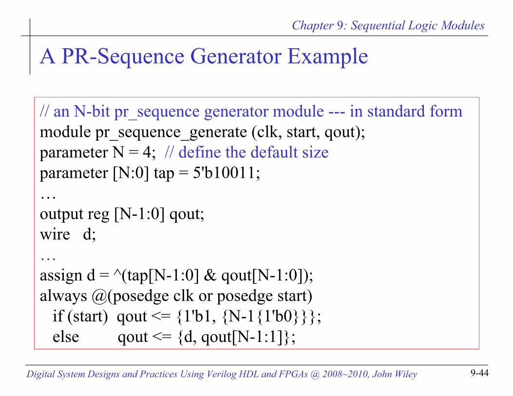
A PR-Sequence Generator Example
// an N-bit pr_sequence generator module --- in standard formmodule pr_sequence_generate (clk, start, qout);parameter N = 4; // define the default size parameter [N:0] tap = 5'b10011;…output reg [N-1:0] qout;wire d;…assign d = ^(tap[N-1:0] & qout[N-1:0]);always @(posedge clk or posedge start)
if (start) qout <= {1'b1, {N-1{1'b0}}};else qout <= {d, qout[N-1:1]};
Chapter 9: Sequential Logic Modules
Digital System Designs and Practices Using Verilog HDL and FPGAs @ 2008~2010, John Wiley 9-45
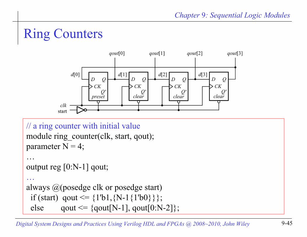
Ring Counters
// a ring counter with initial valuemodule ring_counter(clk, start, qout);parameter N = 4;…output reg [0:N-1] qout;…always @(posedge clk or posedge start)if (start) qout <= {1'b1,{N-1{1'b0}}};else qout <= {qout[N-1], qout[0:N-2]};
Chapter 9: Sequential Logic Modules
Digital System Designs and Practices Using Verilog HDL and FPGAs @ 2008~2010, John Wiley 9-46
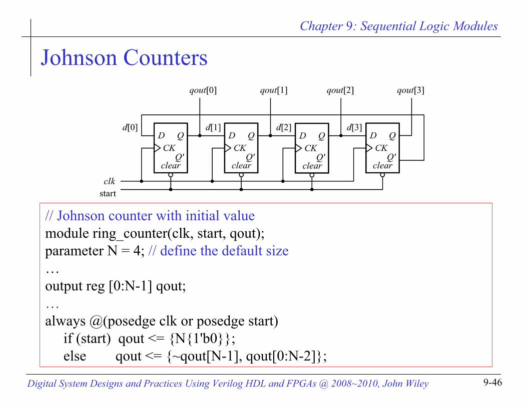
Johnson Counters
// Johnson counter with initial valuemodule ring_counter(clk, start, qout);parameter N = 4; // define the default size…output reg [0:N-1] qout;…always @(posedge clk or posedge start)
if (start) qout <= {N{1'b0}};else qout <= {~qout[N-1], qout[0:N-2]};
Chapter 9: Sequential Logic Modules
Digital System Designs and Practices Using Verilog HDL and FPGAs @ 2008~2010, John Wiley 9-47
Syllabus
ObjectivesFundamentals of sequential logic modulesFlip-flopsMemory elementsShift registersCountersSequence generatorsTiming generators
Chapter 9: Sequential Logic Modules
Digital System Designs and Practices Using Verilog HDL and FPGAs @ 2008~2010, John Wiley 9-48
Timing Generators
A timing generator Multiphase clock signals
Ring counterBinary counter with decoder
Digital monostable circuitsRetriggerableNonretriggerable
Chapter 9: Sequential Logic Modules
Digital System Designs and Practices Using Verilog HDL and FPGAs @ 2008~2010, John Wiley 9-49
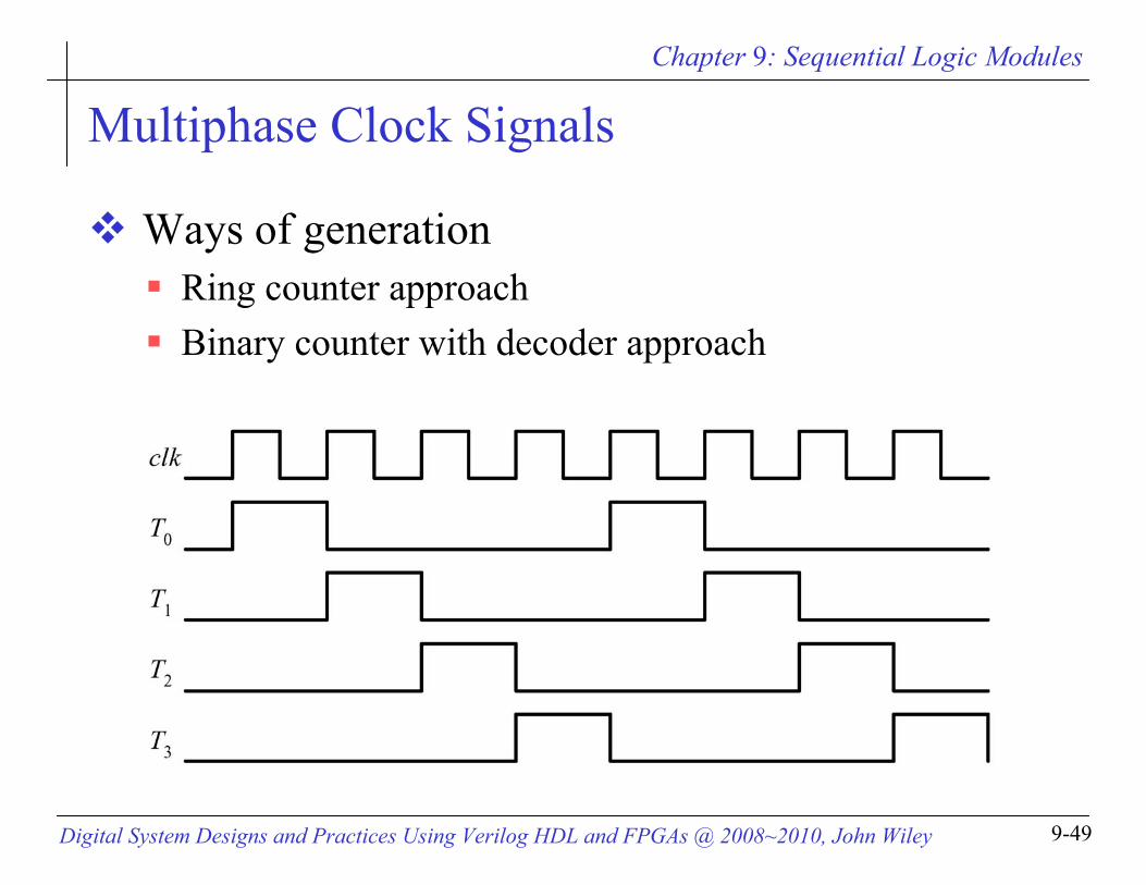
Multiphase Clock Signals
Ways of generation Ring counter approachBinary counter with decoder approach
Chapter 9: Sequential Logic Modules
Digital System Designs and Practices Using Verilog HDL and FPGAs @ 2008~2010, John Wiley 9-50
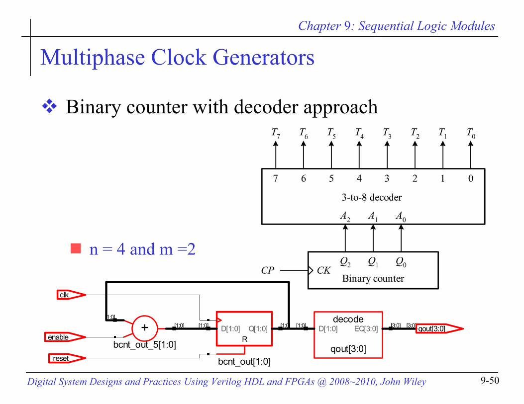
Multiphase Clock Generators
Binary counter with decoder approach
decode
qout[3:0] bcnt_out_5[1:0] +
bcnt_out[1:0]
R
[3:0]EQ[3:0][1:0] D[1:0][1:0]
[1:0] [1:0]Q[1:0][1:0] D[1:0] qout[3:0][3:0]
enable
reset
clk
n = 4 and m =2
Chapter 9: Sequential Logic Modules
Digital System Designs and Practices Using Verilog HDL and FPGAs @ 2008~2010, John Wiley 9-51
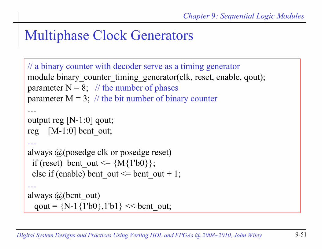
Multiphase Clock Generators
// a binary counter with decoder serve as a timing generatormodule binary_counter_timing_generator(clk, reset, enable, qout);parameter N = 8; // the number of phasesparameter M = 3; // the bit number of binary counter…output reg [N-1:0] qout;reg [M-1:0] bcnt_out;…always @(posedge clk or posedge reset)if (reset) bcnt_out <= {M{1'b0}};else if (enable) bcnt_out <= bcnt_out + 1;
…always @(bcnt_out)
qout = {N-1{1'b0},1'b1} << bcnt_out;


