1
Hardware and The Memory Hierarchy
Andrew Case
Slides adapted from Jinjang Li, Mohamed Zahran, Randy Bryant and Dave O’Hallaron
2
Topics System Hardware
Chipsets Buses I/O devices Memory
Storage technologies and trends Locality of reference Caching in the memory hierarchy

3
System Board (i.e. motherboard)Memory slots
1 PCIe expansion slot(graphics, etc.)
CPU socket
Chipset provides bus interface between devices including
CPU, sound, network, graphics,
etc.
ExternalI/O Ports(mouse, network,
etc.)
Power connector
Internal I/O Ports
(Flash/Disk drives)
4
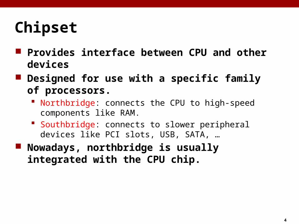
Chipset Provides interface between CPU and other devices Designed for use with a specific family of processors.
Northbridge: connects the CPU to high-speed components like RAM.
Southbridge: connects to slower peripheral devices like PCI slots, USB, SATA, …
Nowadays, northbridge is usually integrated with the CPU chip.
5
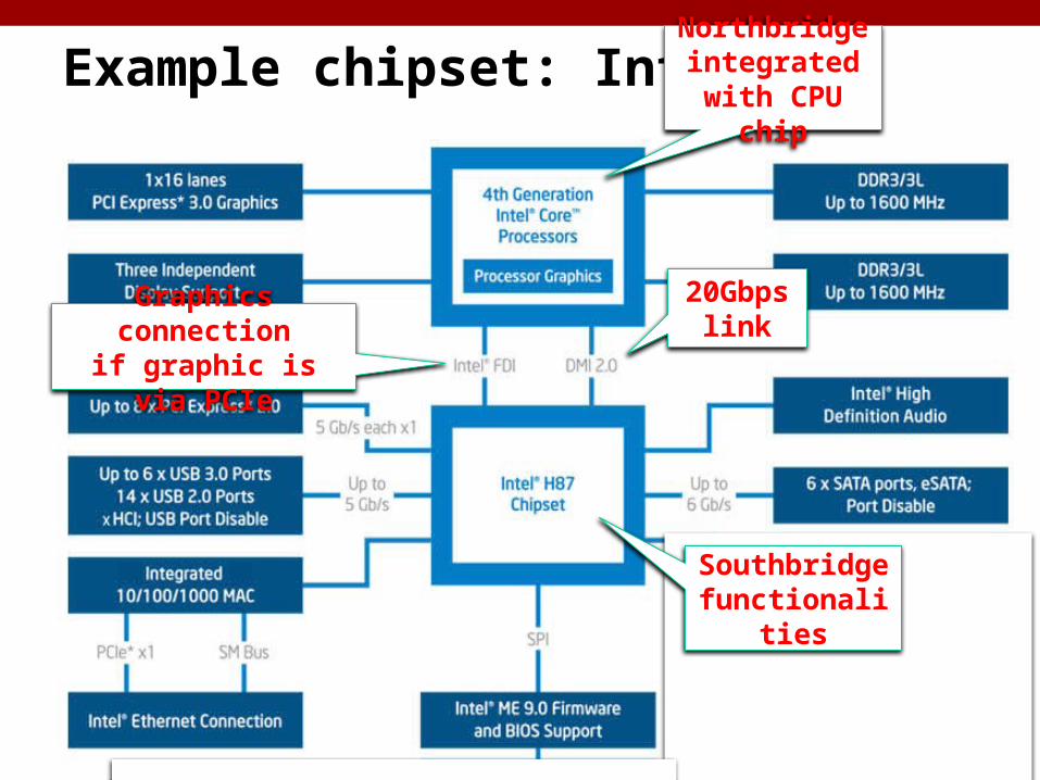
Example chipset: Intel H87 Northbridge integrated with
CPU chip
Southbridge functionalities
20GbpslinkGraphics connection
if graphic is via PCIe
6
Buses
• Connect components together Most buses use common protocols for interoperability
• A bus carries address, data, and control lines. • Common buses:
Memory bus PCI bus SATA Universal serial bus (USB) System management bus (SM)
7
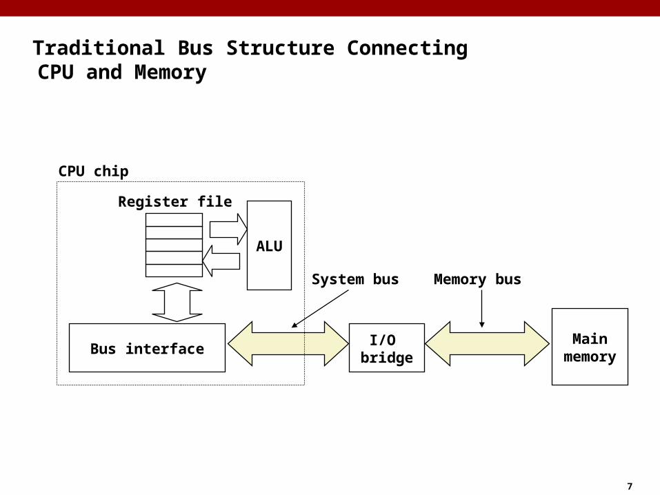
Traditional Bus Structure Connecting CPU and Memory
Mainmemory
I/O bridge
Bus interface
ALU
Register file
CPU chip
System bus Memory bus
8
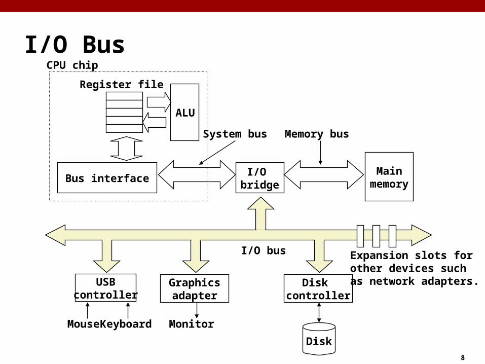
I/O Bus
Mainmemory
I/O bridge
Bus interface
ALU
Register file
CPU chip
System bus Memory bus
Disk controller
Graphicsadapter
USBcontroller
Mouse Keyboard Monitor
Disk
I/O bus Expansion slots forother devices suchas network adapters.
9
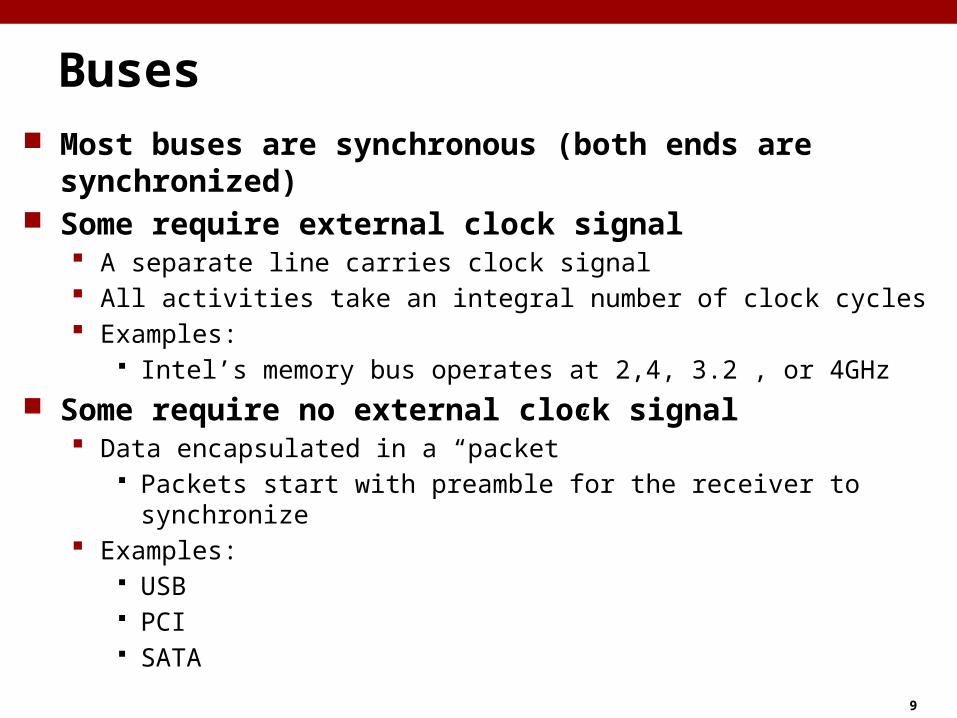
Buses Most buses are synchronous (both ends are synchronized) Some require external clock signal
A separate line carries clock signal All activities take an integral number of clock cycles Examples:
Intel’s memory bus operates at 2,4, 3.2 , or 4GHz Some require no external clock signal
Data encapsulated in a “packet” Packets start with preamble for the receiver to synchronize
Examples: USB PCI SATA
10
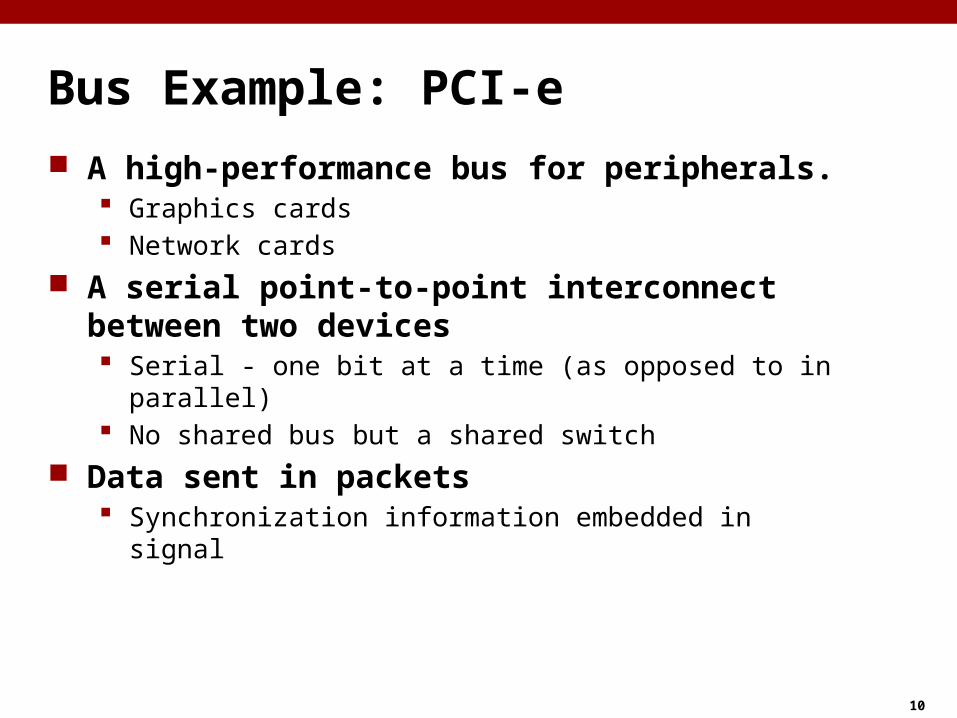
Bus Example: PCI-e A high-performance bus for peripherals.
Graphics cards Network cards
A serial point-to-point interconnect between two devices Serial - one bit at a time (as opposed to in parallel) No shared bus but a shared switch
Data sent in packets Synchronization information embedded in signal
11
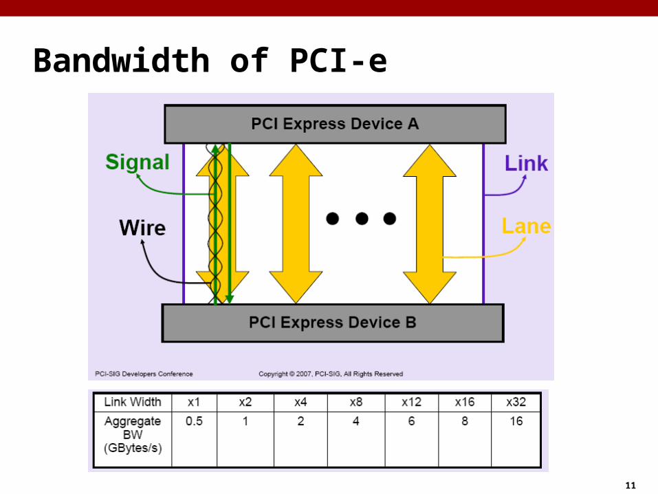
Bandwidth of PCI-e
12
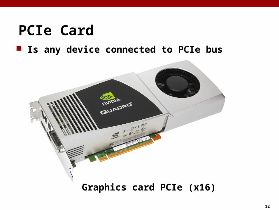
Is any device connected to PCIe bus
Graphics card PCIe (x16)
PCIe Card
13
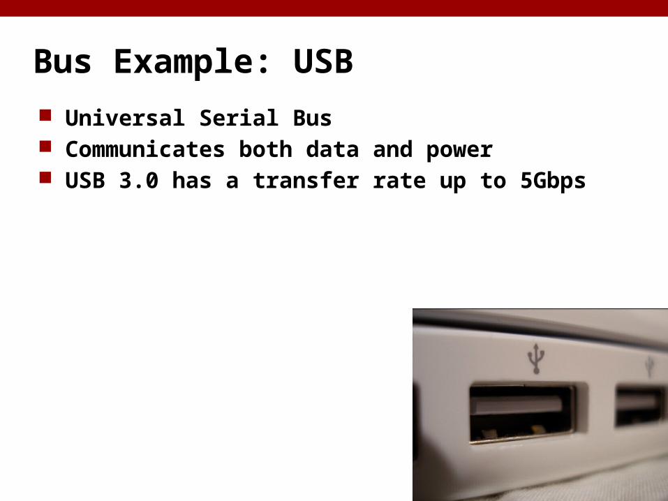
Bus Example: USB Universal Serial Bus Communicates both data and power USB 3.0 has a transfer rate up to 5Gbps
14
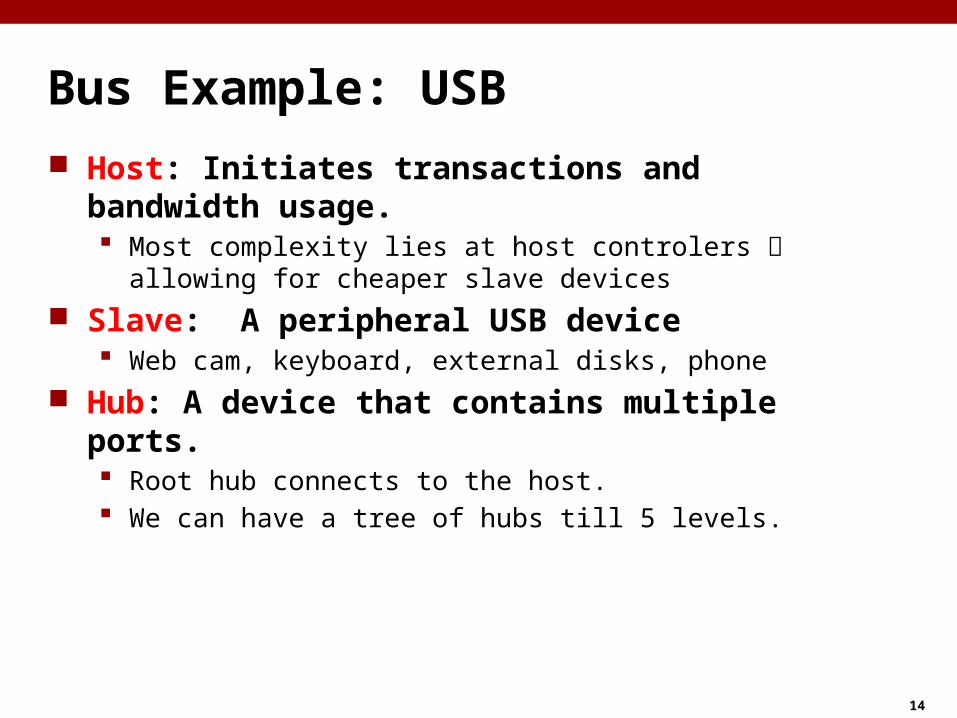
Bus Example: USB Host: Initiates transactions and bandwidth usage.
Most complexity lies at host controlers allowing for cheaper slave devices
Slave: A peripheral USB device Web cam, keyboard, external disks, phone
Hub: A device that contains multiple ports. Root hub connects to the host. We can have a tree of hubs till 5 levels.
15
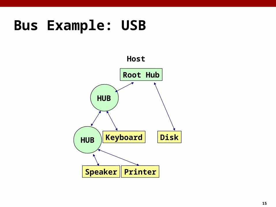
Bus Example: USB
Host
HUB
HUB
Root Hub
Keyboard
Speaker
Disk
Printer
16
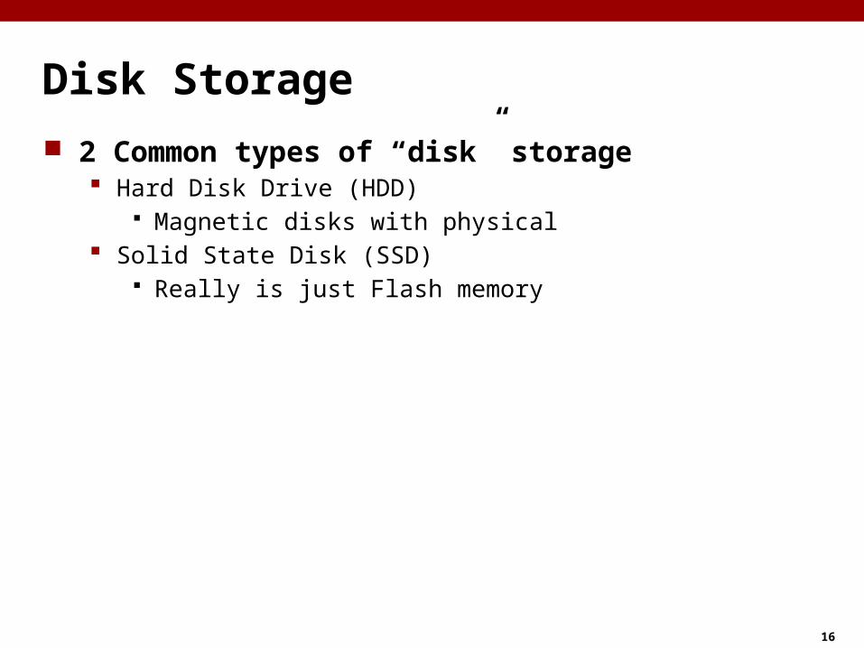
Disk Storage 2 Common types of “disk” storage
Hard Disk Drive (HDD) Magnetic disks with physical
Solid State Disk (SSD) Really is just Flash memory
17
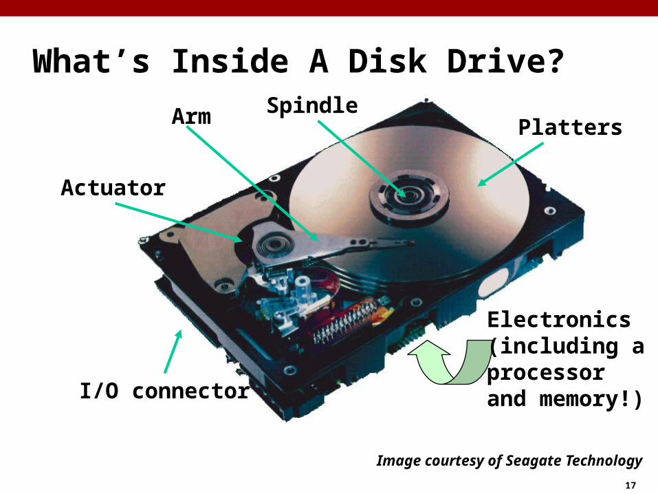
What’s Inside A Disk Drive?SpindleArm
Actuator
Platters
Electronics(including a processor and memory!)I/O connector
Image courtesy of Seagate Technology
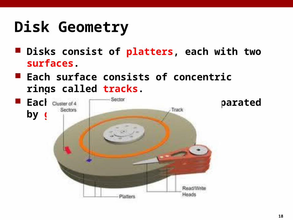
18
Disk Geometry Disks consist of platters, each with two surfaces. Each surface consists of concentric rings called tracks. Each track consists of sectors separated by gaps.
19
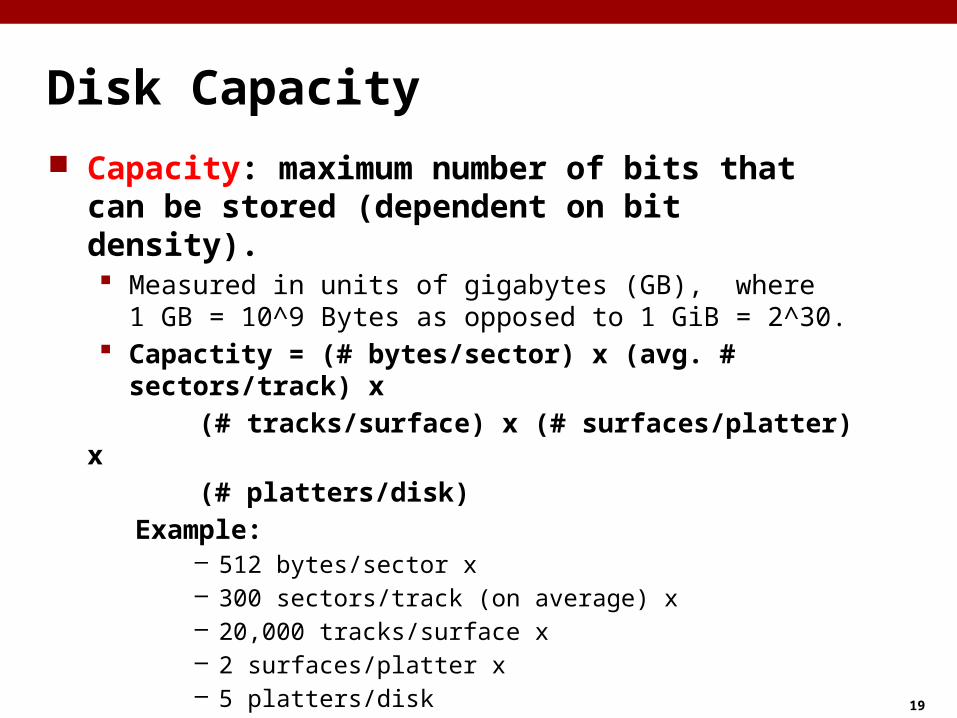
Disk Capacity Capacity: maximum number of bits that can be stored
(dependent on bit density). Measured in units of gigabytes (GB), where
1 GB = 10^9 Bytes as opposed to 1 GiB = 2^30. Capactity = (# bytes/sector) x (avg. # sectors/track) x
(# tracks/surface) x (# surfaces/platter) x (# platters/disk)
Example:– 512 bytes/sector x– 300 sectors/track (on average) x– 20,000 tracks/surface x– 2 surfaces/platter x– 5 platters/disk
Capacity = 512 x 300 x 20000 x 2 x 5 = 30,720,000,000 Bytes = 30.72 GB ~= 28.6GiB

20
Disk Operation (Single-Platter View)
The disk surface spins at a fixedrotational rate
By moving radially, the arm can position the read/write head over any track.
The read/write headis attached to the endof the arm and flies over the disk surface ona thin cushion of air.
spindle
spindle
spin
dle
spindlespindle
21
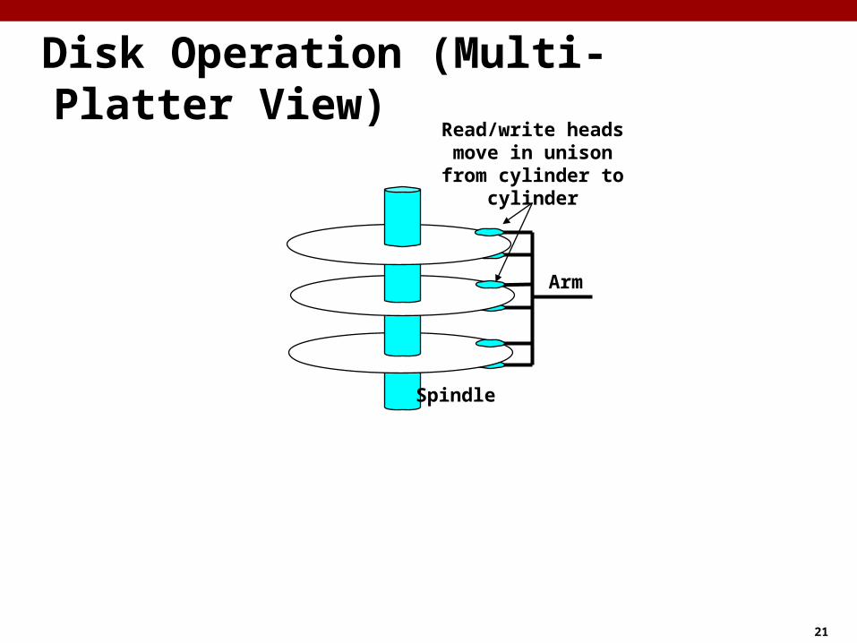
Disk Operation (Multi-Platter View)
Arm
Read/write heads move in unison
from cylinder to cylinder
Spindle
22
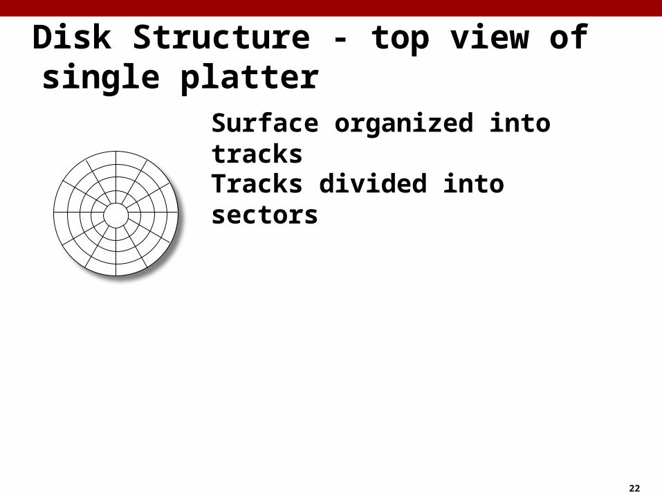
Tracks divided into sectors
Disk Structure - top view of single platter
Surface organized into tracks
23
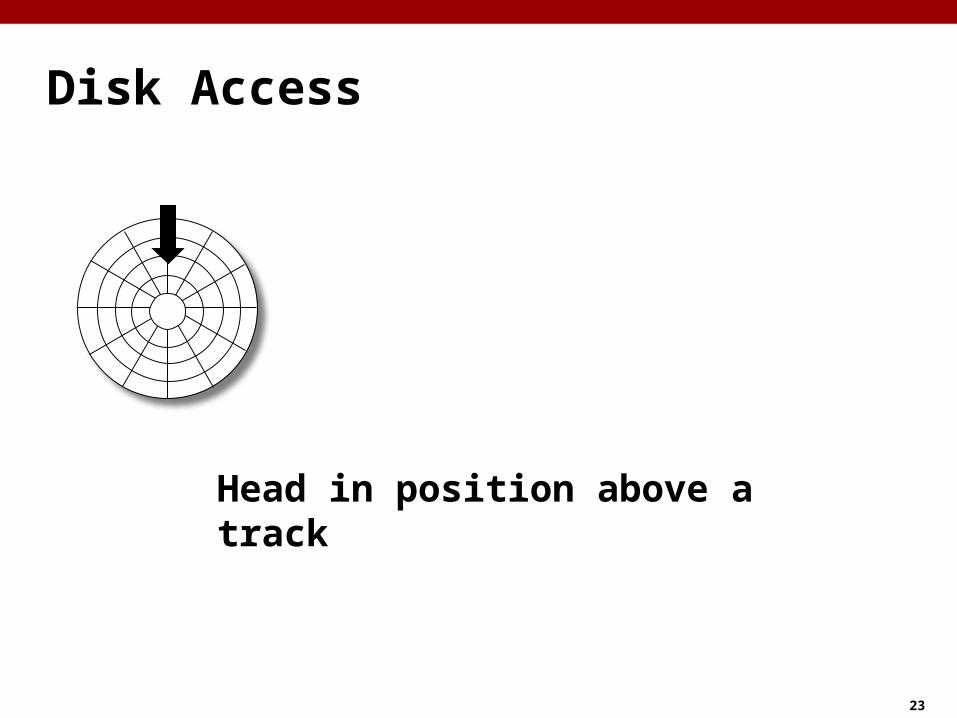
Disk Access
Head in position above a track
24
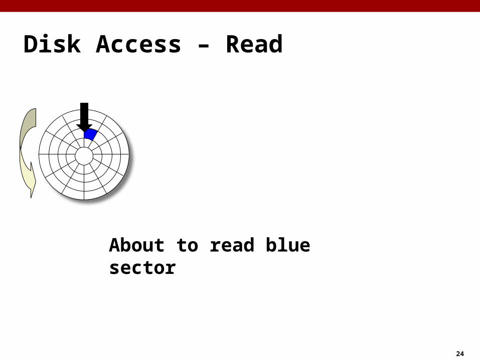
Disk Access – Read
About to read blue sector
25
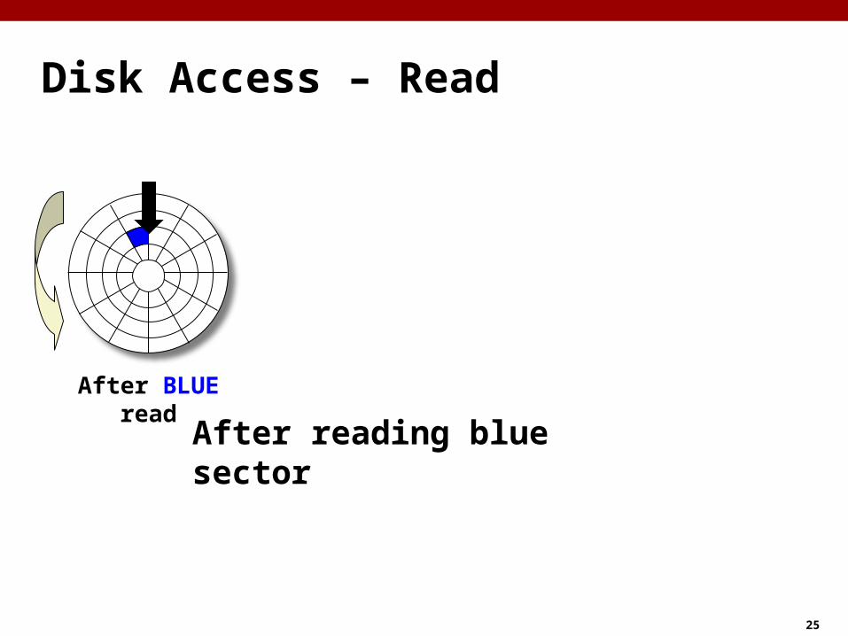
Disk Access – Read
After BLUE read
After reading blue sector
26
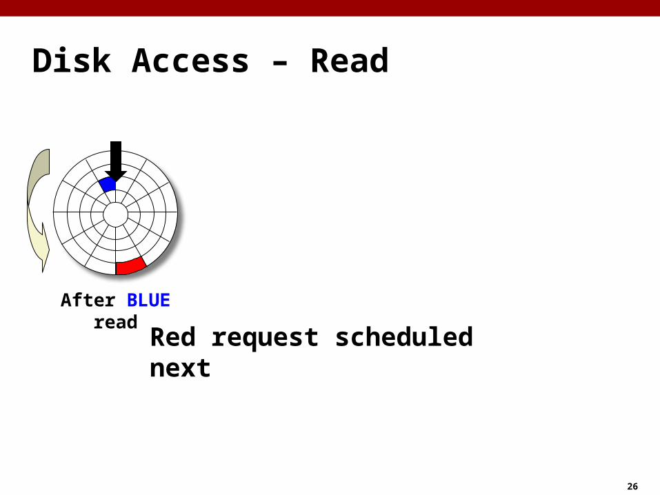
Disk Access – Read
After BLUE read
Red request scheduled next
27
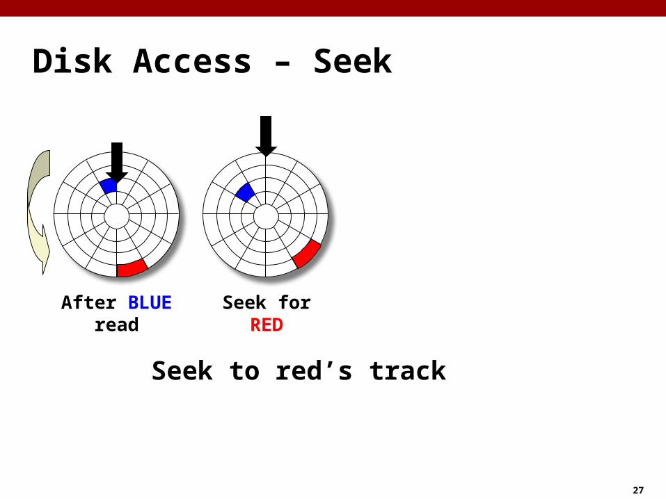
Disk Access – Seek
After BLUE read Seek for RED
Seek to red’s track
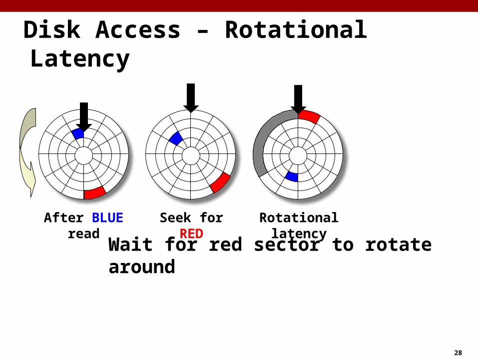
28
Disk Access – Rotational Latency
After BLUE read Seek for RED Rotational latency
Wait for red sector to rotate around
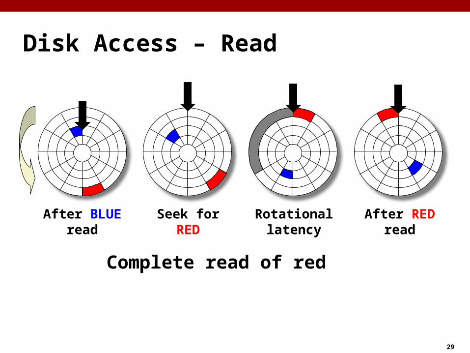
29
Disk Access – Read
After BLUE read Seek for RED Rotational latency After RED read
Complete read of red
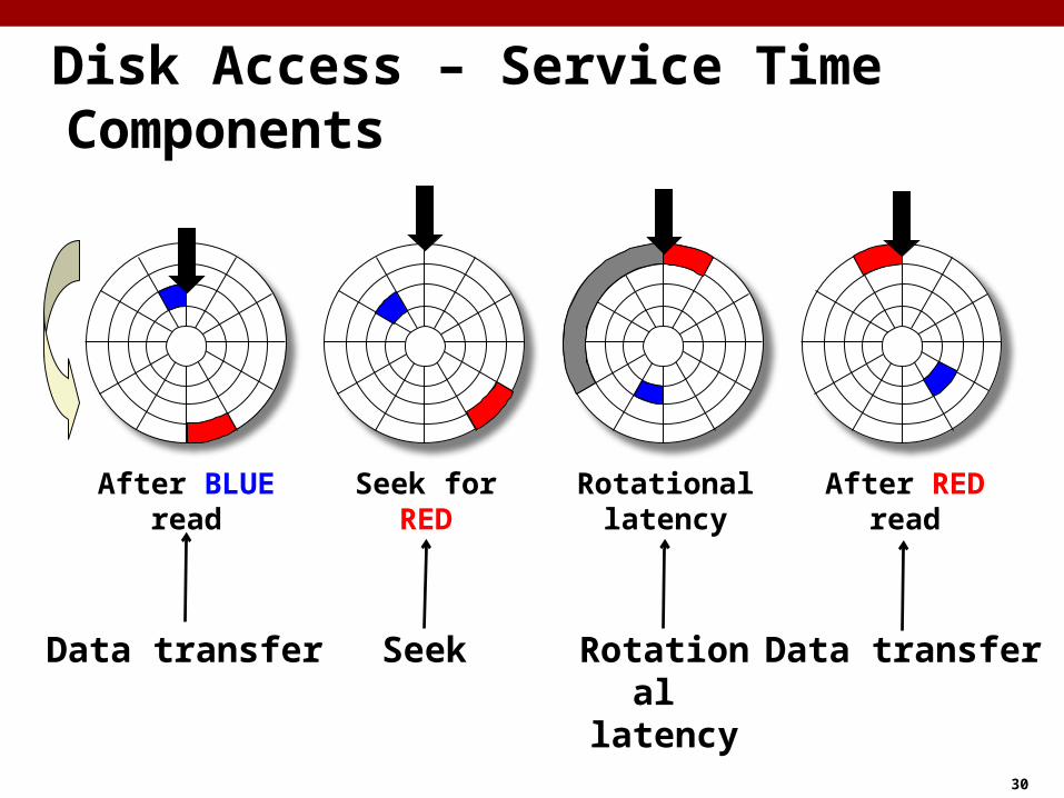
30
Disk Access – Service Time Components
After BLUE read Seek for RED Rotational latency After RED read
Data transfer Seek Rotational latency
Data transfer
31
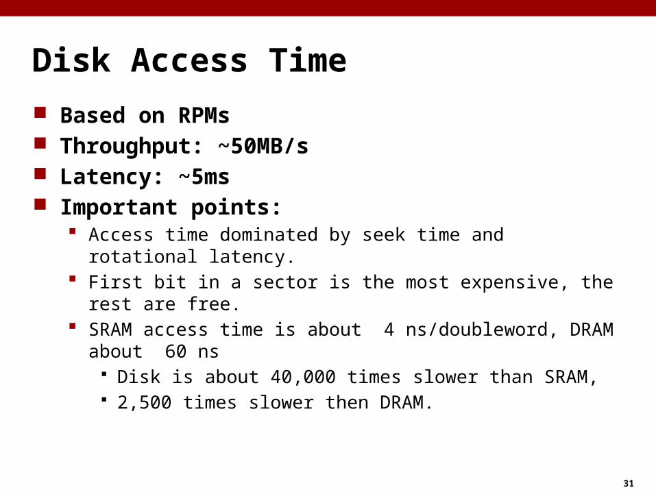
Disk Access Time Based on RPMs Throughput: ~50MB/s Latency: ~5ms Important points:
Access time dominated by seek time and rotational latency. First bit in a sector is the most expensive, the rest are free. SRAM access time is about 4 ns/doubleword, DRAM about 60 ns
Disk is about 40,000 times slower than SRAM, 2,500 times slower then DRAM.
32
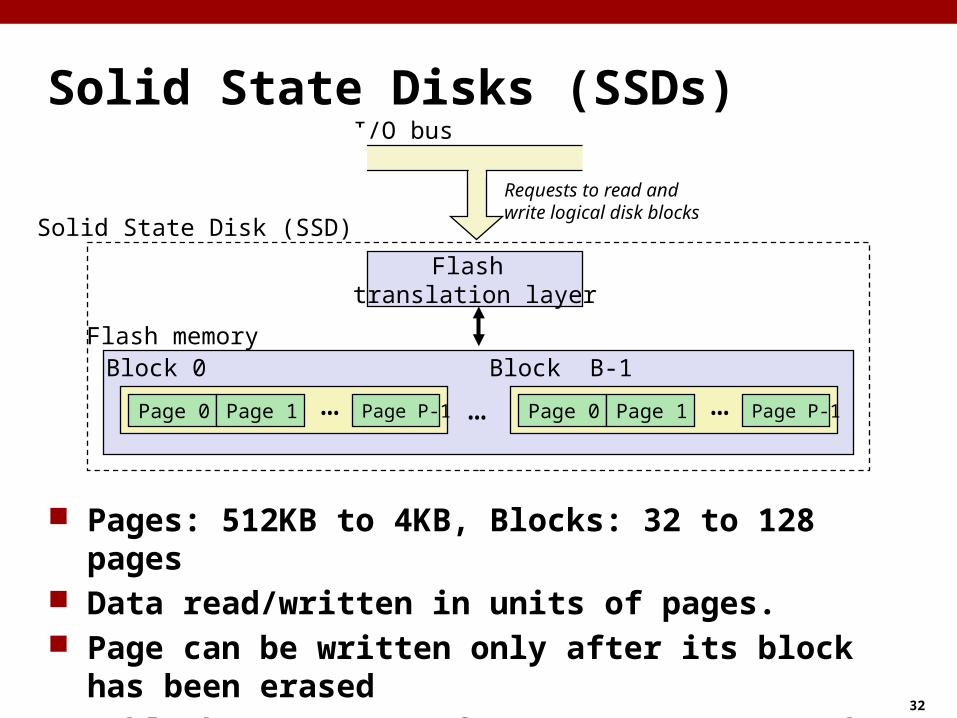
Solid State Disks (SSDs)
Pages: 512KB to 4KB, Blocks: 32 to 128 pages Data read/written in units of pages. Page can be written only after its block has been erased A block wears out after 100,000 repeated writes.
Flash translation layer
I/O bus
Page 0 Page 1 Page P-1…Block 0
… Page 0 Page 1 Page P-1…Block B-1
Flash memory
Solid State Disk (SSD)
Requests to read and write logical disk blocks
33
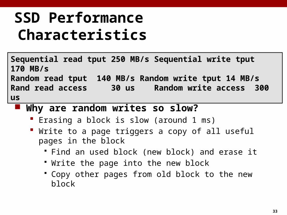
SSD Performance Characteristics
Why are random writes so slow? Erasing a block is slow (around 1 ms) Write to a page triggers a copy of all useful pages in the block
Find an used block (new block) and erase it Write the page into the new block Copy other pages from old block to the new block
Sequential read tput 250 MB/s Sequential write tput 170 MB/sRandom read tput 140 MB/s Random write tput 14 MB/sRand read access 30 us Random write access 300 us

34
SSD Tradeoffs vs. HDD (Hard Disk Drives) Advantages
No moving parts faster, less power, more rugged Disadvantages
Have the potential to wear out (so do HDDs) Mitigated by “wear leveling logic” in flash translation layer E.g. Intel X25 guarantees 1 petabyte (1015 bytes) of random
writes before they wear out In 2010, about 100x more expensive per byte In 2014, about 3x more expensive per byte
Applications MP3 players, smart phones, laptops Becoming more standard in desktops and servers

35
I/O Bus
Mainmemory
I/O bridge
Bus interface
ALU
Register file
CPU chip
System bus Memory bus
Disk controller
Graphicsadapter
USBcontroller
Mouse Keyboard Monitor
Disk
I/O bus Expansion slots forother devices suchas network adapters.
36
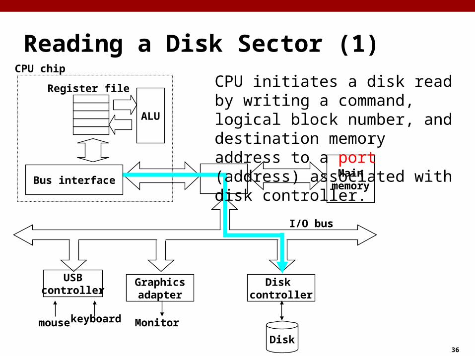
Reading a Disk Sector (1)
Mainmemory
ALU
Register file
CPU chip
Disk controller
Graphicsadapter
USBcontroller
mouse keyboard Monitor
Disk
I/O bus
Bus interface
CPU initiates a disk read by writing a command, logical block number, and destination memory address to a port (address) associated with disk controller.
37
Reading a Disk Sector (2)
Mainmemory
ALU
Register file
CPU chip
Disk controller
Graphicsadapter
USBcontroller
Mouse Keyboard Monitor
Disk
I/O bus
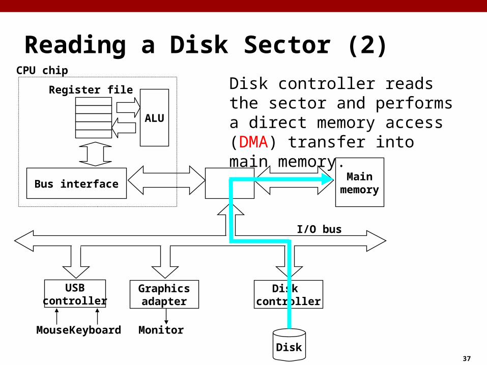
Bus interface
Disk controller reads the sector and performs a direct memory access (DMA) transfer into main memory.
38
Reading a Disk Sector (3)
Mainmemory
ALU
Register file
CPU chip
Disk controller
Graphicsadapter
USBcontroller
Mouse Keyboard Monitor
Disk
I/O bus
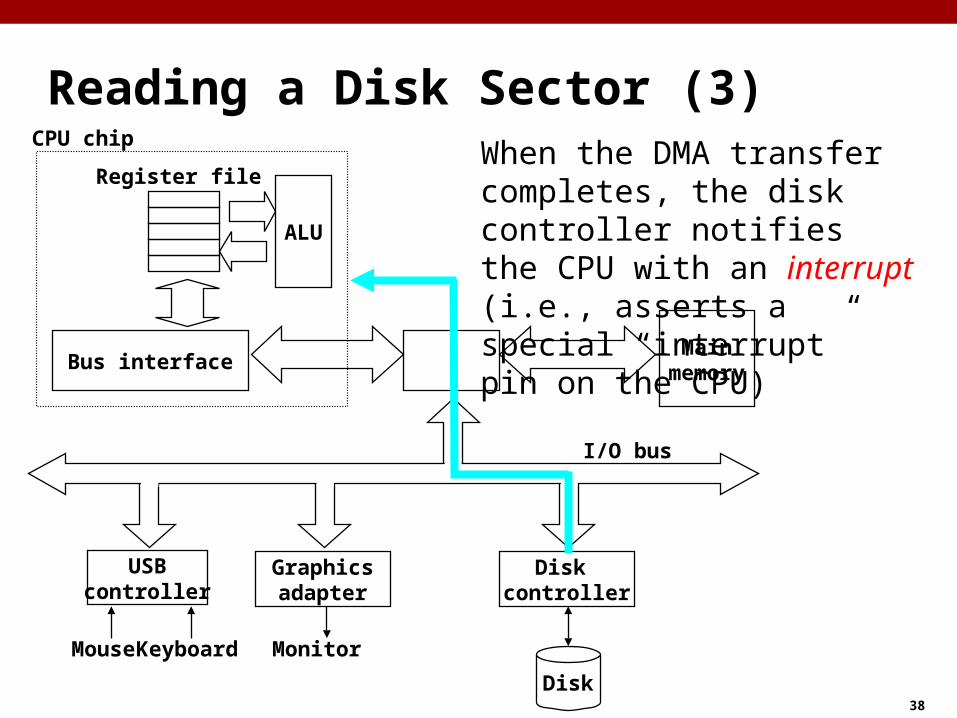
Bus interface
When the DMA transfer completes, the disk controller notifies the CPU with an interrupt (i.e., asserts a special “interrupt” pin on the CPU)
39
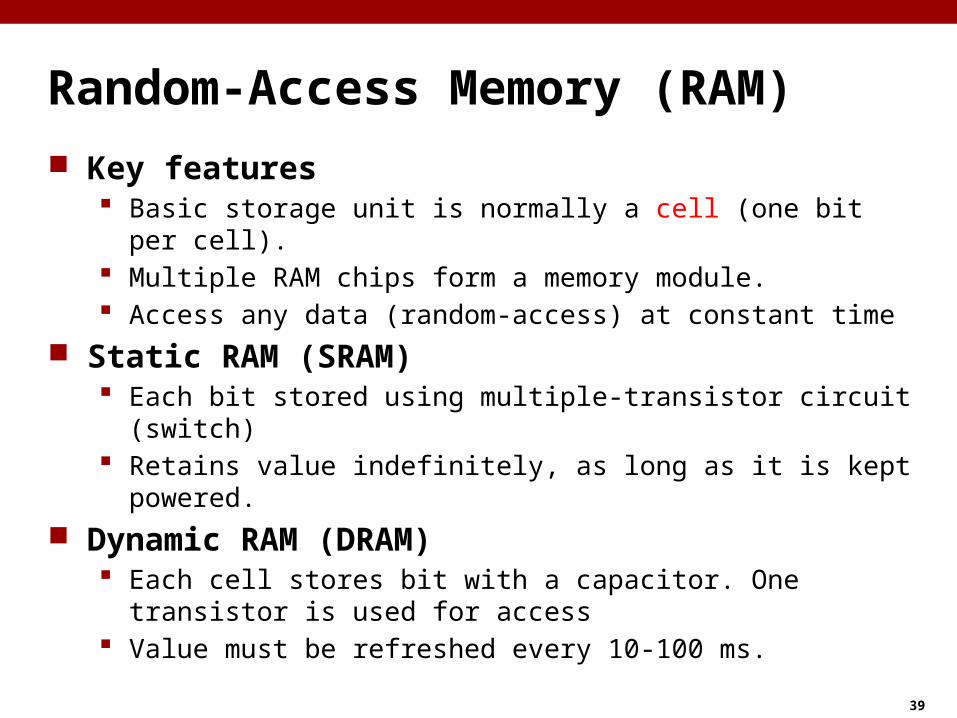
Random-Access Memory (RAM) Key features
Basic storage unit is normally a cell (one bit per cell). Multiple RAM chips form a memory module. Access any data (random-access) at constant time
Static RAM (SRAM) Each bit stored using multiple-transistor circuit (switch) Retains value indefinitely, as long as it is kept powered.
Dynamic RAM (DRAM) Each cell stores bit with a capacitor. One transistor is used for access Value must be refreshed every 10-100 ms.
40
SRAM vs DRAM Summary
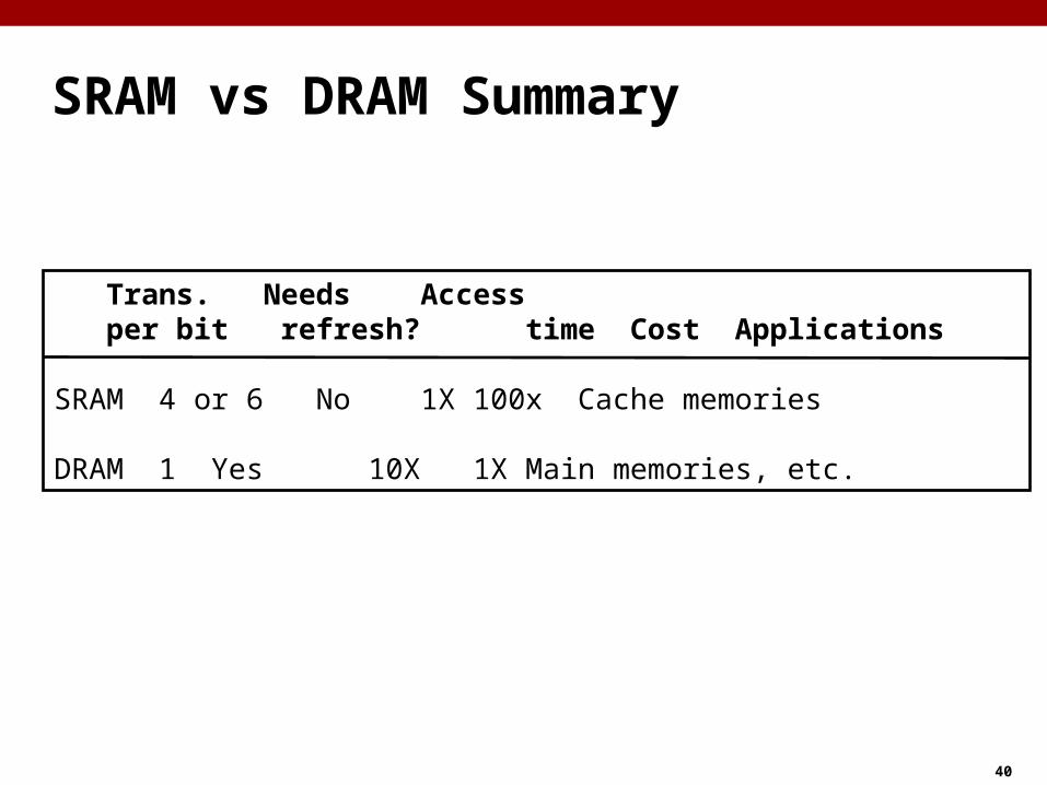
Trans. Needs Accessper bit refresh? time Cost Applications
SRAM 4 or 6 No 1X 100x Cache memories
DRAM 1 Yes 10X 1X Main memories, etc.
41
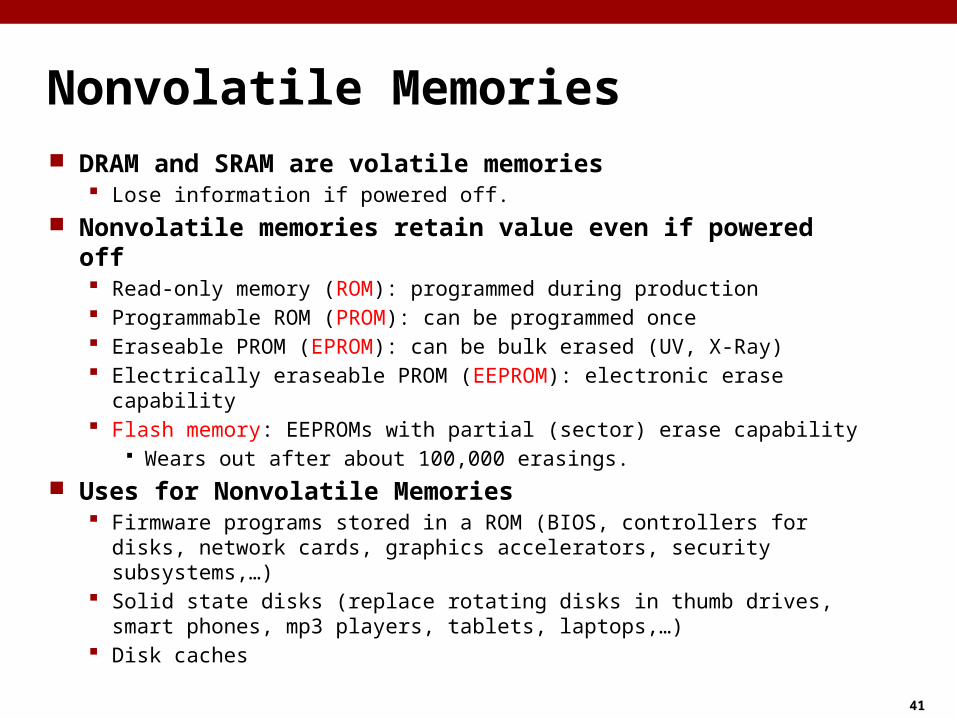
Nonvolatile Memories DRAM and SRAM are volatile memories
Lose information if powered off. Nonvolatile memories retain value even if powered off
Read-only memory (ROM): programmed during production Programmable ROM (PROM): can be programmed once Eraseable PROM (EPROM): can be bulk erased (UV, X-Ray) Electrically eraseable PROM (EEPROM): electronic erase capability Flash memory: EEPROMs with partial (sector) erase capability
Wears out after about 100,000 erasings. Uses for Nonvolatile Memories
Firmware programs stored in a ROM (BIOS, controllers for disks, network cards, graphics accelerators, security subsystems,…)
Solid state disks (replace rotating disks in thumb drives, smart phones, mp3 players, tablets, laptops,…)
Disk caches
42
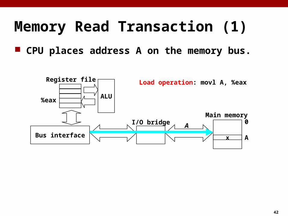
Memory Read Transaction (1) CPU places address A on the memory bus.
ALU
Register file
Bus interface
A0
Ax
Main memoryI/O bridge
%eax
Load operation: movl A, %eax
43
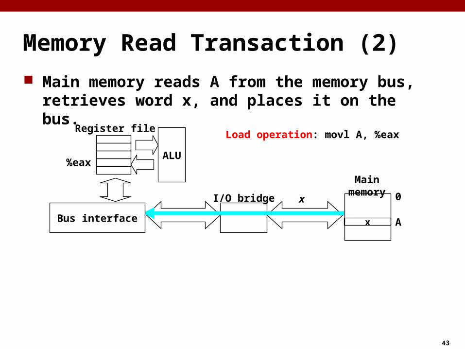
Memory Read Transaction (2) Main memory reads A from the memory bus, retrieves
word x, and places it on the bus.
ALU
Register file
Bus interface
x 0
Ax
Main memory
%eax
I/O bridge
Load operation: movl A, %eax
44
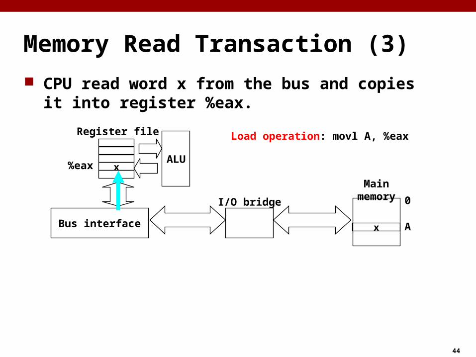
Memory Read Transaction (3) CPU read word x from the bus and copies it into register
%eax.
xALU
Register file
Bus interface x
Main memory0
A
%eax
I/O bridge
Load operation: movl A, %eax
45
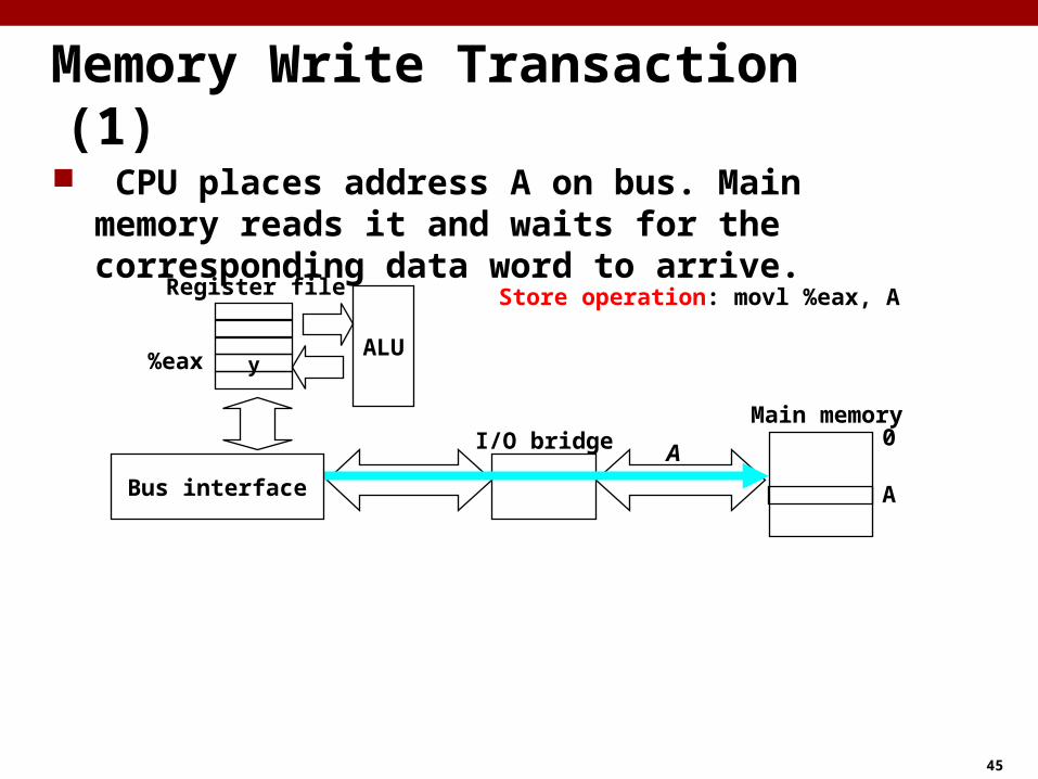
Memory Write Transaction (1) CPU places address A on bus. Main memory reads it and
waits for the corresponding data word to arrive.
yALU
Register file
Bus interface
A
Main memory0
A
%eax
I/O bridge
Store operation: movl %eax, A
46
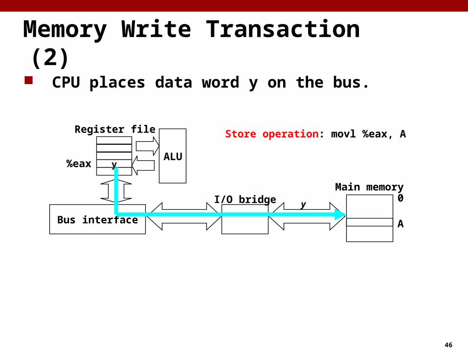
Memory Write Transaction (2) CPU places data word y on the bus.
yALU
Register file
Bus interface
y
Main memory0
A
%eax
I/O bridge
Store operation: movl %eax, A
47
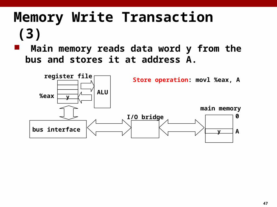
Memory Write Transaction (3) Main memory reads data word y from the bus and stores
it at address A.
yALU
register file
bus interface y
main memory0
A
%eax
I/O bridge
Store operation: movl %eax, A
48
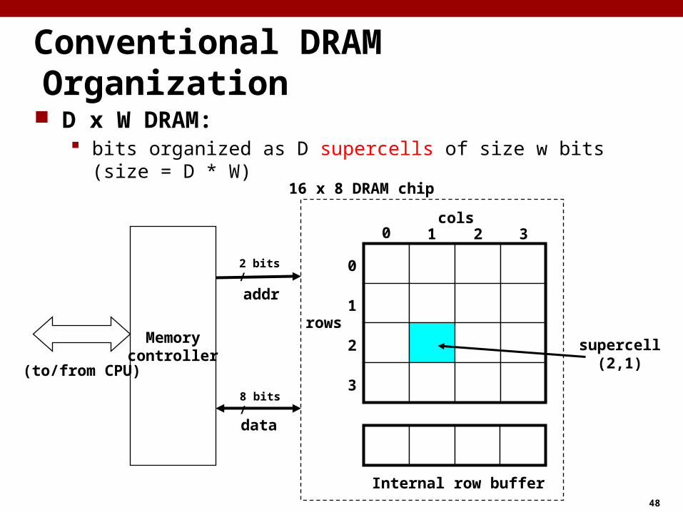
Conventional DRAM Organization D x W DRAM:
bits organized as D supercells of size w bits (size = D * W)
cols
rows
0 1 2 3
0
1
2
3
Internal row buffer
16 x 8 DRAM chip
addr
data
supercell(2,1)
2 bits/
8 bits/
Memorycontroller
(to/from CPU)
49
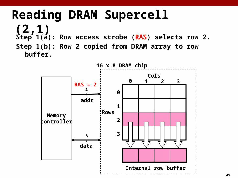
Reading DRAM Supercell (2,1)Step 1(a): Row access strobe (RAS) selects row 2.Step 1(b): Row 2 copied from DRAM array to row buffer.
Cols
Rows
RAS = 20 1 2 3
0
1
2
Internal row buffer
16 x 8 DRAM chip
3
addr
data
2/
8/
Memorycontroller
50
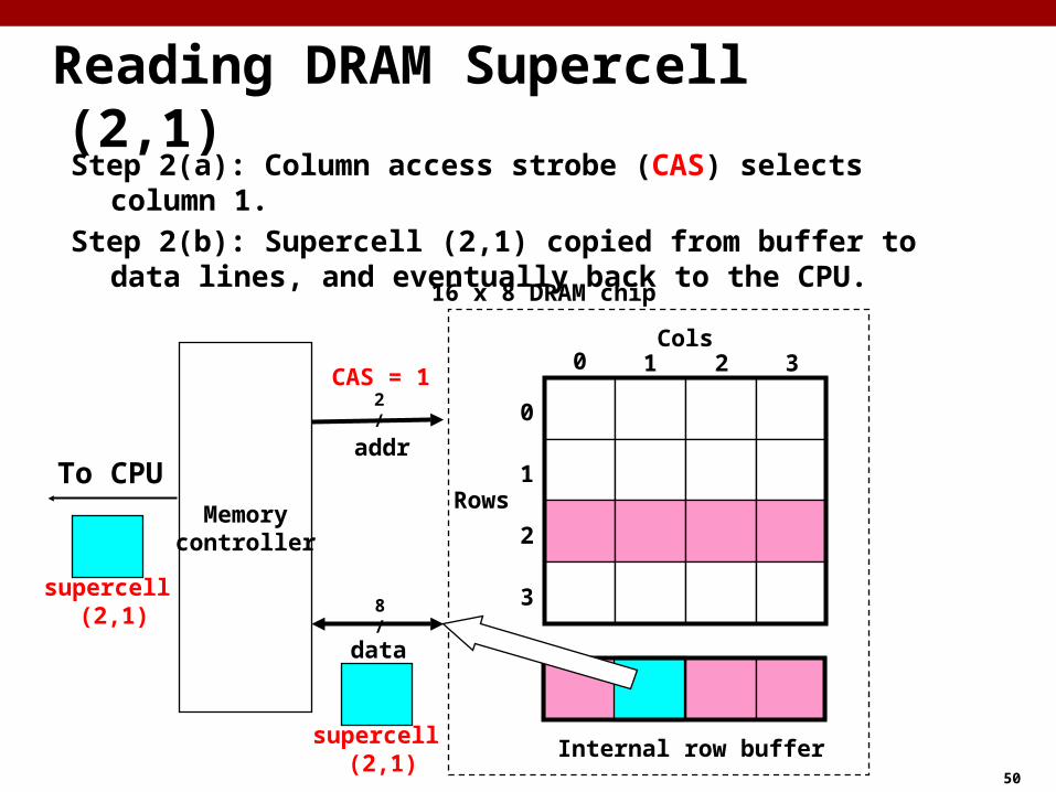
Reading DRAM Supercell (2,1)Step 2(a): Column access strobe (CAS) selects column 1.Step 2(b): Supercell (2,1) copied from buffer to data lines, and eventually
back to the CPU.
Cols
Rows
0 1 2 3
0
1
2
3
Internal row buffer
16 x 8 DRAM chip
CAS = 1
addr
data
2/
8/
Memorycontroller
supercell (2,1)
supercell (2,1)
To CPU
51
Memory Modules
: supercell (i,j)
64 MB memory moduleconsisting ofeight 8Mx8 DRAMs
addr (row = i, col = j)
Memorycontroller
DRAM 7
DRAM 0
031 78151623243263 394047485556
64-bit doubleword at main memory address A
bits0-7
bits8-15
bits16-23
bits24-31
bits32-39
bits40-47
bits48-55
bits56-63
64-bit doubleword
031 78151623243263 394047485556
52
Enhanced DRAMs Basic DRAM cell has not changed since its invention in 1966. DRAM cores with better interface logic and faster I/O :
Synchronous DRAM (SDRAM) Uses a conventional clock signal instead of asynchronous control Allows reuse of the row addresses (e.g., RAS, CAS, CAS, CAS)
Double data-rate synchronous DRAM (DDR SDRAM) Double edge clocking sends two bits per cycle per pin Different types distinguished by size of small prefetch buffer:
– DDR (2 bits), DDR2 (4 bits), DDR4 (8 bits) By 2010, standard for most server and desktop systems Intel Core i7 supports only DDR3 SDRAM

53
Metric 1980 1985 1990 1995 2000 2005 20102010:1980
$/MB 8,000 880 100 30 1 0.1 0.06130,000access (ns) 375 200 100 70 60 50 40 9typical size (MB) 0.064 0.256 4 16 64 2,000 8,000125,000
Storage Trends
DRAM
SRAM
Metric 1980 1985 1990 1995 2000 2005 20102010:1980
$/MB 500 100 8 0.30 0.01 0.005 0.00031,600,000access (ms) 87 75 28 10 8 4 3 29typical size (MB) 1 10 160 1,000 20,000 160,000 1,500,0001,500,000
Disk
Metric 1980 1985 1990 1995 2000 2005 20102010:1980
$/MB 19,200 2,900 320 256 100 75 60 320access (ns) 300 150 35 15 3 2 1.5 200
54
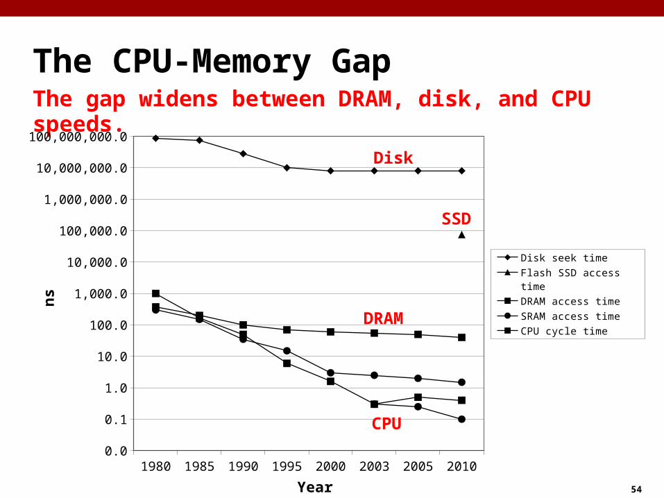
The CPU-Memory GapThe gap widens between DRAM, disk, and CPU speeds.
1980 1985 1990 1995 2000 2003 2005 20100.0
0.1
1.0
10.0
100.0
1,000.0
10,000.0
100,000.0
1,000,000.0
10,000,000.0
100,000,000.0
Disk seek time
Flash SSD access time
DRAM access time
SRAM access time
CPU cycle time
Effective CPU cycle time
Year
ns
Disk
DRAM
CPU
SSD
55
Locality to the Rescue!
The key to bridging this CPU-Memory gap is a fundamental property of computer programs known as locality
56
Topics Storage technologies and trends Locality of reference Caching in the memory hierarchy

57
Locality Principle of Locality: Programs tend to use data and
instructions with addresses near or equal to those they have used recently
Temporal locality: Recently referenced items are likely
to be referenced again in the near future
Spatial locality: Items with nearby addresses tend
to be referenced close together in time
58
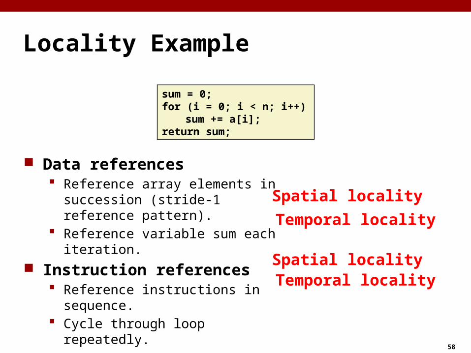
Locality Example
Data references Reference array elements in succession
(stride-1 reference pattern). Reference variable sum each iteration.
Instruction references Reference instructions in sequence. Cycle through loop repeatedly.
sum = 0;for (i = 0; i < n; i++)
sum += a[i];return sum;
Spatial localityTemporal locality
Spatial localityTemporal locality
59
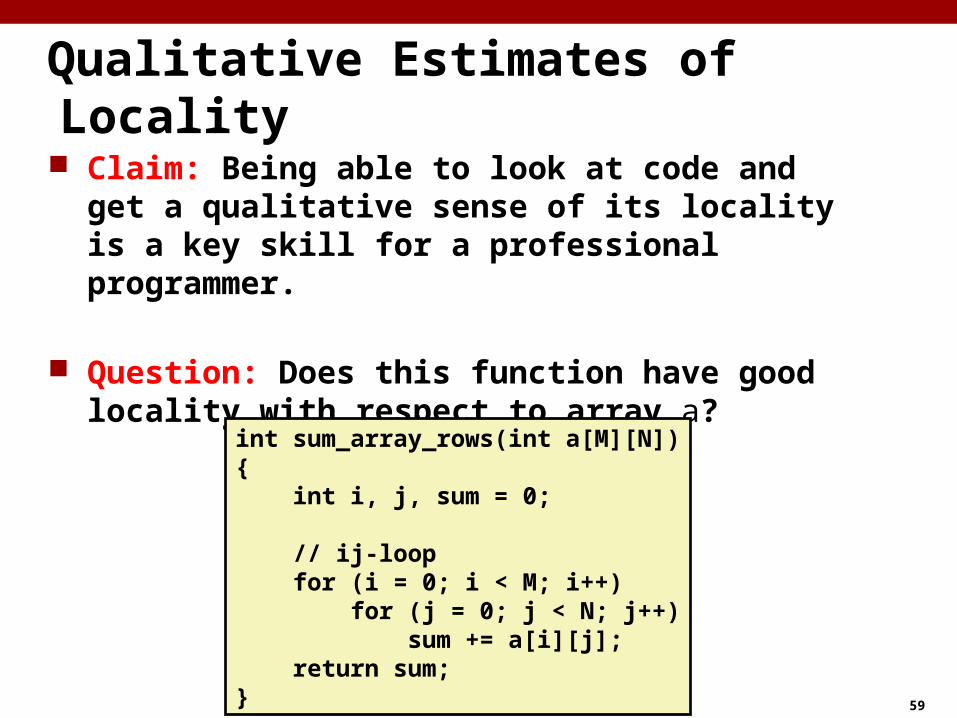
Qualitative Estimates of Locality Claim: Being able to look at code and get a qualitative
sense of its locality is a key skill for a professional programmer.
Question: Does this function have good locality with respect to array a?
int sum_array_rows(int a[M][N]){ int i, j, sum = 0;
// ij-loop for (i = 0; i < M; i++) for (j = 0; j < N; j++) sum += a[i][j]; return sum;}
60
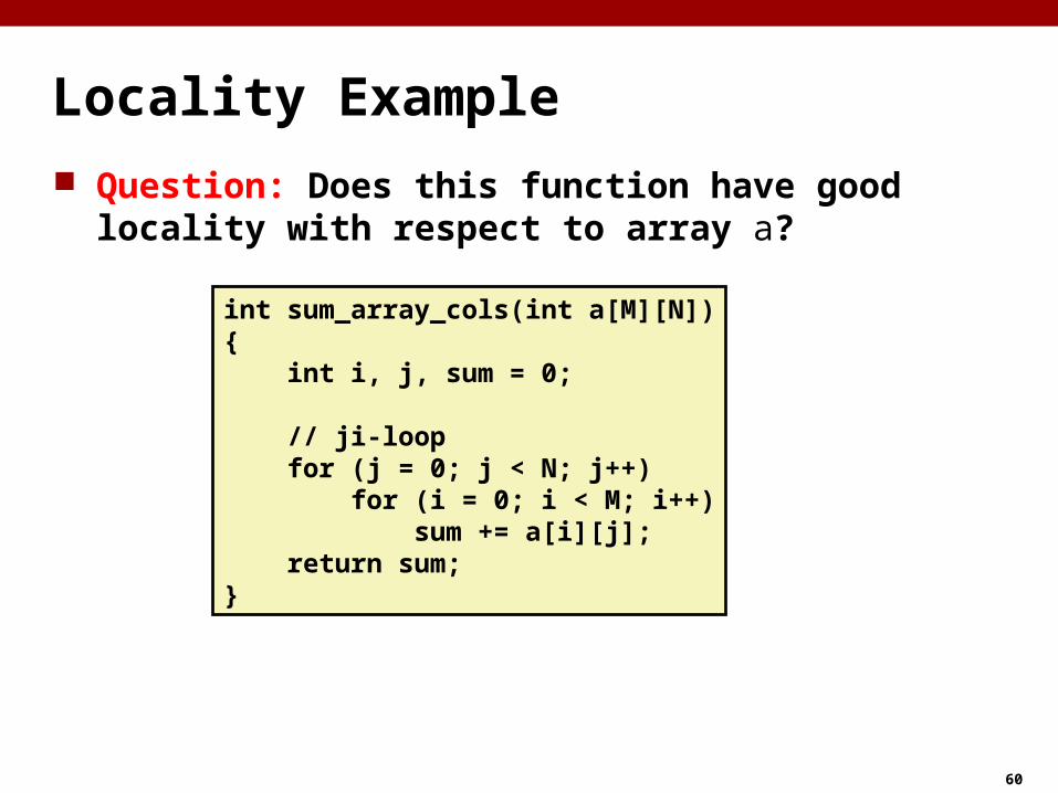
Locality Example Question: Does this function have good locality with
respect to array a?
int sum_array_cols(int a[M][N]){ int i, j, sum = 0;
// ji-loop for (j = 0; j < N; j++) for (i = 0; i < M; i++) sum += a[i][j]; return sum;}

61
Locality Example Question: Can you permute the loops so that the function
scans the 3-d array a with a stride-1 reference pattern (and thus has good spatial locality)?
int sum_array_3d(int a[M][N][N]){ int i, j, k, sum = 0;
for (i = 0; i < M; i++) for (j = 0; j < N; j++) for (k = 0; k < N; k++) sum += a[k][i][j]; return sum;}
62
Memory Hierarchies Some fundamental properties of hardware:
Fast storage technologies cost more per byte, have less capacity, and require more power (heat!).
The gap between CPU and main memory speed is widening.
Solution: organize memory and storage systems in a memory hierarchy.
63
Topics Storage technologies and trends Locality of reference Caching in the memory hierarchy
64
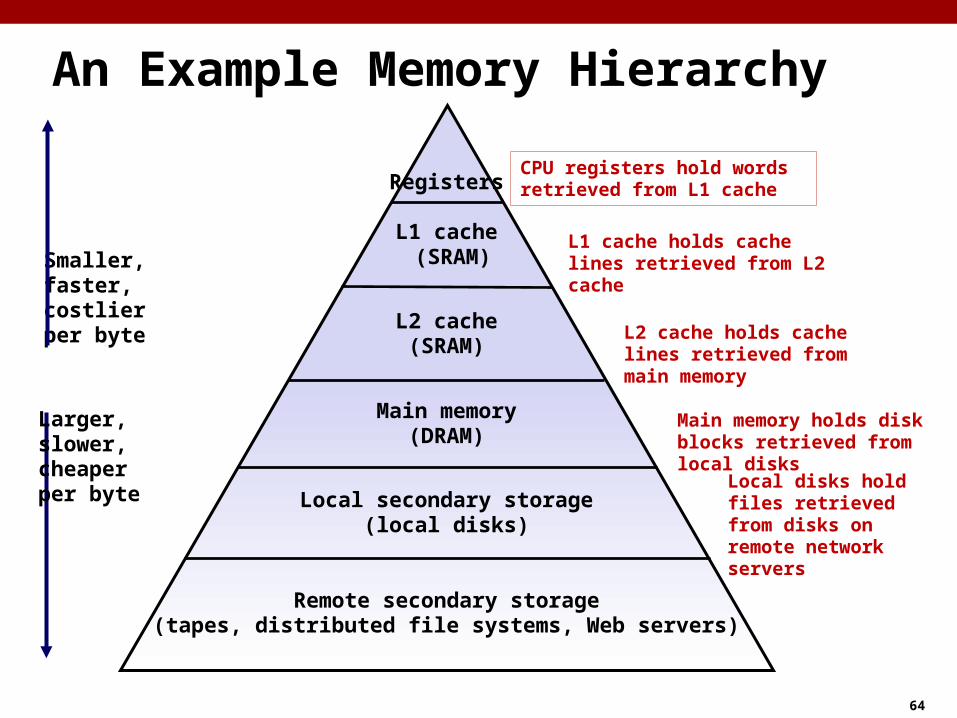
An Example Memory Hierarchy
Registers
L1 cache (SRAM)
Main memory(DRAM)
Local secondary storage(local disks)
Larger, slower, cheaper per byte
Remote secondary storage(tapes, distributed file systems, Web servers)
Local disks hold files retrieved from disks on remote network servers
Main memory holds disk blocks retrieved from local disks
L2 cache(SRAM)
L1 cache holds cache lines retrieved from L2 cache
CPU registers hold words retrieved from L1 cache
L2 cache holds cache lines retrieved from main memory
Smaller,faster,costlierper byte
65
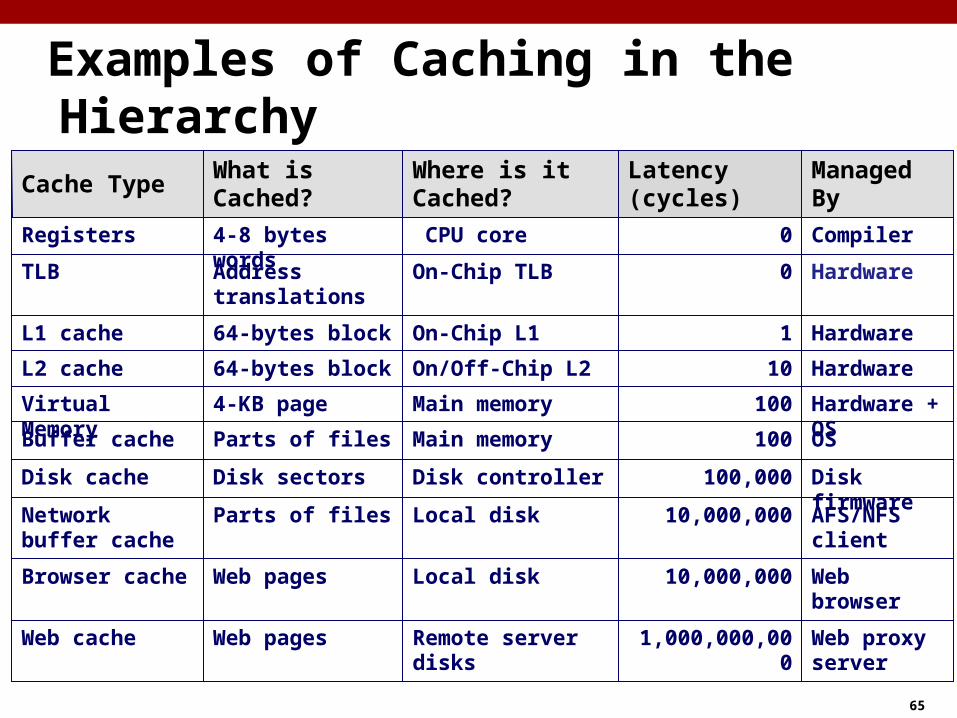
Examples of Caching in the Hierarchy
Hardware0On-Chip TLBAddress translationsTLB
Web browser10,000,000Local diskWeb pagesBrowser cache
Web cache
Network buffer cache
Buffer cache
Virtual Memory
L2 cache
L1 cache
Registers
Cache Type
Web pages
Parts of files
Parts of files
4-KB page
64-bytes block
64-bytes block
4-8 bytes words
What is Cached?
Web proxy server
1,000,000,000Remote server disks
OS100Main memory
Hardware1On-Chip L1
Hardware10On/Off-Chip L2
AFS/NFS client10,000,000Local disk
Hardware + OS100Main memory
Compiler0 CPU core
Managed ByLatency (cycles)Where is it Cached?
Disk cache Disk sectors Disk controller 100,000 Disk firmware

66
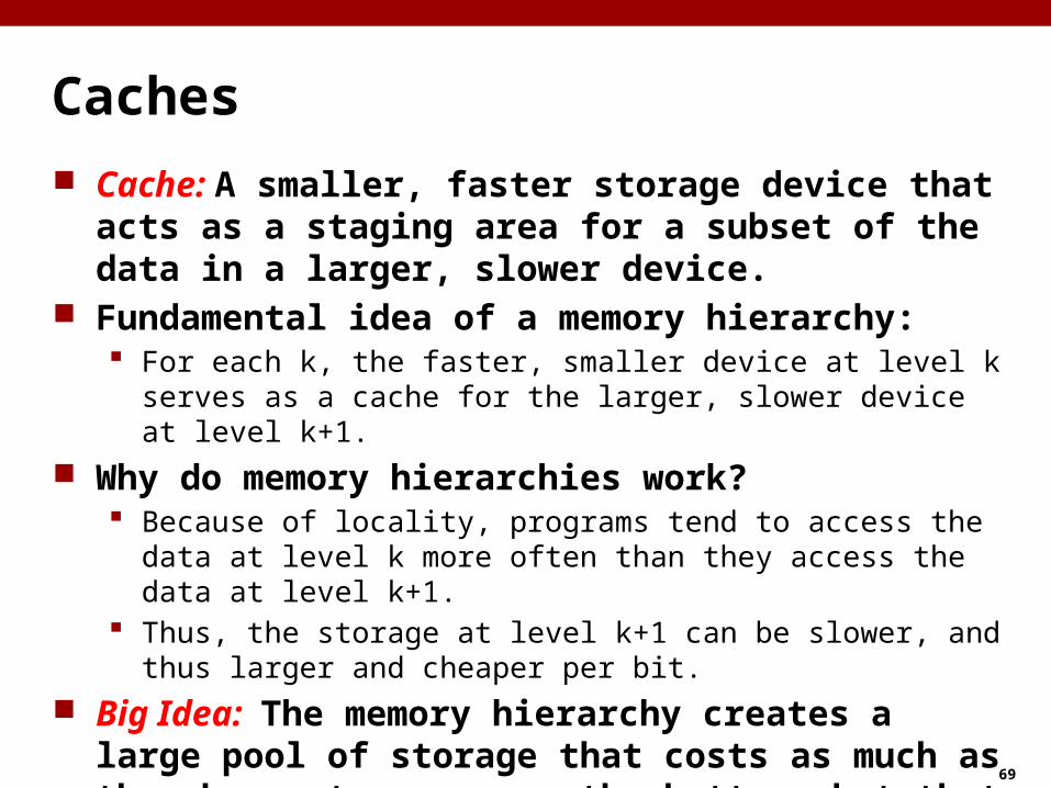
Caches Cache: A smaller, faster storage device that acts as a staging
area for a subset of the data in a larger, slower device.
67
Caches Cache: A smaller, faster storage device that acts as a staging
area for a subset of the data in a larger, slower device. Fundamental idea of a memory hierarchy:
For each k, the faster, smaller device at level k serves as a cache for the larger, slower device at level k+1.
68
Caches Cache: A smaller, faster storage device that acts as a staging
area for a subset of the data in a larger, slower device. Fundamental idea of a memory hierarchy:
For each k, the faster, smaller device at level k serves as a cache for the larger, slower device at level k+1.
Why do memory hierarchies work? Because of locality, programs tend to access the data at level k more
often than they access the data at level k+1. Thus, the storage at level k+1 can be slower, and thus larger and cheaper
per bit.
69
Caches Cache: A smaller, faster storage device that acts as a staging
area for a subset of the data in a larger, slower device. Fundamental idea of a memory hierarchy:
For each k, the faster, smaller device at level k serves as a cache for the larger, slower device at level k+1.
Why do memory hierarchies work? Because of locality, programs tend to access the data at level k more
often than they access the data at level k+1. Thus, the storage at level k+1 can be slower, and thus larger and cheaper
per bit. Big Idea: The memory hierarchy creates a large pool of
storage that costs as much as the cheap storage near the bottom, but that serves data to programs at the rate of the fast storage near the top.
70
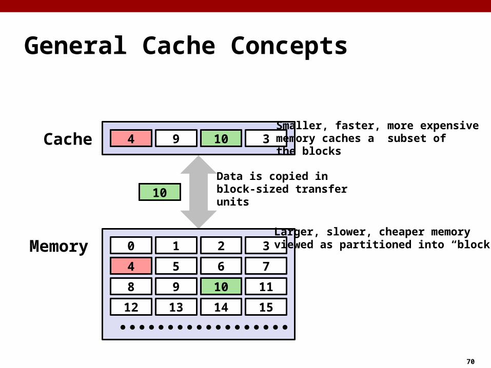
General Cache Concepts
0 1 2 3
4 5 6 7
8 9 10 11
12 13 14 15
8 9 14 3Cache
MemoryLarger, slower, cheaper memoryviewed as partitioned into “blocks”
Data is copied in block-sized transfer units
Smaller, faster, more expensivememory caches a subset ofthe blocks
4
4
4
10
10
10
71
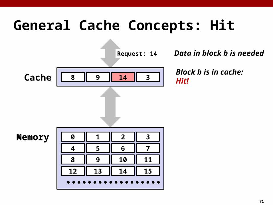
General Cache Concepts: Hit
0 1 2 3
4 5 6 7
8 9 10 11
12 13 14 15
8 9 14 3Cache
Memory
Data in block b is neededRequest: 14
14Block b is in cache:Hit!
72
General Cache Concepts: Miss
0 1 2 3
4 5 6 7
8 9 10 11
12 13 14 15
8 9 14 3Cache
Memory
Data in block b is neededRequest: 12
Block b is not in cache:Miss!
Block b is fetched frommemoryRequest: 12
12
12
12
Block b is stored in cache• Placement policy:
determines where b goes• Replacement policy:
determines which blockgets evicted (victim)
73
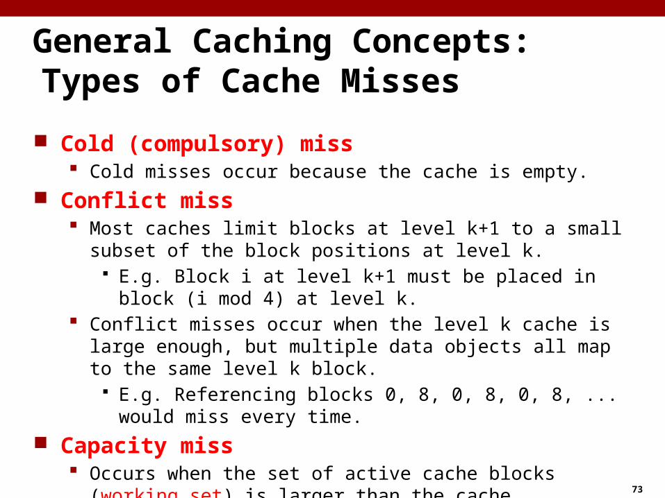
General Caching Concepts: Types of Cache Misses
Cold (compulsory) miss Cold misses occur because the cache is empty.
Conflict miss Most caches limit blocks at level k+1 to a small subset of the block
positions at level k. E.g. Block i at level k+1 must be placed in block (i mod 4) at level k.
Conflict misses occur when the level k cache is large enough, but multiple data objects all map to the same level k block.
E.g. Referencing blocks 0, 8, 0, 8, 0, 8, ... would miss every time. Capacity miss
Occurs when the set of active cache blocks (working set) is larger than the cache.
74
Summary The speed gap between CPU, memory and mass storage
continues to widen.
Well-written programs exhibit a property called locality.
Memory hierarchies based on caching close the gap by exploiting locality.


