disorder-independent control of magnetic monopole defect population in artificial spin-ice...
TRANSCRIPT
Disorder-independent control of magnetic monopole defect population in artificial spin-ice
honeycombs
This article has been downloaded from IOPscience. Please scroll down to see the full text article.
2012 New J. Phys. 14 045010
(http://iopscience.iop.org/1367-2630/14/4/045010)
Download details:
IP Address: 128.143.22.132
The article was downloaded on 09/03/2013 at 14:57
Please note that terms and conditions apply.
View the table of contents for this issue, or go to the journal homepage for more
Home Search Collections Journals About Contact us My IOPscience
T h e o p e n – a c c e s s j o u r n a l f o r p h y s i c s
New Journal of Physics
Disorder-independent control of magnetic monopoledefect population in artificial spin-ice honeycombs
S Ladak1, S K Walton1, K Zeissler1, T Tyliszczak2, D E Read3,W R Branford1,4 and L F Cohen1
1 Blackett Laboratory, Department of Physics, Imperial College,Prince Consort Road, South Kensington, London SW7 2AZ, UK2 Advanced Light Source, Lawrence Berkeley National Laboratory, MS 6-2100,Berkeley, CA 94720, USA3 School of Physics and Astronomy, Cardiff University, The Parade,Cardiff CF24 3AA, UKE-mail: [email protected]
New Journal of Physics 14 (2012) 045010 (12pp)Received 6 December 2011Published 26 April 2012Online at http://www.njp.org/doi:10.1088/1367-2630/14/4/045010
Abstract. Breakdown of the ice rule in artificial spin-ice nanostructures resultsin magnetic monopole defects with zero magnetic moment. Such defects existduring the magnetic switching process in some nanostructures and yet are absentin other apparently similar arrays having the same geometry and made from thesame material components. One explanation proposed for this discrepancy isthat it is due to the variation of disorder across samples, with monopole defectformation occuring only in highly disordered samples. Although disorder canindeed play a role in the determination of monopole density, in this paper weshow, by experiment and simulation, that in samples of similar, low disorder,the factor controlling the nature of magnetic switching is whether the domainwalls are in the transverse wall regime or in the vortex wall regime. Thiswork illustrates that monopole formation can be controlled by intrinsic micro-magnetic behaviour as well as by extrinsic quenched disorder.
4 Author to whom any correspondence should be addressed.
New Journal of Physics 14 (2012) 0450101367-2630/12/045010+12$33.00 © IOP Publishing Ltd and Deutsche Physikalische Gesellschaft
2
Contents
1. Introduction 22. Method 43. Results 44. Discussion 7References 11
1. Introduction
Artificial spin-ice materials [1] are arrays of frustrated nanomagnets and have recently beenshown to be ideal tuneable systems enabling unparalleled studies of frustration. Two differentartificial spin-ice systems have been studied to date and these consist of nanomagnets arrangedin a square [1] and a Kagome lattice [2–5]. The magnetization of each bar is single domain andpoints along the long axis of the bar and thus can be considered an Ising macrospin. Each baris well described as a dumbbell with a magnetic charge of +q at its head and −q at its tail,where q is the magnetization of the bar divided by its length. Within the array this effectivelyquantizes the local magnetic charge at each vertex, Q = 6q, into integers of q. The ice rule inspin ices, in general, can be understood as local magnetic charge minimization. In the Kagomeartificial spin-ice system, three bars meet at each vertex leading naturally to magnetic frustrationwith a finite magnetic charge at each vertex [3]. The ice rule local ordering principle favoursthe set of six possible vertex configurations with Q = ±1q, and suppresses the unique ice-rule-violating configurations known as monopole defects that possess Q = +3q and Q = −3q andzero dipole moment. The ice-rule-obeying configurations occur when one spin points into avertex and two spins point out (1-in, 2-out; Q = −1q) or the opposite (2-in, 1-out; Q = +1q).The nanoarrays we consider here are composed of individual bars of length l = 1500 ± 10 nmand width w = 100 ± 10 nm. These bars are of sufficient dimension and shape anisotropy formagnetic reversal to be mediated by domain wall motion (rather than coherent rotation [6]).Head-to-head domain walls have charge Q = +2q and tail-to-tail domains walls carry chargeQ = −2q.
Recent studies [4, 6–8] have shown that cycling a Kagome artificial spin-ice system throughits hysteresis loop leads to the generation of magnetic monopole defects. However, these defectshave been absent in equivalent switching experiments of nominally similar structures [2]. Whenpreviously we considered connected cobalt [3] honeycombs, we found that the parametersthat enter the problem of creation and imaging of monopole defects can be mapped onto asimple model that requires only the ice-rule violation field (HI) and the distribution (standarddeviation, σ ) of bar coercivities. Our simulated monopole defect population matched theexperimental observation (∼1% of vertices) for σ/HI = 1. The monopole defects observed inthis study were formed in an extrinsic process involving a single domain wall and a change invertex charge of ±2q. A simple, purely Coulombic model treating domain walls as circular discsof magnetic charge with diameter w has subsequently been developed [5, 9, 10], which providesan elegant picture of the physical origin of HI and predicts well the occurrence or absence ofextrinsic monopole defects [5]. Thus in that model the presence [3, 7] or absence [2, 5] ofmonopole defects was attributed solely to the disorder of the system [5].
New Journal of Physics 14 (2012) 045010 (http://www.njp.org/)
3
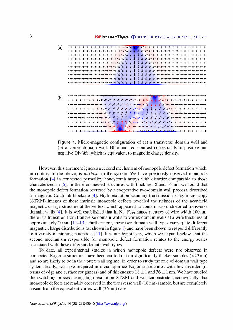
Figure 1. Micro-magnetic configuration of (a) a transverse domain wall and(b) a vortex domain wall. Blue and red contrast corresponds to positive andnegative Div(M), which is equivalent to magnetic charge density.
However, this argument ignores a second mechanism of monopole defect formation which,in contrast to the above, is intrinsic to the system. We have previously observed monopoleformation [4] in connected permalloy honeycomb arrays with disorder comparable to thosecharacterized in [5]. In these connected structures with thickness 8 and 16 nm, we found thatthe monopole defect formation occurred by a cooperative two-domain wall process, describedas magnetic Coulomb blockade [4]. High-resolution scanning transmission x-ray microscopy(STXM) images of these intrinsic monopole defects revealed the richness of the near-fieldmagnetic charge structure at the vertex, which appeared to contain two undistorted transversedomain walls [4]. It is well established that in Ni81Fe19 nanostructures of wire width 100 nm,there is a transition from transverse domain walls to vortex domain walls at a wire thickness ofapproximately 20 nm [11–13]. Furthermore, these two domain wall types carry quite differentmagnetic charge distributions (as shown in figure 1) and have been shown to respond differentlyto a variety of pinning potentials [11]. It is our hypothesis, which we expand below, that thesecond mechanism responsible for monopole defect formation relates to the energy scalesassociated with these different domain wall types.
To date, all experimental studies in which monopole defects were not observed inconnected Kagome structures have been carried out on significantly thicker samples (>23 nm)and so are likely to be in the vortex wall regime. In order to study the role of domain wall typesystematically, we have prepared artificial spin-ice Kagome structures with low disorder (interms of edge and surface roughness) and of thicknesses 18 ± 1 and 36 ± 1 nm. We have studiedthe switching process using high-resolution STXM and we demonstrate unequivocally thatmonopole defects are readily observed in the transverse wall (18 nm) sample, but are completelyabsent from the equivalent vortex wall (36 nm) case.
New Journal of Physics 14 (2012) 045010 (http://www.njp.org/)
4
We use micro-magnetic simulations to investigate the pinning potentials in the transversewall and vortex wall regimes. The striking difference between the two domain wall regimeshighlights the limitations of models which treat the domain walls as simple spheres of magneticcharge [9]. In fact, we also observe strong differences in the cascade behaviour of the walls asthey flow through the lattice. In general, we find that the simple picture of a spherical chargecarrier works well in the vortex regime but, in the transverse regime, locally correlated domainwall processes, such as cascade branching and magnetic Coulomb blockade, play a significantrole.
2. Method
Samples were fabricated by e-beam lithography on SiN membranes, evaporation of Ni81Fe19
and lift-off. The array had a triangular injection pad on the left-hand side in order to studycontrolled domain wall injection. The results of this study will be published elsewhere. Atomicforce microscopy (AFM) was used to measure the sample thickness and surface roughness.Samples were fabricated at thicknesses of 36 ± 1 nm (sample V) and 18 ± 1 nm (sample T), inorder to probe the reversal of systems in the transverse and the vortex domain wall regime,respectively. The rms surface roughness calculated over an area of (100 µm)2 is 2.27 nmfor sample V and 1.12 nm for sample T. Room-temperature STXM studies were carried outon beamline 11.02 at the Advanced Light Source (Berkeley, CA, USA). The sample wasmounted in the STXM chamber between the pole pieces of an electromagnet, which allowedthe application of an in-plane field of ±60 mT in situ. The chamber was pumped downto a pressure of approximately 100 mTorr before filling with He gas. Elliptically polarizedx-rays were provided by an undulating beamline, after which they were focused to a spotsize of approximately 30 nm using a Fresnel zone plate. The sample and electromagnet weremounted at approximately 30◦ with respect to the x-ray propagation vector, enabling the in-plane component of the magnetization to be probed, using the x-ray magnetic circular dichroismeffect. In order to study the switching of the array, the sample was first saturated in the positivefield direction, and small field increments were applied in the negative field direction. Micro-magnetic simulations were performed with the OOMMF [15] package with a lateral mesh sizeof 5 nm. The magnetocrystalline anisotropy of Ni81Fe19 was assumed to be zero, the exchangestiffness was taken to be 1.3 × 10⁻¹¹ J m−1, and the saturation magnetization was taken to be800 emu cm−3.
3. Results
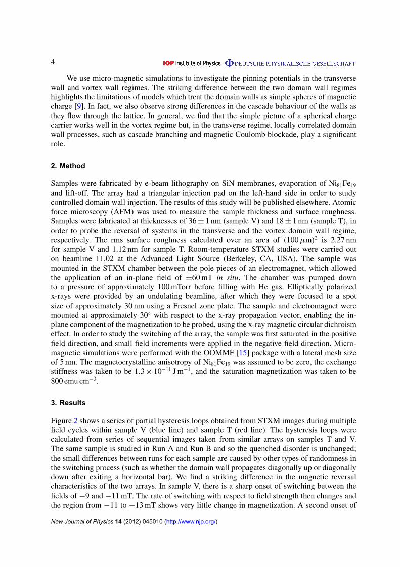
Figure 2 shows a series of partial hysteresis loops obtained from STXM images during multiplefield cycles within sample V (blue line) and sample T (red line). The hysteresis loops werecalculated from series of sequential images taken from similar arrays on samples T and V.The same sample is studied in Run A and Run B and so the quenched disorder is unchanged;the small differences between runs for each sample are caused by other types of randomness inthe switching process (such as whether the domain wall propagates diagonally up or diagonallydown after exiting a horizontal bar). We find a striking difference in the magnetic reversalcharacteristics of the two arrays. In sample V, there is a sharp onset of switching between thefields of −9 and −11 mT. The rate of switching with respect to field strength then changes andthe region from −11 to −13 mT shows very little change in magnetization. A second onset of
New Journal of Physics 14 (2012) 045010 (http://www.njp.org/)
5
-1.0
-0.5
0.0
0.5
1.0
-0.016 -0.014 -0.012 -0.010 -0.008
-1.0
-0.5
0.0
0.5
1.0
M Vortex Run A M Vortex Run BN
orm
aliz
ed M
x
M Transverse Run A M Transverse Run BN
orm
aliz
ed M
x
µ0H (T)
Figure 2. Experimental room-temperature hysteresis loops generated fromSTXM images. Normalized x-component of magnetization versus applied fieldstepped in the −x-direction after saturation in the +x-direction for 36 nm sampleV in the vortex regime (blue circles) and 18 nm sample T in the transverse regime(red squares). The same sample is studied in run A and run B. The error barsare small compared to the symbols and the lines are a guide to the eyes. Theswitching is fundamentally different in the two regimes, yet it is stochastic inboth.
switching occurs at −13 mT and the array is completely switched at −15 mT. Sample T showsvery different characteristics. There is a sharp onset of switching at −12 mT and this continuesunhindered until, at −14 mT, the array is saturated. In order to characterize the distribution ofbar switching fields, in a comparable way to Daunheimer et al [5], the hysteresis loops werefitted to
M(H) =
∑mi erf
(H−H i
c
σi
√2
), (1)
where mi is the amount of magnetic moment that is switched in each event, Hc is the meancoercive field and σi is the standard deviation. In the transverse case, we see only one switchingevent in the loop, and fitting the experimental M(H) curve to equation (1) yields Hc = 12.98 mT,σ = 0.69 mT, which leads to a disorder parameter σ/Hc of 0.049. In the vortex regime there aretwo switching events in the loop and fitting leads to Hc1 = 13.41 mT, σ1 = 1.12 mT, a disorderparameter of 0.084 and Hc2 = 10.25 m, σ2 = 0.86 mT, which also corresponds to a disorderparameter of 0.084. It therefore appears that both samples have a relatively low disorder withσ/Hc < 10%.
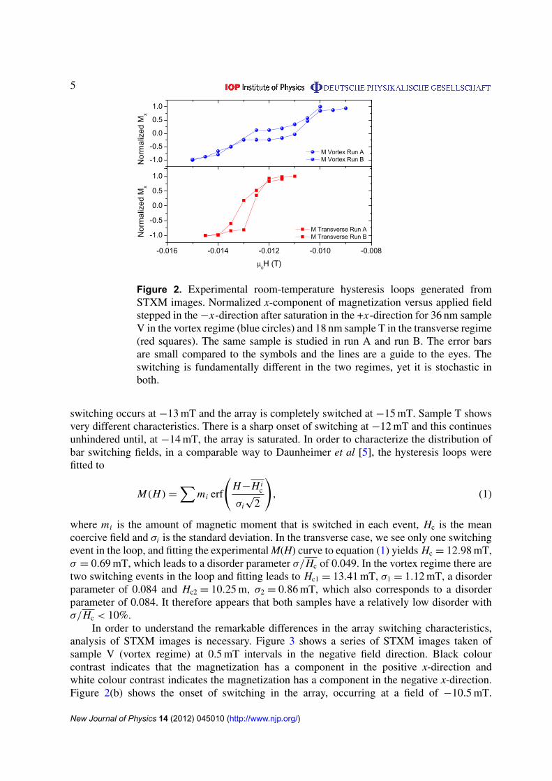
In order to understand the remarkable differences in the array switching characteristics,analysis of STXM images is necessary. Figure 3 shows a series of STXM images taken ofsample V (vortex regime) at 0.5 mT intervals in the negative field direction. Black colourcontrast indicates that the magnetization has a component in the positive x-direction andwhite colour contrast indicates the magnetization has a component in the negative x-direction.Figure 2(b) shows the onset of switching in the array, occurring at a field of −10.5 mT.
New Journal of Physics 14 (2012) 045010 (http://www.njp.org/)
6
Figure 3. Switching of the Kagome artificial spin-ice system in the vortexdomain wall regime under stepwise application of magnetic fields in the−x-direction after saturation in the +x-direction. White contrast indicatespositive x-component of magnetization and black contrast indicates negative Mx .The scale bar represents 10 µm.
Switching starts at the edges of the array and is mediated by domain walls creating long cascadesthat cover the entire length of the array. As the field becomes more negative (figures 3(c)–(f))more cascades are created until the vast majority of the edge bars have switched, leaving isolated
New Journal of Physics 14 (2012) 045010 (http://www.njp.org/)
7
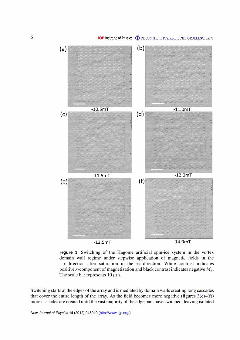
Figure 4. The characteristic ice-rule defect seen at the termination of cascades.White contrast indicates positive x-component of magnetization and blackcontrast indicates negative Mx . The scale bar represents 200 nm.
bars that have not yet switched within the bulk of the array. Further switching within the arrayrequires the nucleation of domain walls from within the bulk of the array, for which there is asubstantial energy cost. In the region from −13 to −15 mT, vortex domain walls are nucleatedin the bulk of the array and the remaining bars within the array switch. Switching within sampleV was studied multiple times, and at no point were monopole defects observed. Where cascadesterminated in an unswitched region, an ice-rule-obeying vertex of opposite magnetic charge isobserved, as shown in figure 4.
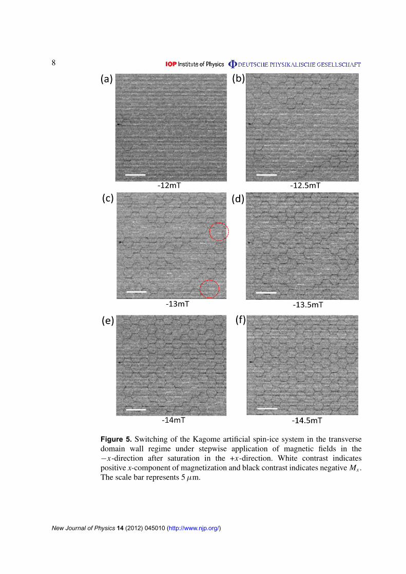
Figure 5 shows some example STXM images taken of sample T (transverse regime) at0.5 mT intervals in the negative field direction. Switching in the transverse regime also startsat the edges of the array. However, the single-chain cascade behaviour observed in the vortexregime does not occur and multiple branches appear quickly in the reversal process. This canalso be seen in the partial hysteresis loop shown in figure 2. Switching takes place rapidlywithin a 2 mT window. The last few bars to switch are those in which the opposite direction ofmagnetization was stabilized by a magnetic Coulomb blockade effect [4] at a monopole defect.Monopole defects are seen during the switching process of sample T, as shown by red circles infigure 5(c), but are relatively rare and occur on less than 1% of the vertices.
4. Discussion
A simple model in which the domain walls are considered to be magnetically charged circulardiscs of diameter w explains well the occurrence of extrinsic monopole defect formation [9]. Themodel results suggest that switching from a Q = +1q to Q = −1q vertex requires the emissionof a Q = +2q DW, so the coercive field can be approximated as the field required to overcomethe Coulombic attraction between the wall and the oppositely charged vertex at the separationw. If all vertices are considered to be structurally identical, then any applied field that causesthis depinning of the wall from the vertex is then also sufficient to push the domain wall towithin a distance w of an oppositely charged vertex and more than enough to depin it from that
New Journal of Physics 14 (2012) 045010 (http://www.njp.org/)
8
Figure 5. Switching of the Kagome artificial spin-ice system in the transversedomain wall regime under stepwise application of magnetic fields in the−x-direction after saturation in the +x-direction. White contrast indicatespositive x-component of magnetization and black contrast indicates negative Mx .The scale bar represents 5 µm.
New Journal of Physics 14 (2012) 045010 (http://www.njp.org/)

9
like-charged vertex. Therefore, the Q = +3 state formed by this process is not a stableintermediate in the switching of a perfect array. Thus, two regimes can be defined by the relativemagnitude of the quenched disorder in the distribution of bar coercivities within the array. Onlyin the strong disorder case, in which the total spread of coercive fields of bars within the arrayis greater than the fields associated with magnetic charge considerations, can monopole defectsreadily form by this extrinsic process.
Our STXM images indicate fundamental differences in the switching processes of anartificial Kagome spin-ice in the transverse and vortex domain wall regimes. Micro-magneticsimulations were performed in order to investigate the difference between intra-array domainwall nucleation fields for transverse and vortex domain walls. In our previous study, we foundthat there was a large disparity (approximately a factor of six) between measured room-temperature switching fields and zero-temperature simulations, which is simply a functionof temperature, and that the simulations gave excellent agreement with images of the localmagnetic structure with a simple linear scaling of the applied field [4]. Zero-temperaturesimulations were performed upon a single vertex, in which a domain wall was placed closeto the vertex centre, on the end of the horizontal bar (oriented in the same direction as theapplied field). A field was then applied to push the domain wall through the vertex and switchthe structure. We find that switching occurs in two distinct stages. At the first stage, the domainwall was pushed into the vertex, resulting in the switching of one of the diagonal bars (Hd).In the second stage, a domain wall actually has to nucleate close to the vertex to switch theremaining diagonal bar (Hn). We found that in the transverse regime, Hd was equal to 29.5 mTand Hn was equal to 56.5 mT, whereas in the vortex regime Hd was equal to 33.0 mT and Hn
was equal to 84.5 mT. When a domain wall reaches a vertex it is presented with a choice of twoequivalent paths; in the vortex wall regime the domain wall acts as a single conserved magneticcharge carrier and selects one path; there is then a large barrier to the switching of the remainingbar, which must switch by propagation of a second domain wall of opposite charge or by intra-array domain wall nucleation. In figure 3(c) at 11 mT all the available edge nucleation pointsin sample V have switched, and each has produced a chain of switched bars right across thesample. A large number of bars (some in quite large domains) have been missed by the edge-nucleated walls, and so switching there can only begin by intra-array domain wall nucleation athigher fields, which can be identified as a clear step in the measured hysteresis loop. As thereis one nucleation point per edge hexagon and the domain wall is choosing one path of two,approximately half of the bars in the array are switched by the edge-nucleated domain wall andthe observed plateau in the MH curve is close to zero magnetization.
In the transverse regime the micro-magnetic simulations indicate that the transit of thedomain wall through the vertex apparently reduces the energy barrier to nucleation of a seconddomain wall at that vertex, causing a branch in the cascade of switched bars from the originaledge nucleation site. This effective amplification of the number of edge-nucleated domain wallsgives a measurable difference to the hysteresis loop structure because the edge nucleation canassist the switching of all of the bars. The only pinning mechanism effective at fields slightlyabove the mean coercive field from edge-nucleated domain walls is the formation of monopoledefects, which are stabilized by a magnetic Coulomb blockade effect between two walls [4].
The other clear difference between the two samples is that monopole defects are readilyobserved in the 18 nm sample (T) in the transverse wall regime, and are not observed in the36 nm sample (V), which is in the vortex wall regime. Monopole defect formation is at leastsomewhat statistical in nature and always comparatively rare, so the data presented here are not
New Journal of Physics 14 (2012) 045010 (http://www.njp.org/)
10
statistically sufficient to claim that monopole defects can never occur. However, given the strongsimilarity of the MH loop of the 36 nm sample in figure 2 to that of Daunheimer et al [5], wheremany more extensive studies have shown that monopole defects are convincingly absent, it isvery likely that we are in the same regime, and the absence of monopole defects is not merelychance. Note that if we attribute the presence of monopoles to high disorder, and parameterizethe two samples with the disorder parameter, σ/Hc, we would obtain disorder parameters of0.049 for T and 0.085 for V and then our predicted monopole populations would not match theexperiment. In fact, the samples were fabricated in parallel processes and the only evidence ofany difference at all in the extrinsic disorder is the greater surface roughness in sample V, whichcannot account for either the unusual shape of the hysteresis loop of sample V or the observationof monopole defects only in sample T. This illustrates that this parameterization method can giveartificially high estimates of the extrinsic disorder for 180◦ reversals [5]. It is our hypothesis thatthe presence or absence of monopole defects is instead controlled by the stability of the magneticCoulomb blockade between two domain walls in close proximity [4]. We have previously shownthat a modified version of the simple Coulombic argument which takes into account the verydifferent transverse domain wall magnetic charge distribution (figure 1) can explain the stabilityof the Coulomb blockade vertex between two transverse walls understanding the analogousprocess in the vortex regime requires some knowledge of the pinning potential at the vertex forvortex domain walls and the magnetic charge distribution of vortex domain walls of differentchirality. In order to determine the pinning potential at the vertex, micro-magnetic simulationswere performed upon a single vertex that had been preset to a Coulomb blockade-type monopoledefect state where it is the bar parallel to the field direction that is unswitched. A field was thenapplied in the positive x-direction in order to determine the field needed to depin a domain walland propagate through the vertex. For transverse domain walls (t = 18 nm) the depinning fieldhere is greater than Hd for the ice-rule vertex, whereas for vortex domain walls (t = 36 nm)the monopole depinning field is less than that of the ice-rule vertex. Thus the simple chargeargument for no monopole defects of Mellado et al [9] works well in the vortex case. Thisobservation is unsurprising as the magnetic charge distribution in a vortex domain wall is muchcloser to the charged circular disc approximation.
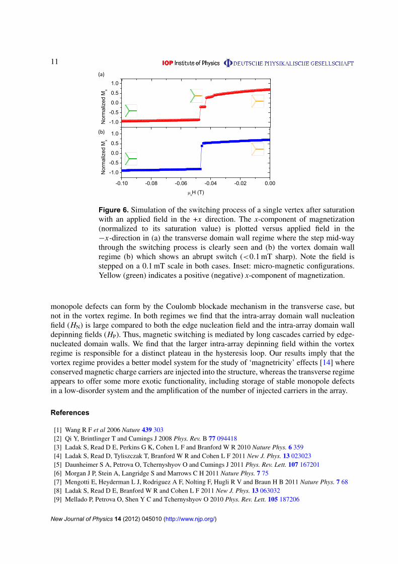
The enhanced tendency for monopole defect formation is also illustrated by micro-magnetic simulations of 180◦ reversal in a single vertex. The structures were first saturatedin the positive field direction, after which 0.1 mT steps were applied in the negative fielddirection. This was carried out on samples of 18 and 36 nm thickness. Figure 6 shows thehysteresis loops generated for samples of 18 nm thickness (a) and samples of 36 nm thickness(b) with micro-magnetic configurations (inset). Switching in the 18 nm vertex leads to thecreation of a monopole defect, stabilized by the magnetic Coulomb interaction, as we haveseen previously [4]. This gives a noticeable step in the loop, since a finite amount of field isneeded to overcome the mutual magnetic Coulomb repulsion of the two transverse walls. Thesimulation in the 36 nm structure led to an abrupt switching, and no monopole defect was seen.
In conclusion, we have carried out an extensive study of the magnetic reversal processin the transverse and the vortex domain wall regime for an artificial Kagome spin-ice system.Monopole defects are absent from the reversal in the vortex domain wall regime and this seemsto be due to the difference in magnetic charge configurations of the two wall types. The highlyasymmetric magnetic charge distribution in the transverse walls gives a much stronger inter-wall Coulomb repulsion than in the vortex walls, in which the charge is more diffuse. Hence,
New Journal of Physics 14 (2012) 045010 (http://www.njp.org/)
11
-1.0
-0.5
0.0
0.5
1.0
-0.10 -0.08 -0.06 -0.04 -0.02 0.00
-1.0
-0.5
0.0
0.5
1.0
Nor
mal
ized
Mx
Nor
mal
ized
Mx
H (T)
Figure 6. Simulation of the switching process of a single vertex after saturationwith an applied field in the +x direction. The x-component of magnetization(normalized to its saturation value) is plotted versus applied field in the−x-direction in (a) the transverse domain wall regime where the step mid-waythrough the switching process is clearly seen and (b) the vortex domain wallregime (b) which shows an abrupt switch (<0.1 mT sharp). Note the field isstepped on a 0.1 mT scale in both cases. Inset: micro-magnetic configurations.Yellow (green) indicates a positive (negative) x-component of magnetization.
monopole defects can form by the Coulomb blockade mechanism in the transverse case, butnot in the vortex regime. In both regimes we find that the intra-array domain wall nucleationfield (HN) is large compared to both the edge nucleation field and the intra-array domain walldepinning fields (HP). Thus, magnetic switching is mediated by long cascades carried by edge-nucleated domain walls. We find that the larger intra-array depinning field within the vortexregime is responsible for a distinct plateau in the hysteresis loop. Our results imply that thevortex regime provides a better model system for the study of ‘magnetricity’ effects [14] whereconserved magnetic charge carriers are injected into the structure, whereas the transverse regimeappears to offer some more exotic functionality, including storage of stable monopole defectsin a low-disorder system and the amplification of the number of injected carriers in the array.
References
[1] Wang R F et al 2006 Nature 439 303[2] Qi Y, Brintlinger T and Cumings J 2008 Phys. Rev. B 77 094418[3] Ladak S, Read D E, Perkins G K, Cohen L F and Branford W R 2010 Nature Phys. 6 359[4] Ladak S, Read D, Tyliszczak T, Branford W R and Cohen L F 2011 New J. Phys. 13 023023[5] Daunheimer S A, Petrova O, Tchernyshyov O and Cumings J 2011 Phys. Rev. Lett. 107 167201[6] Morgan J P, Stein A, Langridge S and Marrows C H 2011 Nature Phys. 7 75[7] Mengotti E, Heyderman L J, Rodriguez A F, Nolting F, Hugli R V and Braun H B 2011 Nature Phys. 7 68[8] Ladak S, Read D E, Branford W R and Cohen L F 2011 New J. Phys. 13 063032[9] Mellado P, Petrova O, Shen Y C and Tchernyshyov O 2010 Phys. Rev. Lett. 105 187206
New Journal of Physics 14 (2012) 045010 (http://www.njp.org/)
12
[10] Tchernyshyov O 2010 Nature Phys. 6 323[11] Klaui M 2008 J. Phys.: Condens. Matter 20 313001[12] McMichael R D and Donahue M J 1997 IEEE Trans. Magn. 33 4167[13] Nakatani Y, Thiaville A and Miltat J 2005 J. Magn. Magn. Mater. 290 750[14] Bramwell S T, Giblin S R, Calder S, Aldus R, Prabhakaran D and Fennell T 2009 Nature 461 956[15] The object oriented micromagnetic framework (OOMMF) project at ITL/NIST http://math.nist.gov/oommf
New Journal of Physics 14 (2012) 045010 (http://www.njp.org/)