digital signal processing vlsi...
TRANSCRIPT
1
AMBAAMBA
Ref: AMBA Specification Rev. 2.0
Shao-Yi Chien 2SoC Design Lab
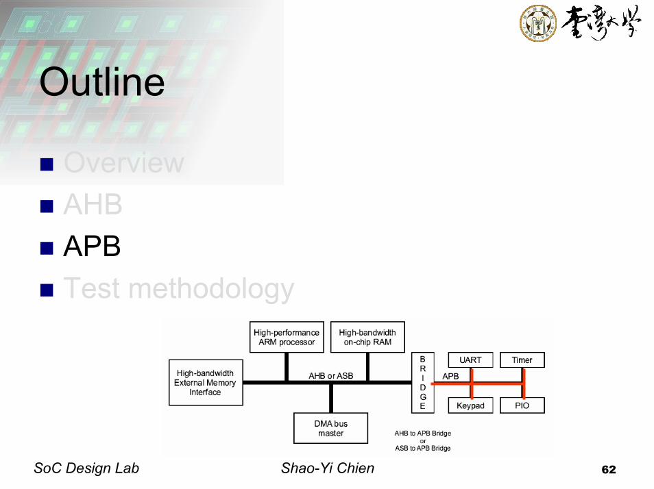
Outline
OverviewAHBAPBTest methodology
Shao-Yi Chien 3SoC Design Lab
Outline
OverviewAHBAPBTest methodology
Shao-Yi Chien 4SoC Design Lab
BUS Brief
In a system, various subsystems must have interfaces to one anotherThe bus serves as a shared communication link between subsystemsAdvantages
Low costVersatility
DisadvantagePerformance bottleneck
Shao-Yi Chien 5SoC Design Lab
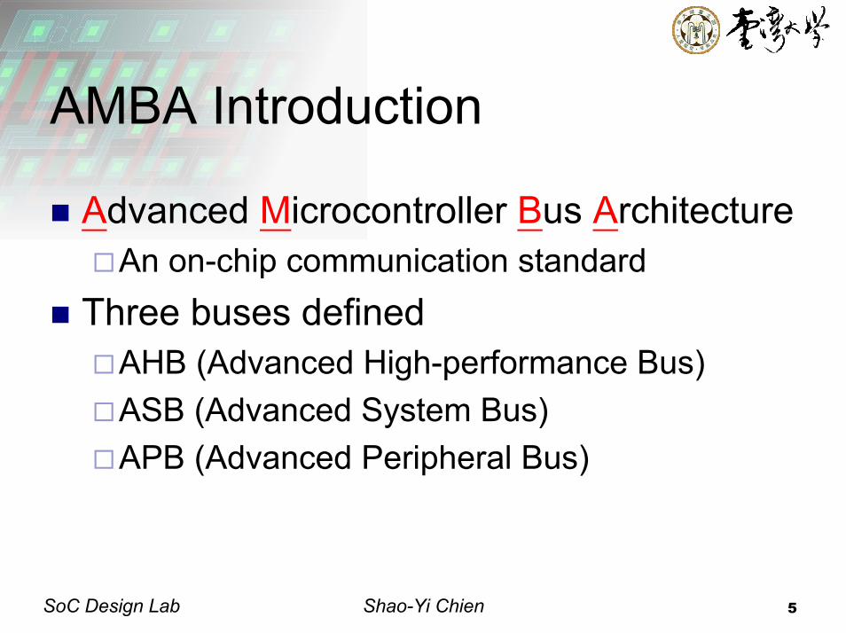
AMBA Introduction
Advanced Microcontroller Bus ArchitectureAn on-chip communication standard
Three buses definedAHB (Advanced High-performance Bus)ASB (Advanced System Bus)APB (Advanced Peripheral Bus)
Shao-Yi Chien 6SoC Design Lab
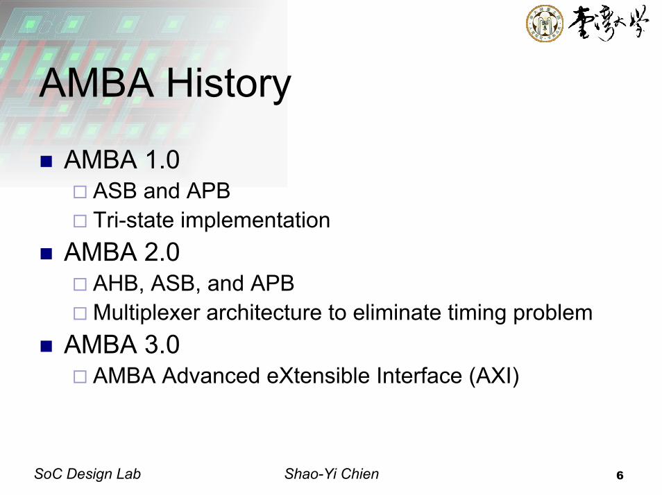
AMBA History
AMBA 1.0ASB and APBTri-state implementation
AMBA 2.0AHB, ASB, and APBMultiplexer architecture to eliminate timing problem
AMBA 3.0AMBA Advanced eXtensible Interface (AXI)
Shao-Yi Chien 7SoC Design Lab
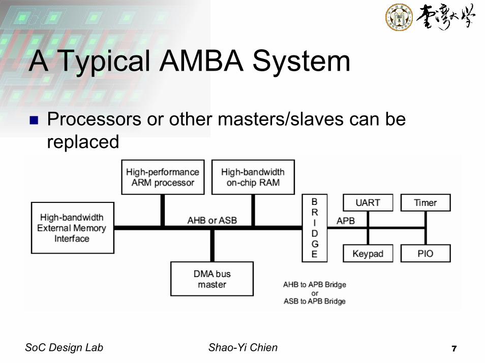
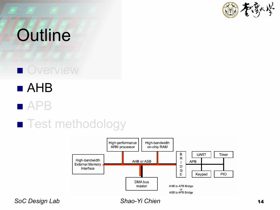
A Typical AMBA System
Processors or other masters/slaves can be replaced
Shao-Yi Chien 8SoC Design Lab
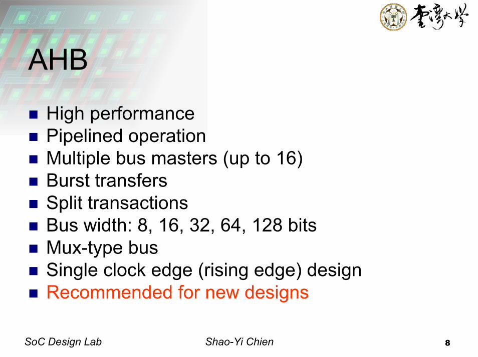
AHB
High performancePipelined operationMultiple bus masters (up to 16)Burst transfersSplit transactionsBus width: 8, 16, 32, 64, 128 bitsMux-type busSingle clock edge (rising edge) designRecommended for new designs
Shao-Yi Chien 9SoC Design Lab
ASB
High performancePipelined operationMultiple bus mastersBurst transfersBus width: 8, 16, 32 bitsTristate-type busFalling edge design
Shao-Yi Chien 10SoC Design Lab
APB
Lower powerLatched address and controlSimple interfaceSuitable for many peripheralsSingle clock edge (rising edge) designAppears as a local secondary bus that is encapsulated as a single AHB or ASB slave devices
Shao-Yi Chien 11SoC Design Lab
AHB ComponentsAHB master
Initiate a read/write operationOnly one master is allowed to use the busuP, DMA, DSP, …
AHB slaveRespond to a read/write operationAddress mappingExternal memory I/F, APB bridge, internal memory, …
AHB arbiterEnsure that which master is activeArbitration algorithm is not defined in ABMA spec.
AHB decoderDecode the address and generate select signal to slaves
Shao-Yi Chien 12SoC Design Lab
APB Components
AHB2APB BridgeProvides latching of all address, data, and control signalsProvides a second level of decoding to generate slave select signals for the APB peripherals
All other modules on the APB are APB slavesUn-pipelinedZero-power interfaceTiming can be provided by decode with strobe timingWrite data valid for the whole acess
Shao-Yi Chien 13SoC Design Lab
Notes on the AMBA Specification
Technology independentNot define electrical characteristicsTiming specification only at the cycle level
Exact timing requirements will depend on the process technology used and operation frequency
Shao-Yi Chien 14SoC Design Lab
Outline
OverviewAHBAPBTest methodology
Shao-Yi Chien 15SoC Design Lab
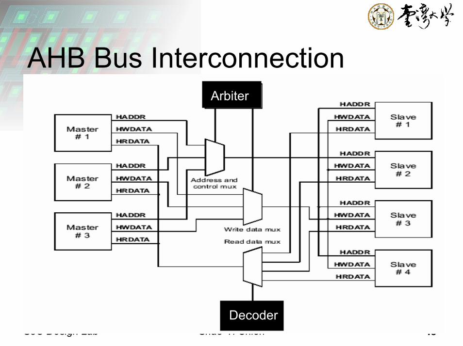
AHB Bus InterconnectionArbiter
Decoder
Shao-Yi Chien 16SoC Design Lab
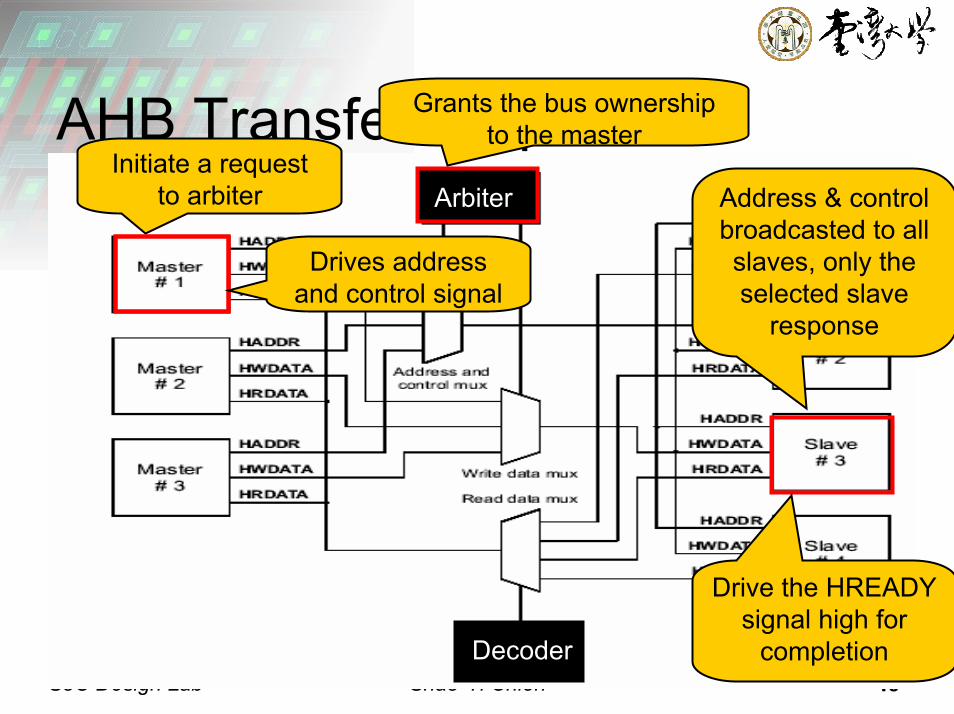
AHB Transfer SequenceArbiter
Decoder
Initiate a request to arbiter
Grants the bus ownership to the master
Drives address and control signal
Address & control broadcasted to all slaves, only the selected slave
response
Drive the HREADY signal high for
completion
Shao-Yi Chien 17SoC Design Lab
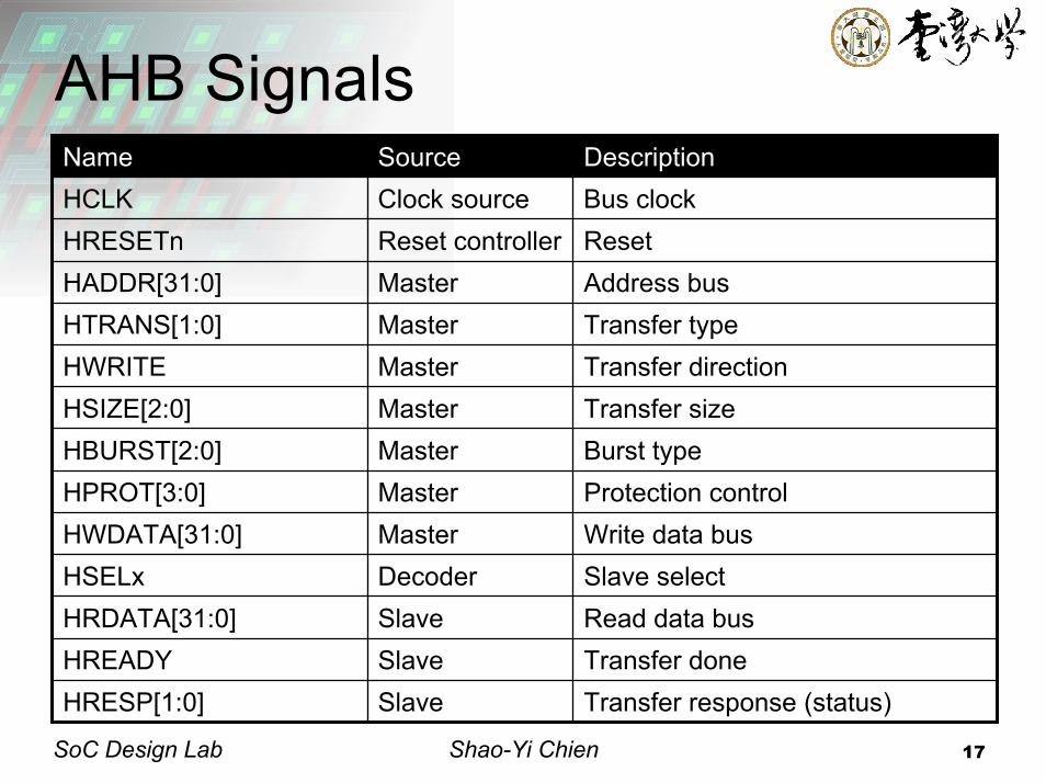
AHB SignalsName Source DescriptionHCLK Clock source Bus clockHRESETn Reset controller ResetHADDR[31:0] Master Address busHTRANS[1:0] Master Transfer typeHWRITE Master Transfer directionHSIZE[2:0] Master Transfer sizeHBURST[2:0] Master Burst typeHPROT[3:0] Master Protection controlHWDATA[31:0] Master Write data busHSELx Decoder Slave selectHRDATA[31:0] Slave Read data busHREADY Slave Transfer doneHRESP[1:0] Slave Transfer response (status)
Shao-Yi Chien 18SoC Design Lab
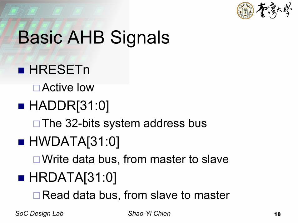
Basic AHB Signals
HRESETnActive low
HADDR[31:0]The 32-bits system address bus
HWDATA[31:0]Write data bus, from master to slave
HRDATA[31:0]Read data bus, from slave to master
Shao-Yi Chien 19SoC Design Lab
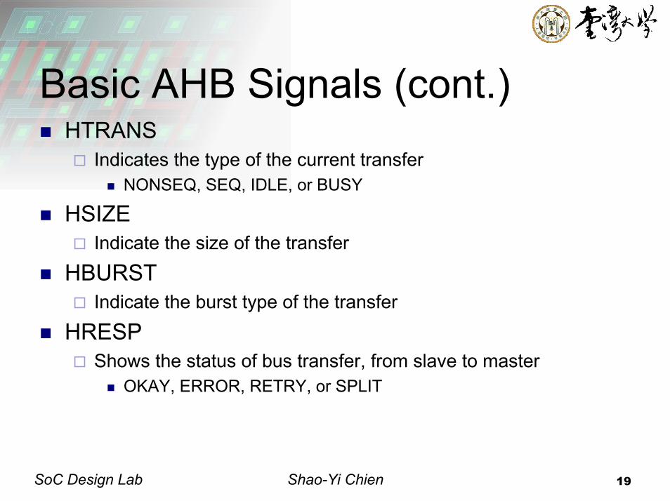
Basic AHB Signals (cont.)HTRANS
Indicates the type of the current transferNONSEQ, SEQ, IDLE, or BUSY
HSIZEIndicate the size of the transfer
HBURSTIndicate the burst type of the transfer
HRESPShows the status of bus transfer, from slave to master
OKAY, ERROR, RETRY, or SPLIT
Shao-Yi Chien 20SoC Design Lab
Basic AHB Signals (cont.)
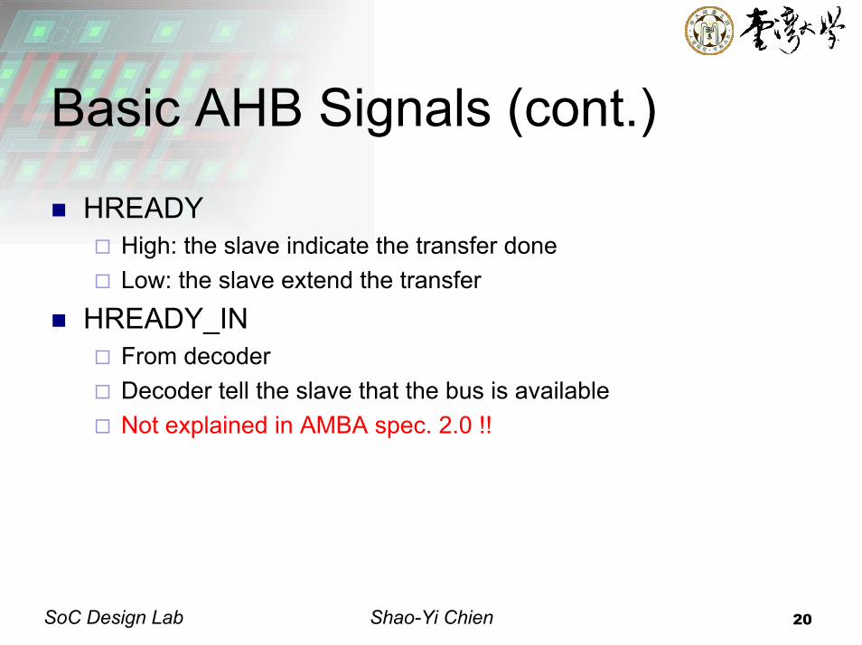
HREADYHigh: the slave indicate the transfer doneLow: the slave extend the transfer
HREADY_INFrom decoderDecoder tell the slave that the bus is availableNot explained in AMBA spec. 2.0 !!
Shao-Yi Chien 21SoC Design Lab
Basic AHB Transfers
Two distinct sectionsThe address phase, only one cycleThe data phase, may required several cycles, achieved by HREADY signals
Pipeline transactionAddress phase is before the data phase
Shao-Yi Chien 22SoC Design Lab
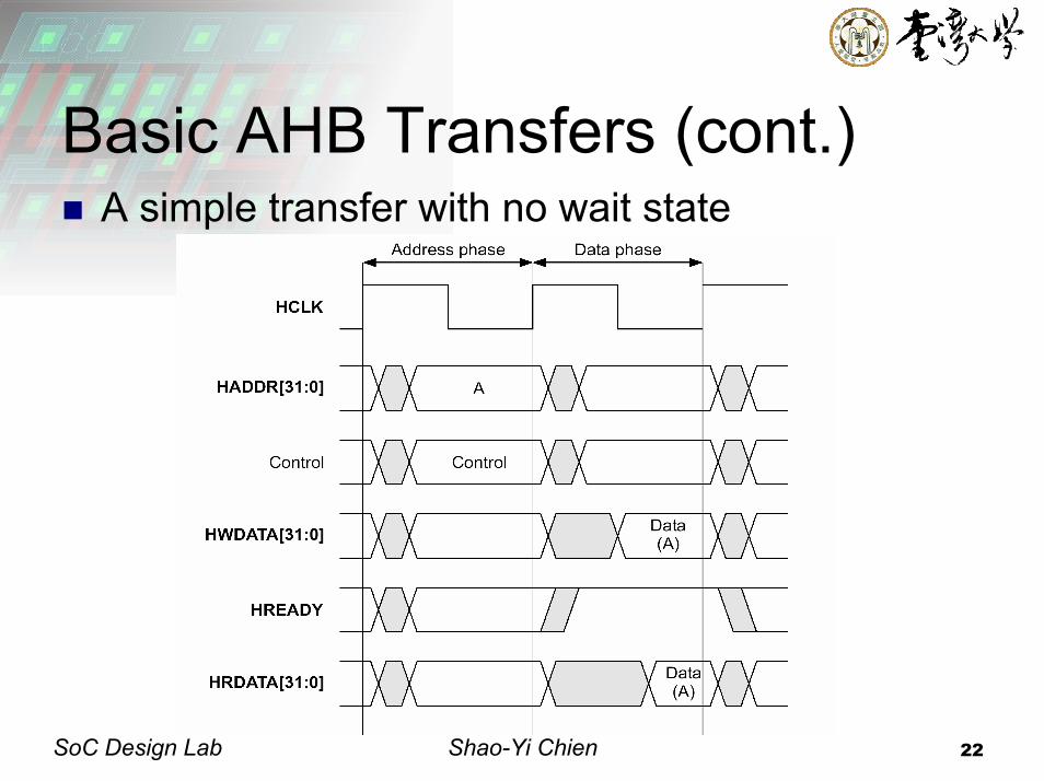
Basic AHB Transfers (cont.)A simple transfer with no wait state
Shao-Yi Chien 23SoC Design Lab
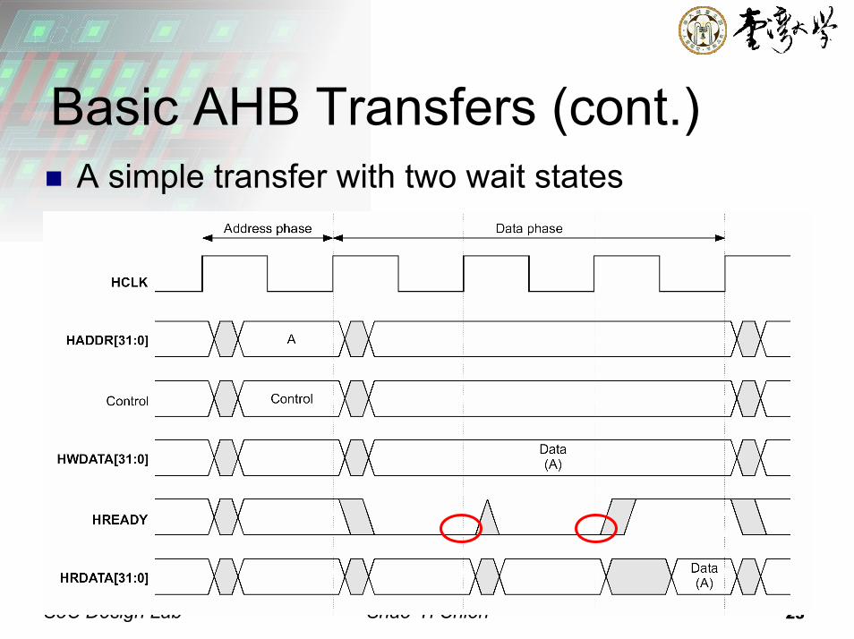
Basic AHB Transfers (cont.)A simple transfer with two wait states
Shao-Yi Chien 24SoC Design Lab
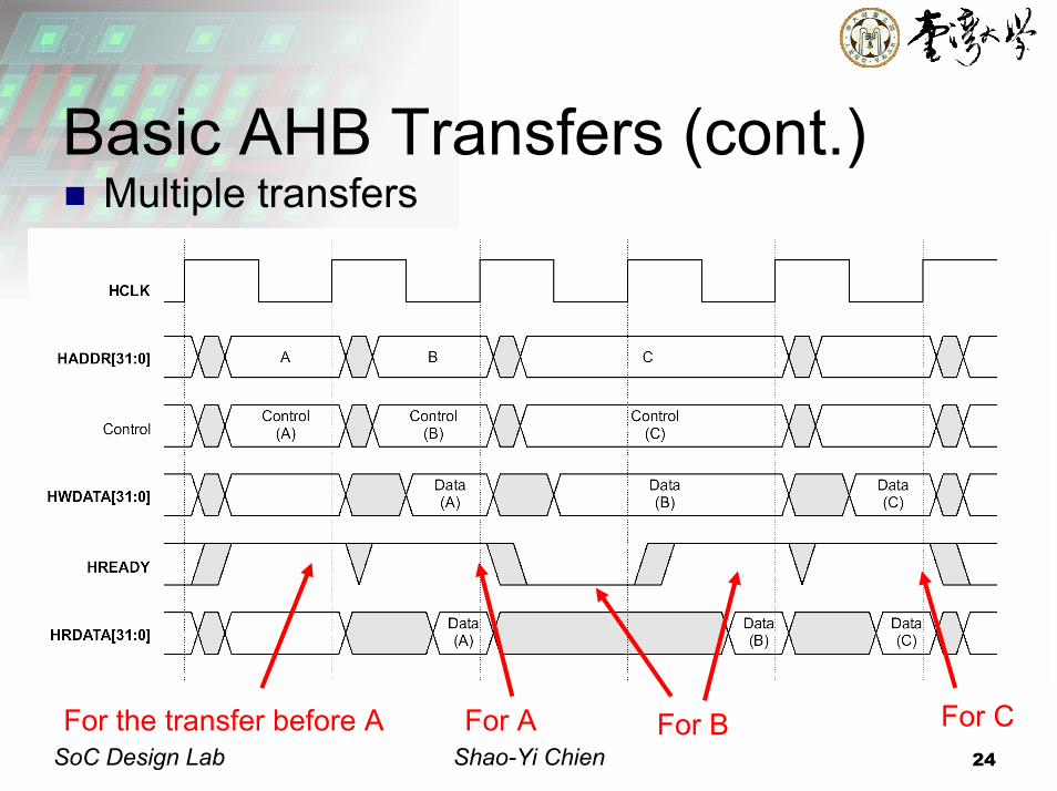
Basic AHB Transfers (cont.)Multiple transfers
For CFor the transfer before A For A For B
Shao-Yi Chien 25SoC Design Lab
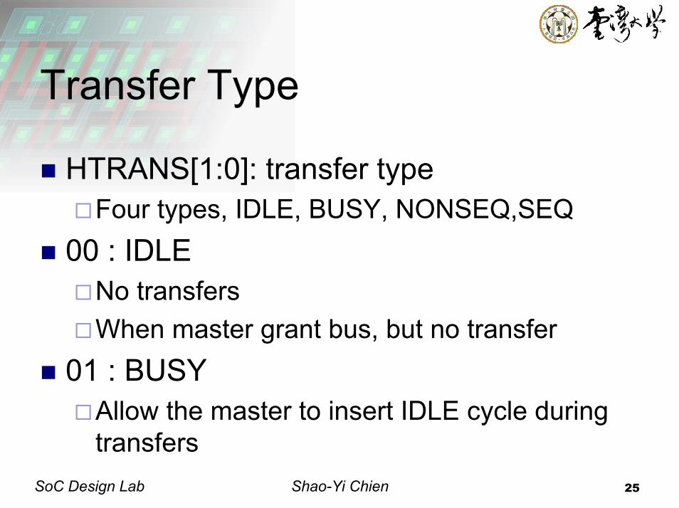
Transfer Type
HTRANS[1:0]: transfer typeFour types, IDLE, BUSY, NONSEQ,SEQ
00 : IDLENo transfersWhen master grant bus, but no transfer
01 : BUSYAllow the master to insert IDLE cycle during transfers
Shao-Yi Chien 26SoC Design Lab
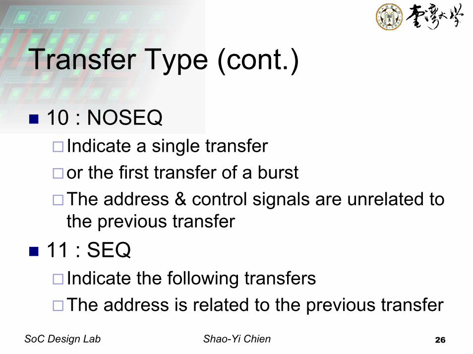
Transfer Type (cont.)
10 : NOSEQIndicate a single transferor the first transfer of a burstThe address & control signals are unrelated to the previous transfer
11 : SEQIndicate the following transfersThe address is related to the previous transfer
Shao-Yi Chien 27SoC Design Lab
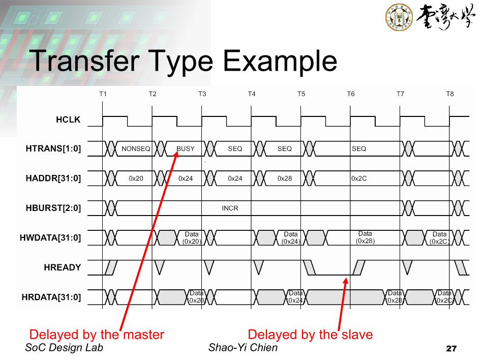
Transfer Type Example
Delayed by the master Delayed by the slave
Shao-Yi Chien 28SoC Design Lab
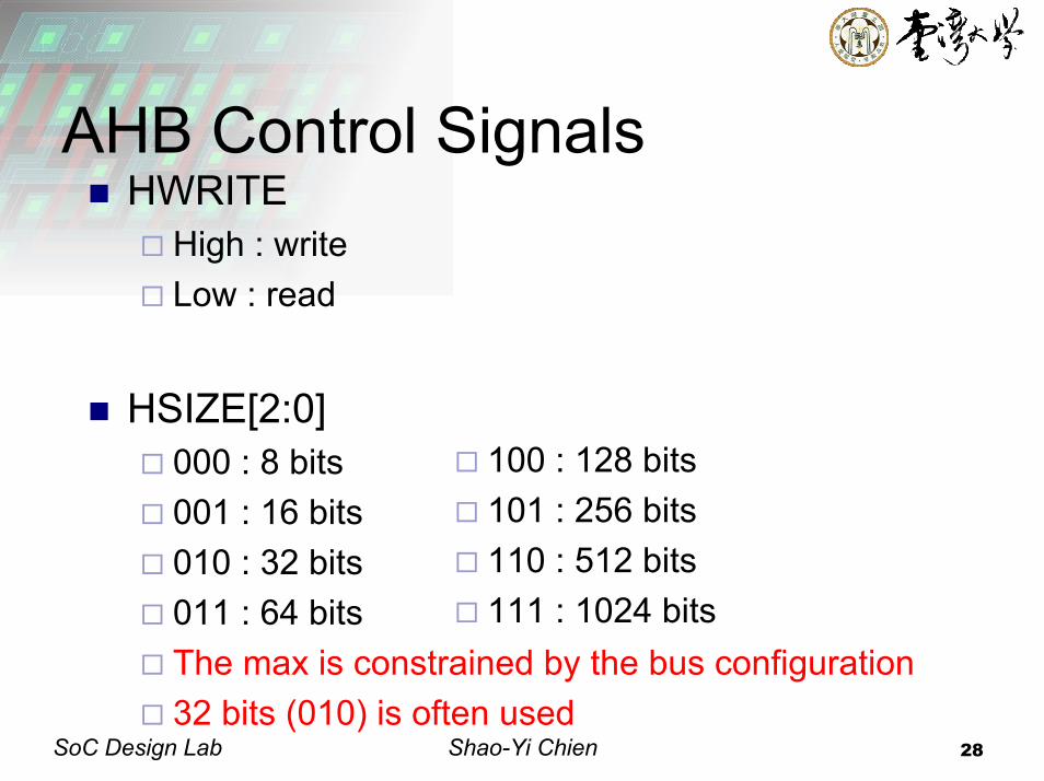
AHB Control SignalsHWRITE
High : writeLow : read
HSIZE[2:0]000 : 8 bits001 : 16 bits010 : 32 bits011 : 64 bitsThe max is constrained by the bus configuration32 bits (010) is often used
100 : 128 bits101 : 256 bits110 : 512 bits111 : 1024 bits
Shao-Yi Chien 29SoC Design Lab
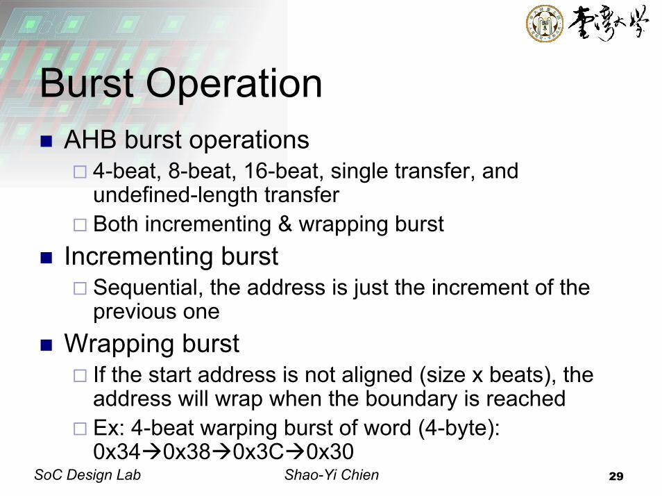
Burst OperationAHB burst operations
4-beat, 8-beat, 16-beat, single transfer, and undefined-length transferBoth incrementing & wrapping burst
Incrementing burstSequential, the address is just the increment of the previous one
Wrapping burstIf the start address is not aligned (size x beats), the address will wrap when the boundary is reachedEx: 4-beat warping burst of word (4-byte): 0x34 0x38 0x3C 0x30
Shao-Yi Chien 30SoC Design Lab
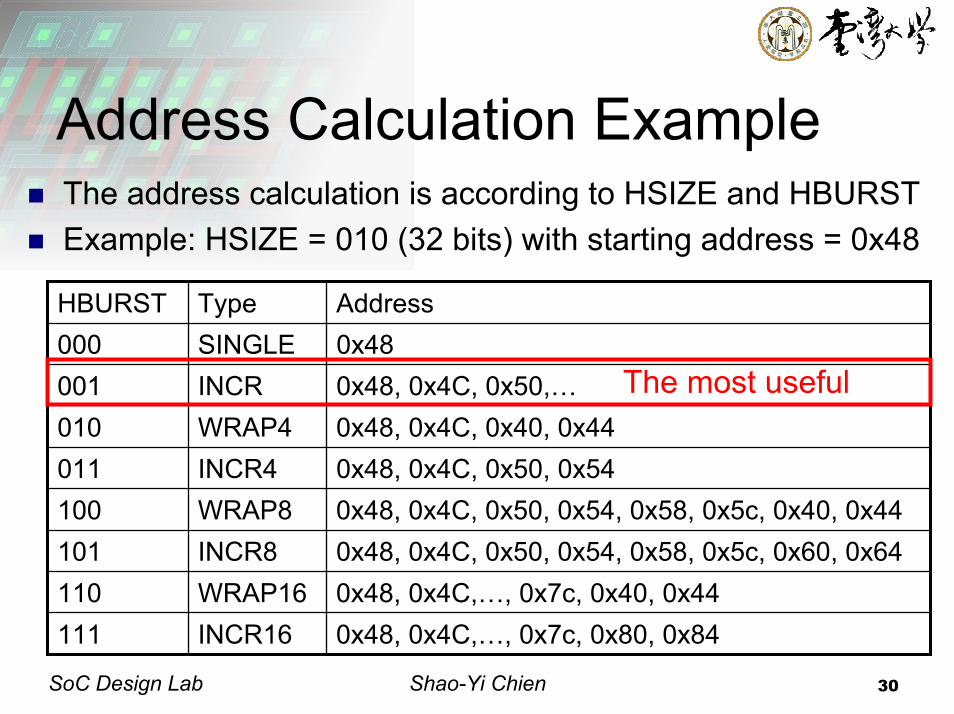
Address Calculation ExampleThe address calculation is according to HSIZE and HBURSTExample: HSIZE = 010 (32 bits) with starting address = 0x48
HBURST Type Address000 SINGLE 0x48001 INCR 0x48, 0x4C, 0x50,…010 WRAP4 0x48, 0x4C, 0x40, 0x44011 INCR4 0x48, 0x4C, 0x50, 0x54100 WRAP8 0x48, 0x4C, 0x50, 0x54, 0x58, 0x5c, 0x40, 0x44101 INCR8 0x48, 0x4C, 0x50, 0x54, 0x58, 0x5c, 0x60, 0x64110 WRAP16 0x48, 0x4C,…, 0x7c, 0x40, 0x44111 INCR16 0x48, 0x4C,…, 0x7c, 0x80, 0x84
The most useful
Shao-Yi Chien 31SoC Design Lab
Important!!
Burst transfer can’t cross the 1K boundaryBecause the minimal address range for a slave is 1 KBNONSEQ → SEQ → 1KB Boundary →NONSEQ → SEQ…
The master do not attempt to start a fixed-length incrementing burst which would cause this boundary to be crossed
Shao-Yi Chien 32SoC Design Lab
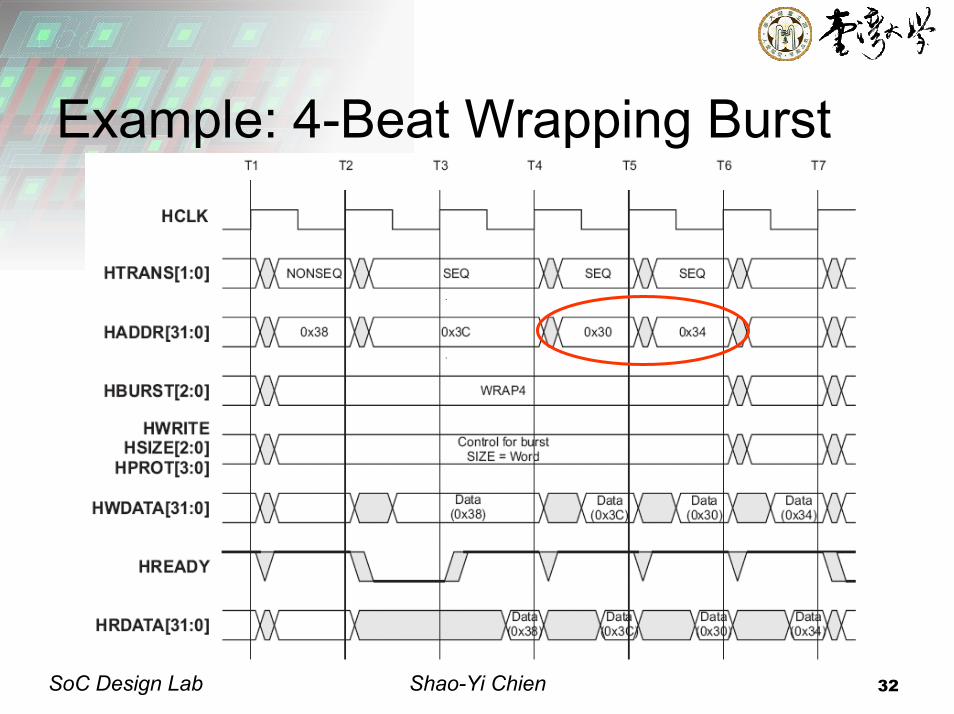
Example: 4-Beat Wrapping Burst
Shao-Yi Chien 33SoC Design Lab
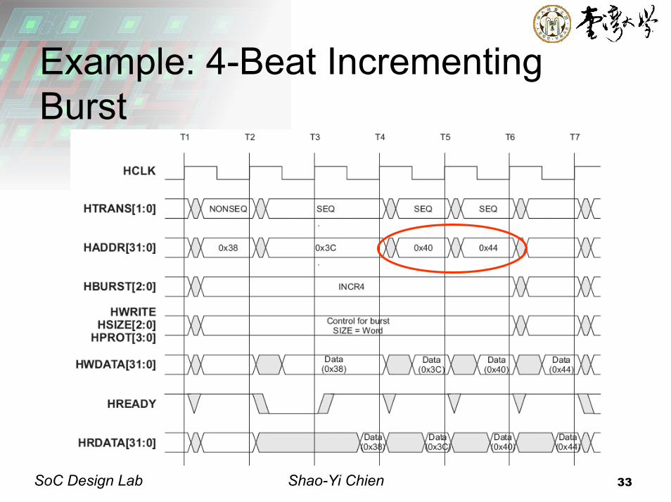
Example: 4-Beat Incrementing Burst
Shao-Yi Chien 34SoC Design Lab
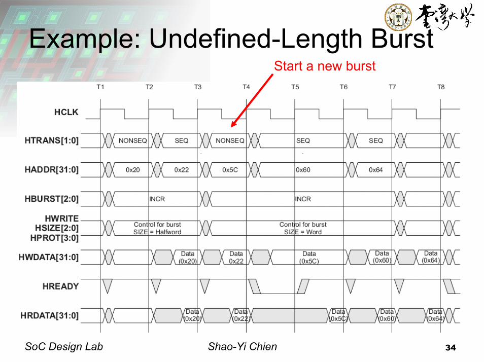
Example: Undefined-Length BurstStart a new burst
Shao-Yi Chien 35SoC Design Lab
Address Decoding
HSELx : slave selectIndicate the slave is selected by a master
A central address decoder is used to provide the select signalA slave should occupy at least 1KB of memory spaceAn additional default slave is used to fill up the memory map
Shao-Yi Chien 36SoC Design Lab
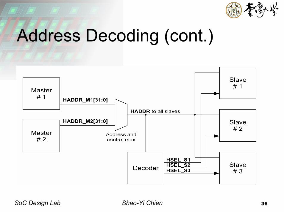
Address Decoding (cont.)
Shao-Yi Chien 37SoC Design Lab
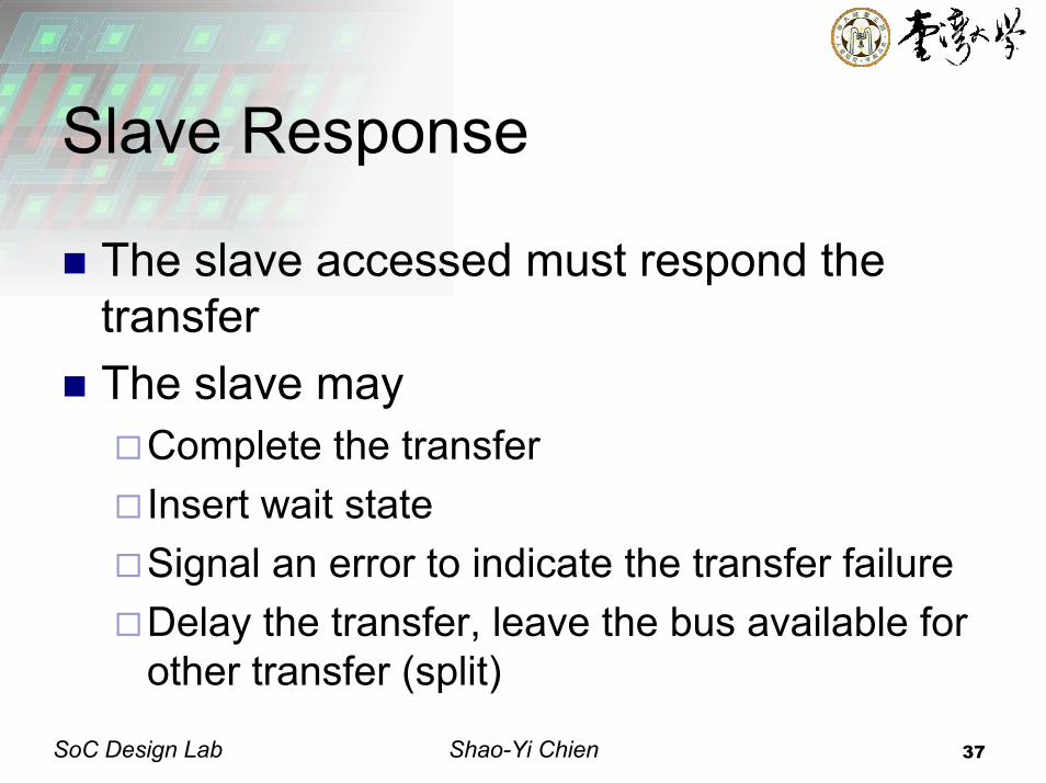
Slave Response
The slave accessed must respond the transferThe slave may
Complete the transferInsert wait stateSignal an error to indicate the transfer failureDelay the transfer, leave the bus available for other transfer (split)
Shao-Yi Chien 38SoC Design Lab
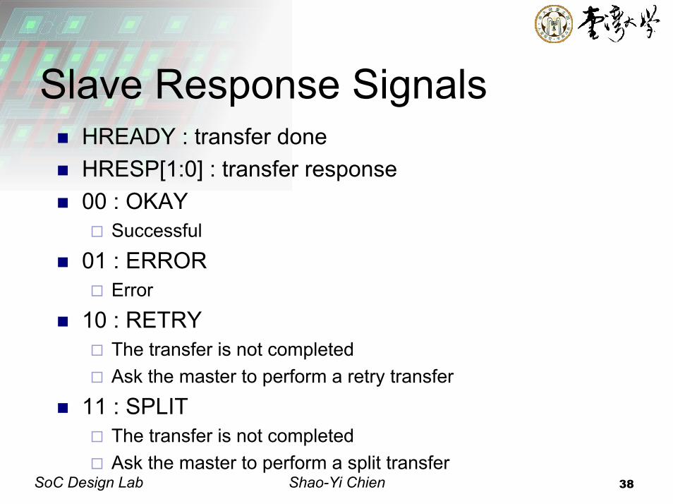
Slave Response SignalsHREADY : transfer doneHRESP[1:0] : transfer response00 : OKAY
Successful
01 : ERRORError
10 : RETRYThe transfer is not completedAsk the master to perform a retry transfer
11 : SPLITThe transfer is not completedAsk the master to perform a split transfer
Shao-Yi Chien 39SoC Design Lab
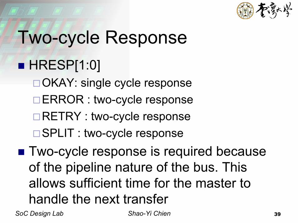
Two-cycle ResponseHRESP[1:0]
OKAY: single cycle responseERROR : two-cycle responseRETRY : two-cycle responseSPLIT : two-cycle response
Two-cycle response is required because of the pipeline nature of the bus. This allows sufficient time for the master to handle the next transfer
Shao-Yi Chien 40SoC Design Lab
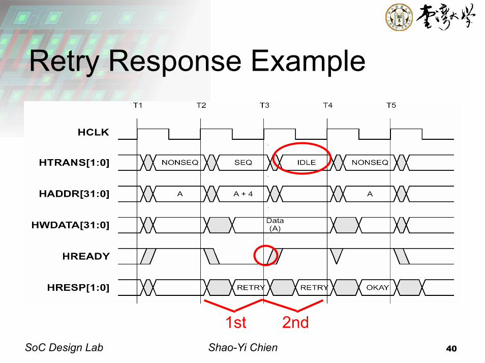
Retry Response Example
1st 2nd
Shao-Yi Chien 41SoC Design Lab
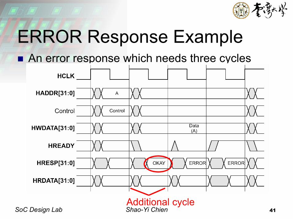
ERROR Response ExampleAn error response which needs three cycles
Additional cycle
Shao-Yi Chien 42SoC Design Lab
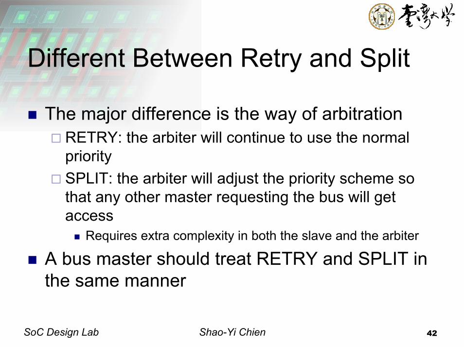
Different Between Retry and Split
The major difference is the way of arbitrationRETRY: the arbiter will continue to use the normal prioritySPLIT: the arbiter will adjust the priority scheme so that any other master requesting the bus will get access
Requires extra complexity in both the slave and the arbiter
A bus master should treat RETRY and SPLIT in the same manner
Shao-Yi Chien 43SoC Design Lab
Data BusNon-tri-state, separate read & write busesEndianness
Not specified in the AMBA spec.All the masters and slaves should of the same endiannessDynamic endianness is not supported
For IP design, only IPs which will be used in wide variety of applications should be made bi-endian
Shao-Yi Chien 44SoC Design Lab
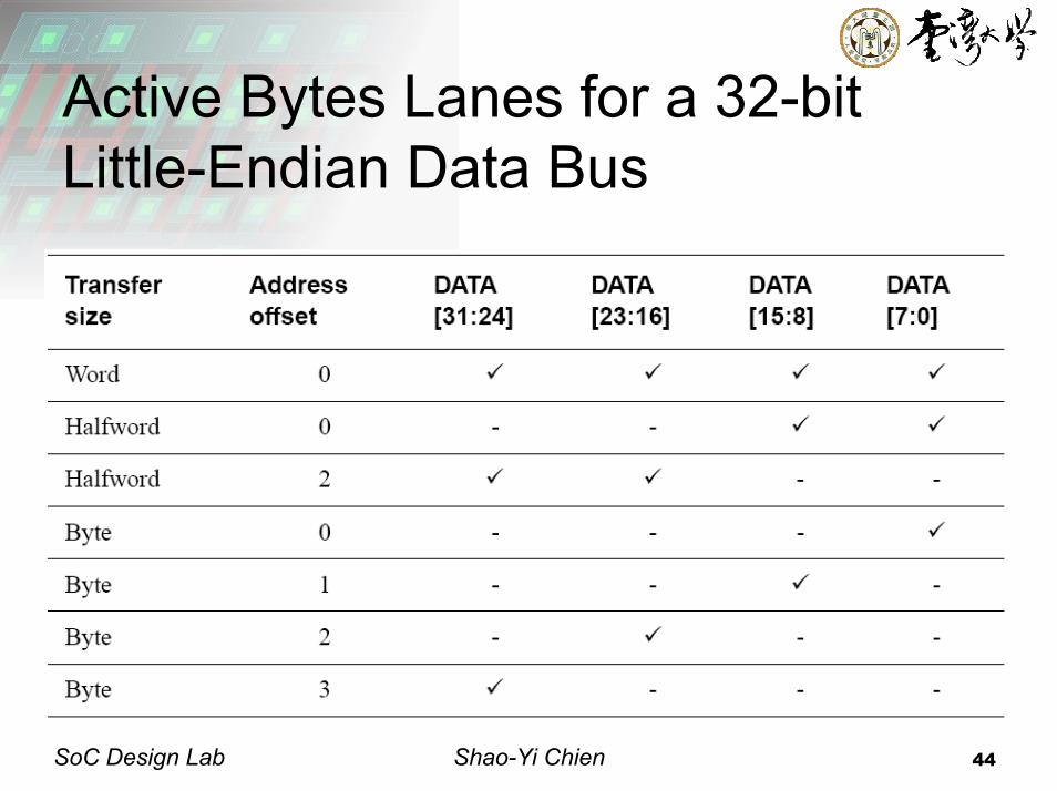
Active Bytes Lanes for a 32-bit Little-Endian Data Bus
Shao-Yi Chien 45SoC Design Lab
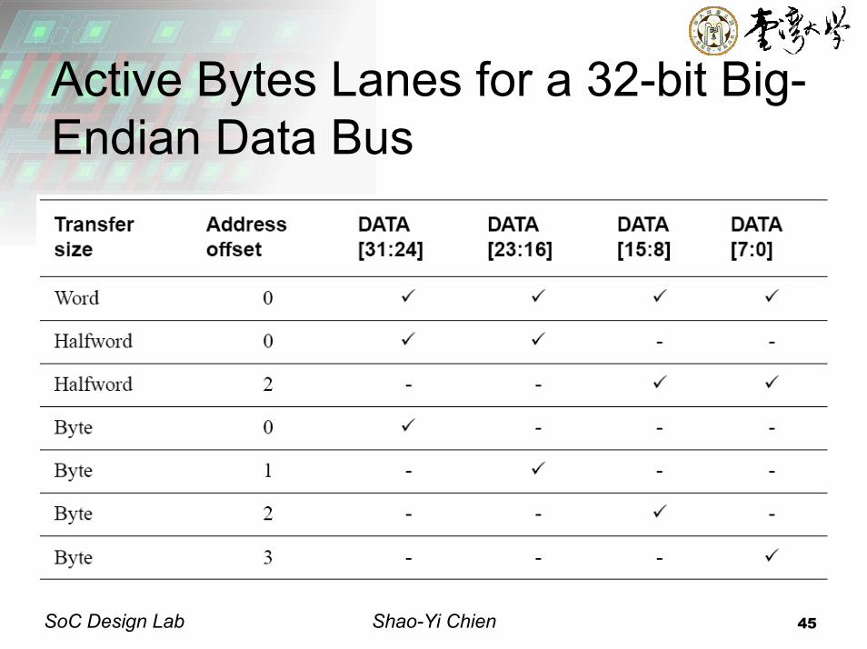
Active Bytes Lanes for a 32-bit Big-Endian Data Bus
Shao-Yi Chien 46SoC Design Lab
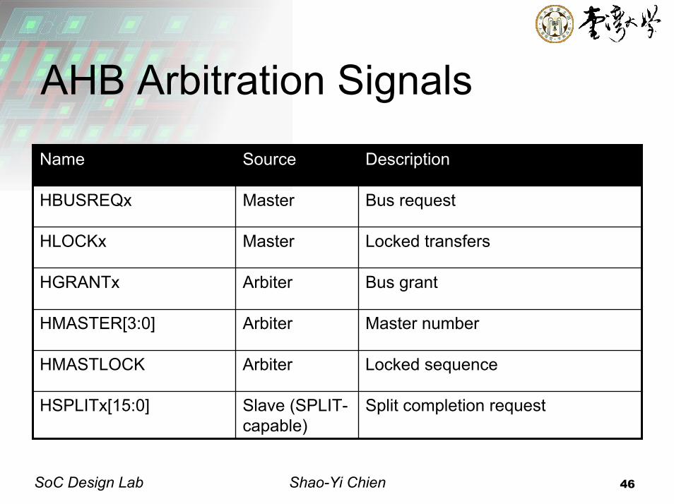
AHB Arbitration Signals
Name Source Description
HBUSREQx Master Bus request
HLOCKx Master Locked transfers
HGRANTx Arbiter Bus grant
HMASTER[3:0] Arbiter Master number
HMASTLOCK Arbiter Locked sequence
HSPLITx[15:0] Slave (SPLIT-capable)
Split completion request
Shao-Yi Chien 47SoC Design Lab
Arbitration Signals (cont.)HBUSREQ
Bus requestHLOCKx :
High: the master requires locked access to the bus
HGRANTxIndicate the master x accessible to the busMaster x gains ownership: HGRANTx=1 & HREADY=1
Shao-Yi Chien 48SoC Design Lab
Arbitration Signals (cont.)HMASTER[3:0]
Indicate which master is transferring, information for splitting
HMASTLOCKIndicate the master is performing a locked transfer
HSPLITx[15:0]Used by the slave to indicate the arbiter which master should be allowed to re-attempt a split transactionEach bit corresponds to a single master
Shao-Yi Chien 49SoC Design Lab
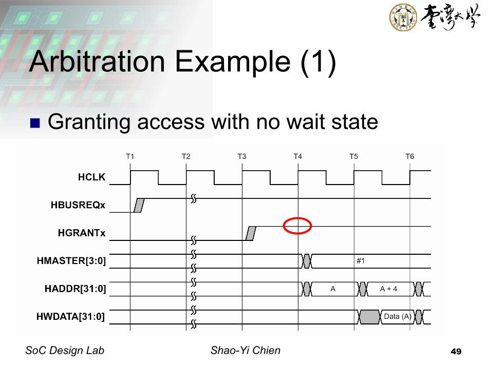
Arbitration Example (1)
Granting access with no wait state
Shao-Yi Chien 50SoC Design Lab
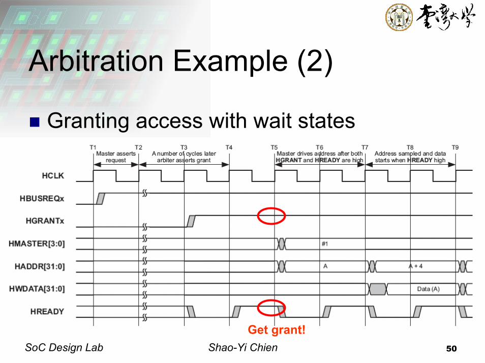
Arbitration Example (2)
Granting access with wait states
Get grant!
Shao-Yi Chien 51SoC Design Lab
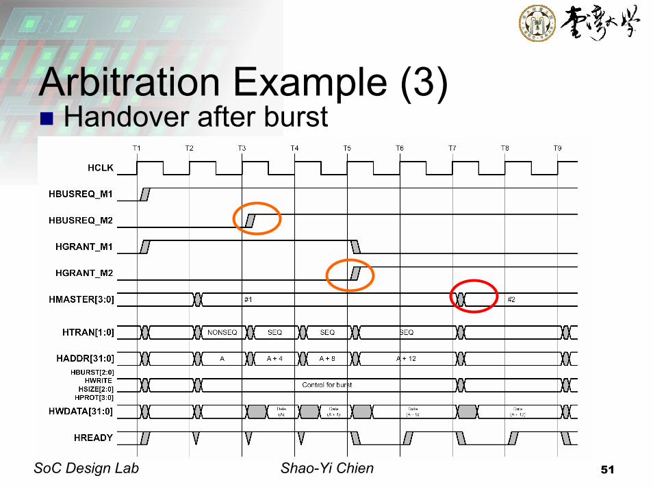
Arbitration Example (3)Handover after burst
Shao-Yi Chien 52SoC Design Lab
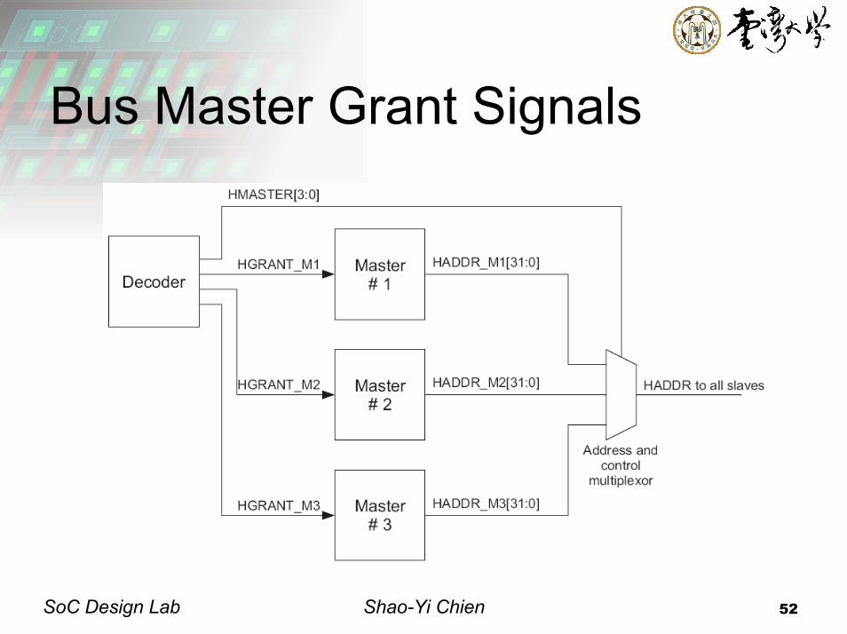
Bus Master Grant Signals
Shao-Yi Chien 53SoC Design Lab
Notes
For a fixed length burst, it is not necessary to continue request the busFor a undefined length burst, the master should continue to assert the request until it has started the last transferIf no master requests the bus, grant to the default master with HTRANS=IDLEIt is recommended that the master inserts an IDLE transfer after any locked sequence to provide the opportunity for changing arbitration
Shao-Yi Chien 54SoC Design Lab
Split Transfer SequenceThe master starts the transfer.If the slave decides that it may take a number of cycles to obtain the data, it gives a SPLIT transfer response. The slave record the master number, HMASTER. Then the arbiter change the priority of the masters.The arbiter grants other masters, bus master handover.When the slave is ready to complete the transfer, it asserts the appropriate bit of the HSPLITx bus to the arbiter.The arbiter restores the priorityThe arbiter will grant the master so it can re-attempt the transferFinish
Shao-Yi Chien 55SoC Design Lab
Preventing DeadlockIt is possible for deadlock if a number of different masters attempt to access a slave which issues SPLIT or RETRY
The slave can withstand a request from every master in the system, up to a maximum of 16. It only needs to record the master number. (can ignore address and control)A slave which issues RETRY responses must only be accessed by one master at a time.
Some hardware protection mechanisms, such as ERROR message, can be used.
Shao-Yi Chien 56SoC Design Lab
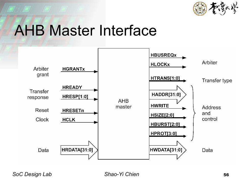
AHB Master Interface
Shao-Yi Chien 57SoC Design Lab
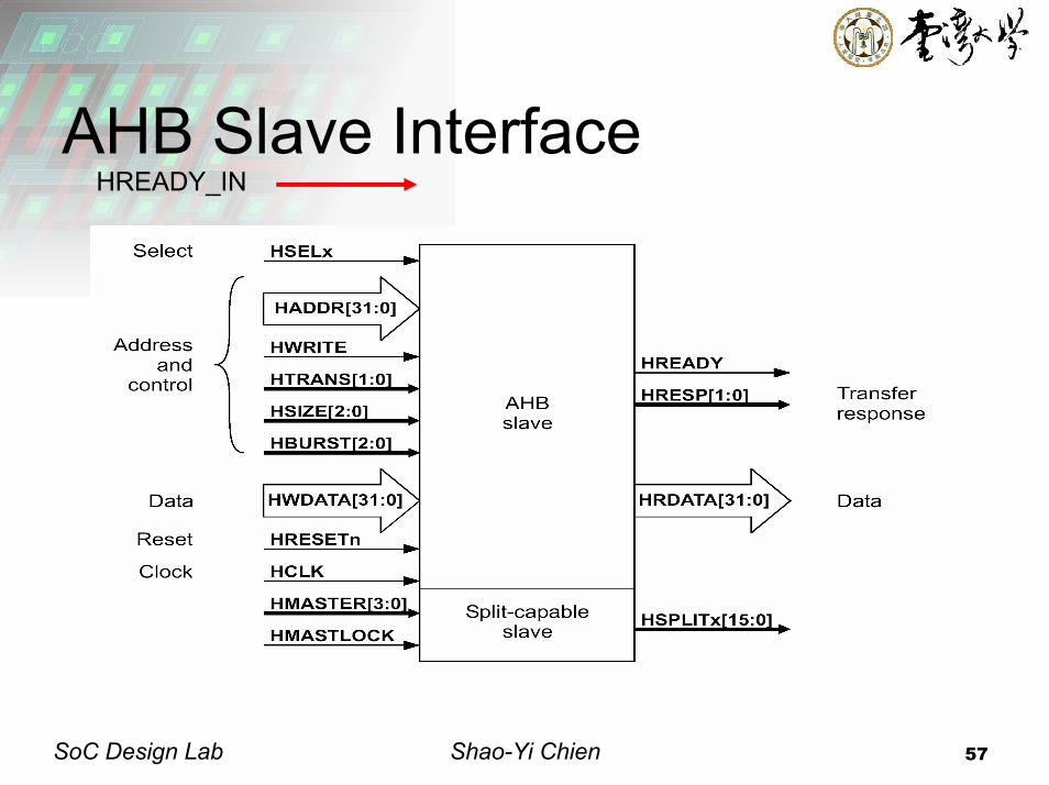
AHB Slave InterfaceHREADY_IN
Shao-Yi Chien 58SoC Design Lab
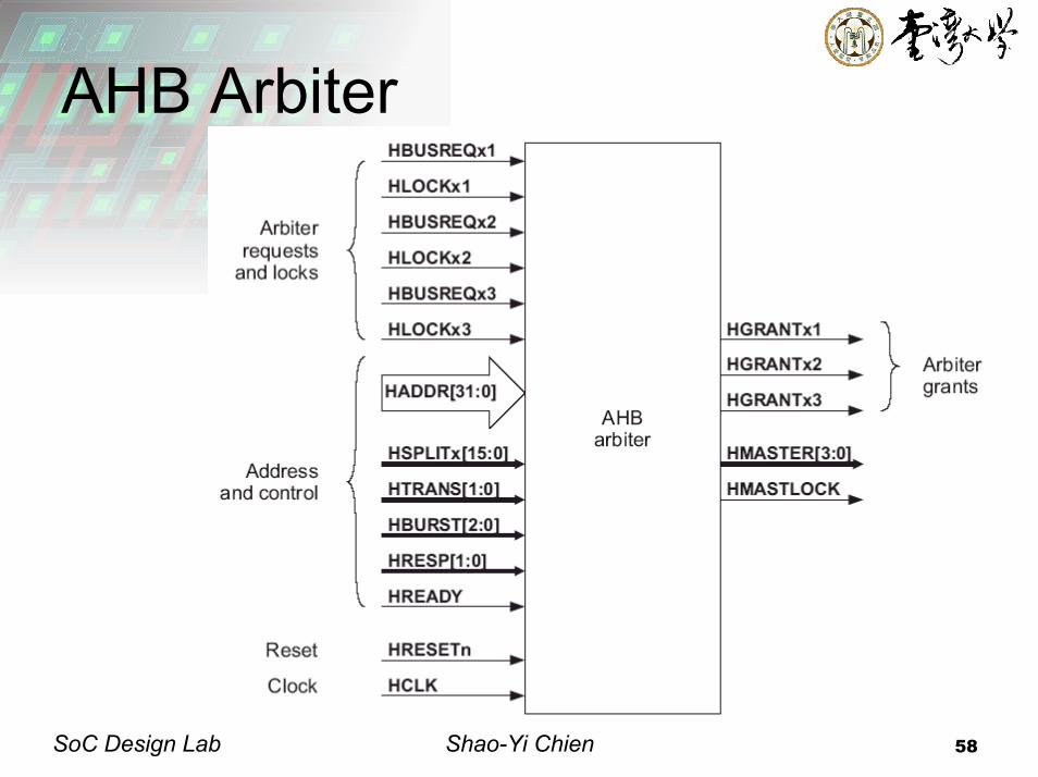
AHB Arbiter
Shao-Yi Chien 59SoC Design Lab
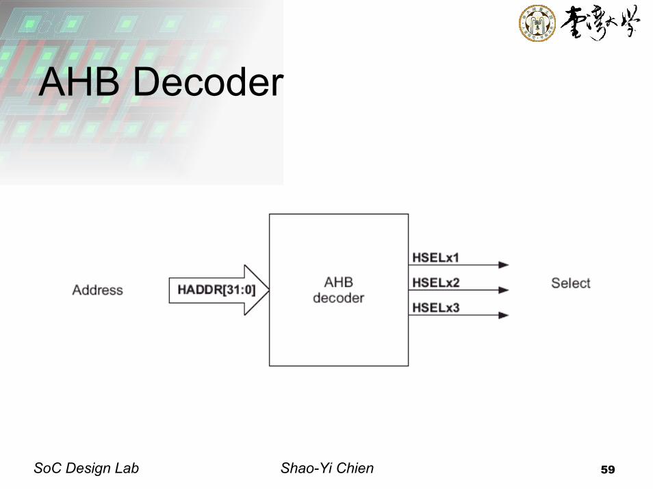
AHB Decoder
Shao-Yi Chien 60SoC Design Lab
Review on AHB
Main componentsMaster, slaves, arbiter, decoder
How the transfer progressThe pipelined scheme
How to increase the performanceBurst read/write
ArbitrationBus ownership handover
Shao-Yi Chien 61SoC Design Lab
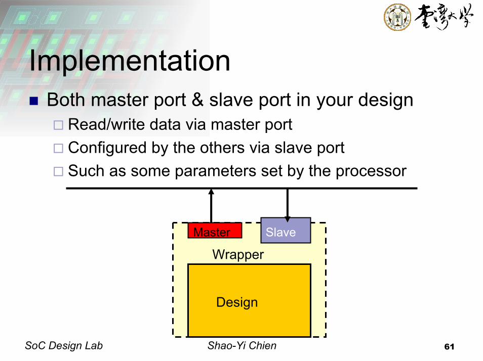
ImplementationBoth master port & slave port in your design
Read/write data via master portConfigured by the others via slave portSuch as some parameters set by the processor
Design
Wrapper
Master Slave
Shao-Yi Chien 62SoC Design Lab
Outline
OverviewAHBAPBTest methodology
Shao-Yi Chien 63SoC Design Lab
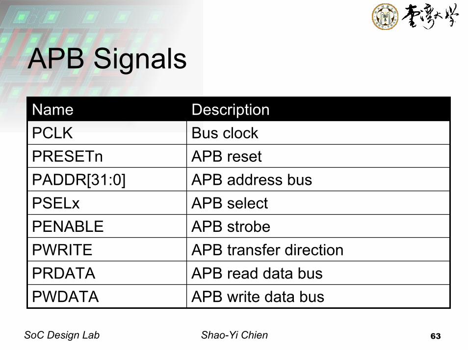
APB SignalsName DescriptionPCLK Bus clockPRESETn APB resetPADDR[31:0] APB address busPSELx APB selectPENABLE APB strobePWRITE APB transfer directionPRDATA APB read data busPWDATA APB write data bus
Shao-Yi Chien 64SoC Design Lab
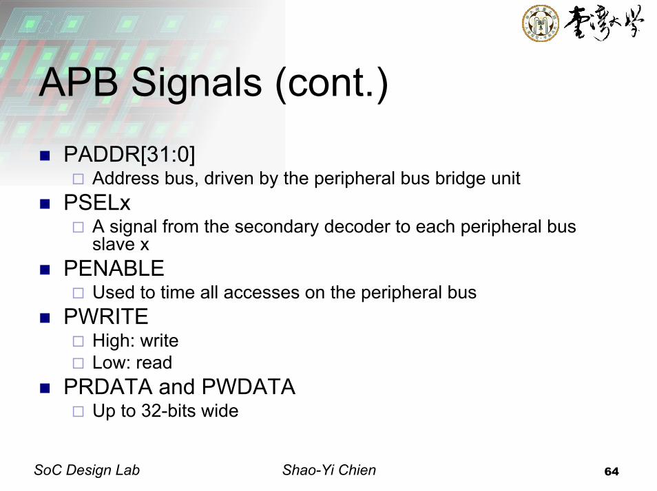
APB Signals (cont.)PADDR[31:0]
Address bus, driven by the peripheral bus bridge unitPSELx
A signal from the secondary decoder to each peripheral bus slave x
PENABLEUsed to time all accesses on the peripheral bus
PWRITEHigh: writeLow: read
PRDATA and PWDATAUp to 32-bits wide
Shao-Yi Chien 65SoC Design Lab
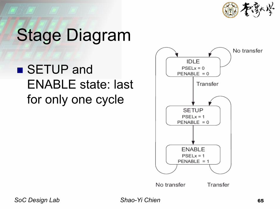
Stage Diagram
SETUP and ENABLE state: last for only one cycle
Shao-Yi Chien 66SoC Design Lab
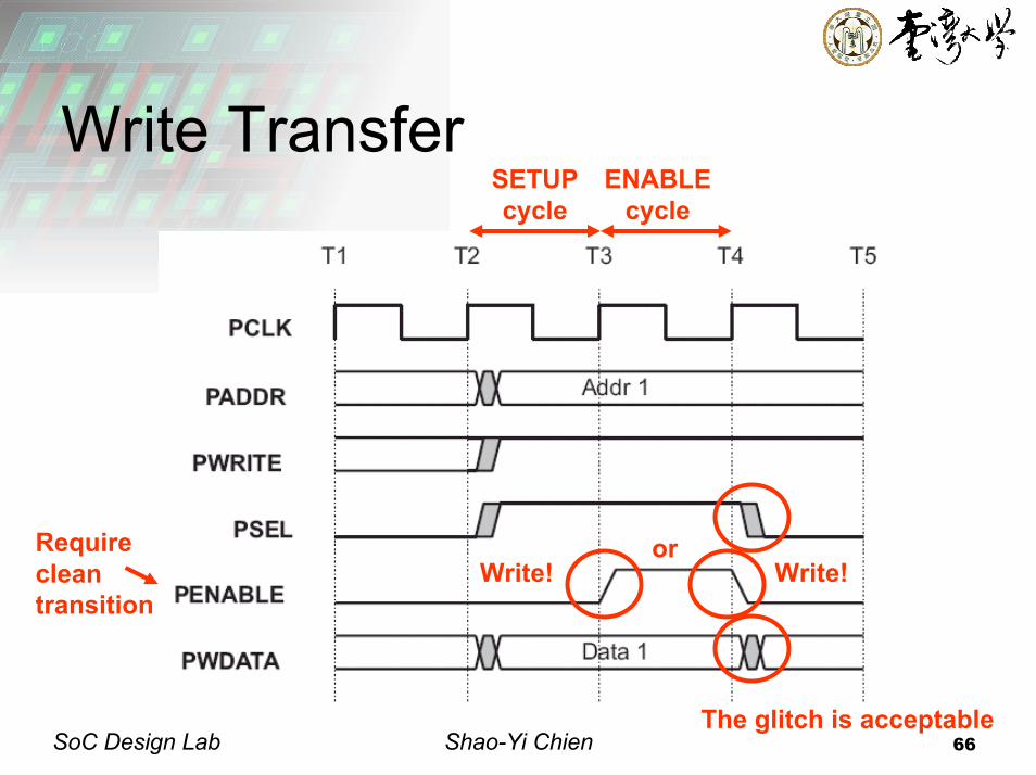
Write Transfer
The glitch is acceptable
SETUP cycle
ENABLE cycle
Require clean transition
Write! Write!or
Shao-Yi Chien 67SoC Design Lab
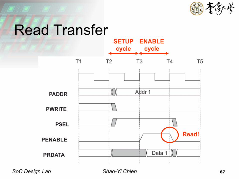
Read TransferSETUP cycle
ENABLE cycle
Read!
Shao-Yi Chien 68SoC Design Lab
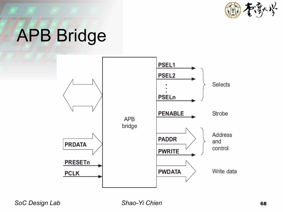
APB Bridge
Shao-Yi Chien 69SoC Design Lab
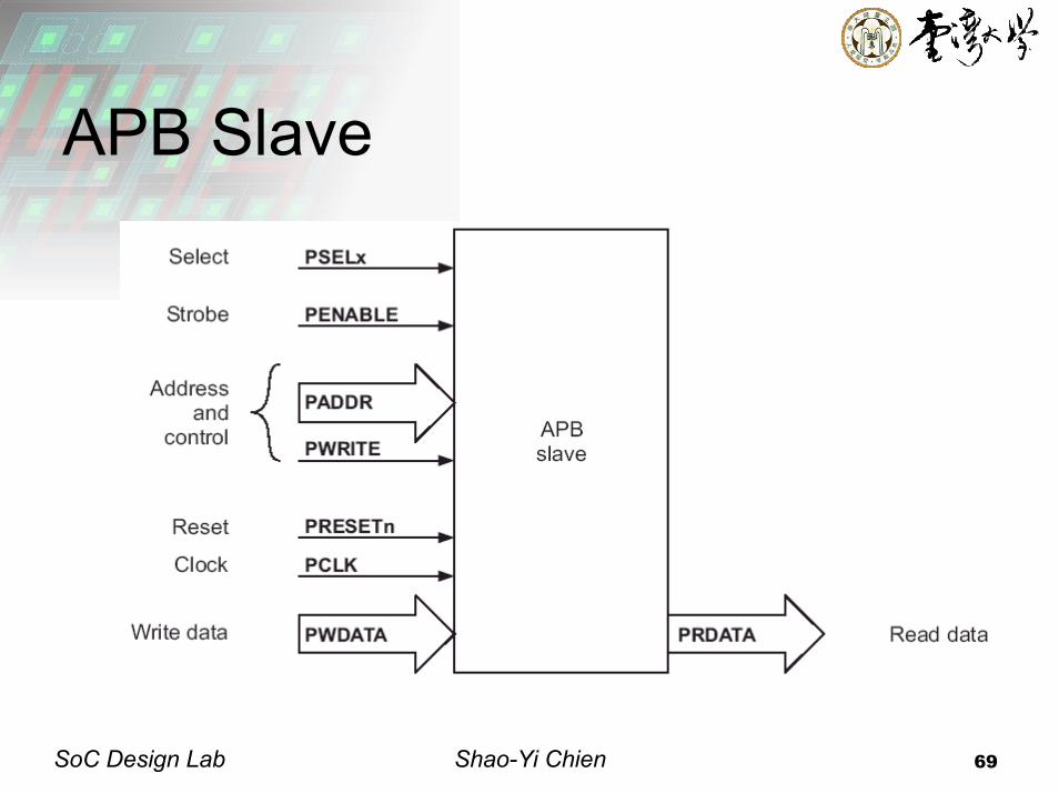
APB Slave
Shao-Yi Chien 70SoC Design Lab
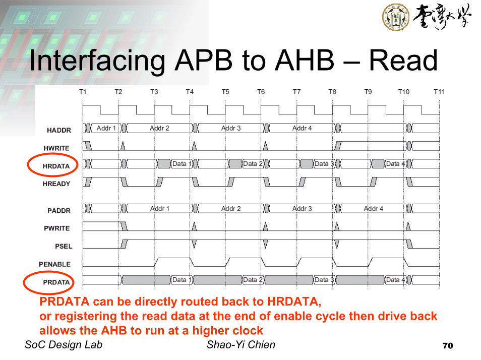
Interfacing APB to AHB – Read
PRDATA can be directly routed back to HRDATA,or registering the read data at the end of enable cycle then drive back allows the AHB to run at a higher clock
Shao-Yi Chien 71SoC Design Lab
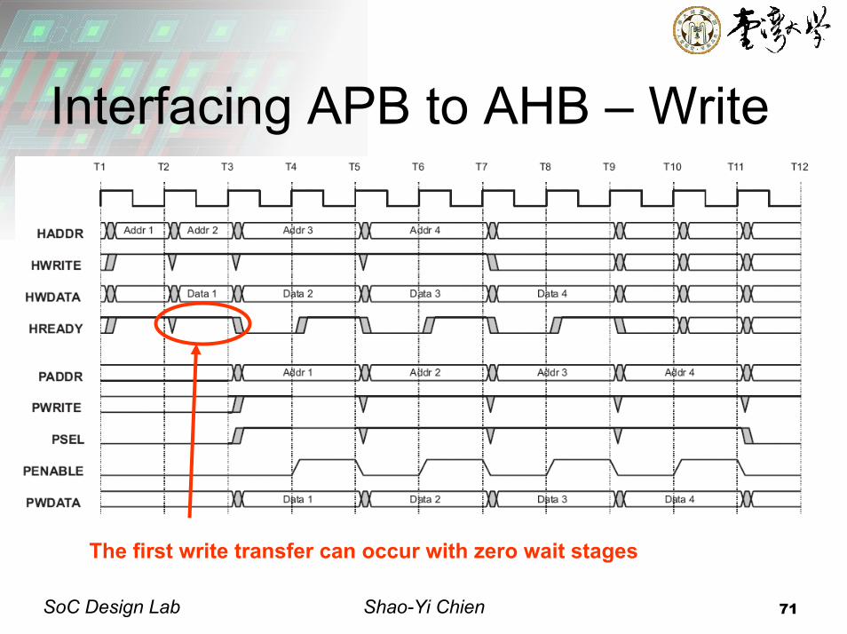
Interfacing APB to AHB – Write
The first write transfer can occur with zero wait stages
Shao-Yi Chien 72SoC Design Lab
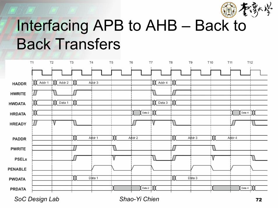
Interfacing APB to AHB – Back to Back Transfers
Shao-Yi Chien 73SoC Design Lab
Outline
OverviewAHBAPBTest methodology
Shao-Yi Chien 74SoC Design Lab
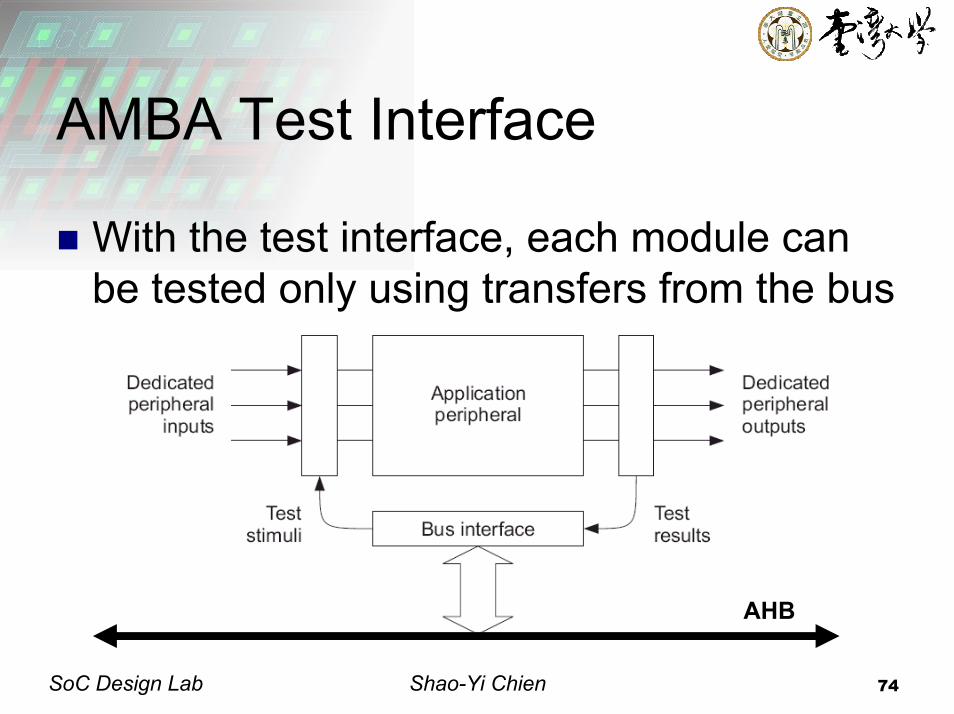
AMBA Test Interface
With the test interface, each module can be tested only using transfers from the bus
AHB
Shao-Yi Chien 75SoC Design Lab
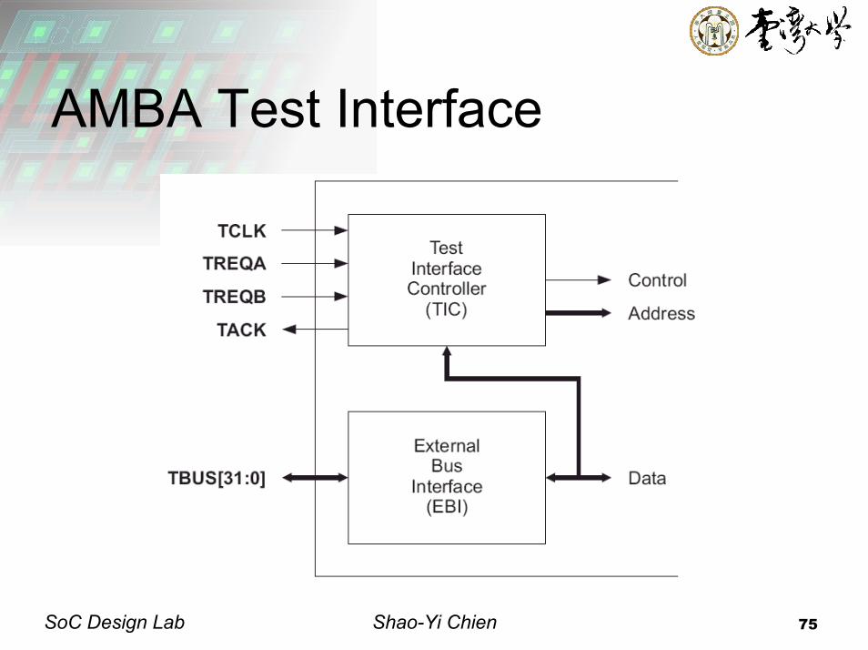
AMBA Test Interface
Shao-Yi Chien 76SoC Design Lab
Signals for Test InterfaceTCLK
Test clockAssigned HCLK during test mode
TREQATest burst request A, is required as a dedicated device pinUsed to request entry into the test mode
TREQBTREQA/TREQA can indicate the type of test vector
TACKTest acknowledge, required as a dedicated device pinTREQA and TREQB signals are only sampled by the TIC when TACK is HIGH
Shao-Yi Chien 77SoC Design Lab
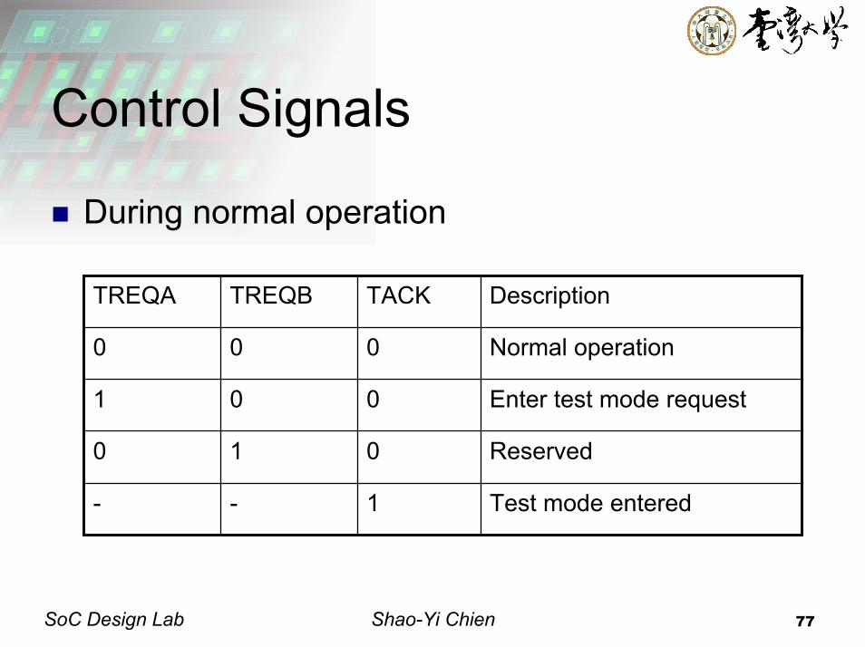
Control Signals
During normal operation
TREQA TREQB TACK Description
0 0 0 Normal operation
1 0 0 Enter test mode request
0 1 0 Reserved
- - 1 Test mode entered
Shao-Yi Chien 78SoC Design Lab
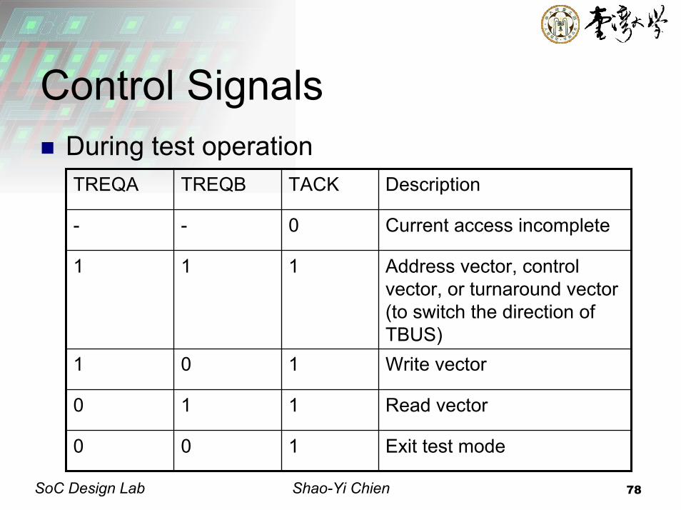
Control SignalsDuring test operationTREQA TREQB TACK Description
- - 0 Current access incomplete
1 1 1 Address vector, control vector, or turnaround vector (to switch the direction of TBUS)
1 0 1 Write vector
0 1 1 Read vector
0 0 1 Exit test mode
Shao-Yi Chien 79SoC Design Lab
How to Distinguish Address, Control, and Turnaround Vectors?
Single address/control vector is address vectorBurst of address/control vectors are all address vectors, but the last one is control vectorA read vector, or burst of read vectors, is always followed by a turnaround vector(AHB requires two turnaround vectors)
Shao-Yi Chien 80SoC Design Lab
Incremental Addressing
The TIC may support incrementing of the bus addressA typical implementation would use an 8-bit address incrementer, up to 1kB boundaryOnly supports undefined-length transfer
Shao-Yi Chien 81SoC Design Lab
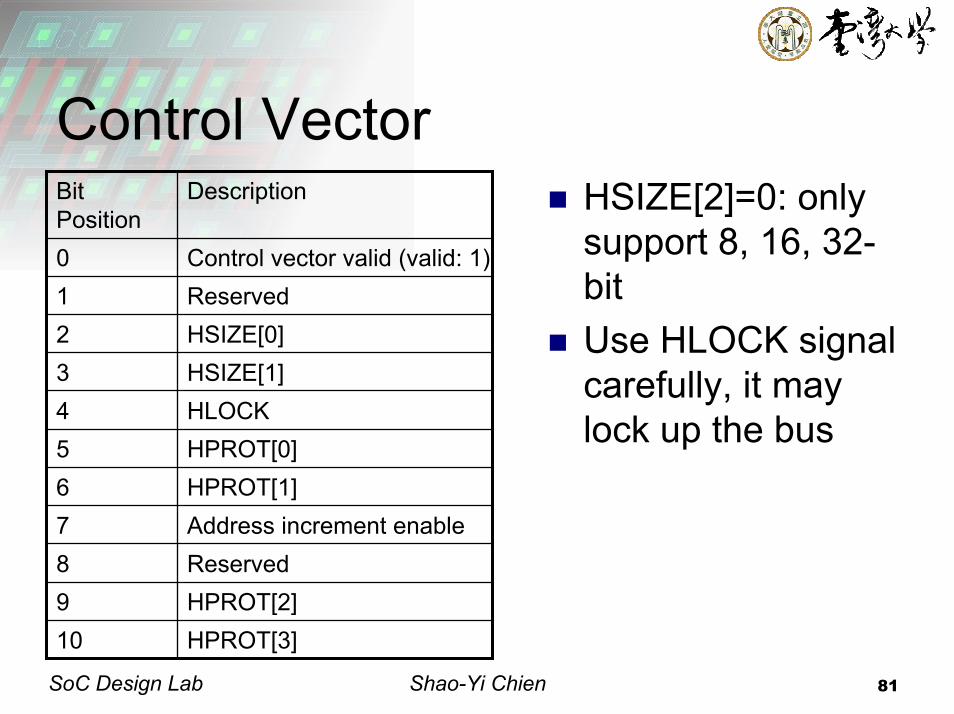
Control VectorBit Position
Description
0 Control vector valid (valid: 1)1 Reserved2 HSIZE[0]3 HSIZE[1]4 HLOCK5 HPROT[0]6 HPROT[1]7 Address increment enable8 Reserved9 HPROT[2]10 HPROT[3]
HSIZE[2]=0: only support 8, 16, 32-bitUse HLOCK signal carefully, it may lock up the bus
Shao-Yi Chien 82SoC Design Lab
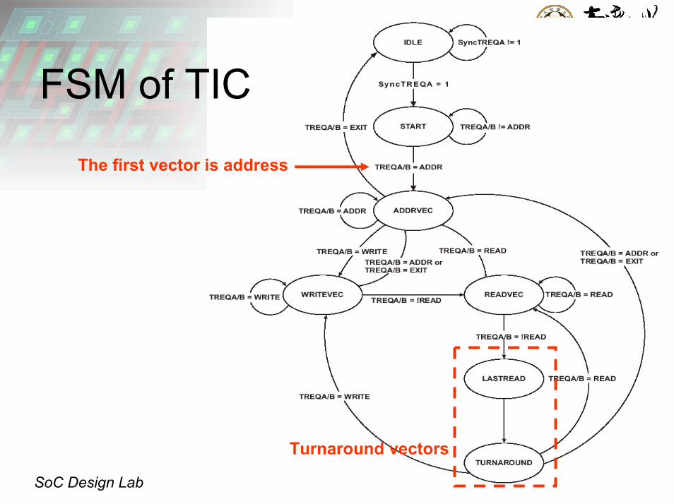
FSM of TIC
Turnaround vectors
The first vector is address
Shao-Yi Chien 83SoC Design Lab
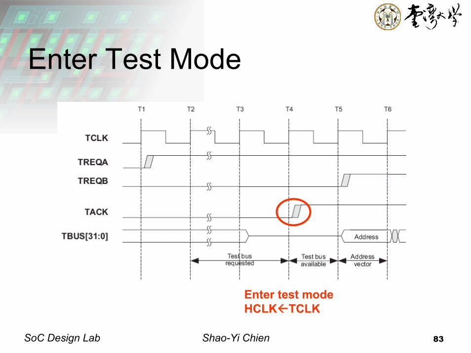
Enter Test Mode
Enter test modeHCLK TCLK
Shao-Yi Chien 84SoC Design Lab
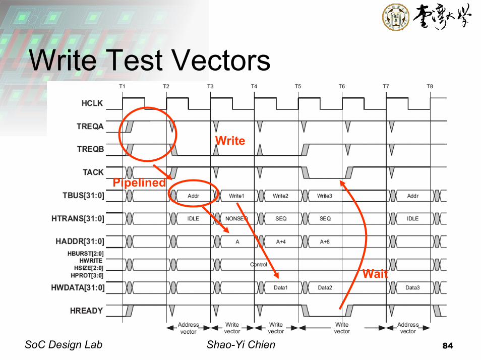
Write Test Vectors
Pipelined
Write
Wait
Shao-Yi Chien 85SoC Design Lab
Read Test Vectors
Tri-state
There must be a tri-state after address and read vector
Wait
LASTREADTURNAROUND
Tri-state
Shao-Yi Chien 86SoC Design Lab
Control Vector
Shao-Yi Chien 87SoC Design Lab
Read-to-Write and Write-to-Read
Read Write
Shao-Yi Chien 88SoC Design Lab
Other Topics
AHB-LiteMulti-layer AHB
Shao-Yi Chien 89SoC Design Lab
AHB-Lite
AHB-LiteA subset of the full AHB specificationOnly one single bus master usedNo need of the request/grant protocol to the arbiterNo arbiter No Retry/Split response from slavesNo master-to-slave multiplexor
Shao-Yi Chien 90SoC Design Lab
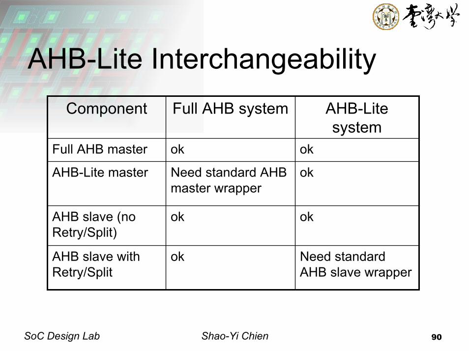
AHB-Lite InterchangeabilityComponent Full AHB system AHB-Lite
systemFull AHB master ok ok
AHB-Lite master Need standard AHB master wrapper
ok
AHB slave (no Retry/Split)
ok ok
AHB slave with Retry/Split
ok Need standard AHB slave wrapper
Shao-Yi Chien 91SoC Design Lab
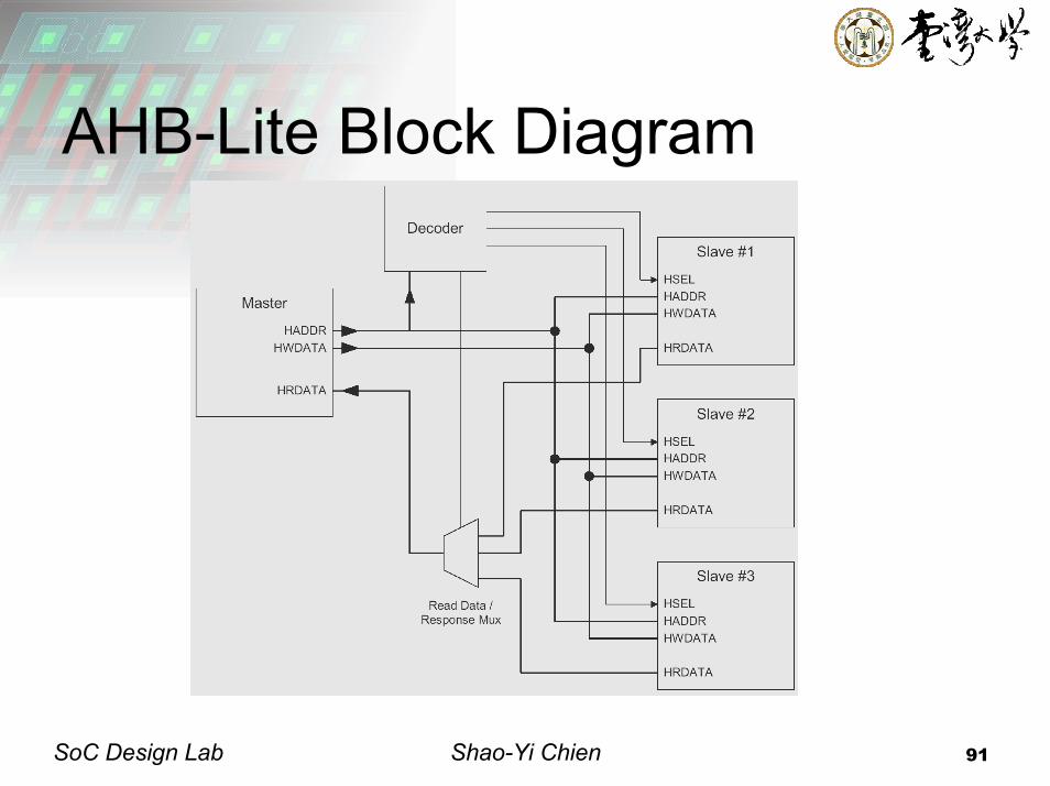
AHB-Lite Block Diagram
Shao-Yi Chien 92SoC Design Lab
Multi-layer AHB
Multi-layer AHBEnables parallel access paths between multiple masters and slaves by an interconnection matrixIncrease the overall bus bandwidthMore flexible system architecture
Make slaves local to a particular layerMake multiple slaves appear as a single slave to the interconnection matrixMultiple masters on a single layer
Shao-Yi Chien 93SoC Design Lab
Multi-layer AHBA simple multi-layer system
Shao-Yi Chien 94SoC Design Lab
Multi-layer AHBLocal slaves
Slave #4 and Slave #5 can only be accessed by Master #2
Shao-Yi Chien 95SoC Design Lab
Multi-layer AHB
Multiple slaves on one slave port
Combine low-bandwidth slaves togetherCombine salves usually accessed by the same master together
Shao-Yi Chien 96SoC Design Lab
Multi-layer AHB
Multiple masters on one layer
Combine masters which have low-bandwidth requirements togetherCombine special masters together
97
Communications Communications between Different between Different IPsIPs
Shao-Yi Chien 98SoC Design Lab
Communications
CPU (master) IP (slave)IP (master) IP (slave)
Shao-Yi Chien 99SoC Design Lab
Memory Mapped I/O
Each slave occupies a range of (>1KB) address space in the systemAll the slaves are addressableMemory mapped register/memoryCPU/IP and read/write data to other IP as read/write data from/to memory
Shao-Yi Chien 100SoC Design Lab
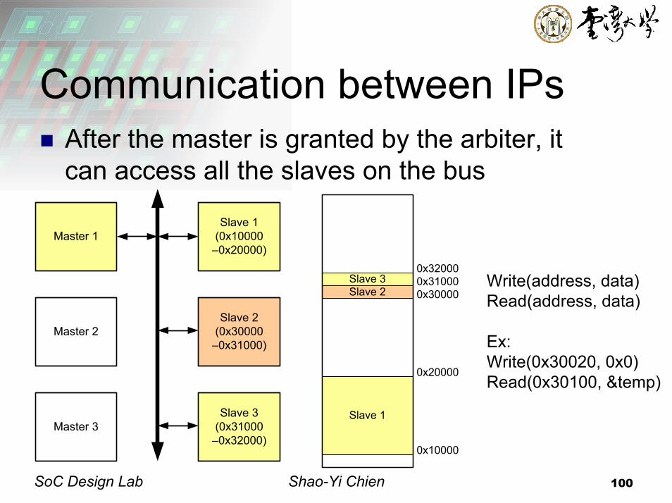
Communication between IPsAfter the master is granted by the arbiter, it can access all the slaves on the bus
Master 1
Master 2
Master 3
Slave 1(0x10000–0x20000)
Slave 2(0x30000–0x31000)
Slave 3(0x31000–0x32000)
Write(address, data)Read(address, data)
Ex:Write(0x30020, 0x0)Read(0x30100, &temp)
0x10000
0x20000
0x300000x310000x32000
Slave 1
Slave 2Slave 3
Shao-Yi Chien 101SoC Design Lab
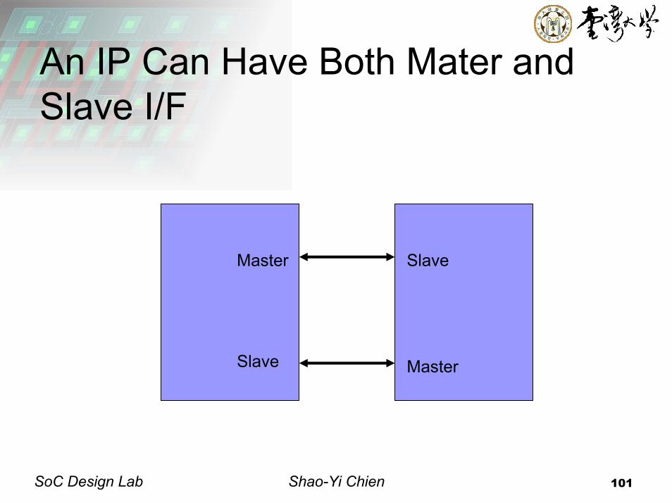
An IP Can Have Both Mater and Slave I/F
Master
Slave
Slave
Master
Shao-Yi Chien 102SoC Design Lab
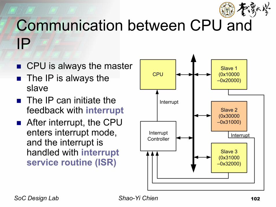
Communication between CPU and IP
CPU is always the masterThe IP is always the slaveThe IP can initiate the feedback with interruptAfter interrupt, the CPU enters interrupt mode, and the interrupt is handled with interrupt service routine (ISR)
CPU
InterruptController
Slave 1(0x10000
–0x20000)
Slave 2(0x30000
–0x31000)
Slave 3(0x31000
–0x32000)
Interrupt
Interrupt
Shao-Yi Chien 103SoC Design Lab
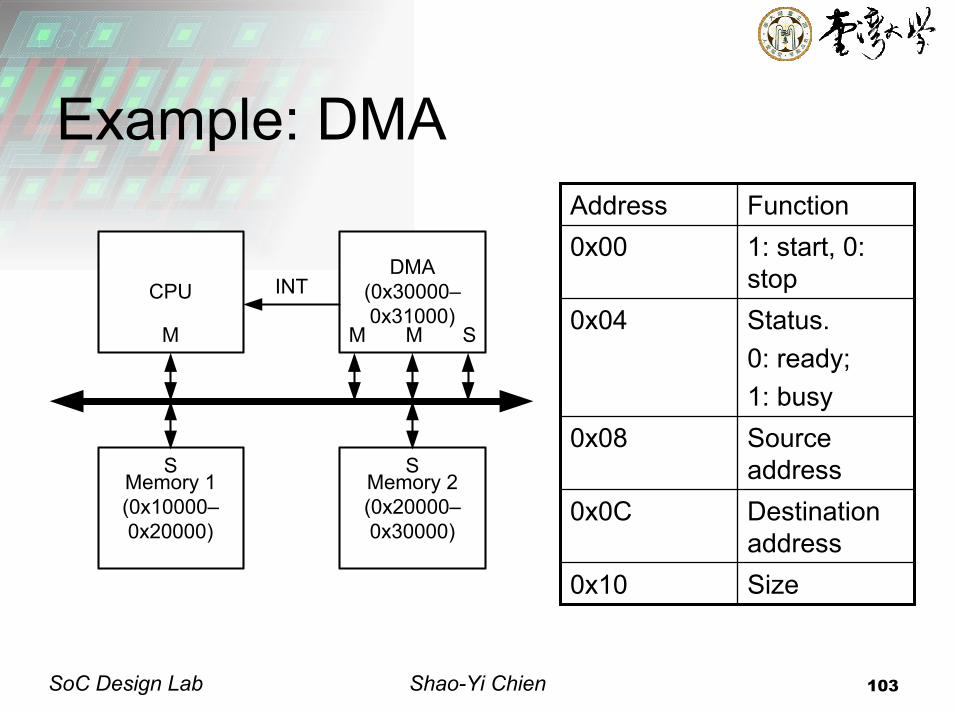
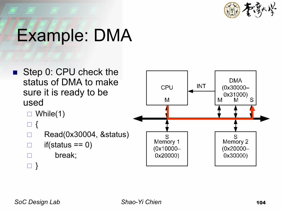
Example: DMA
CPU
M
DMA(0x30000–0x31000)
M M S
Memory 1(0x10000–0x20000)
Memory 2(0x20000–0x30000)
S S
INT
Address Function0x00 1: start, 0:
stop0x04 Status.
0: ready;1: busy
0x08 Source address
0x0C Destination address
0x10 Size
Shao-Yi Chien 104SoC Design Lab
Example: DMA
Step 0: CPU check the status of DMA to make sure it is ready to be used
While(1){
Read(0x30004, &status)if(status == 0)
break;}
Shao-Yi Chien 105SoC Design Lab
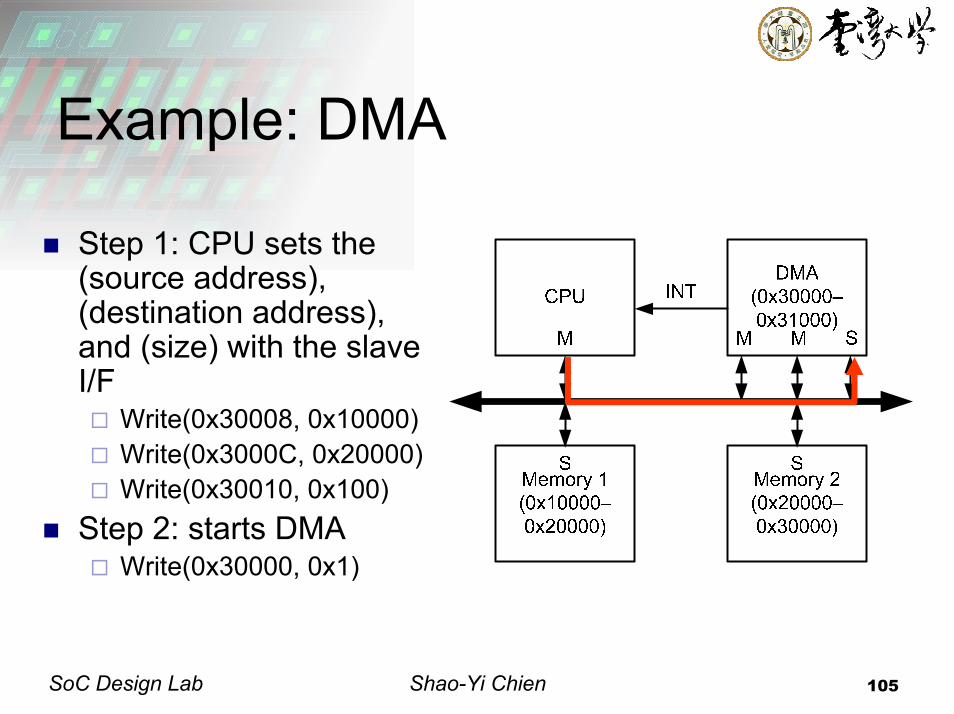
Example: DMA
Step 1: CPU sets the (source address), (destination address), and (size) with the slave I/F
Write(0x30008, 0x10000)Write(0x3000C, 0x20000)Write(0x30010, 0x100)
Step 2: starts DMAWrite(0x30000, 0x1)
Shao-Yi Chien 106SoC Design Lab
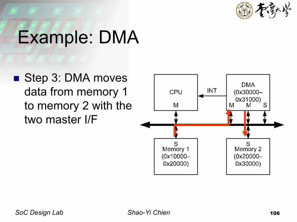
Example: DMA
Step 3: DMA moves data from memory 1 to memory 2 with the two master I/F
Shao-Yi Chien 107SoC Design Lab
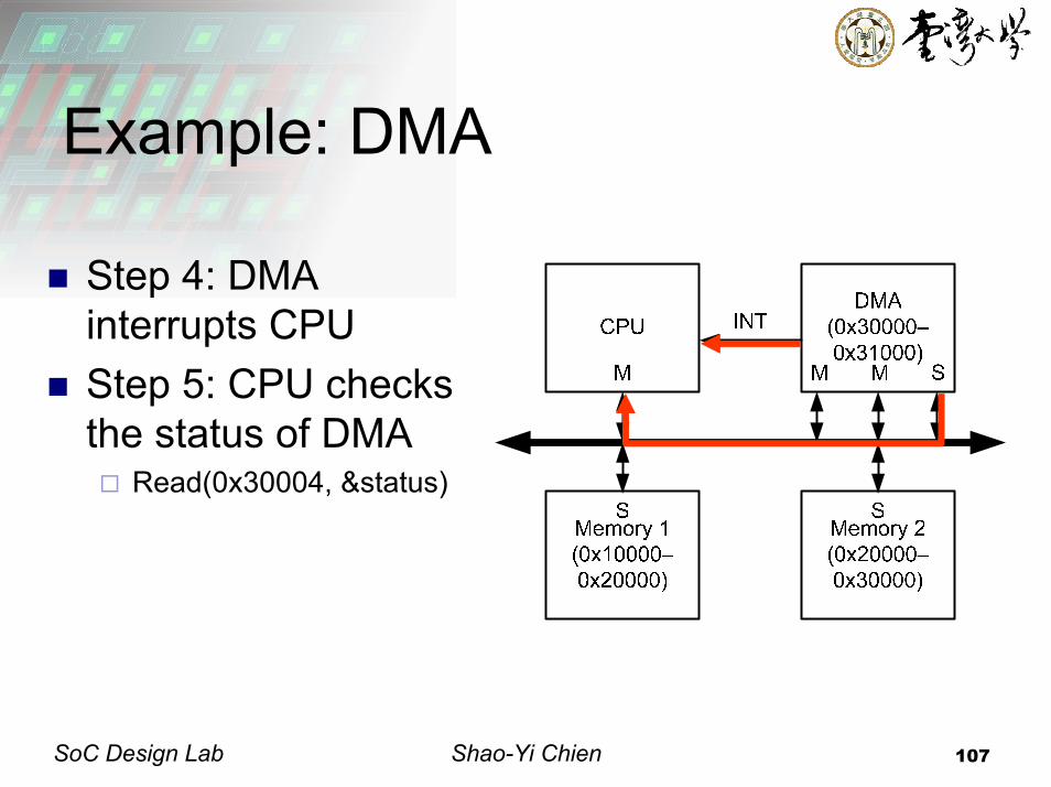
Example: DMA
Step 4: DMA interrupts CPUStep 5: CPU checks the status of DMA
Read(0x30004, &status)