digital logic circuits
DESCRIPTION
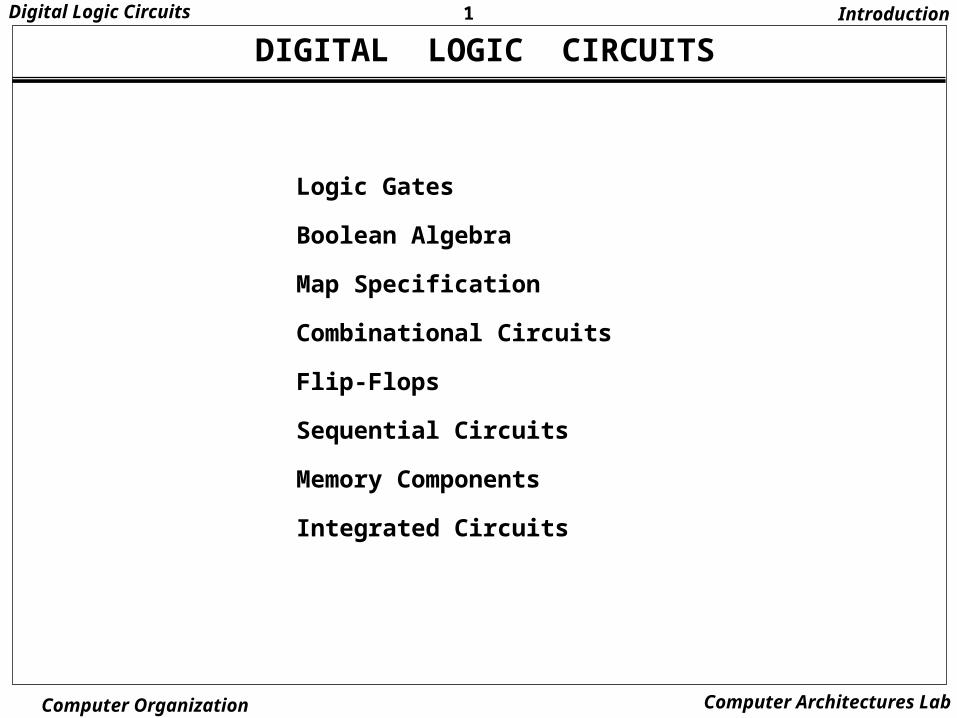
Introduction. DIGITAL LOGIC CIRCUITS. Logic Gates Boolean Algebra Map Specification Combinational Circuits Flip-Flops Sequential Circuits Memory Components Integrated Circuits. Logic Gates. LOGIC GATES. Digital Computers - PowerPoint PPT PresentationTRANSCRIPT
1Digital Logic Circuits
Computer Organization Computer Architectures Lab
Logic Gates
Boolean Algebra
Map Specification
Combinational Circuits
Flip-Flops
Sequential Circuits
Memory Components
Integrated Circuits
DIGITAL LOGIC CIRCUITSIntroduction
1Digital Logic Circuits
Computer Organization Computer Architectures Lab
Logic Gates
LOGIC GATES
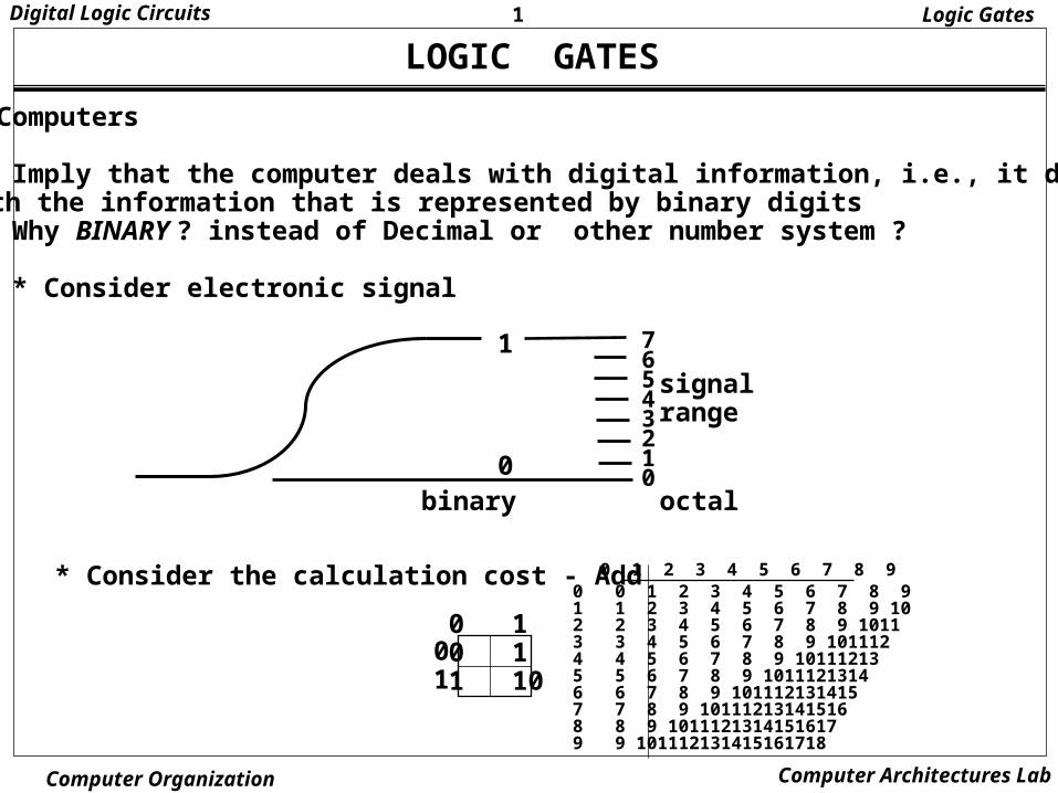
Digital Computers
- Imply that the computer deals with digital information, i.e., it deals with the information that is represented by binary digits
- Why BINARY ? instead of Decimal or other number system ?
* Consider electronic signal
signalrange
0 1 2 3 4 5 6 7 8 90 0 1 2 3 4 5 6 7 8 91 1 2 3 4 5 6 7 8 9 102 2 3 4 5 6 7 8 9 10113 3 4 5 6 7 8 9 1011124 4 5 6 7 8 9 101112135 5 6 7 8 9 10111213146 6 7 8 9 101112131415 7 7 8 9 101112131415168 8 9 10111213141516179 9 101112131415161718
0
1 76543210
binary octal
0 10 11 10
01
* Consider the calculation cost - Add
1Digital Logic Circuits
Computer Organization Computer Architectures Lab
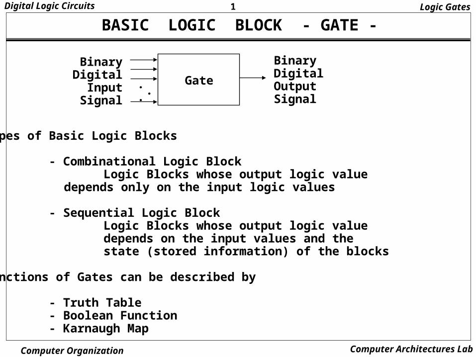
BASIC LOGIC BLOCK - GATE -
Types of Basic Logic Blocks
- Combinational Logic Block Logic Blocks whose output logic value
depends only on the input logic values
- Sequential Logic Block Logic Blocks whose output logic value depends on the input values and the state (stored information) of the blocks
Functions of Gates can be described by
- Truth Table - Boolean Function - Karnaugh Map
Logic Gates
Gate.. .
BinaryDigital
InputSignal
BinaryDigitalOutputSignal
1Digital Logic Circuits
Computer Organization Computer Architectures Lab
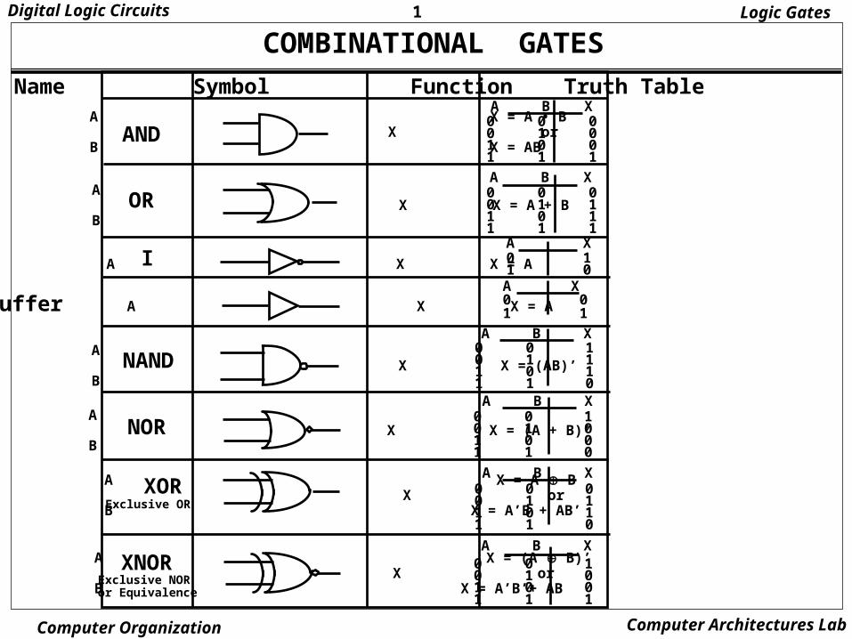
COMBINATIONAL GATES
A X X = (A + B)’B
Name Symbol Function Truth Table
Logic Gates
AND A X = A • B X orB X = AB
0 0 0 0 1 0 1 0 0 1 1 1
0 0 0 0 1 1 1 0 1 1 1 1
OR A X X = A + BB
I A X X = A 0 11 0
Buffer A X X = A A X0 01 1
NANDA X X = (AB)’B
0 0 10 1 11 0 11 1 0
NOR0 0 10 1 01 0 01 1 0
XORExclusive OR
A X = A B X orB X = A’B + AB’
0 0 00 1 11 0 11 1 0
A X = (A B)’ X orB X = A’B’+ AB
0 0 10 1 01 0 01 1 1
XNORExclusive NORor Equivalence
A B X
A B X
A X
A B X
A B X
A B X
A B X
1Digital Logic Circuits
Computer Organization Computer Architectures Lab
BOOLEAN ALGEBRA
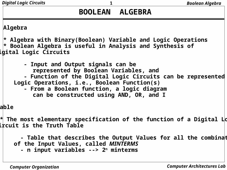
Boolean Algebra
* Algebra with Binary(Boolean) Variable and Logic Operations * Boolean Algebra is useful in Analysis and Synthesis of
Digital Logic Circuits
- Input and Output signals can be represented by Boolean Variables, and - Function of the Digital Logic Circuits can be represented by
Logic Operations, i.e., Boolean Function(s) - From a Boolean function, a logic diagram can be constructed using AND, OR, and I
Truth Table
* The most elementary specification of the function of a Digital Logic Circuit is the Truth Table
- Table that describes the Output Values for all the combinations of the Input Values, called MINTERMS
- n input variables --> 2n minterms
Boolean Algebra
1Digital Logic Circuits
Computer Organization Computer Architectures Lab
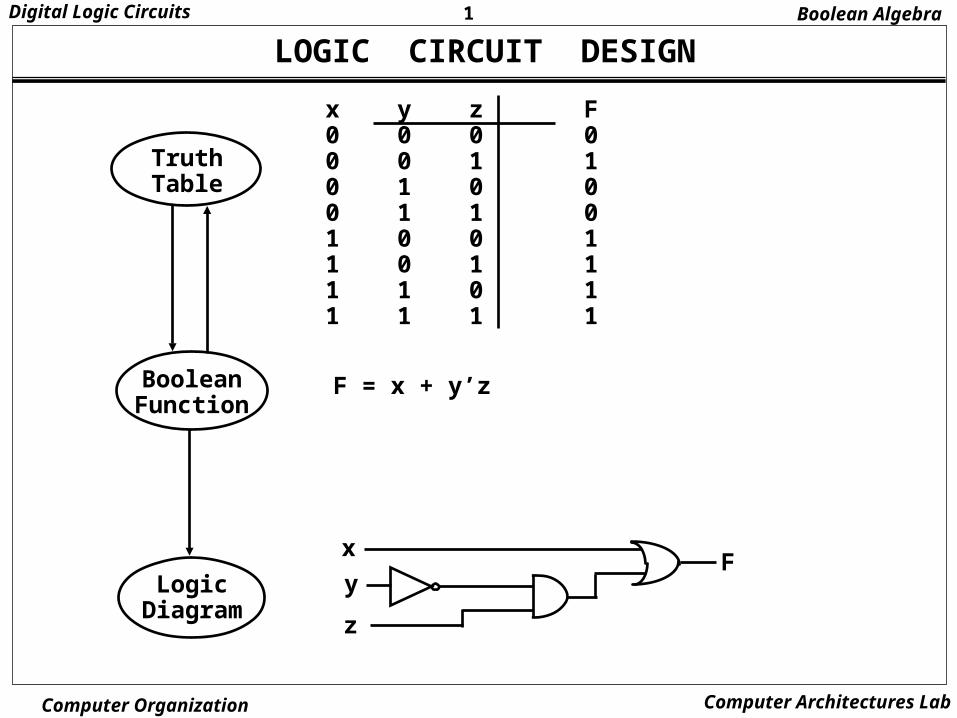
LOGIC CIRCUIT DESIGN
x y z F0 0 0 00 0 1 10 1 0 00 1 1 01 0 0 11 0 1 11 1 0 11 1 1 1
F = x + y’z
Boolean Algebra
x
y
z
F
TruthTable
BooleanFunction
LogicDiagram

1Digital Logic Circuits
Computer Organization Computer Architectures Lab
BASIC IDENTITIES OF BOOLEAN ALGEBRA
[1] x + 0 = x [3] x + 1 = 1[5] x + x = x[7] x + x’ = 1[9] x + y = y + x[11] x + (y + z) = (x + y) + z[13] x(y + z) = xy +xz[15] (x + y)’ = x’y’[17] (x’)’ = x
[2] x • 0 = 0[4] x • 1 = x[6] x • x = x[8] x • X’ = 0[10] xy = yx[12] x(yz) = (xy)z[14] x + yz = (x + y)(x + z)[16] (xy)’ = x’ + y’
[15] and [16] : De Morgan’s TheoremUsefulness of this Table - Simplification of the Boolean function - Derivation of equivalent Boolean functions to obtain logic diagrams utilizing different logic gates -- Ordinarily ANDs, ORs, and Inverters -- But a certain different form of Boolean function may be convenient
to obtain circuits with NANDs or NORs --> Applications of DeMorgans Theorem
x’y’ = (x + y)’ x’+ y’= (xy)’ I, AND --> NOR I, OR --> NAND
Boolean Algebra
1Digital Logic Circuits
Computer Organization Computer Architectures Lab
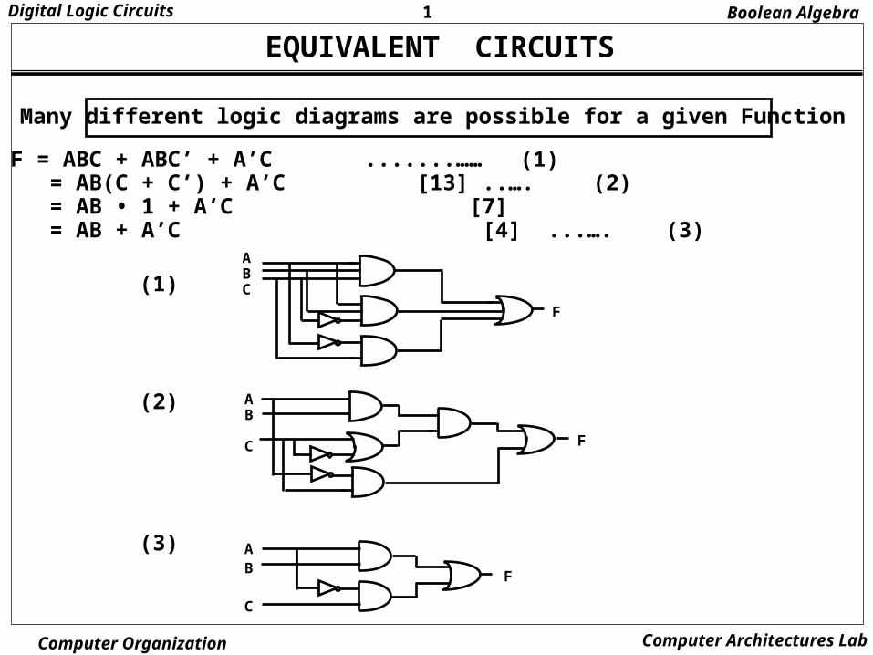
EQUIVALENT CIRCUITS
F = ABC + ABC’ + A’C .......…… (1) = AB(C + C’) + A’C [13] ..…. (2) = AB • 1 + A’C [7] = AB + A’C [4] ...…. (3)
(1)
(2)
(3)
Many different logic diagrams are possible for a given Function
Boolean Algebra
ABC
F
AB
C F
F
AB
C

1Digital Logic Circuits
Computer Organization Computer Architectures Lab
COMPLEMENT OF FUNCTIONS
A Boolean function of a digital logic circuit is represented by only usinglogical variables and AND, OR, and Invert operators.
--> Complement of a Boolean function - Replace all the variables and subexpressions in the parentheses
appearing in the function expression with their respective complements A,B,...,Z,a,b,...,z A’,B’,...,Z’,a’,b’,...,z’ (p + q) (p + q)’ - Replace all the operators with their respective complementary operators
AND OR OR AND
- Basically, extensive applications of the DeMorgan’s theorem
(x1 + x2 + ... + xn )’ x1’x2’... xn’
(x1x2 ... xn)' x1' + x2' +...+ xn'
Boolean Algebra
1Digital Logic Circuits
Computer Organization Computer Architectures Lab
SIMPLIFICATION
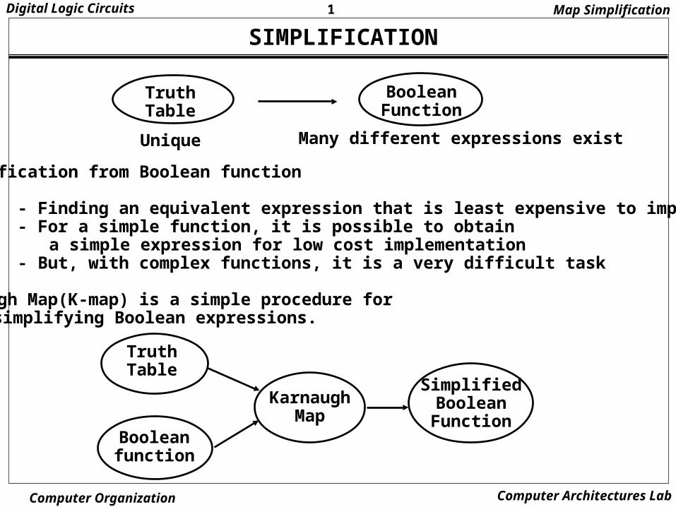
TruthTable
BooleanFunction
Unique Many different expressions exist
Simplification from Boolean function - Finding an equivalent expression that is least expensive to implement - For a simple function, it is possible to obtain a simple expression for low cost implementation - But, with complex functions, it is a very difficult task
Karnaugh Map(K-map) is a simple procedure forsimplifying Boolean expressions.
TruthTable
Booleanfunction
KarnaughMap
SimplifiedBooleanFunction
Map Simplification
1Digital Logic Circuits
Computer Organization Computer Architectures Lab
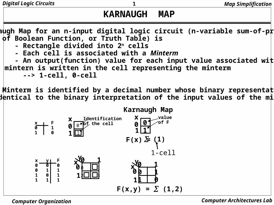
KARNAUGH MAP
Karnaugh Map for an n-input digital logic circuit (n-variable sum-of-products form of Boolean Function, or Truth Table) is - Rectangle divided into 2n cells - Each cell is associated with a Minterm - An output(function) value for each input value associated with a
mintern is written in the cell representing the minterm --> 1-cell, 0-cell
Each Minterm is identified by a decimal number whose binary representation is identical to the binary interpretation of the input values of the minterm.
x F0 11 0
x01
01
x01
0
1
Karnaugh Map valueof F
Identificationof the cell
x y F0 0 00 1 11 0 11 1 1
xy 0 1
01
0 1
2 3
xy 0 1
01
0 11 0
F(x) =
F(x,y) = (1,2)
1-cell
(1)
Map Simplification
1Digital Logic Circuits
Computer Organization Computer Architectures Lab
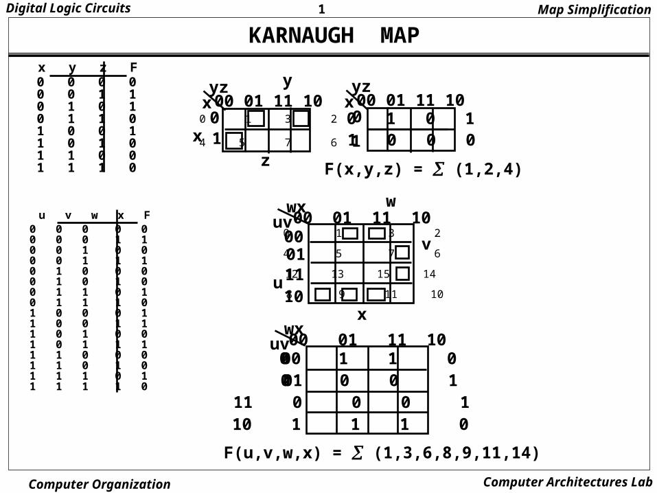
KARNAUGH MAP
0 0 0 00 0 1 10 1 0 10 1 1 01 0 0 11 0 1 01 1 0 01 1 1 0
0 1 0 11 0 0 0
0 0 0 0 00 0 0 1 10 0 1 0 00 0 1 1 10 1 0 0 00 1 0 1 00 1 1 0 10 1 1 1 01 0 0 0 11 0 0 1 11 0 1 0 01 0 1 1 11 1 0 0 01 1 0 1 01 1 1 0 11 1 1 1 0
xyz
00 01 11 100 0 1 3 2
4 5 7 6
xyz
00 01 11 100
1
F(x,y,z) = (1,2,4)
1x
y
z
uvwx
00 01 11 1000011110
0 1 3 2
4 5 7 6
12 13 15 14
8 9 11 10
uvwx
00 01 11 10000111 0 0 0 110 1 1 1 0
0 1 1 00 0 0 1
F(u,v,w,x) = (1,3,6,8,9,11,14)
u
v
w
x
Map Simplification
x y z F
u v w x F
1Digital Logic Circuits
Computer Organization Computer Architectures Lab
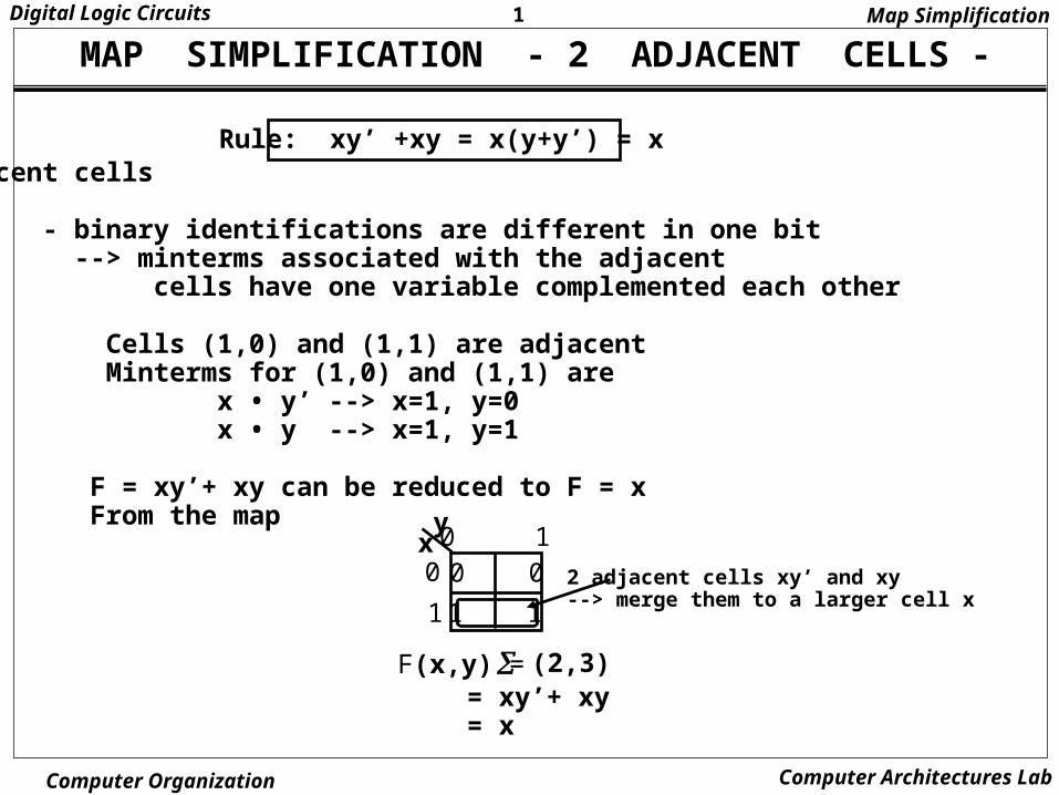
MAP SIMPLIFICATION - 2 ADJACENT CELLS -
Adjacent cells
- binary identifications are different in one bit --> minterms associated with the adjacent cells have one variable complemented each other
Cells (1,0) and (1,1) are adjacent Minterms for (1,0) and (1,1) are x • y’ --> x=1, y=0 x • y --> x=1, y=1 F = xy’+ xy can be reduced to F = x From the map
Rule: xy’ +xy = x(y+y’) = x
xy 0 1
0
1 1 1
0 0
(2,3)F(x,y) =
2 adjacent cells xy’ and xy--> merge them to a larger cell x
= xy’+ xy= x
Map Simplification
1Digital Logic Circuits
Computer Organization Computer Architectures Lab
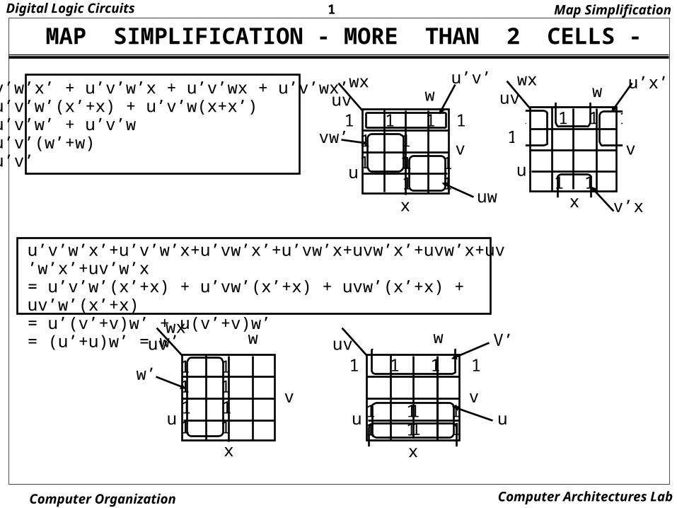
MAP SIMPLIFICATION - MORE THAN 2 CELLS -
u’v’w’x’ + u’v’w’x + u’v’wx + u’v’wx’= u’v’w’(x’+x) + u’v’w(x+x’)= u’v’w’ + u’v’w = u’v’(w’+w) = u’v’
uvwx
1 1 1 1
1 11 1
uvwx
1 1 1 11 1
1 1u
v
w
x
uv
w
x
u’v’
uw
u’x’
v’x
1 11 1
vw’
u’v’w’x’+u’v’w’x+u’vw’x’+u’vw’x+uvw’x’+uvw’x+uv’w’x’+uv’w’x= u’v’w’(x’+x) + u’vw’(x’+x) + uvw’(x’+x) + uv’w’(x’+x)= u’(v’+v)w’ + u(v’+v)w’= (u’+u)w’ = w’
Map Simplification
uv
w
x
uvwx
1 11 11 11 1 u
v
uv
1 11 1
1 11 1
1 1 1 1
x
w’
u
V’w
1Digital Logic Circuits
Computer Organization Computer Architectures Lab
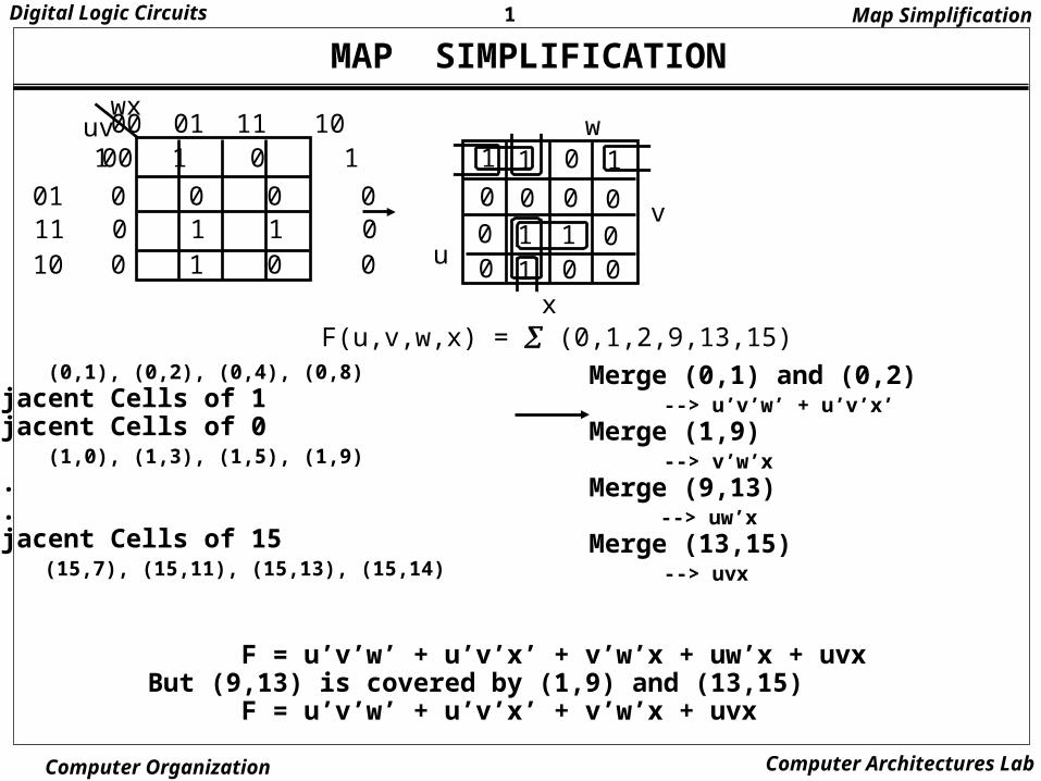
MAP SIMPLIFICATION
(0,1), (0,2), (0,4), (0,8)Adjacent Cells of 1Adjacent Cells of 0 (1,0), (1,3), (1,5), (1,9)......Adjacent Cells of 15 (15,7), (15,11), (15,13), (15,14)
uvwx
00 01 11 1000
01 0 0 0 011 0 1 1 010 0 1 0 0
1 1 0 1
F(u,v,w,x) = (0,1,2,9,13,15)
u
v
w
x
Merge (0,1) and (0,2) --> u’v’w’ + u’v’x’Merge (1,9) --> v’w’xMerge (9,13) --> uw’xMerge (13,15) --> uvx
F = u’v’w’ + u’v’x’ + v’w’x + uw’x + uvxBut (9,13) is covered by (1,9) and (13,15) F = u’v’w’ + u’v’x’ + v’w’x + uvx
Map Simplification
0 0 0 0
1 1 0 1
0 1 1 00 1 0 0
1Digital Logic Circuits
Computer Organization Computer Architectures Lab
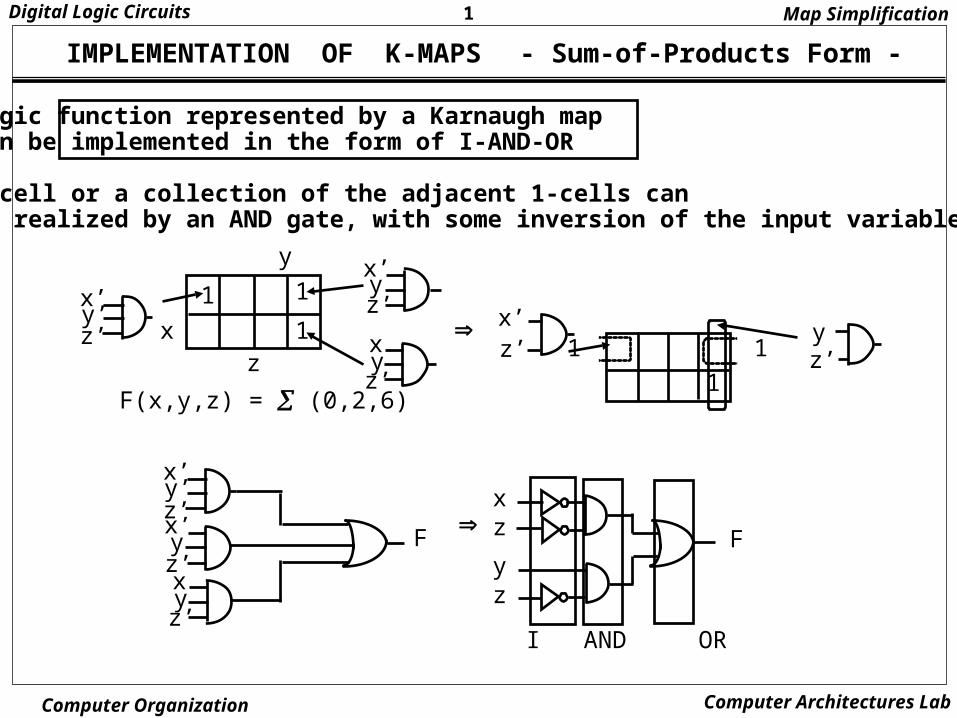
IMPLEMENTATION OF K-MAPS - Sum-of-Products Form -
Logic function represented by a Karnaugh mapcan be implemented in the form of I-AND-OR
A cell or a collection of the adjacent 1-cells canbe realized by an AND gate, with some inversion of the input variables.
x
y
z
x’y’z’
x’yz’
xyz’
1 1
1
F(x,y,z) = (0,2,6)
1 1
1
x’z’
yz’
Map Simplification
x’y
xyz’
x’y’z’
F
xz
yz
F
I AND OR
z’
1Digital Logic Circuits
Computer Organization Computer Architectures Lab
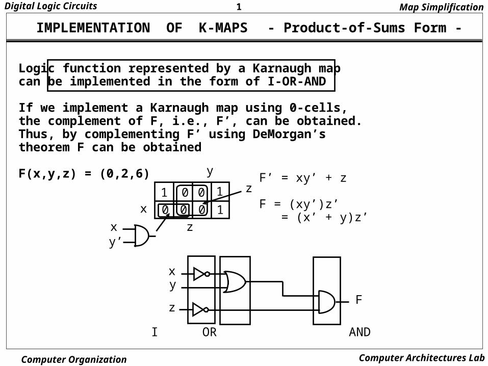
IMPLEMENTATION OF K-MAPS - Product-of-Sums Form -
Logic function represented by a Karnaugh mapcan be implemented in the form of I-OR-AND
If we implement a Karnaugh map using 0-cells,the complement of F, i.e., F’, can be obtained.Thus, by complementing F’ using DeMorgan’stheorem F can be obtained
F(x,y,z) = (0,2,6)
x
y
zxy’
zF’ = xy’ + z
F = (xy’)z’ = (x’ + y)z’
xy
zF
I OR AND
Map Simplification
0 01 1
0 0 0 1
1Digital Logic Circuits
Computer Organization Computer Architectures Lab
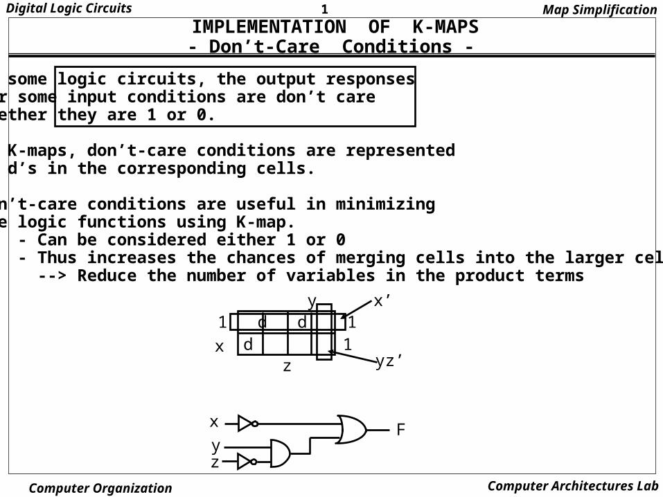
IMPLEMENTATION OF K-MAPS- Don’t-Care Conditions -
In some logic circuits, the output responsesfor some input conditions are don’t care whether they are 1 or 0.
In K-maps, don’t-care conditions are representedby d’s in the corresponding cells.
Don’t-care conditions are useful in minimizingthe logic functions using K-map. - Can be considered either 1 or 0 - Thus increases the chances of merging cells into the larger cells --> Reduce the number of variables in the product terms
x
y
z
1 d d 1d 1
x’
yz’
x
yz
F
Map Simplification
1Digital Logic Circuits
Computer Organization Computer Architectures Lab
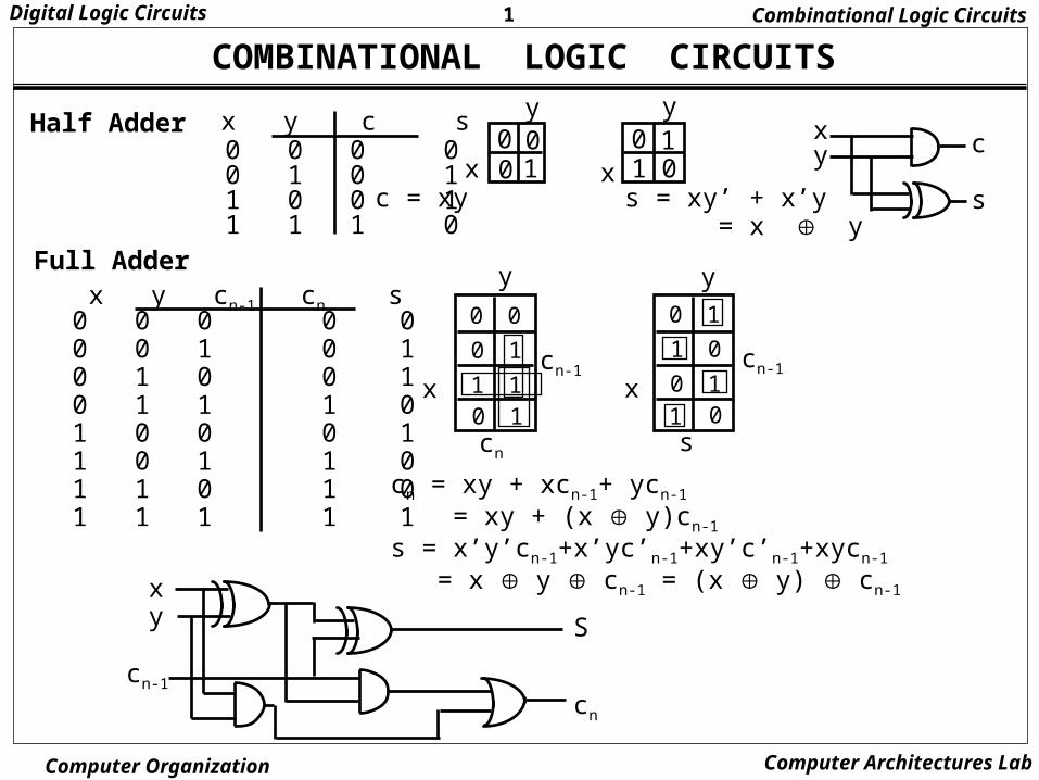
COMBINATIONAL LOGIC CIRCUITS
Half Adder
0 0 0 0 00 0 1 0 10 1 0 0 10 1 1 1 01 0 0 0 11 0 1 1 01 1 0 1 01 1 1 1 1
cn = xy + xcn-1+ ycn-1
= xy + (x y)cn-1 s = x’y’cn-1+x’yc’n-1+xy’c’n-1+xycn-1
= x y cn-1 = (x y) cn-1
x
y
cn-1
x
y
cn-1
cn s
Combinational Logic Circuits
x
y
x
y
c = xy s = xy’ + x’y = x y
xy c
s
xy
cn-1
S
cn
Full Adder
0 0 0 00 1 0 11 0 0 11 1 1 0
x y c s0
10
00
01
1
x y cn-1 cn s0
0
10
0
1
11
0
1
0
1
1
0
10
1Digital Logic Circuits
Computer Organization Computer Architectures Lab
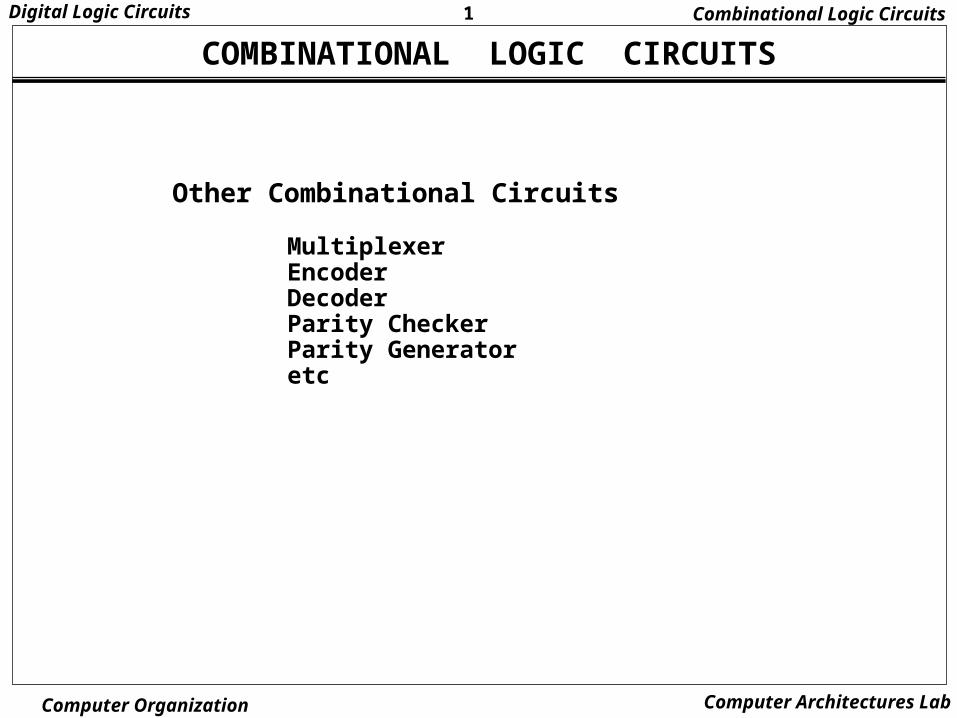
COMBINATIONAL LOGIC CIRCUITS
Other Combinational Circuits
Multiplexer Encoder Decoder Parity Checker Parity Generator etc
Combinational Logic Circuits
1Digital Logic Circuits
Computer Organization Computer Architectures Lab
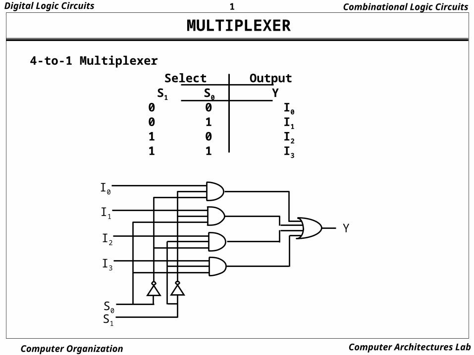
MULTIPLEXERCombinational Logic Circuits
4-to-1 Multiplexer
I0
I1
I2
I3
S0
S1
Y
0 0 I0
0 1 I1
1 0 I2
1 1 I3
Select OutputS1 S0 Y
1Digital Logic Circuits
Computer Organization Computer Architectures Lab
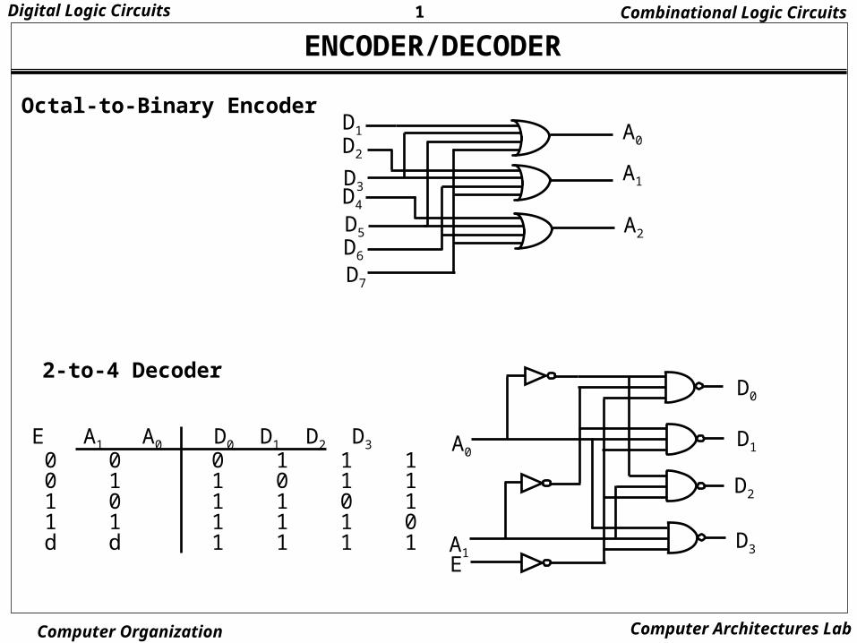
ENCODER/DECODER
Octal-to-Binary Encoder
Combinational Logic Circuits
D1
D2
D3
D5
D6
D7
D4
A0
A1
A2
A0
A1E
D0
D1
D2
D3
0 0 0 0 1 1 10 0 1 1 0 1 10 1 0 1 1 0 10 1 1 1 1 1 01 d d 1 1 1 1
E A1 A0 D0 D1 D2 D3
2-to-4 Decoder
1Digital Logic Circuits
Computer Organization Computer Architectures Lab
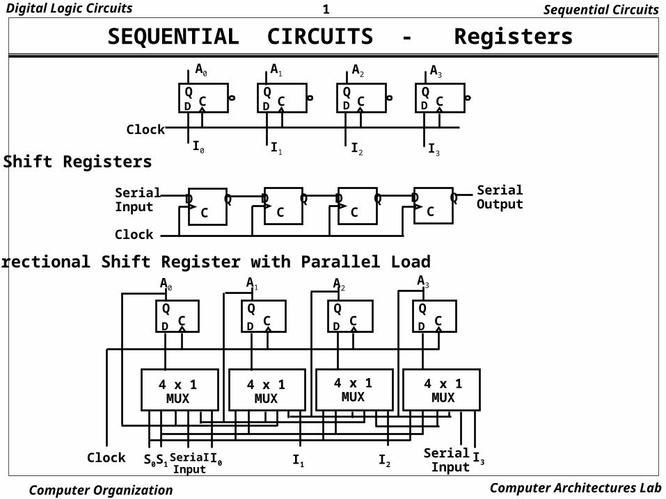
SEQUENTIAL CIRCUITS - Registers
Bidirectional Shift Register with Parallel Load
Sequential Circuits
DQ
C DQ
C DQ
C DQ
C
A0 A1 A2 A3
ClockI0 I1 I2 I3
Shift Registers
D Q C
D Q C
D Q C
D Q C
SerialInput
Clock
SerialOutput
D
QC D
QC D
QC D
QC
A0 A1 A2A3
4 x 1MUX
4 x 1MUX
4 x 1MUX
4 x 1MUX
Clock S0S1SeriaIInput
I0 I1 I2I3
SerialInput
1Digital Logic Circuits
Computer Organization Computer Architectures Lab
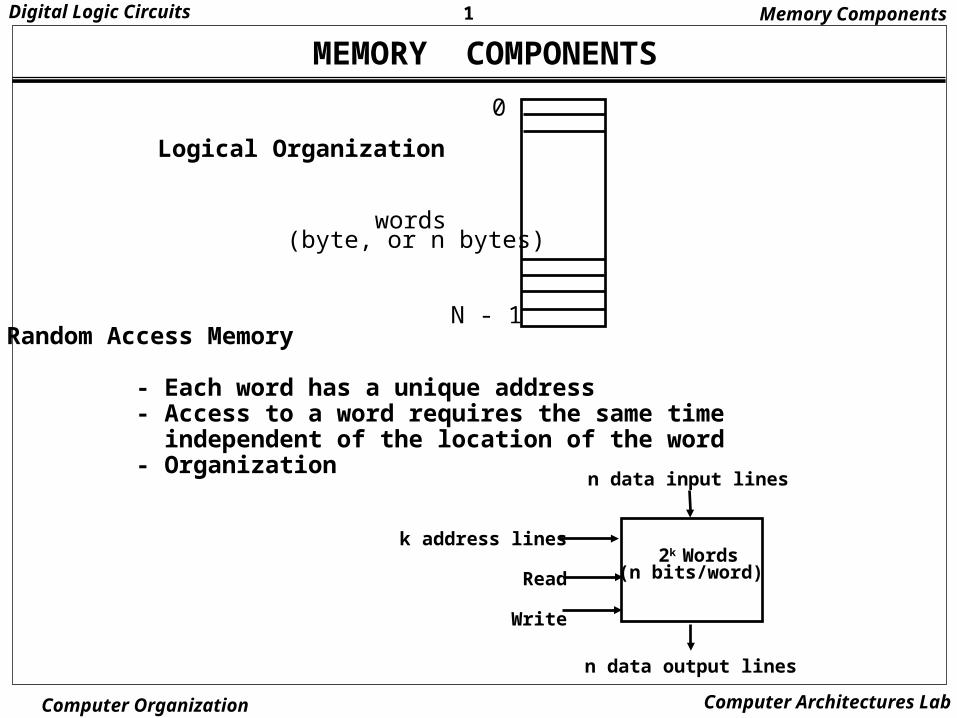
MEMORY COMPONENTS
Logical Organization
Random Access Memory
- Each word has a unique address - Access to a word requires the same time independent of the location of the word - Organization
Memory Components
words(byte, or n bytes)
2k Words(n bits/word)
n data input lines
n data output lines
k address lines
Read
Write
0
N - 1
1Digital Logic Circuits
Computer Organization Computer Architectures Lab
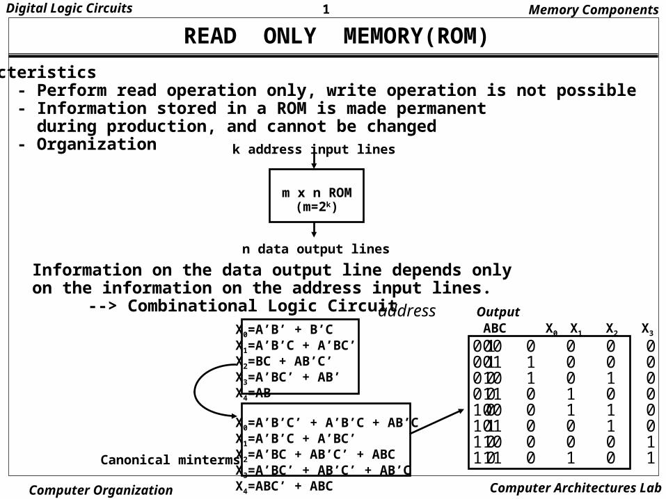
READ ONLY MEMORY(ROM)
Characteristics - Perform read operation only, write operation is not possible - Information stored in a ROM is made permanent during production, and cannot be changed - Organization
Information on the data output line depends only on the information on the address input lines.
--> Combinational Logic Circuit X0=A’B’ + B’CX1=A’B’C + A’BC’X2=BC + AB’C’X3=A’BC’ + AB’X4=AB
X0=A’B’C’ + A’B’C + AB’CX1=A’B’C + A’BC’X2=A’BC + AB’C’ + ABCX3=A’BC’ + AB’C’ + AB’CX4=ABC’ + ABC
Canonical minterms
1 0 0 0 01 1 0 0 00 1 0 1 00 0 1 0 00 0 1 1 01 0 0 1 00 0 0 0 10 0 1 0 1
address Output ABC X0 X1 X2 X3 X4
000001010011100101110111
Memory Components
m x n ROM(m=2k)
k address input lines
n data output lines

1Digital Logic Circuits
Computer Organization Computer Architectures Lab
TYPES OF ROM
ROM- Store information (function) during production- Mask is used in the production process- Unalterable- Low cost for large quantity production --> used in the final products
PROM (Programmable ROM)- Store info electrically using PROM programmer at the user’s site- Unalterable- Higher cost than ROM -> used in the system development phase
-> Can be used in small quantity system
EPROM (Erasable PROM)- Store info electrically using PROM programmer at the user’s site- Stored info is erasable (alterable) using UV light (electrically in
some devices) and rewriteable- Higher cost than PROM but reusable --> used in the system
development phase. Not used in the system production due to erasability
Memory Components
1Digital Logic Circuits
Computer Organization Computer Architectures Lab
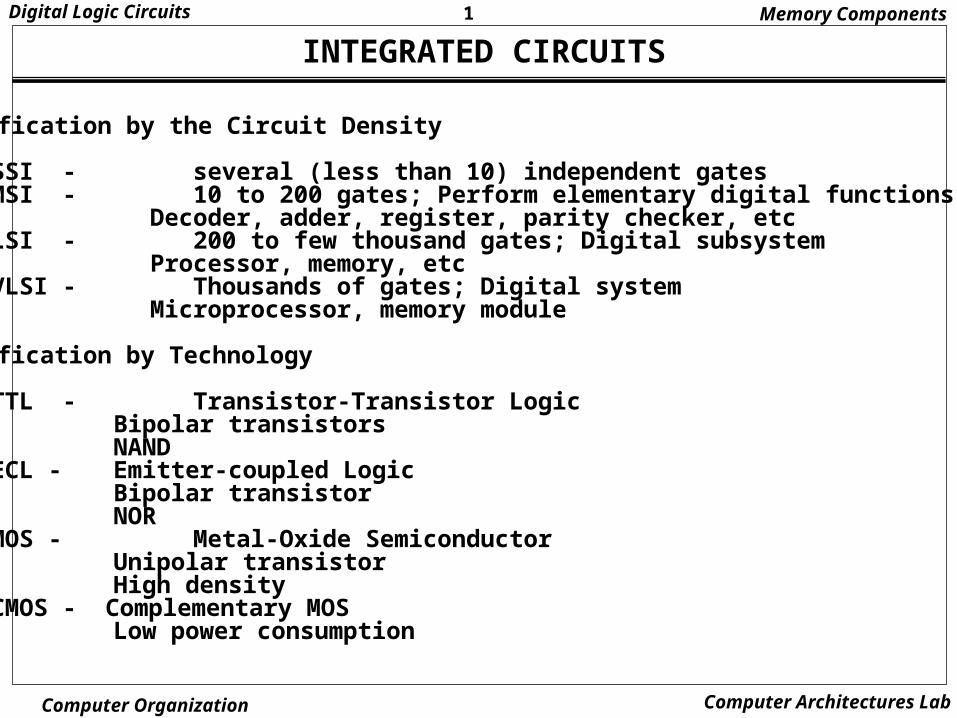
INTEGRATED CIRCUITS
Classification by the Circuit Density
SSI - several (less than 10) independent gatesMSI - 10 to 200 gates; Perform elementary digital functions;
Decoder, adder, register, parity checker, etcLSI - 200 to few thousand gates; Digital subsystem
Processor, memory, etcVLSI - Thousands of gates; Digital system
Microprocessor, memory module
Classification by Technology
TTL - Transistor-Transistor Logic Bipolar transistors NAND
ECL - Emitter-coupled Logic Bipolar transistor NOR
MOS - Metal-Oxide Semiconductor Unipolar transistor High density
CMOS - Complementary MOS Low power consumption
Memory Components