differential high-frequency amplifier with agc … · tl026c differential high-frequency amplifier...
TRANSCRIPT
TL026CDIFFERENTIAL HIGH-FREQUENCY AMPLIFIER WITH AGC
SLFS007A – JUNE 1985 – REVISED JULY 1990
1POST OFFICE BOX 655303 • DALLAS, TEXAS 75265
Low Output Common-Mode Sensitivity toAGC Voltages
Input and Output Impedances Independentof AGC Voltage
Peak Gain . . . 38 dB Typ
Wide AGC Range . . . 50 dB Typ
3-dB Bandwidth . . . 50 MHz
Other Characteristics Similar to NE592 anduA733
description
This device is a monolithic two-stage high-frequency amplifier with differential inputs andoutputs.
Internal feedback provides wide bandwidth, low phase distortion, and excellent gain stability. Variable gainbased on signal summation provides large AGC control over a wide bandwidth with low harmonic distortion.Emitter-follower outputs enable the device to drive capacitive loads. All stages are current-source biased toobtain high common-mode and supply-voltage rejection ratios. The gain may be electronically attenuated byapplying a control voltage to the AGC pin. No external compensation components are required.
This device is particularly useful in TV and radio IF and RF AGC circuits, as well as magnetic-tape and disk-filesystems where AGC is needed. Other applications include video and pulse amplifiers where a large AGC range,wide bandwidth, low phase shift, and excellent gain stability are required.
The TL026C is characterized for operation from 0°C to 70°C.
absolute maximum ratings over operating free-air temperature range (unless otherwise noted) †
Supply voltage, VCC+ (see Note 1) 8 V. . . . . . . . . . . . . . . . . . . . . . . . . . . . . . . . . . . . . . . . . . . . . . . . . . . . . . . . . . . . Supply voltage, VCC– (see Note 1) – 8 V. . . . . . . . . . . . . . . . . . . . . . . . . . . . . . . . . . . . . . . . . . . . . . . . . . . . . . . . . . Differential input voltage ±5 V. . . . . . . . . . . . . . . . . . . . . . . . . . . . . . . . . . . . . . . . . . . . . . . . . . . . . . . . . . . . . . . . . . . . Common-mode input voltage ±6 V. . . . . . . . . . . . . . . . . . . . . . . . . . . . . . . . . . . . . . . . . . . . . . . . . . . . . . . . . . . . . . . . Output current ±10 mA. . . . . . . . . . . . . . . . . . . . . . . . . . . . . . . . . . . . . . . . . . . . . . . . . . . . . . . . . . . . . . . . . . . . . . . . . . Continuous total dissipation See Dissipation Rating Table. . . . . . . . . . . . . . . . . . . . . . . . . . . . . . . . . . . . . . . . . . . Operating free-air temperature range 0°C to 70°C. . . . . . . . . . . . . . . . . . . . . . . . . . . . . . . . . . . . . . . . . . . . . . . . . . Storage temperature range – 65°C to 150°C. . . . . . . . . . . . . . . . . . . . . . . . . . . . . . . . . . . . . . . . . . . . . . . . . . . . . . . Lead temperature range 1,6 mm (1/16 inch) from case for 10 seconds 260°C. . . . . . . . . . . . . . . . . . . . . . . . . .
† Stresses beyond those listed under absolute maximum ratings may cause permanent damage to the device. This is a stress rating only, andfunctional operation of the device at these or any other conditions beyond those indicated in the recommended operating conditions section ofthis specification is not implied. Exposure to absolute-maximum-rated conditions for extended periods may affect device reliability.
NOTE 1: All voltages are with respect to the midpoint of VCC+ and VCC– except differential input and output voltages.
DISSIPATION RATING TABLE
PACKAGETA ≤ 25°C
POWER RATINGOPERATING FACTOR
ABOVE TA = 25°CTA = 70°C
POWER RATING
D 725 mW 5.8 mW/°C 464 mW
P 1000 mW 8.0 mW/°C 640 mW
Copyright 1990, Texas Instruments IncorporatedPRODUCTION DATA information is current as of publication date.Products conform to specifications per the terms of Texas Instrumentsstandard warranty. Production processing does not necessarily includetesting of all parameters.
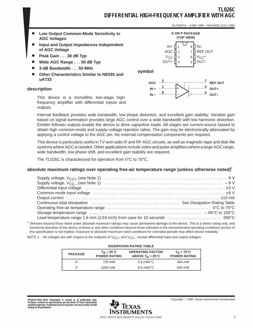
IN–REF OUTVCC+OUT–
1
2
3
4
8
7
6
5
IN+AGCVCC
OUT+
D OR P PACKAGE(TOP VIEW)
symbol
+
–
AGC
IN +
IN –
7
4
5
2
1
8
REF OUT
OUT+
OUT–
TL026CDIFFERENTIAL HIGH-FREQUENCY AMPLIFIER WITH AGC
SLFS007A – JUNE 1985 – REVISED JULY 1990
2 POST OFFICE BOX 655303 • DALLAS, TEXAS 75265
recommended operating conditions
MIN NOM MAX UNIT
Supply voltage, VCC + 3 6 8 V
Supply voltage, VCC – – 3 – 6 – 8 V
Operating free-air temperature range, TA 0 70 °C
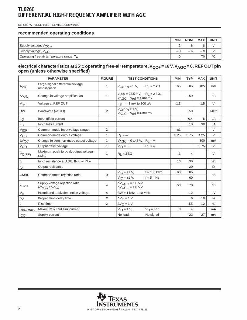
electrical characteristics at 25 °C operating free-air temperature, V CC+ = ±6 V, VAGC = 0, REF OUT pinopen (unless otherwise specified)
PARAMETER FIGURE TEST CONDITIONS MIN TYP MAX UNIT
AVDLarge-signal differential voltageamplification
1 VO(PP) = 3 V, RL = 2 kΩ 65 85 105 V/V
∆AVD Change in voltage amplification 1VIPP = 28.5 mV, RL = 2 kΩ,VAGC – Vref = ±180 mV
– 50 dB
Vref Voltage at REF OUT Iref = – 1 mA to 100 µA 1.3 1.5 V
BW Bandwidth (–3 dB) 2VO(PP) = 1 V,VAGC – Vref = ±180 mV
50 MHz
IIO Input offset current 0.4 5 µA
IIB Input bias current 10 30 µA
VICR Common-mode input voltage range 3 ±1 V
VOC Common-mode output voltage 1 RL = ∞ 3.25 3.75 4.25 V
∆VOC Change in common-mode output voltage 1 VAGC = 0 to 2 V, RL = ∞ 300 mV
VOO Output offset voltage 1 VID = 0, RL = ∞ 0.75 V
VO(PP)Maximum peak-to-peak output voltageswing
1 RL = 2 kΩ 3 4 V
ri Input resistance at AGC, IN+, or IN – 10 30 kΩ
ro Output resistance 20 Ω
CMRR Common mode rejection ratio 3VIC = ±1 V, f = 100 kHz 60 86
dBCMRR Common-mode rejection ratio 3VIC = ±1 V, f = 5 mHz 60
dB
kSVRSupply voltage rejection ratio(∆VCC / ∆VIO)
4∆VCC + = ± 0.5 V,∆VCC – = ± 0.5 V
50 70 dB
Vn Broadband equivalent noise voltage 4 BW = 1 kHz to 10 MHz 12 µV
tpd Propagation delay time 2 ∆VO = 1 V 6 10 ns
tr Rise time 2 ∆VO = 1 V 4.5 12 ns
Isink(max) Maximum output sink current VID = 1 V, VO = 3 V 3 4 mA
ICC Supply current No load, No signal 22 27 mA
TL026CDIFFERENTIAL HIGH-FREQUENCY AMPLIFIER WITH AGC
SLFS007A – JUNE 1985 – REVISED JULY 1990
3POST OFFICE BOX 655303 • DALLAS, TEXAS 75265
electrical characteristics over recommended operating free-air temperature range, V CC± = ±6 V,VAGC = 0, REF OUT pin open (unless otherwise specified)
PARAMETER FIGURE TEST CONDITIONS MIN TYP MAX UNIT
AVD Large-signal differential voltage amplification 1 VO(PP) = 3 V, RL = 2 kΩ 55 115 V/V
IIO Input offset current 6 µA
IIB Input bias current 40 µA
VICR Common-mode input voltage range 3 ±1 V
VOO Output offset voltage 1 VID = 0, RL = ∞ 1.5 V
VO(PP) Maximum peak-to-peak output voltage swing 1 RL = 2 kΩ 2.8 V
ri Input resistance at AGC, IN+, or IN – 8 kΩ
CMRR Common-mode rejection ratio 3 VIC = ±1 V, f = 100 kHz 50 dB
kSVRSupply voltage rejection ratio(∆VCC / ∆VIO)
4∆VCC + = ± 0.5 V,∆VCC – = ± 0.5 V
50 dB
Isink(max) Maximum output sink current VID = 1 V, VO = 3 V 2.8 4 mA
ICC Supply current 1 No load, No signal 30 mA
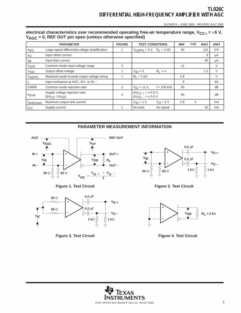
PARAMETER MEASUREMENT INFORMATION
IN +
IN –
AGC
OUT +
OUT –
REF OUT
RL
50 Ω 50 ΩVOC
VO VO 2
+
–
VAGC Vref
VID VOD
Figure 1. Test Circuit
1 kΩ1 kΩ
VO +
VO –
50 Ω 50 Ω
+
–
VID
0.2 µF
0.2 µF
Figure 2. Test Circuit
1 kΩ1 kΩ
VO +
VO –
50 Ω
50 Ω
+
–
0.2 µF
0.2 µF
VIC
Figure 3. Test Circuit
RL = 2 kΩ
+
–
VOD
Figure 4. Test Circuit
TL026CDIFFERENTIAL HIGH-FREQUENCY AMPLIFIER WITH AGC
SLFS007A – JUNE 1985 – REVISED JULY 1990
4 POST OFFICE BOX 655303 • DALLAS, TEXAS 75265
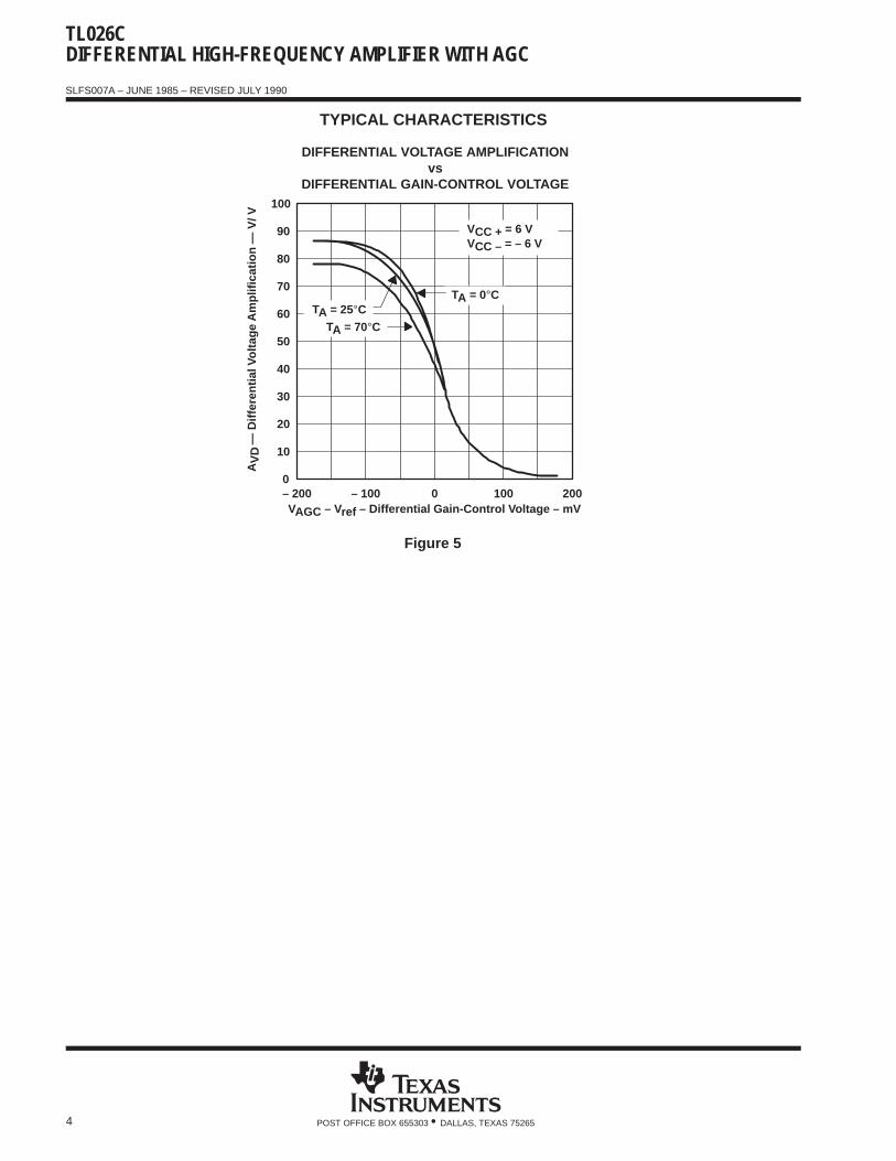
TYPICAL CHARACTERISTICS
Figure 5
– 200 – 100 0 100 200
A
DIFFERENTIAL VOLTAGE AMPLIFICATIONvs
DIFFERENTIAL GAIN-CONTROL VOLTAGE
VD
VAGC – Vref – Differential Gain-Control Voltage – mV
100
90
80
70
60
50
40
30
20
10
0
VCC + = 6 VVCC – = – 6 V
TA = 0°C
TA = 70°CTA = 25°C
— D
iffer
entia
l Vol
tage
Am
plifi
catio
n—
V/V
TL026CDIFFERENTIAL HIGH-FREQUENCY AMPLIFIER WITH AGC
SLFS007A – JUNE 1985 – REVISED JULY 1990
5POST OFFICE BOX 655303 • DALLAS, TEXAS 75265
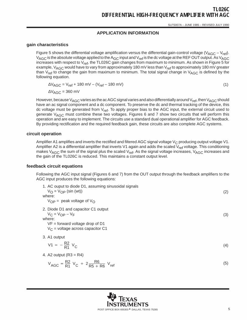
APPLICATION INFORMATION
gain characteristics
Figure 5 shows the differential voltage amplification versus the differential gain-control voltage (VAGC – Vref).VAGC is the absolute voltage applied to the AGC input and Vref is the dc voltage at the REF OUT output. As VAGCincreases with respect to Vref, the TL026C gain changes from maximum to minimum. As shown in Figure 5 forexample, VAGC would have to vary from approximately 180 mV less than Vref to approximately 180 mV greaterthan Vref to change the gain from maximum to minimum. The total signal change in VAGC is defined by thefollowing equation.
∆VAGC = Vref + 180 mV – (Vref – 180 mV)
∆VAGC = 360 mV
(1)
However, because VAGC varies as the ac AGC signal varies and also differentially around Vref, then VAGC shouldhave an ac signal component and a dc component. To preserve the dc and thermal tracking of the device, thisdc voltage must be generated from Vref. To apply proper bias to the AGC input, the external circuit used togenerate VAGC must combine these two voltages. Figures 6 and 7 show two circuits that will perform thisoperation and are easy to implement. The circuits use a standard dual operational amplifier for AGC feedback.By providing rectification and the required feedback gain, these circuits are also complete AGC systems.
circuit operation
Amplifier A1 amplifies and inverts the rectified and filtered AGC signal voltage VC producing output voltage V1.Amplifier A2 is a differential amplifier that inverts V1 again and adds the scaled Vref voltage. This conditioningmakes VAGC the sum of the signal plus the scaled Vref. As the signal voltage increases, VAGC increases andthe gain of the TL026C is reduced. This maintains a constant output level.
feedback circuit equations
Following the AGC input signal (Figures 6 and 7) from the OUT output through the feedback amplifiers to theAGC input produces the following equations:
(2)1. AC ouput to diode D1, assuming sinusoidal signals
VO = VOP (sin (wt))where:
VOP = peak voltage of VO
(3)2. Diode D1 and capacitor C1 output
VC = VOP – VFwhere:
VF = forward voltage drop of D1VC = voltage across capacitor C1
(4)
3. A1 output
V1R2R1
VC
(5)
4. A2 output (R3 = R4)
VAGCR2R1
VC 2 R6R5R6
Vref
TL026CDIFFERENTIAL HIGH-FREQUENCY AMPLIFIER WITH AGC
SLFS007A – JUNE 1985 – REVISED JULY 1990
6 POST OFFICE BOX 655303 • DALLAS, TEXAS 75265
APPLICATION INFORMATION
Amplifier A2 inverts V1 producing a positive AGC signal voltage. Therefore, the input voltage to the TL026CAGC pin consists of an AGC signal equal to:
(6)R2R1
VC
and a dc voltage derived from Vref, defined as the quiescent value of VAGC.
VAGC(q) 2 R6R5R6
Vref (7)
For the initial resistor calculations, Vref is assumed to be typically 1.4 V making quiescent VAGC approximately1.22 V (VAGC(q) = Vref – 180 mV). This voltage allows the TL026C to operate at maximum gain under no-signaland low-signal conditions. In addition, with Vref used as both internal and external reference, its variation fromdevice to device automatically adjusts the overall bias and makes AGC operation essentially independent ofthe absolute value of Vref. The resistor divider needs to be calculated only once and is valid for the full toleranceof Vref.
output voltage limits (see Figures 6 and 7)
The output voltage level desired must fall within the following limits:
1. Because the data sheet minimum output swing is 3 V peak-to-peak using a 2-kΩ load resistor, theuser-selected design limit for the peak output swing should not exceed 1.5 V.
2. The voltage drop of the rectifying diode determines the lower voltage limit. When a silicon diode isused, this voltage is approximately 0.7 V. The output voltage VO must have sufficient amplitude toexceed the rectifying diode drop. Aschottky diode can be used to reduce the VO level required.
gain calculations for a peak output voltage of 1 V
A peak output voltage of 1 V was chosen for gain calculations because it is approximately midway between thelimits of conditions 1 and 2 in the preceding paragraph.
Using equation 3 (VC = VOP – Vd), VC is calculated as follows:
VC = 1 V – 0.7 V
VC = 0.3 V
Therefore, the gain of A1 must produce a voltage V1 that is equal to or greater than the total change in VAGCfor maximum TL026C gain change.
With a total change in VAGC of 360 mV and using equation 4, the calculation is as follows:
V1VC
VAGCVC
R2R1
0.360.3
1.2
If R1 is 10 kΩ, R2 is 1.2 time R1 or 12 kΩ.
Since the output voltage for this circuit must be between 0.85 V and 1.3 V, the component values inFigures 6 and 7 provide a nominal 1-V peak output limit. This limit is the best choice to allow for temperaturevariations of the diode and minimum output voltage specification.
TL026CDIFFERENTIAL HIGH-FREQUENCY AMPLIFIER WITH AGC
SLFS007A – JUNE 1985 – REVISED JULY 1990
7POST OFFICE BOX 655303 • DALLAS, TEXAS 75265
APPLICATION INFORMATION
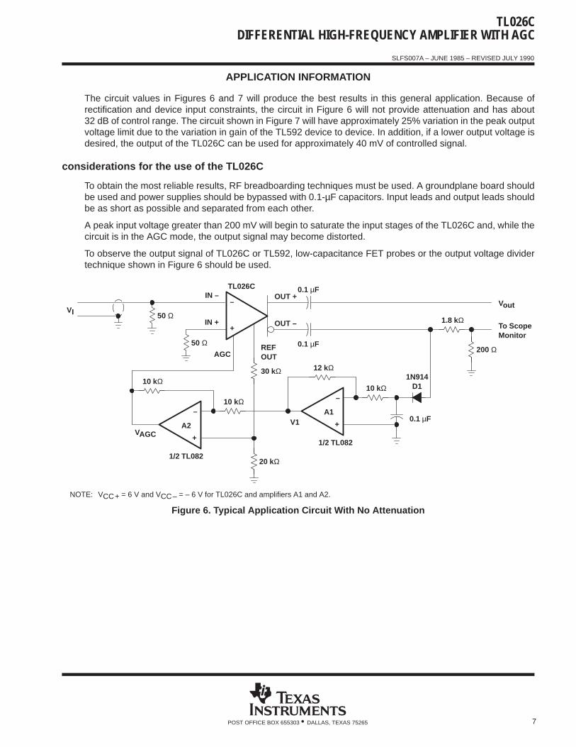
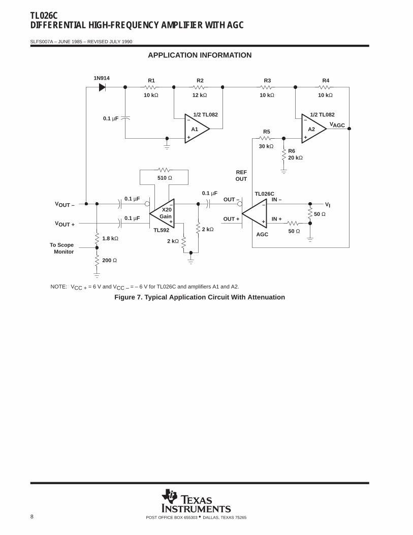
The circuit values in Figures 6 and 7 will produce the best results in this general application. Because ofrectification and device input constraints, the circuit in Figure 6 will not provide attenuation and has about32 dB of control range. The circuit shown in Figure 7 will have approximately 25% variation in the peak outputvoltage limit due to the variation in gain of the TL592 device to device. In addition, if a lower output voltage isdesired, the output of the TL026C can be used for approximately 40 mV of controlled signal.
considerations for the use of the TL026C
To obtain the most reliable results, RF breadboarding techniques must be used. A groundplane board shouldbe used and power supplies should be bypassed with 0.1-µF capacitors. Input leads and output leads shouldbe as short as possible and separated from each other.
A peak input voltage greater than 200 mV will begin to saturate the input stages of the TL026C and, while thecircuit is in the AGC mode, the output signal may become distorted.
To observe the output signal of TL026C or TL592, low-capacitance FET probes or the output voltage dividertechnique shown in Figure 6 should be used.
–
+
+
–
OUT +
OUT –
0.1 µF
0.1 µFREFOUT
30 kΩ
To ScopeMonitor
Vout
200 Ω
1.8 kΩ
IN –
IN +
50 ΩAGC
10 kΩ
10 kΩ
VAGCA2
20 kΩ
50 ΩVI
+
–10 kΩ
A1
12 kΩ1N914
D1
0.1 µFV1
1/2 TL082
1/2 TL082
TL026C
NOTE: VCC+ = 6 V and VCC– = – 6 V for TL026C and amplifiers A1 and A2.
Figure 6. Typical Application Circuit With No Attenuation
TL026CDIFFERENTIAL HIGH-FREQUENCY AMPLIFIER WITH AGC
SLFS007A – JUNE 1985 – REVISED JULY 1990
8 POST OFFICE BOX 655303 • DALLAS, TEXAS 75265
APPLICATION INFORMATION
–
+
R620 kΩ
50 Ω
0.1 µF
VOUT –
VOUT +
0.1 µF
A1
50 Ω
10 kΩ
R1
12 kΩ
R2
1/2 TL0820.1 µF
OUT –
OUT +
IN –
IN +
AGC
To ScopeMonitor
–
+
A2
10 kΩ
R4
1/2 TL082
30 kΩ
R5
10 kΩ
R3
VAGC
VI
1.8 kΩ
200 Ω
1N914
REFOUT
TL026C0.1 µF
TL592 2 kΩ
2 kΩ
510 Ω
+
–
+
–X20
Gain
NOTE: VCC + = 6 V and VCC – = – 6 V for TL026C and amplifiers A1 and A2.
Figure 7. Typical Application Circuit With Attenuation
PACKAGE OPTION ADDENDUM
www.ti.com 17-Mar-2017
Addendum-Page 1
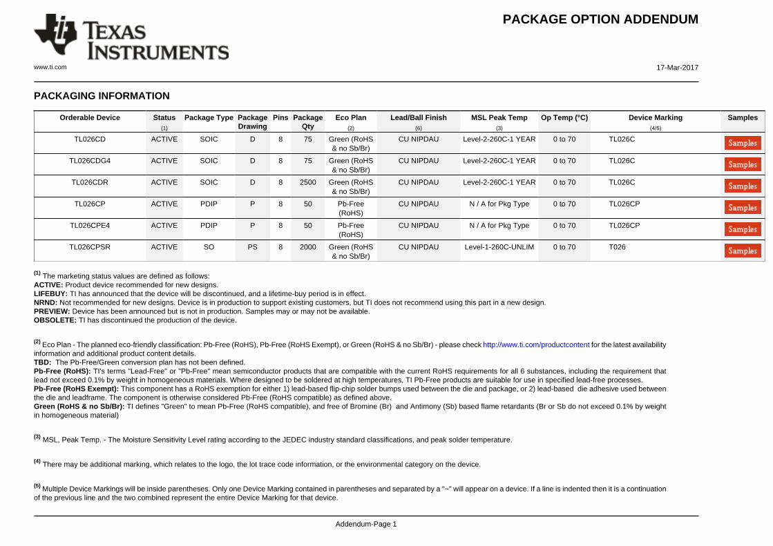
PACKAGING INFORMATION
Orderable Device Status(1)
Package Type PackageDrawing
Pins PackageQty
Eco Plan(2)
Lead/Ball Finish(6)
MSL Peak Temp(3)
Op Temp (°C) Device Marking(4/5)
Samples
TL026CD ACTIVE SOIC D 8 75 Green (RoHS& no Sb/Br)
CU NIPDAU Level-2-260C-1 YEAR 0 to 70 TL026C
TL026CDG4 ACTIVE SOIC D 8 75 Green (RoHS& no Sb/Br)
CU NIPDAU Level-2-260C-1 YEAR 0 to 70 TL026C
TL026CDR ACTIVE SOIC D 8 2500 Green (RoHS& no Sb/Br)
CU NIPDAU Level-2-260C-1 YEAR 0 to 70 TL026C
TL026CP ACTIVE PDIP P 8 50 Pb-Free(RoHS)
CU NIPDAU N / A for Pkg Type 0 to 70 TL026CP
TL026CPE4 ACTIVE PDIP P 8 50 Pb-Free(RoHS)
CU NIPDAU N / A for Pkg Type 0 to 70 TL026CP
TL026CPSR ACTIVE SO PS 8 2000 Green (RoHS& no Sb/Br)
CU NIPDAU Level-1-260C-UNLIM 0 to 70 T026
(1) The marketing status values are defined as follows:ACTIVE: Product device recommended for new designs.LIFEBUY: TI has announced that the device will be discontinued, and a lifetime-buy period is in effect.NRND: Not recommended for new designs. Device is in production to support existing customers, but TI does not recommend using this part in a new design.PREVIEW: Device has been announced but is not in production. Samples may or may not be available.OBSOLETE: TI has discontinued the production of the device.
(2) Eco Plan - The planned eco-friendly classification: Pb-Free (RoHS), Pb-Free (RoHS Exempt), or Green (RoHS & no Sb/Br) - please check http://www.ti.com/productcontent for the latest availabilityinformation and additional product content details.TBD: The Pb-Free/Green conversion plan has not been defined.Pb-Free (RoHS): TI's terms "Lead-Free" or "Pb-Free" mean semiconductor products that are compatible with the current RoHS requirements for all 6 substances, including the requirement thatlead not exceed 0.1% by weight in homogeneous materials. Where designed to be soldered at high temperatures, TI Pb-Free products are suitable for use in specified lead-free processes.Pb-Free (RoHS Exempt): This component has a RoHS exemption for either 1) lead-based flip-chip solder bumps used between the die and package, or 2) lead-based die adhesive used betweenthe die and leadframe. The component is otherwise considered Pb-Free (RoHS compatible) as defined above.Green (RoHS & no Sb/Br): TI defines "Green" to mean Pb-Free (RoHS compatible), and free of Bromine (Br) and Antimony (Sb) based flame retardants (Br or Sb do not exceed 0.1% by weightin homogeneous material)
(3) MSL, Peak Temp. - The Moisture Sensitivity Level rating according to the JEDEC industry standard classifications, and peak solder temperature.
(4) There may be additional marking, which relates to the logo, the lot trace code information, or the environmental category on the device.
(5) Multiple Device Markings will be inside parentheses. Only one Device Marking contained in parentheses and separated by a "~" will appear on a device. If a line is indented then it is a continuationof the previous line and the two combined represent the entire Device Marking for that device.
PACKAGE OPTION ADDENDUM
www.ti.com 17-Mar-2017
Addendum-Page 2
(6) Lead/Ball Finish - Orderable Devices may have multiple material finish options. Finish options are separated by a vertical ruled line. Lead/Ball Finish values may wrap to two lines if the finishvalue exceeds the maximum column width.
Important Information and Disclaimer:The information provided on this page represents TI's knowledge and belief as of the date that it is provided. TI bases its knowledge and belief on informationprovided by third parties, and makes no representation or warranty as to the accuracy of such information. Efforts are underway to better integrate information from third parties. TI has taken andcontinues to take reasonable steps to provide representative and accurate information but may not have conducted destructive testing or chemical analysis on incoming materials and chemicals.TI and TI suppliers consider certain information to be proprietary, and thus CAS numbers and other limited information may not be available for release.
In no event shall TI's liability arising out of such information exceed the total purchase price of the TI part(s) at issue in this document sold by TI to Customer on an annual basis.
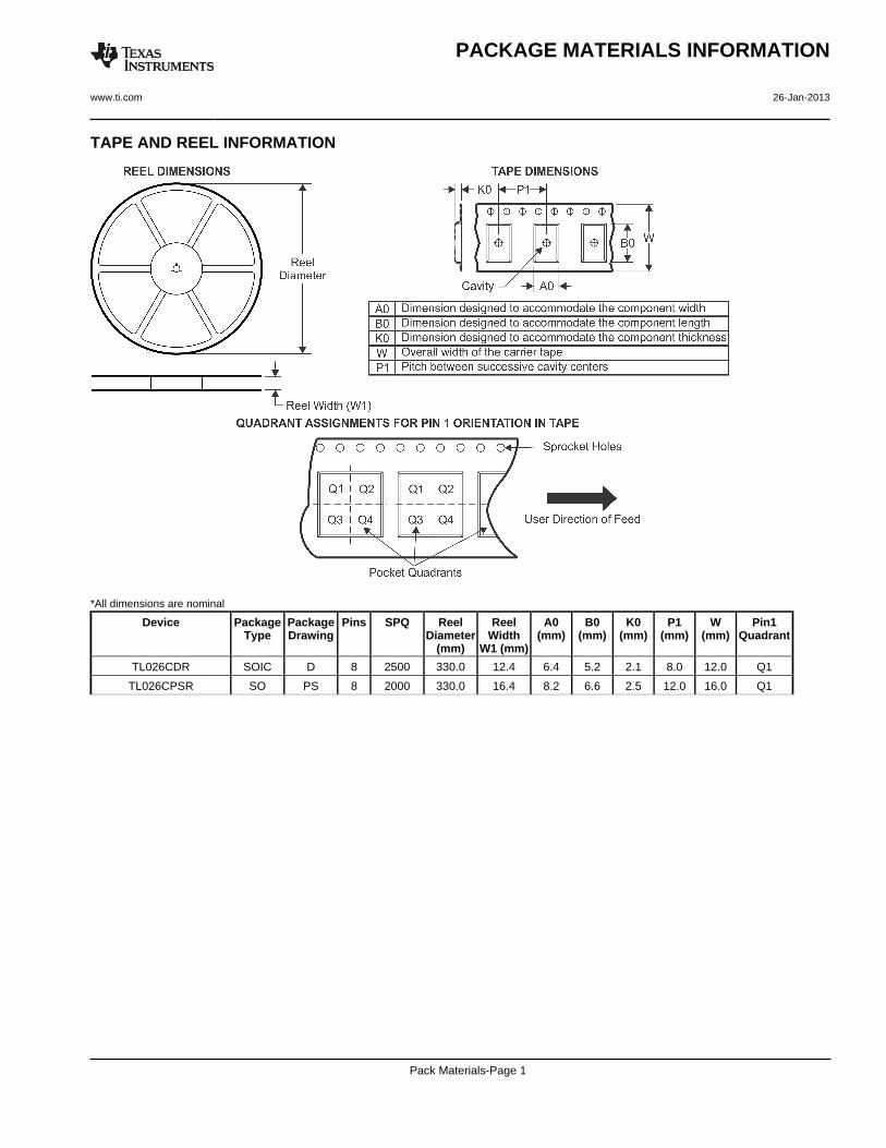
TAPE AND REEL INFORMATION
*All dimensions are nominal
Device PackageType
PackageDrawing
Pins SPQ ReelDiameter
(mm)
ReelWidth
W1 (mm)
A0(mm)
B0(mm)
K0(mm)
P1(mm)
W(mm)
Pin1Quadrant
TL026CDR SOIC D 8 2500 330.0 12.4 6.4 5.2 2.1 8.0 12.0 Q1
TL026CPSR SO PS 8 2000 330.0 16.4 8.2 6.6 2.5 12.0 16.0 Q1
PACKAGE MATERIALS INFORMATION
www.ti.com 26-Jan-2013
Pack Materials-Page 1
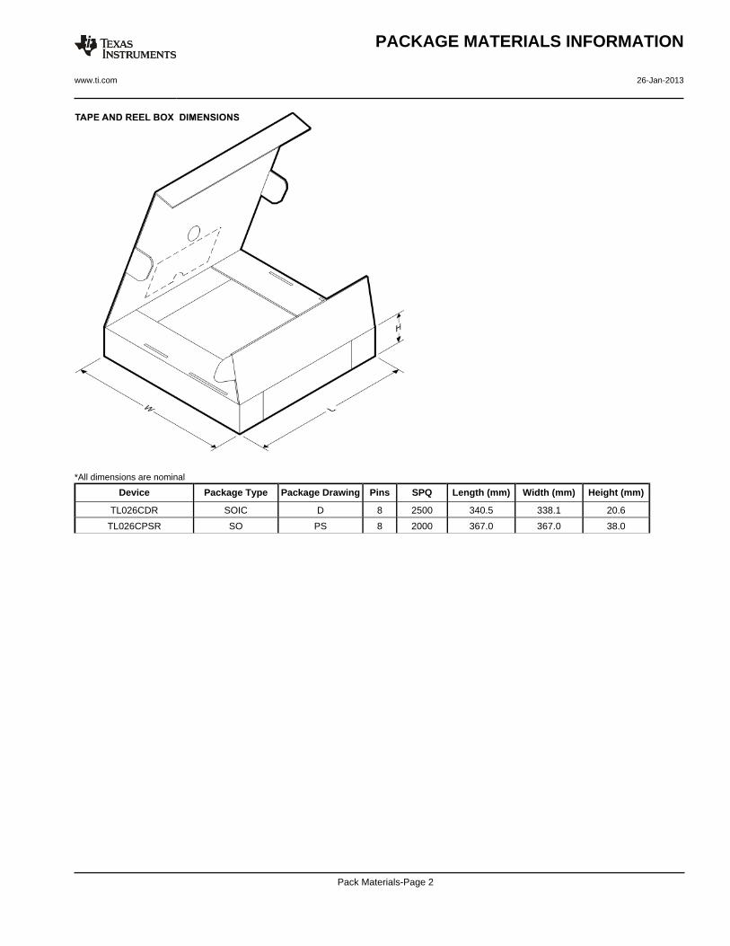
*All dimensions are nominal
Device Package Type Package Drawing Pins SPQ Length (mm) Width (mm) Height (mm)
TL026CDR SOIC D 8 2500 340.5 338.1 20.6
TL026CPSR SO PS 8 2000 367.0 367.0 38.0
PACKAGE MATERIALS INFORMATION
www.ti.com 26-Jan-2013
Pack Materials-Page 2
IMPORTANT NOTICE
Texas Instruments Incorporated (TI) reserves the right to make corrections, enhancements, improvements and other changes to itssemiconductor products and services per JESD46, latest issue, and to discontinue any product or service per JESD48, latest issue. Buyersshould obtain the latest relevant information before placing orders and should verify that such information is current and complete.TI’s published terms of sale for semiconductor products (http://www.ti.com/sc/docs/stdterms.htm) apply to the sale of packaged integratedcircuit products that TI has qualified and released to market. Additional terms may apply to the use or sale of other types of TI products andservices.Reproduction of significant portions of TI information in TI data sheets is permissible only if reproduction is without alteration and isaccompanied by all associated warranties, conditions, limitations, and notices. TI is not responsible or liable for such reproduceddocumentation. Information of third parties may be subject to additional restrictions. Resale of TI products or services with statementsdifferent from or beyond the parameters stated by TI for that product or service voids all express and any implied warranties for theassociated TI product or service and is an unfair and deceptive business practice. TI is not responsible or liable for any such statements.Buyers and others who are developing systems that incorporate TI products (collectively, “Designers”) understand and agree that Designersremain responsible for using their independent analysis, evaluation and judgment in designing their applications and that Designers havefull and exclusive responsibility to assure the safety of Designers' applications and compliance of their applications (and of all TI productsused in or for Designers’ applications) with all applicable regulations, laws and other applicable requirements. Designer represents that, withrespect to their applications, Designer has all the necessary expertise to create and implement safeguards that (1) anticipate dangerousconsequences of failures, (2) monitor failures and their consequences, and (3) lessen the likelihood of failures that might cause harm andtake appropriate actions. Designer agrees that prior to using or distributing any applications that include TI products, Designer willthoroughly test such applications and the functionality of such TI products as used in such applications.TI’s provision of technical, application or other design advice, quality characterization, reliability data or other services or information,including, but not limited to, reference designs and materials relating to evaluation modules, (collectively, “TI Resources”) are intended toassist designers who are developing applications that incorporate TI products; by downloading, accessing or using TI Resources in anyway, Designer (individually or, if Designer is acting on behalf of a company, Designer’s company) agrees to use any particular TI Resourcesolely for this purpose and subject to the terms of this Notice.TI’s provision of TI Resources does not expand or otherwise alter TI’s applicable published warranties or warranty disclaimers for TIproducts, and no additional obligations or liabilities arise from TI providing such TI Resources. TI reserves the right to make corrections,enhancements, improvements and other changes to its TI Resources. TI has not conducted any testing other than that specificallydescribed in the published documentation for a particular TI Resource.Designer is authorized to use, copy and modify any individual TI Resource only in connection with the development of applications thatinclude the TI product(s) identified in such TI Resource. NO OTHER LICENSE, EXPRESS OR IMPLIED, BY ESTOPPEL OR OTHERWISETO ANY OTHER TI INTELLECTUAL PROPERTY RIGHT, AND NO LICENSE TO ANY TECHNOLOGY OR INTELLECTUAL PROPERTYRIGHT OF TI OR ANY THIRD PARTY IS GRANTED HEREIN, including but not limited to any patent right, copyright, mask work right, orother intellectual property right relating to any combination, machine, or process in which TI products or services are used. Informationregarding or referencing third-party products or services does not constitute a license to use such products or services, or a warranty orendorsement thereof. Use of TI Resources may require a license from a third party under the patents or other intellectual property of thethird party, or a license from TI under the patents or other intellectual property of TI.TI RESOURCES ARE PROVIDED “AS IS” AND WITH ALL FAULTS. TI DISCLAIMS ALL OTHER WARRANTIES ORREPRESENTATIONS, EXPRESS OR IMPLIED, REGARDING RESOURCES OR USE THEREOF, INCLUDING BUT NOT LIMITED TOACCURACY OR COMPLETENESS, TITLE, ANY EPIDEMIC FAILURE WARRANTY AND ANY IMPLIED WARRANTIES OFMERCHANTABILITY, FITNESS FOR A PARTICULAR PURPOSE, AND NON-INFRINGEMENT OF ANY THIRD PARTY INTELLECTUALPROPERTY RIGHTS. TI SHALL NOT BE LIABLE FOR AND SHALL NOT DEFEND OR INDEMNIFY DESIGNER AGAINST ANY CLAIM,INCLUDING BUT NOT LIMITED TO ANY INFRINGEMENT CLAIM THAT RELATES TO OR IS BASED ON ANY COMBINATION OFPRODUCTS EVEN IF DESCRIBED IN TI RESOURCES OR OTHERWISE. IN NO EVENT SHALL TI BE LIABLE FOR ANY ACTUAL,DIRECT, SPECIAL, COLLATERAL, INDIRECT, PUNITIVE, INCIDENTAL, CONSEQUENTIAL OR EXEMPLARY DAMAGES INCONNECTION WITH OR ARISING OUT OF TI RESOURCES OR USE THEREOF, AND REGARDLESS OF WHETHER TI HAS BEENADVISED OF THE POSSIBILITY OF SUCH DAMAGES.Unless TI has explicitly designated an individual product as meeting the requirements of a particular industry standard (e.g., ISO/TS 16949and ISO 26262), TI is not responsible for any failure to meet such industry standard requirements.Where TI specifically promotes products as facilitating functional safety or as compliant with industry functional safety standards, suchproducts are intended to help enable customers to design and create their own applications that meet applicable functional safety standardsand requirements. Using products in an application does not by itself establish any safety features in the application. Designers mustensure compliance with safety-related requirements and standards applicable to their applications. Designer may not use any TI products inlife-critical medical equipment unless authorized officers of the parties have executed a special contract specifically governing such use.Life-critical medical equipment is medical equipment where failure of such equipment would cause serious bodily injury or death (e.g., lifesupport, pacemakers, defibrillators, heart pumps, neurostimulators, and implantables). Such equipment includes, without limitation, allmedical devices identified by the U.S. Food and Drug Administration as Class III devices and equivalent classifications outside the U.S.TI may expressly designate certain products as completing a particular qualification (e.g., Q100, Military Grade, or Enhanced Product).Designers agree that it has the necessary expertise to select the product with the appropriate qualification designation for their applicationsand that proper product selection is at Designers’ own risk. Designers are solely responsible for compliance with all legal and regulatoryrequirements in connection with such selection.Designer will fully indemnify TI and its representatives against any damages, costs, losses, and/or liabilities arising out of Designer’s non-compliance with the terms and provisions of this Notice.
Mailing Address: Texas Instruments, Post Office Box 655303, Dallas, Texas 75265Copyright © 2017, Texas Instruments Incorporated