differences between a cortex m3 ... - nxp...
TRANSCRIPT
Freescale SemiconductorApplication Note
Document Number: AN3466Rev. 0, 05/2008
ContentsIntroduction . . . . . . . . . . . . . . . . . . . . . . . . . . . . . . . . . . . 1Feature Comparison . . . . . . . . . . . . . . . . . . . . . . . . . . . . 2
2.1 I/O . . . . . . . . . . . . . . . . . . . . . . . . . . . . . . . . . . . . . . 32.2 Keyboard Interrupt (KBI) . . . . . . . . . . . . . . . . . . . . . 52.3 Internal Clock Source (ICS). . . . . . . . . . . . . . . . . . . 62.4 Interrupt Controller (INTC). . . . . . . . . . . . . . . . . . . . 92.5 Analog Comparators . . . . . . . . . . . . . . . . . . . . . . . 102.6 12-bit Analog to Digital Convertor (ADC). . . . . . . . 122.7 Real Time Counter (RTC) . . . . . . . . . . . . . . . . . . . 152.8 IIC . . . . . . . . . . . . . . . . . . . . . . . . . . . . . . . . . . . . . 162.9 SCI . . . . . . . . . . . . . . . . . . . . . . . . . . . . . . . . . . . . 182.10 SPI. . . . . . . . . . . . . . . . . . . . . . . . . . . . . . . . . . . . . 212.11 Timer (TPM) . . . . . . . . . . . . . . . . . . . . . . . . . . . . . 222.12 Flash . . . . . . . . . . . . . . . . . . . . . . . . . . . . . . . . . . . 252.13 Programmer/Debugger . . . . . . . . . . . . . . . . . . . . . 252.14 Low Voltage Detect (LVD) . . . . . . . . . . . . . . . . . . . 262.15 Watchdog (COP) . . . . . . . . . . . . . . . . . . . . . . . . . . 26CPU Cores . . . . . . . . . . . . . . . . . . . . . . . . . . . . . . . . . . 27
3.1 CPU Modes . . . . . . . . . . . . . . . . . . . . . . . . . . . . . . 283.2 CPU Performance . . . . . . . . . . . . . . . . . . . . . . . . . 303.3 Code Density . . . . . . . . . . . . . . . . . . . . . . . . . . . . . 33Power Consumption . . . . . . . . . . . . . . . . . . . . . . . . . . . 35
4.1 Test 1: Run Modes . . . . . . . . . . . . . . . . . . . . . . . . 374.2 Test 2: Low Power Modes. . . . . . . . . . . . . . . . . . . 384.3 Test 3: In Application. . . . . . . . . . . . . . . . . . . . . . . 40Software Considerations . . . . . . . . . . . . . . . . . . . . . . . . 42
6 Conclusions .................................................................46
Differences Between a Cortex M3 Processor and the MCF51QE128by: Luis Reynoso
Field Application EngineerFlorida
1 IntroductionThe MCF51QE128 provides balance between flexibility and high performance.
The MCF51QE128 is part of Freescale’s Controller Continuum, providing a compatibility path from the ultra-low end RS08 to the high-end ColdFire V4. It also includes mid-end HCS08 ColdFire V2 and V3 families. It has a high performance core and high integration of peripherals with high levels of flexibility and simple programming.
This application note compares peripherals and performance between an ARM Cortex M3 microcontroller and the MCF51QE128. It uses software to compare simple implementations between both microcontrollers.
Because of similar functions and peripherals to the MCF51QE128, the LM3S811 from Luminary Micro is used for this comparison.
12
3
4
5
© Freescale Semiconductor, Inc., 2008. All rights reserved.
Feature Comparison
NOTEDetails of the LM3S811 are based on publicly available data. This forms the basis of a comparative analysis on a number of features of the MCF51QE128. For detailed analysis of the LM3S811, Luminary Micro must be contacted directly.
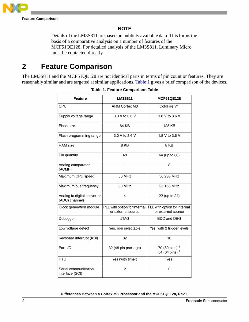
2 Feature ComparisonThe LM3S811 and the MCF51QE128 are not identical parts in terms of pin count or features. They are reasonably similar and are targeted at similar applications. Table 1 gives a brief comparison of the devices.
Table 1. Feature Comparison Table
Feature LM3S811 MCF51QE128
CPU ARM Cortex M3 ColdFire V1
Supply voltage range 3.0 V to 3.6 V 1.8 V to 3.6 V
Flash size 64 KB 128 KB
Flash programming range 3.0 V to 3.6 V 1.8 V to 3.6 V
RAM size 8 KB 8 KB
Pin quantity 48 64 (up to 80)
Analog comparator (ACMP)
1 2
Maximum CPU speed 50 MHz 50.233 MHz
Maximum bus frequency 50 MHz 25.165 MHz
Analog to digital convertor (ADC) channels
4 22 (up to 24)
Clock generation module PLL with option for internal or external source
FLL with option for internal or external source
Debugger JTAG BDC and DBG
Low voltage detect Yes, non selectable Yes, with 2 trigger levels
Keyboard interrupt (KBI) 32 16
Port I/O 32 (48 pin package) 70 (80 pins) 1
54 (64 pins) 1
RTC Yes (with timer) Yes
Serial communication interface (SCI)
2 2
Differences Between a Cortex M3 Processor and the MCF51QE128, Rev. 0
Freescale Semiconductor2
Feature Comparison
1 Port I/O count does not include the input-only PTA5/IRQ/TPM1CLK/RESET or the output-only PTA4/ACMP1O/BKGD/MS.
The following section discusses detailed peripheral differences between the LM3S811 and the MCF51QE128.
All the software examples were developed as described in Section 5, “Software Considerations.”
2.1 Input/Output (I/O)Table 2 shows key parameters of the general-purpose I/O pin circuitry.
The LM3S811 has five GPIO ports. It offers one alternative function for each one of the pins that are selectable by the GPIOAFSEL register. Each port has a data register that is mapped to 256 locations, allowing direct access to individual pins without affecting the state of other pins. The location is selected by using bits 9 through 2.
This functionality translates into two additional operations adding complexity. In some cases it is useful if the address is static. For example, an LED driver that always accesses the same pin.
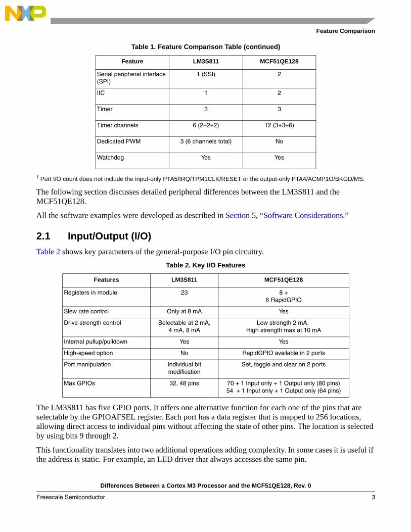
Serial peripheral interface (SPI)
1 (SSI) 2
IIC 1 2
Timer 3 3
Timer channels 6 (2+2+2) 12 (3+3+6)
Dedicated PWM 3 (6 channels total) No
Watchdog Yes Yes
Table 2. Key I/O Features
Features LM3S811 MCF51QE128
Registers in module 23 8 +6 RapidGPIO
Slew rate control Only at 8 mA Yes
Drive strength control Selectable at 2 mA, 4 mA, 8 mA
Low strength 2 mA, High strength max at 10 mA
Internal pullup/pulldown Yes Yes
High-speed option No RapidGPIO available in 2 ports
Port manipulation Individual bit modification
Set, toggle and clear on 2 ports
Max GPIOs 32, 48 pins 70 + 1 Input only + 1 Output only (80 pins)54 + 1 Input only + 1 Output only (64 pins)
Table 1. Feature Comparison Table (continued)
Feature LM3S811 MCF51QE128
Differences Between a Cortex M3 Processor and the MCF51QE128, Rev. 0
Freescale Semiconductor 3
Feature Comparison
The LM3S811 has control of the pin drive strength, slew rate, pulldown/pullup resistor for each pin, and eight read only identification registers used to identify this module as a GPIO.
The MCF51QE128 has nine different ports offering more flexibility with simpler modules. The I/O arrangement allows the user to multiplex up to five different functions for a pin with a simple priority scheme. If a higher priority module is enabled (with a pin enabled), the pin overrides lower priority functions.
Increasing the flexibility of this part, some pins can be routed to other locations to allow more functions in smaller packages.
Ports C and E include the PTxCLR, PTxSET, and PTxTOG registers. This allows easier data manipulation. These registers allow clearing, setting, or toggling individual pins without affecting other pins and without having to perform a read/modify/write value of the port. This offers a similar function to the 256 memory mapped GPIODATA in the LM3S811 with an easier implementation.
The MCF51QE128 has a Rapid GPIO module that allows faster access to the GPIO pins. Port C and E have this alternative function improving performance by connecting the I/O directly to the processor high-speed bus. Rapid GPIO is especially useful when implementing GPIO-intensive functions, as in software based communication protocols.
The GPIO interrupt function is covered in Section 2.2, “Keyboard Interrupt (KBI).”
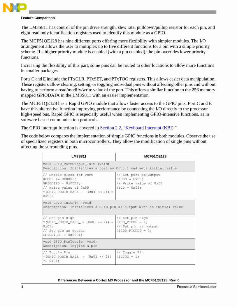
The code below compares the implementation of simple GPIO functions in both modules. Observe the use of specialized registers in both microcontrollers. They allow the modification of single pins without affecting the surrounding pins.
.
LM3S811 MCF51QE128
void GPIO_PortOutput_Init (void)Description: Initializes a port as Output and sets initial value
// Enable clock for Port RCGC2 |= 0x0002; GPIODIRB = 0x00FF;// Write value of 0x55*(GPIO_PORTB_BASE_ + (0xFF << 2)) = 0x55;
// Set port as OutputPTCDD = 0xFF; // Write value of 0x55PTCD = 0x55;
void GPIO_InitPin (void)Description: Initializes a GPIO pin as output with an initial value
// Set pin High*(GPIO_PORTB_BASE_ + (0x01 << 2)) = 0x01;// Set pin as output GPIODIRB |= 0x0001;
// Set pin HighPTCD_PTCD0 = 1;// Set pin as output PTCDD_PTCDD0 = 1;
void GPIO_PinToggle (void)Description: Toggles a pin
// Toggle Pin*(GPIO_PORTB_BASE_ + (0x01 << 2)) ^= 0x01;
// Toggle PinPTCTOG = 1;
Differences Between a Cortex M3 Processor and the MCF51QE128, Rev. 0
Freescale Semiconductor4
Feature Comparison
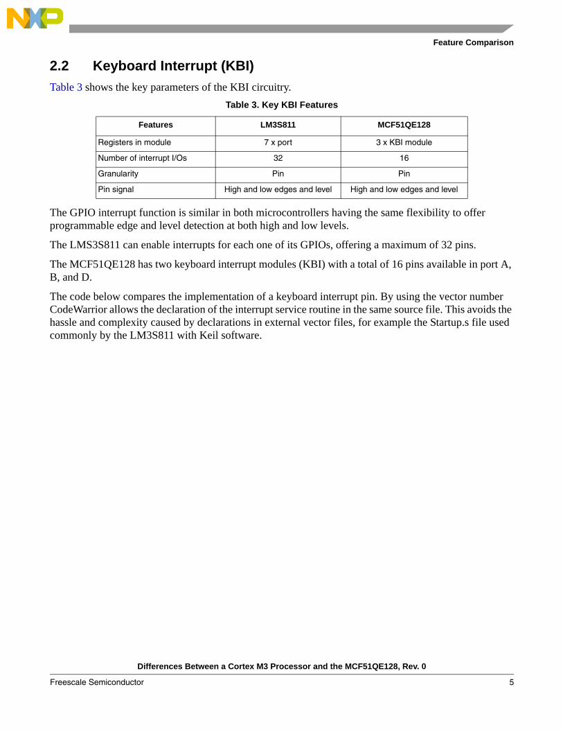
2.2 Keyboard Interrupt (KBI)Table 3 shows the key parameters of the KBI circuitry.
The GPIO interrupt function is similar in both microcontrollers having the same flexibility to offer programmable edge and level detection at both high and low levels.
The LMS3S811 can enable interrupts for each one of its GPIOs, offering a maximum of 32 pins.
The MCF51QE128 has two keyboard interrupt modules (KBI) with a total of 16 pins available in port A, B, and D.
The code below compares the implementation of a keyboard interrupt pin. By using the vector number CodeWarrior allows the declaration of the interrupt service routine in the same source file. This avoids the hassle and complexity caused by declarations in external vector files, for example the Startup.s file used commonly by the LM3S811 with Keil software.
Table 3. Key KBI Features
Features LM3S811 MCF51QE128
Registers in module 7 x port 3 x KBI module
Number of interrupt I/Os 32 16
Granularity Pin Pin
Pin signal High and low edges and level High and low edges and level
Differences Between a Cortex M3 Processor and the MCF51QE128, Rev. 0
Freescale Semiconductor 5
Feature Comparison
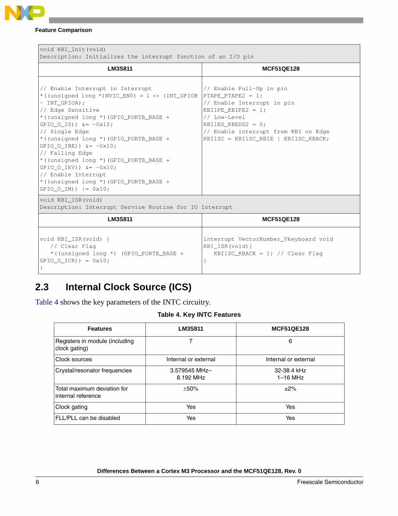
2.3 Internal Clock Source (ICS)Table 4 shows the key parameters of the INTC circuitry.
void KBI_Init(void)Description: Initializes the interrupt function of an I/O pin
LM3S811 MCF51QE128
// Enable Interrupt in Interrupt *((unsigned long *)NVIC_EN0) = 1 << (INT_GPIOB - INT_GPIOA); // Edge Sensitive*((unsigned long *)(GPIO_PORTB_BASE + GPIO_O_IS)) &= ~0x10; // Single Edge*((unsigned long *)(GPIO_PORTB_BASE + GPIO_O_IBE)) &= ~0x10;// Falling Edge*((unsigned long *)(GPIO_PORTB_BASE + GPIO_O_IEV)) &= ~0x10; // Enable Interrupt *((unsigned long *)(GPIO_PORTB_BASE + GPIO_O_IM)) |= 0x10;
// Enable Pull-Up in pin PTAPE_PTAPE2 = 1; // Enable Interrupt in pinKBI1PE_KBIPE2 = 1; // Low-Level KBI1ES_KBEDG2 = 0; // Enable interrupt from KBI on Edge KBI1SC = KBI1SC_KBIE | KBI1SC_KBACK;
void KBI_ISR(void)Description: Interrupt Service Routine for IO Interrupt
LM3S811 MCF51QE128
void KBI_ISR(void) { // Clear Flag *((unsigned long *) (GPIO_PORTB_BASE + GPIO_O_ICR)) = 0x10;}
interrupt VectorNumber_Vkeyboard void KBI_ISR(void){ KBI1SC_KBACK = 1; // Clear Flag}
Table 4. Key INTC Features
Features LM3S811 MCF51QE128
Registers in module (including clock gating)
7 6
Clock sources Internal or external Internal or external
Crystal/resonator frequencies 3.579545 MHz–8.192 MHz
32-38.4 kHz1–16 MHz
Total maximum deviation for internal reference
±50% ±2%
Clock gating Yes Yes
FLL/PLL can be disabled Yes Yes
Differences Between a Cortex M3 Processor and the MCF51QE128, Rev. 0
Freescale Semiconductor6
Feature Comparison
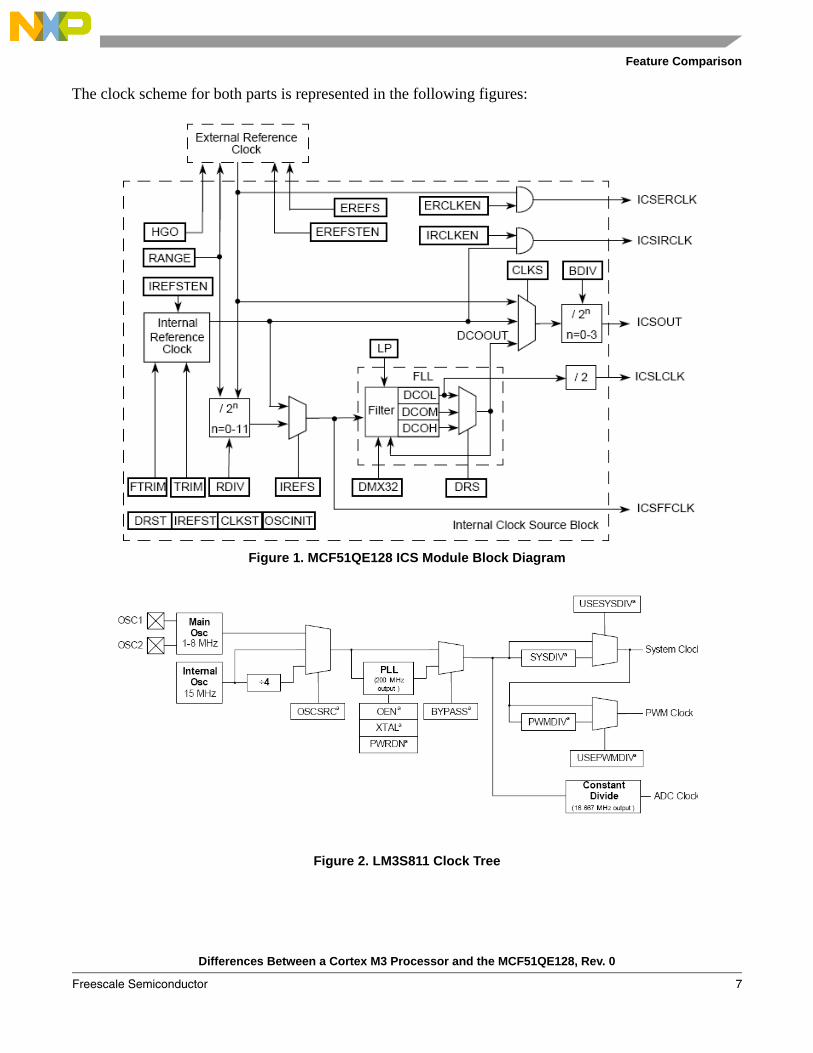
The clock scheme for both parts is represented in the following figures:
Figure 1. MCF51QE128 ICS Module Block Diagram
Figure 2. LM3S811 Clock Tree
Differences Between a Cortex M3 Processor and the MCF51QE128, Rev. 0
Freescale Semiconductor 7
Feature Comparison
Both modules offer similar functions. They can select an internal or external clock source with the option to enable or disable an FLL, (or PLL for the LM3S811) or supply higher frequencies to the processor and bus.
Some differences include an inaccurate internal oscillator on the LM3S811, that is mostly intended to drive the part after reset and/or when accuracy is not required, by offering a ±50% deviation. The MCF51QE128 includes an accurate internal oscillator. After trimmed it can stay within ± 0.2% at a fixed voltage and temperature range, or a ±2% over voltage and temperature.
The MCF51QE128 also includes an option to use low range crystals from 32 kHz – 38.4 kHz. Translating directly into more flexibility with lower cost for the final application and lower-power consumption. This is not offered by the LM3S811.
Both parts offer the function of clock gating. This allows the user to select the parts to be actively driven by the clock. This reduces power consumption. The LM3S811 includes two more registers for clock gating in sleep and deep-sleep modes.
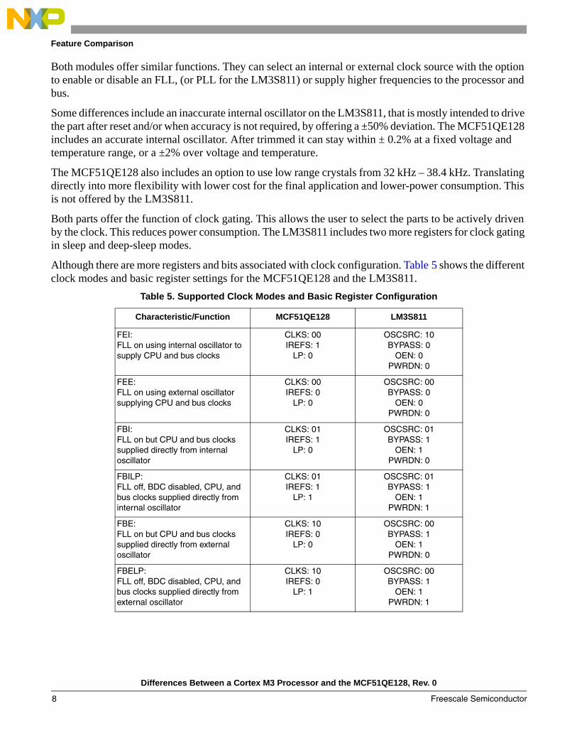
Although there are more registers and bits associated with clock configuration. Table 5 shows the different clock modes and basic register settings for the MCF51QE128 and the LM3S811.
Table 5. Supported Clock Modes and Basic Register Configuration
Characteristic/Function MCF51QE128 LM3S811
FEI: FLL on using internal oscillator to supply CPU and bus clocks
CLKS: 00IREFS: 1
LP: 0
OSCSRC: 10BYPASS: 0
OEN: 0PWRDN: 0
FEE: FLL on using external oscillator supplying CPU and bus clocks
CLKS: 00IREFS: 0
LP: 0
OSCSRC: 00BYPASS: 0
OEN: 0PWRDN: 0
FBI: FLL on but CPU and bus clocks supplied directly from internal oscillator
CLKS: 01IREFS: 1
LP: 0
OSCSRC: 01BYPASS: 1
OEN: 1PWRDN: 0
FBILP: FLL off, BDC disabled, CPU, and bus clocks supplied directly from internal oscillator
CLKS: 01IREFS: 1
LP: 1
OSCSRC: 01BYPASS: 1
OEN: 1PWRDN: 1
FBE:FLL on but CPU and bus clocks supplied directly from external oscillator
CLKS: 10IREFS: 0
LP: 0
OSCSRC: 00BYPASS: 1
OEN: 1PWRDN: 0
FBELP:FLL off, BDC disabled, CPU, and bus clocks supplied directly from external oscillator
CLKS: 10IREFS: 0
LP: 1
OSCSRC: 00BYPASS: 1
OEN: 1PWRDN: 1
Differences Between a Cortex M3 Processor and the MCF51QE128, Rev. 0
Freescale Semiconductor8
Feature Comparison
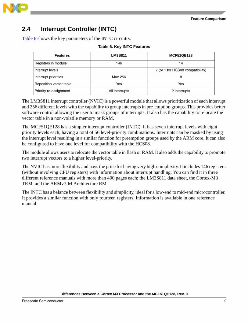
2.4 Interrupt Controller (INTC)Table 6 shows the key parameters of the INTC circuitry.
The LM3S811 interrupt controller (NVIC) is a powerful module that allows prioritization of each interrupt and 256 different levels with the capability to group interrupts in pre-emption groups. This provides better software control allowing the user to mask groups of interrupts. It also has the capability to relocate the vector table in a non-volatile memory or RAM.
The MCF51QE128 has a simpler interrupt controller (INTC). It has seven interrupt levels with eight priority levels each, having a total of 56 level-priority combinations. Interrupts can be masked by using the interrupt level resulting in a similar function for preemption groups used by the ARM core. It can also be configured to have one level for compatibility with the HCS08.
The module allows users to relocate the vector table in flash or RAM. It also adds the capability to promote two interrupt vectors to a higher level-priority.
The NVIC has more flexibility and pays the price for having very high complexity. It includes 146 registers (without involving CPU registers) with information about interrupt handling. You can find it in three different reference manuals with more than 400 pages each; the LM3S811 data sheet, the Cortex-M3 TRM, and the ARMv7-M Architecture RM.
The INTC has a balance between flexibility and simplicity, ideal for a low-end to mid-end microcontroller. It provides a similar function with only fourteen registers. Information is available in one reference manual.
Table 6. Key INTC Features
Features LM3S811 MCF51QE128
Registers in module 146 14
Interrupt levels 7 (or 1 for HCS08 compatibility)
Interrupt priorities Max 256 8
Reposition vector table Yes Yes
Priority re-assignment All interrupts 2 interrupts
Differences Between a Cortex M3 Processor and the MCF51QE128, Rev. 0
Freescale Semiconductor 9
Feature Comparison
2.5 Analog Comparators (ACMP)Table 7 gives a quick overview of the key ACMP parameters, showing the specifics of both parts’ modules.
The analog comparator is a module in both microcontrollers similar in functions. Both have the capability to interrupt the microcontroller, trigger another event, enable an internal reference to the non-inverting input, enable/disable a comparator output, and wake the microcontroller from a low-power mode.
One of the differences between the LM3S811 and the MCF51QE128 is the capability they have for configuring the internal reference. The LM3S811 configures the internal reference at two different ranges with steps defined by 4-bits of the ACREFTL register and 32 options from 0.0 to 2.37 V. The MCF51QE128 can enable an internal bandgap fixed at 1.2 V.
Another feature of both microcontrollers is the flexibility to route the interrupt to a second peripheral. In the LM3S811, the ACMP can signal an event to the ADC channel. This is useful to start a conversion when the comparison is met. The MCF51QE128 can be configured to send the output of the analog comparator to the timer input capture channel offering flexibility for motor control functions.
The code below compares the implementation of a simple ACMP configuration. The table uses interrupts to detect a rising or falling edge and using both the inverting and non-inverting inputs.
Table 7. Key Analog Comparator Features
Features LMS3S811 MCF51QE128
Registers in module 6 1
Internal reference 16 steps from0.825 V - 2.37 V or0.0 V – 2.0625 V
1.2 V
Input options Two pins or internal reference on non-inverting input
Two pins or internal reference on non-inverting input
Additional trigger options Can trigger the ADC Can trigger a timer input capture channel
Differences Between a Cortex M3 Processor and the MCF51QE128, Rev. 0
Freescale Semiconductor10
Feature Comparison
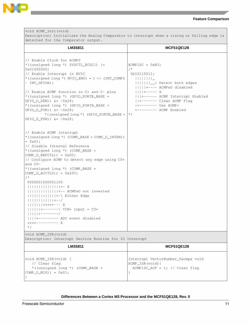
void ACMP_Init(void)Description: Initializes the Analog Comparator to interrupt when a rising or falling edge is detected for the Comparator output.
LM3S811 MCF51QE128
// Enable Clock for ACMP0*((unsigned long *) SYSCTL_RCGC1) |= 0x01000000;// Enable Interrupt in NVIC*((unsigned long *) NVIC_EN0) = 1 << (INT_COMP0 - INT_GPIOA);
// Enable ACMP function in C+ and C- pins*((unsigned long *) (GPIO_PORTB_BASE + GPIO_O_DEN)) &= ~0x28;*((unsigned long *) (GPIO_PORTB_BASE + GPIO_O_PUR)) &= ~0x28;
*((unsigned long *) (GPIO_PORTB_BASE + GPIO_O_PDR)) &= ~0x28;
// Enable ACMP interrupt*((unsigned long *) (COMP_BASE + COMP_O_INTEN)) = 0x01;// Disable Internal Reference*((unsigned long *) (COMP_BASE + COMP_O_REFCTL)) = 0x00;// Configure ACMP to detect any edge using C0+ and C0- *((unsigned long *) (COMP_BASE + COMP_O_ACCTL0)) = 0x20C;/* 0000001000001100 |||||||||||||||+- X ||||||||||||||+-- ACMPxO not inverted |||||||||||||+-\ Either Edge ||||||||||||+--/ |||||||+++++--- X ||||||+-------\ VIN+ input = C0+ |||||+--------/ ||||+--------- ADC event disabled ++++---------- X */
ACMP1SC = 0xB3; /* 0b10110011; ||||||||_ |||||||__> Detect both edges |||||+---- ACMPxO disabled ||||+----- X |||+------ ACMP Interrupt Enabled ||+------- Clear ACMP Flag |+-------- Use ACMP+ +--------- ACMP Enabled*/
void ACMP_ISR(void)Description: Interrupt Service Routine for IO Interrupt
LM3S811 MCF51QE128
void ACMP_ISR(void) { // Clear flag *((unsigned long *) (COMP_BASE + COMP_O_MIS)) = 0x01;}
interrupt VectorNumber_Vacmpx void ACMP_ISR(void){ ACMP1SC_ACF = 1; // Clear flag}
Differences Between a Cortex M3 Processor and the MCF51QE128, Rev. 0
Freescale Semiconductor 11
Feature Comparison
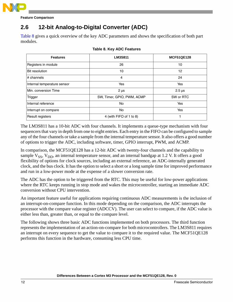
2.6 12-bit Analog-to-Digital Converter (ADC)Table 8 gives a quick overview of the key ADC parameters and shows the specification of both part modules.
The LM3S811 has a 10-bit ADC with four channels. It implements a queue-type mechanism with four sequencers that vary in depth from one to eight entries. Each entry in the FIFO can be configured to sample any of the four channels or take a sample from the internal temperature sensor. It also offers a good number of options to trigger the ADC, including software, timer, GPIO interrupt, PWM, and ACMP.
In comparison, the MCF51QE128 has a 12-bit ADC with twenty-four channels and the capability to sample VSS, VDD, an internal temperature sensor, and an internal bandgap at 1.2 V. It offers a good flexibility of options for clock sources, including an external reference, an ADC-internally generated clock, and the bus clock. It has the option to select a short or a long sample time for improved performance and run in a low-power mode at the expense of a slower conversion rate.
The ADC has the option to be triggered from the RTC. This may be useful for low-power applications where the RTC keeps running in stop mode and wakes the microcontroller, starting an immediate ADC conversion without CPU intervention.
An important feature useful for applications requiring continuous ADC measurements is the inclusion of an interrupt-on-compare function. In this mode depending on the comparison, the ADC interrupts the processor with the compare value register (ADCCV). The user can select to compare, if the ADC value is either less than, greater than, or equal to the compare level.
The following shows three basic ADC functions implemented on both processors. The third function represents the implementation of an action-on-compare for both microcontrollers. The LM3S811 requires an interrupt on every sequence to get the value to compare it to the required value. The MCF51QE128 performs this function in the hardware, consuming less CPU time.
Table 8. Key ADC Features
Features LM3S811 MCF51QE128
Registers in module 26 10
Bit resolution 10 12
# channels 4 24
Internal temperature sensor Yes Yes
Min. conversion Time 2 µs 2.5 µs
Trigger SW, Timer, GPIO, PWM, ACMP SW or RTC
Internal reference No Yes
Interrupt on compare No Yes
Result registers 4 (with FIFO of 1 to 8) 1
Differences Between a Cortex M3 Processor and the MCF51QE128, Rev. 0
Freescale Semiconductor12
Feature Comparison
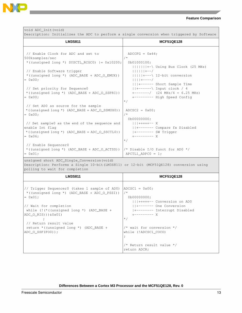
void ADC_Init(void)Description: Initializes the ADC to perform a single conversion when triggered by Software
LM3S811 MCF51QE128
// Enable Clock for ADC and set to 500ksamples/sec *((unsigned long *) SYSCTL_RCGC0) |= 0x10200;
// Enable Software trigger *((unsigned long *) (ADC_BASE + ADC_O_EMUX)) = 0x00;
// Set priority for Sequence0 *((unsigned long *) (ADC_BASE + ADC_O_SSPRI)) = 0x00;
// Set AD0 as source for the sample *((unsigned long *) (ADC_BASE + ADC_O_SSMUX0)) = 0x00;
// Set sample0 as the end of the sequence and enable Int flag *((unsigned long *) (ADC_BASE + ADC_O_SSCTL0)) = 0x06;
// Enable Sequencer0 *((unsigned long *) (ADC_BASE + ADC_O_ACTSS)) = 0x01;
ADCCFG = 0x44;/* 0b01000100; |||||||+-\ Using Bus Clock (25 MHz) ||||||+--/ |||||+---\ 12-bit conversion ||||+----/ |||+------ Short Sample Time ||+------\ Input clock / 4 +-------/ (24 MHz/4 = 6.25 MHz) +--------- High Speed Config */
ADCSC2 = 0x00; /* 0b00000000; |||+++++-- X ||+------- Compare fx Disabled |+-------- SW Trigger +--------- X*/
/* Disable I/O funct for AD0 */ APCTL1_ADPC0 = 1;
unsigned short ADC_Single_Conversion(void) Description: Performs a Single 10-bit(LM3S811) or 12-bit (MCF51QE128) conversion using polling to wait for completion
LM3S811 MCF51QE128
// Trigger Sequencer0 (takes 1 sample of AD0) *((unsigned long *) (ADC_BASE + ADC_O_PSSI)) = 0x01;
// Wait for completion while (!(*((unsigned long *) (ADC_BASE + ADC_O_RIS)))&0x01)
; // Return result value return *((unsigned long *) (ADC_BASE + ADC_O_SSFIFO0));
ADCSC1 = 0x00; /* 0b00000000; |||+++++-- Conversion on AD0 ||+------- One Conversion |+-------- Interrupt Disabled +--------- X*/
/* wait for conversion */while (!ADCSC1_COCO) ;
/* Return result value */return ADCR;
Differences Between a Cortex M3 Processor and the MCF51QE128, Rev. 0
Freescale Semiconductor 13
Feature Comparison
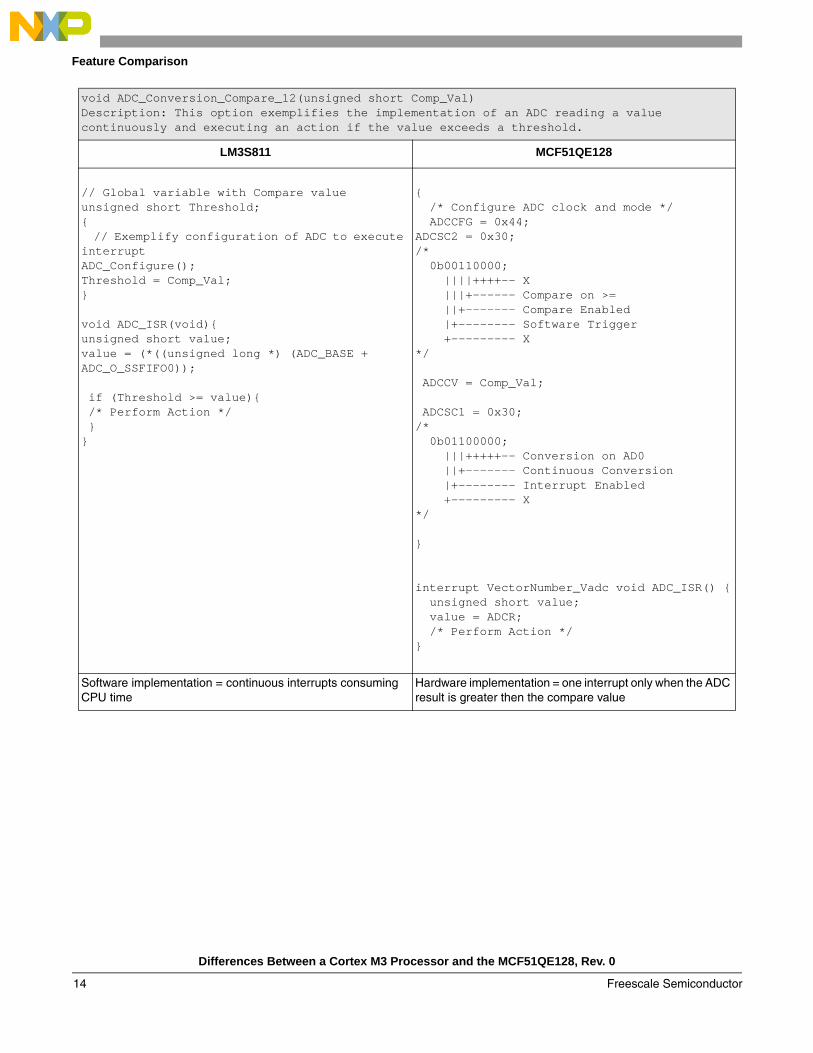
void ADC_Conversion_Compare_12(unsigned short Comp_Val)Description: This option exemplifies the implementation of an ADC reading a value continuously and executing an action if the value exceeds a threshold.
LM3S811 MCF51QE128
// Global variable with Compare valueunsigned short Threshold;{ // Exemplify configuration of ADC to execute interruptADC_Configure();Threshold = Comp_Val;}
void ADC_ISR(void){unsigned short value;value = (*((unsigned long *) (ADC_BASE + ADC_O_SSFIFO0));
if (Threshold >= value){ /* Perform Action */ }}
{ /* Configure ADC clock and mode */ ADCCFG = 0x44;ADCSC2 = 0x30;/* 0b00110000; ||||++++-- X |||+------ Compare on >= ||+------- Compare Enabled |+-------- Software Trigger +--------- X*/ ADCCV = Comp_Val; ADCSC1 = 0x30;/* 0b01100000; |||+++++-- Conversion on AD0 ||+------- Continuous Conversion |+-------- Interrupt Enabled +--------- X*/
}
interrupt VectorNumber_Vadc void ADC_ISR() { unsigned short value; value = ADCR; /* Perform Action */}
Software implementation = continuous interrupts consuming CPU time
Hardware implementation = one interrupt only when the ADC result is greater then the compare value
Differences Between a Cortex M3 Processor and the MCF51QE128, Rev. 0
Freescale Semiconductor14
Feature Comparison
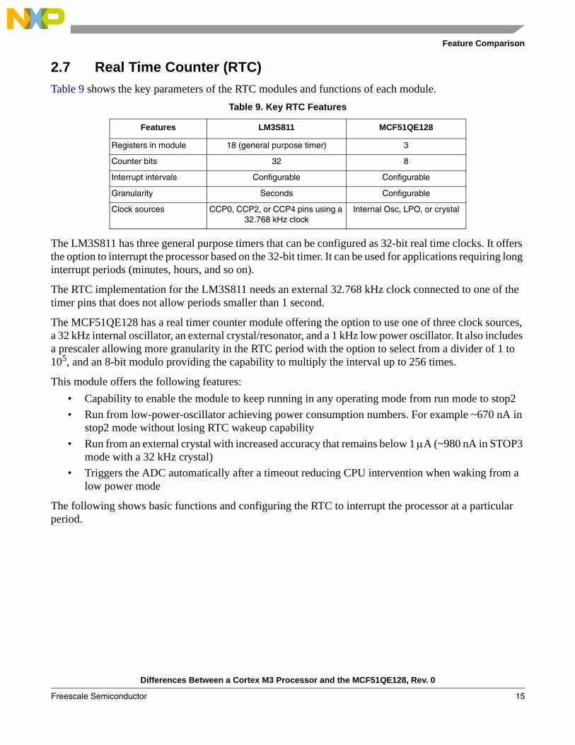
2.7 Real Time Counter (RTC)Table 9 shows the key parameters of the RTC modules and functions of each module.
The LM3S811 has three general purpose timers that can be configured as 32-bit real time clocks. It offers the option to interrupt the processor based on the 32-bit timer. It can be used for applications requiring long interrupt periods (minutes, hours, and so on).
The RTC implementation for the LM3S811 needs an external 32.768 kHz clock connected to one of the timer pins that does not allow periods smaller than 1 second.
The MCF51QE128 has a real timer counter module offering the option to use one of three clock sources, a 32 kHz internal oscillator, an external crystal/resonator, and a 1 kHz low power oscillator. It also includes a prescaler allowing more granularity in the RTC period with the option to select from a divider of 1 to 105, and an 8-bit modulo providing the capability to multiply the interval up to 256 times.
This module offers the following features:• Capability to enable the module to keep running in any operating mode from run mode to stop2• Run from low-power-oscillator achieving power consumption numbers. For example ~670 nA in
stop2 mode without losing RTC wakeup capability• Run from an external crystal with increased accuracy that remains below 1 μA (~980 nA in STOP3
mode with a 32 kHz crystal)• Triggers the ADC automatically after a timeout reducing CPU intervention when waking from a
low power mode
The following shows basic functions and configuring the RTC to interrupt the processor at a particular period.
Table 9. Key RTC Features
Features LM3S811 MCF51QE128
Registers in module 18 (general purpose timer) 3
Counter bits 32 8
Interrupt intervals Configurable Configurable
Granularity Seconds Configurable
Clock sources CCP0, CCP2, or CCP4 pins using a 32.768 kHz clock
Internal Osc, LPO, or crystal
Differences Between a Cortex M3 Processor and the MCF51QE128, Rev. 0
Freescale Semiconductor 15
Feature Comparison
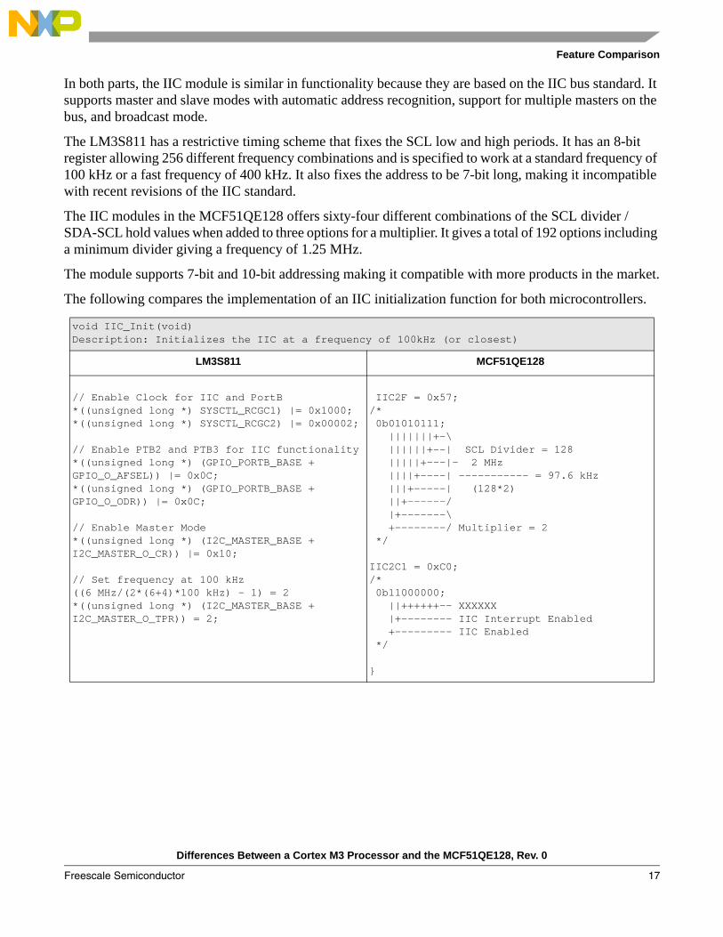
2.8 Inter-Integrated Circuit (IIC)Table 11 shows the key parameters of the IIC module in both microcontrollers.
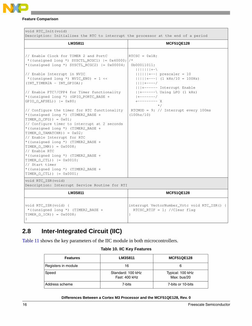
void RTC_Init(void)Description: Initializes the RTC to interrupt the processor at the end of a period
LM3S811 MCF51QE128
// Enable Clock for TIMER 2 and PortC *((unsigned long *) SYSCTL_RCGC1) |= 0x40000;*((unsigned long *) SYSCTL_RCGC2) |= 0x00004; // Enable Interrupt in NVIC *((unsigned long *) NVIC_EN0) = 1 << (INT_TIMER2A - INT_GPIOA);
// Enable PTC7/CPP4 for Timer functionality*((unsigned long *) (GPIO_PORTC_BASE + GPIO_O_AFSEL)) |= 0x80;
// Configure the timer for RTC functionality*((unsigned long *) (TIMER2_BASE + TIMER_O_CFG)) = 0x01;// Configure timer to interrupt at 2 seconds*((unsigned long *) (TIMER2_BASE + TIMER_O_TAMATCHR)) = 0x02;// Enable Interrupt for RTC*((unsigned long *) (TIMER2_BASE + TIMER_O_IMR)) = 0x0008;// Enable RTC*((unsigned long *) (TIMER2_BASE + TIMER_O_CTL)) |= 0x0010;// Start timer*((unsigned long *) (TIMER2_BASE + TIMER_O_CTL)) |= 0x0001;
RTCSC = 0x1B;/* 0b00011011; |||||||+-\ ||||||+--| prescaler = 10 |||||+---| (1 kHz/10 = 100Hz) ||||+----/ |||+------ Interrupt Enable ||+------\ Using LPO (1 kHz) |+-------/ +--------- X */ RTCMOD = 9; // Interrupt every 100ms(100hz/10)
void RTC_ISR(void)Description: Interrupt Service Routine for RTI
LM3S811 MCF51QE128
void RTC_ISR(void) { *((unsigned long *) (TIMER2_BASE + TIMER_O_ICR)) = 0x0008; }
interrupt VectorNumber_Vrtc void RTC_ISR() { RTCSC_RTIF = 1; //Clear flag}
Table 10. IIC Key Features
Features LM3S811 MCF51QE128
Registers in module 16 6
Speed Standard: 100 kHz Fast: 400 kHz
Typical: 100 kHz Max: bus/20
Address scheme 7-bits 7-bits or 10-bits
Differences Between a Cortex M3 Processor and the MCF51QE128, Rev. 0
Freescale Semiconductor16
Feature Comparison
In both parts, the IIC module is similar in functionality because they are based on the IIC bus standard. It supports master and slave modes with automatic address recognition, support for multiple masters on the bus, and broadcast mode.
The LM3S811 has a restrictive timing scheme that fixes the SCL low and high periods. It has an 8-bit register allowing 256 different frequency combinations and is specified to work at a standard frequency of 100 kHz or a fast frequency of 400 kHz. It also fixes the address to be 7-bit long, making it incompatible with recent revisions of the IIC standard.
The IIC modules in the MCF51QE128 offers sixty-four different combinations of the SCL divider / SDA-SCL hold values when added to three options for a multiplier. It gives a total of 192 options including a minimum divider giving a frequency of 1.25 MHz.
The module supports 7-bit and 10-bit addressing making it compatible with more products in the market.
The following compares the implementation of an IIC initialization function for both microcontrollers.
void IIC_Init(void)Description: Initializes the IIC at a frequency of 100kHz (or closest)
LM3S811 MCF51QE128
// Enable Clock for IIC and PortB*((unsigned long *) SYSCTL_RCGC1) |= 0x1000;*((unsigned long *) SYSCTL_RCGC2) |= 0x00002;
// Enable PTB2 and PTB3 for IIC functionality*((unsigned long *) (GPIO_PORTB_BASE + GPIO_O_AFSEL)) |= 0x0C;*((unsigned long *) (GPIO_PORTB_BASE + GPIO_O_ODR)) |= 0x0C;
// Enable Master Mode*((unsigned long *) (I2C_MASTER_BASE + I2C_MASTER_O_CR)) |= 0x10;
// Set frequency at 100 kHz ((6 MHz/(2*(6+4)*100 kHz) - 1) = 2*((unsigned long *) (I2C_MASTER_BASE + I2C_MASTER_O_TPR)) = 2;
IIC2F = 0x57;/* 0b01010111; |||||||+-\ ||||||+--| SCL Divider = 128 |||||+---|- 2 MHz ||||+----| ----------- = 97.6 kHz |||+-----| (128*2) ||+------/ |+-------\ +--------/ Multiplier = 2 */
IIC2C1 = 0xC0;/* 0b11000000; ||++++++-- XXXXXX |+-------- IIC Interrupt Enabled +--------- IIC Enabled */ }
Differences Between a Cortex M3 Processor and the MCF51QE128, Rev. 0
Freescale Semiconductor 17
Feature Comparison
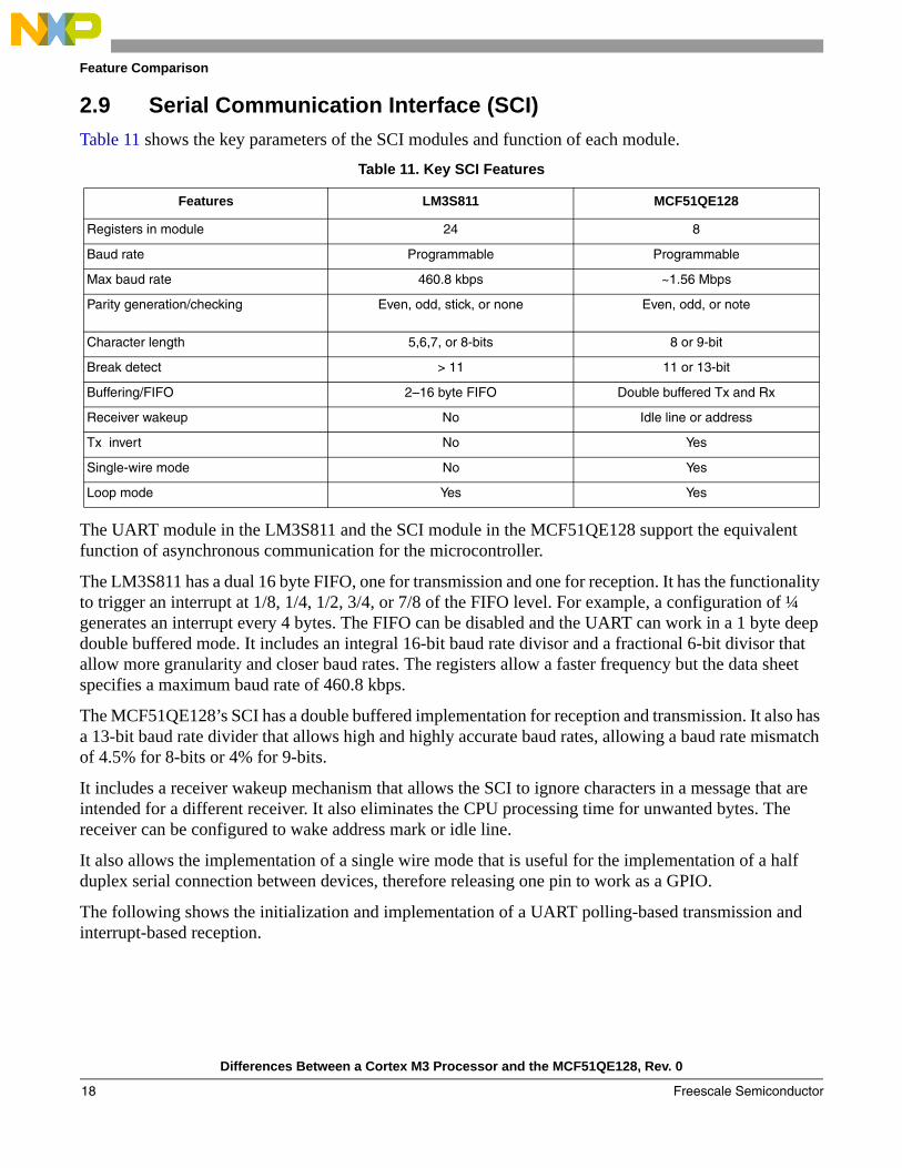
2.9 Serial Communication Interface (SCI)Table 11 shows the key parameters of the SCI modules and function of each module.
The UART module in the LM3S811 and the SCI module in the MCF51QE128 support the equivalent function of asynchronous communication for the microcontroller.
The LM3S811 has a dual 16 byte FIFO, one for transmission and one for reception. It has the functionality to trigger an interrupt at 1/8, 1/4, 1/2, 3/4, or 7/8 of the FIFO level. For example, a configuration of ¼ generates an interrupt every 4 bytes. The FIFO can be disabled and the UART can work in a 1 byte deep double buffered mode. It includes an integral 16-bit baud rate divisor and a fractional 6-bit divisor that allow more granularity and closer baud rates. The registers allow a faster frequency but the data sheet specifies a maximum baud rate of 460.8 kbps.
The MCF51QE128’s SCI has a double buffered implementation for reception and transmission. It also has a 13-bit baud rate divider that allows high and highly accurate baud rates, allowing a baud rate mismatch of 4.5% for 8-bits or 4% for 9-bits.
It includes a receiver wakeup mechanism that allows the SCI to ignore characters in a message that are intended for a different receiver. It also eliminates the CPU processing time for unwanted bytes. The receiver can be configured to wake address mark or idle line.
It also allows the implementation of a single wire mode that is useful for the implementation of a half duplex serial connection between devices, therefore releasing one pin to work as a GPIO.
The following shows the initialization and implementation of a UART polling-based transmission and interrupt-based reception.
Table 11. Key SCI Features
Features LM3S811 MCF51QE128
Registers in module 24 8
Baud rate Programmable Programmable
Max baud rate 460.8 kbps ~1.56 Mbps
Parity generation/checking Even, odd, stick, or none Even, odd, or note
Character length 5,6,7, or 8-bits 8 or 9-bit
Break detect > 11 11 or 13-bit
Buffering/FIFO 2–16 byte FIFO Double buffered Tx and Rx
Receiver wakeup No Idle line or address
Tx invert No Yes
Single-wire mode No Yes
Loop mode Yes Yes
Differences Between a Cortex M3 Processor and the MCF51QE128, Rev. 0
Freescale Semiconductor18
Feature Comparison
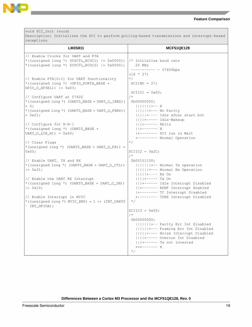
void SCI_Init (void)Description: Initializes the SCI to perform polling-based transmissions and interrupt-based receptions
LM3S811 MCF51QE128
// Enable Clocks for UART and PTA*((unsigned long *) SYSCTL_RCGC1) |= 0x00001;*((unsigned long *) SYSCTL_RCGC2) |= 0x00001;
// Enable PTA[0:1] for UART functionality*((unsigned long *) (GPIO_PORTA_BASE + GPIO_O_AFSEL)) |= 0x03; // Configure UART at 57600*((unsigned long *) (UART0_BASE + UART_O_IBRD)) = 6;*((unsigned long *) (UART0_BASE + UART_O_FBRD)) = 0x21;
// Configure for 8-N-1*((unsigned long *) (UART0_BASE + UART_O_LCR_H)) = 0x60;
// Clear Flags*(unsigned long *) (UART0_BASE + UART_O_FR)) = 0x00;
// Enable UART, TX and RX*((unsigned long *) (UART0_BASE + UART_O_CTL)) |= 0x31;
// Enable the UART RX Interrupt*((unsigned long *) (UART0_BASE + UART_O_IM)) |= 0x10;
// Enable Interrupt in NVIC*((unsigned long *) NVIC_EN0) = 1 << (INT_UART0 - INT_GPIOA);
/* Initialize baud rate 25 MHz ----------- ~ 57600bps(16 * 27) */ SCI1BD = 27;
SCI1C1 = 0x00;/* 0b00000000; |||||||+-- X ||||||+--- No Parity |||||+---- Idle after start bit ||||+----- Idle-Wakeup |||+------ 8bits ||+------- X |+-------- SCI run in Wait +--------- Normal Operation*/
SCI1C2 = 0x2C;/* 0b00101100; |||||||+-- Normal Tx operation ||||||+--- Normal Rx Operation |||||+---- Rx On ||||+----- Tx On |||+------ Idle Interrupt Disabled ||+------- RDRF Interrupt Enabled |+-------- TC Interrupt Disabled +--------- TDRE Interrupt Disabled */
SCI1C3 = 0x00;/* 0b00000000; |||||||+-- Parity Err Int Disabled ||||||+--- Framing Err Int Disabled |||||+---- Noise Interrupt Disabled ||||+----- Overrun Int Disabled |||+------ Tx not inverted +++------- X */
Differences Between a Cortex M3 Processor and the MCF51QE128, Rev. 0
Freescale Semiconductor 19
Feature Comparison
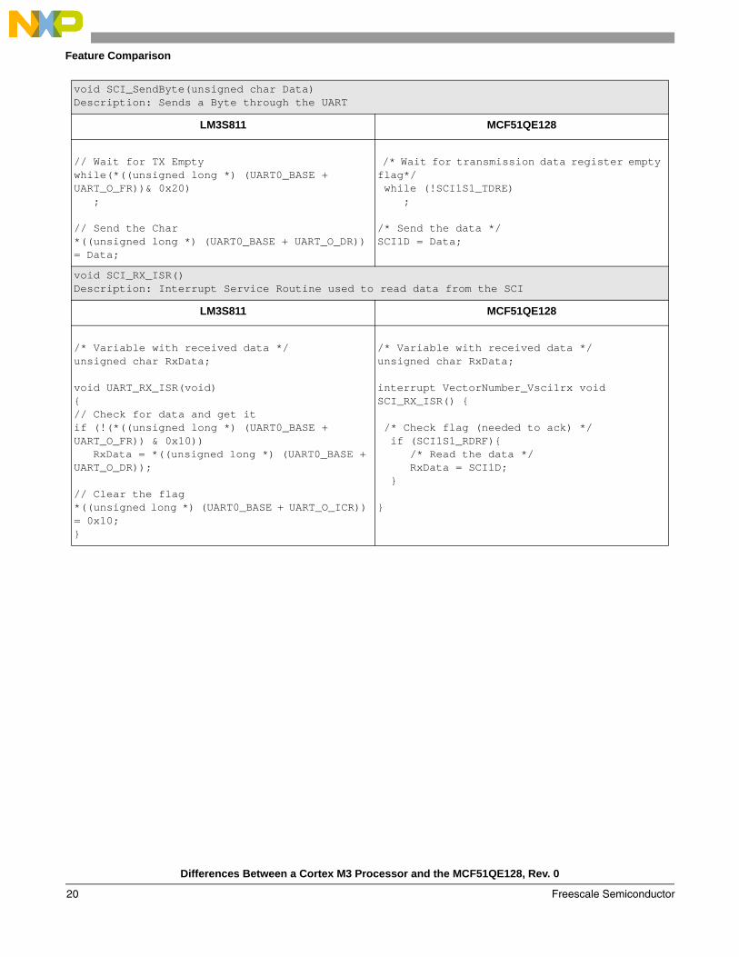
void SCI_SendByte(unsigned char Data)Description: Sends a Byte through the UART
LM3S811 MCF51QE128
// Wait for TX Emptywhile(*((unsigned long *) (UART0_BASE + UART_O_FR))& 0x20) ;
// Send the Char *((unsigned long *) (UART0_BASE + UART_O_DR)) = Data;
/* Wait for transmission data register empty flag*/ while (!SCI1S1_TDRE) ; /* Send the data */SCI1D = Data;
void SCI_RX_ISR()Description: Interrupt Service Routine used to read data from the SCI
LM3S811 MCF51QE128
/* Variable with received data */unsigned char RxData;
void UART_RX_ISR(void){// Check for data and get itif (!(*((unsigned long *) (UART0_BASE + UART_O_FR)) & 0x10)) RxData = *((unsigned long *) (UART0_BASE + UART_O_DR)); // Clear the flag*((unsigned long *) (UART0_BASE + UART_O_ICR)) = 0x10;}
/* Variable with received data */unsigned char RxData;
interrupt VectorNumber_Vsci1rx void SCI_RX_ISR() { /* Check flag (needed to ack) */ if (SCI1S1_RDRF){ /* Read the data */ RxData = SCI1D; }
}
Differences Between a Cortex M3 Processor and the MCF51QE128, Rev. 0
Freescale Semiconductor20
Feature Comparison
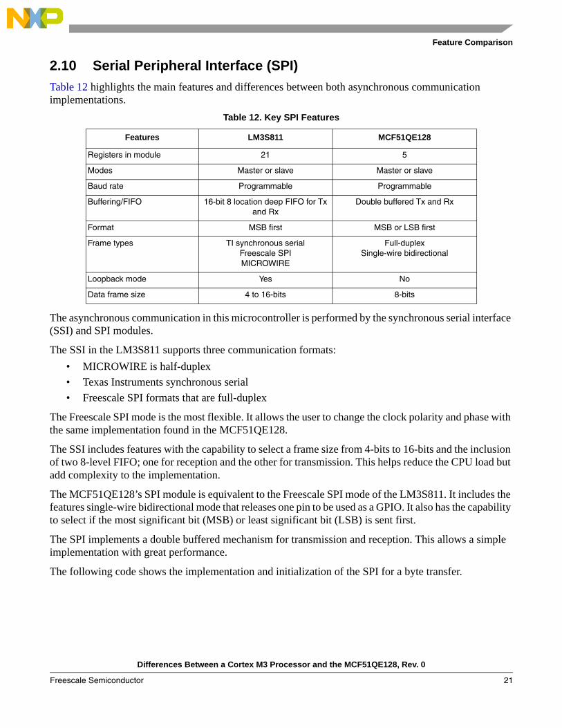
2.10 Serial Peripheral Interface (SPI)Table 12 highlights the main features and differences between both asynchronous communication implementations.
The asynchronous communication in this microcontroller is performed by the synchronous serial interface (SSI) and SPI modules.
The SSI in the LM3S811 supports three communication formats:• MICROWIRE is half-duplex• Texas Instruments synchronous serial• Freescale SPI formats that are full-duplex
The Freescale SPI mode is the most flexible. It allows the user to change the clock polarity and phase with the same implementation found in the MCF51QE128.
The SSI includes features with the capability to select a frame size from 4-bits to 16-bits and the inclusion of two 8-level FIFO; one for reception and the other for transmission. This helps reduce the CPU load but add complexity to the implementation.
The MCF51QE128’s SPI module is equivalent to the Freescale SPI mode of the LM3S811. It includes the features single-wire bidirectional mode that releases one pin to be used as a GPIO. It also has the capability to select if the most significant bit (MSB) or least significant bit (LSB) is sent first.
The SPI implements a double buffered mechanism for transmission and reception. This allows a simple implementation with great performance.
The following code shows the implementation and initialization of the SPI for a byte transfer.
Table 12. Key SPI Features
Features LM3S811 MCF51QE128
Registers in module 21 5
Modes Master or slave Master or slave
Baud rate Programmable Programmable
Buffering/FIFO 16-bit 8 location deep FIFO for Tx and Rx
Double buffered Tx and Rx
Format MSB first MSB or LSB first
Frame types TI synchronous serialFreescale SPIMICROWIRE
Full-duplexSingle-wire bidirectional
Loopback mode Yes No
Data frame size 4 to 16-bits 8-bits
Differences Between a Cortex M3 Processor and the MCF51QE128, Rev. 0
Freescale Semiconductor 21
Feature Comparison
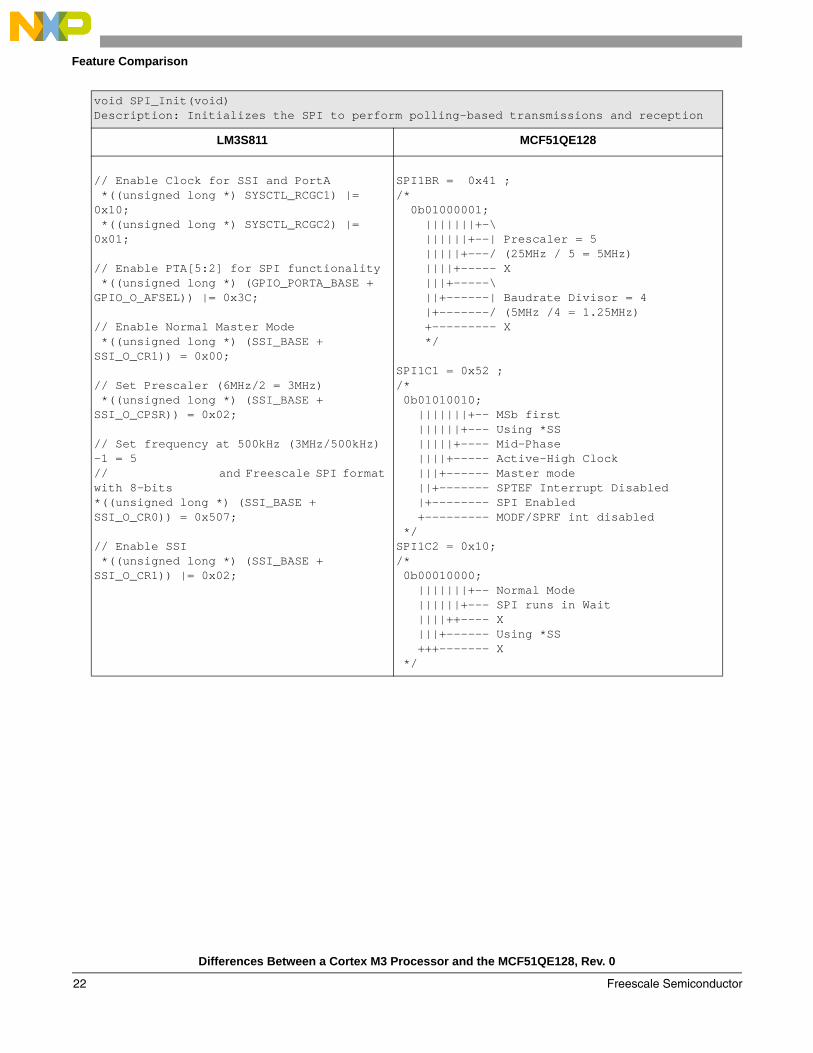
void SPI_Init(void)Description: Initializes the SPI to perform polling-based transmissions and reception
LM3S811 MCF51QE128
// Enable Clock for SSI and PortA *((unsigned long *) SYSCTL_RCGC1) |= 0x10; *((unsigned long *) SYSCTL_RCGC2) |= 0x01;
// Enable PTA[5:2] for SPI functionality *((unsigned long *) (GPIO_PORTA_BASE + GPIO_O_AFSEL)) |= 0x3C; // Enable Normal Master Mode *((unsigned long *) (SSI_BASE + SSI_O_CR1)) = 0x00;
// Set Prescaler (6MHz/2 = 3MHz) *((unsigned long *) (SSI_BASE + SSI_O_CPSR)) = 0x02;
// Set frequency at 500kHz (3MHz/500kHz) -1 = 5 // and Freescale SPI format with 8-bits*((unsigned long *) (SSI_BASE + SSI_O_CR0)) = 0x507;
// Enable SSI *((unsigned long *) (SSI_BASE + SSI_O_CR1)) |= 0x02;
SPI1BR = 0x41 ;/* 0b01000001; |||||||+-\ ||||||+--| Prescaler = 5 |||||+---/ (25MHz / 5 = 5MHz) ||||+----- X |||+-----\ ||+------| Baudrate Divisor = 4 |+-------/ (5MHz /4 = 1.25MHz) +--------- X */
SPI1C1 = 0x52 ;/* 0b01010010; |||||||+-- MSb first ||||||+--- Using *SS |||||+---- Mid-Phase ||||+----- Active-High Clock |||+------ Master mode ||+------- SPTEF Interrupt Disabled |+-------- SPI Enabled +--------- MODF/SPRF int disabled */SPI1C2 = 0x10;/* 0b00010000; |||||||+-- Normal Mode ||||||+--- SPI runs in Wait ||||++---- X |||+------ Using *SS +++------- X */
Differences Between a Cortex M3 Processor and the MCF51QE128, Rev. 0
Freescale Semiconductor22
Feature Comparison
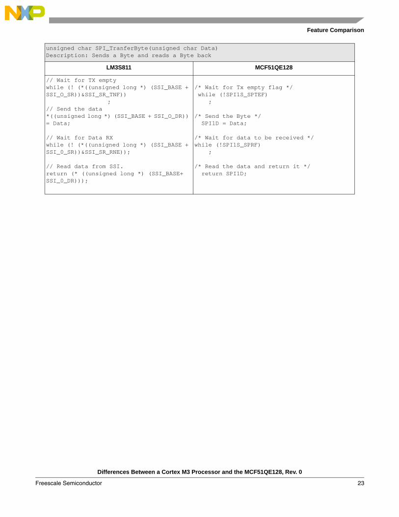
unsigned char SPI_TranferByte(unsigned char Data)Description: Sends a Byte and reads a Byte back
LM3S811 MCF51QE128
// Wait for TX emptywhile (! (*((unsigned long *) (SSI_BASE + SSI_O_SR))&SSI_SR_TNF))
;// Send the data*((unsigned long *) (SSI_BASE + SSI_O_DR)) = Data;
// Wait for Data RXwhile (! (*((unsigned long *) (SSI_BASE + SSI_0_SR))&SSI_SR_RNE));
// Read data from SSI.return (* ((unsigned long *) (SSI_BASE+ SSI_0_DR)));
/* Wait for Tx empty flag */ while (!SPI1S_SPTEF) ;
/* Send the Byte */ SPI1D = Data;
/* Wait for data to be received */while (!SPI1S_SPRF) ;
/* Read the data and return it */ return SPI1D;
Differences Between a Cortex M3 Processor and the MCF51QE128, Rev. 0
Freescale Semiconductor 23
Feature Comparison
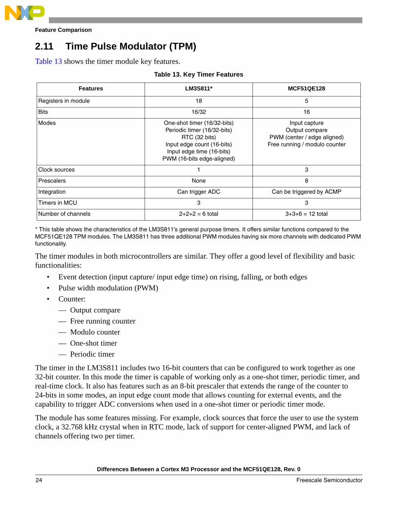
2.11 Time Pulse Modulator (TPM)Table 13 shows the timer module key features.
* This table shows the characteristics of the LM3S811’s general purpose timers. It offers similar functions compared to the MCF51QE128 TPM modules. The LM3S811 has three additional PWM modules having six more channels with dedicated PWM functionality.
The timer modules in both microcontrollers are similar. They offer a good level of flexibility and basic functionalities:
• Event detection (input capture/ input edge time) on rising, falling, or both edges• Pulse width modulation (PWM)• Counter:
— Output compare— Free running counter— Modulo counter— One-shot timer— Periodic timer
The timer in the LM3S811 includes two 16-bit counters that can be configured to work together as one 32-bit counter. In this mode the timer is capable of working only as a one-shot timer, periodic timer, and real-time clock. It also has features such as an 8-bit prescaler that extends the range of the counter to 24-bits in some modes, an input edge count mode that allows counting for external events, and the capability to trigger ADC conversions when used in a one-shot timer or periodic timer mode.
The module has some features missing. For example, clock sources that force the user to use the system clock, a 32.768 kHz crystal when in RTC mode, lack of support for center-aligned PWM, and lack of channels offering two per timer.
Table 13. Key Timer Features
Features LM3S811* MCF51QE128
Registers in module 18 5
Bits 16/32 16
Modes One-shot timer (16/32-bits)Periodic timer (16/32-bits)
RTC (32 bits)Input edge count (16-bits)Input edge time (16-bits)
PWM (16-bits edge-aligned)
Input captureOutput compare
PWM (center / edge aligned)Free running / modulo counter
Clock sources 1 3
Prescalers None 8
Integration Can trigger ADC Can be triggered by ACMP
Timers in MCU 3 3
Number of channels 2+2+2 = 6 total 3+3+6 = 12 total
Differences Between a Cortex M3 Processor and the MCF51QE128, Rev. 0
Freescale Semiconductor24
Feature Comparison
The LM3S811 also includes a 16-bit PWM module capable of performing edge or center-aligned PWMs with the flexibility to generate complimentary signals with dead-time insertion.
The MCF51QE128 has one main 16-bit counter for each of its three timers and the functionalities shared in common with the LM3S81. It has the capability to run center-aligned PWMs within the same module and flexibility for clock sources. It can also run from an external source driven by one of the pins that can be as high as ¼ of the bus clock.
The MCF51QE128 implements two TPM modules with 3 channels each and an additional one with 6 channels with a total amount of 12 channels. These can be used for input capture, output compare, or PWM. This gives more flexibility for development.
As mentioned inSection 2.5, “Analog Comparators (ACMP),” the analog comparator output can be connected to the timer channel 0 that can be used to trigger an input capture conversion when a specific voltage level is met.
The following code shows the implementation and initialization of the TPM for an input capture function.
Differences Between a Cortex M3 Processor and the MCF51QE128, Rev. 0
Freescale Semiconductor 25
Feature Comparison
void Timer_Init(void)Description: Initializes the Timer to detect a rising edge
LM3S811 MCF51QE128
// Using PD4/CCP0 *((unsigned long *) SYSCTL_RCGC1) |= 0x00010000; *((unsigned long *) SYSCTL_RCGC2) |= 0x00000008;
// Enable PD4 for Timer functionality *((unsigned long *) (GPIO_PORTD_BASE + GPIO_O_AFSEL)) |= 0x10; // Timer in 16-bit Mode *((unsigned long *) (TIMER0_BASE + TIMER_O_CFG)) = 0x04;// Enable Capture Edge-time Mode *((unsigned long *) (TIMER0_BASE + TIMER_O_TAMR)) = 0x07;// Detect Rising Edges *((unsigned long *) (TIMER0_BASE + TIMER_O_CTL)) = 0x00;
// Enable Timer Channel Interrupt *((unsigned long *) (TIMER0_BASE + TIMER_O_IMR)) |= 0x04;
// Enable the Timer *((unsigned long *) (TIMER0_BASE + TIMER_O_CTL)) |= 0x01;
// Enable Interrupt in NVIC *((unsigned long *) NVIC_EN0) = 1 << (INT_TIMER0A - INT_GPIOA);
// Using TPM3CH0/PTC0TPM3C0SC = 0x24;/* 0b01000100; ||||||++- X ||||+---\ Rising Edge ||||+----/ |||+-----\ Input Capture ||+------/ |+-------- Enable Ch Interrupt +--------- X*/
TPM3SC = 0x0B; /* 0b00001011; |||||||+-\ ||||||+--| Prescaler = 128 |||||+---/ (6 MHz/8=750 kHz) ||||+----\ Enable Bus Clock |||+-----/ as Source ||+------- No Center-Al PWM |+-------- Overflow Int disabled +--------- X*/
void TMR_CH_ISR ()Description: Interrupt Service Routine to get Input Capture value
LM3S811 MCF51QE128
unsigned short cap_value; void TIMER_ISR(void){
// Clear Flag *((unsigned long *) (TIMER0_BASE + TIMER_O_ICR)) = 0x04;
// Read the value cap_value = *((unsigned long *) (TIMER0_BASE + TIMER_O_TAR));
}
/* Variable with captured value*/unsigned short cap_value;
interrupt VectorNumber_Vtpm3ch0 void TMR_CH_ISR () {
// Clear Flag if (TPM3C0SC_CH0F) TPM3C0SC_CH0F = 0; // Read Value cap_value = TPM3C0V;}
Differences Between a Cortex M3 Processor and the MCF51QE128, Rev. 0
Freescale Semiconductor26
Feature Comparison
2.12 Flash Table 14 gives a quick overview of the key flash parameters and shows the specification of both parts.
Both microcontroller flash blocks have similar performance. Freescale flash technology offers better data retention, faster mass erase times, and the capability to program the flash at 1.8 V. The LM3S811 does not work below 3.0 V.
This translates in longer life cycles for battery operated devices and the possibility to keep running at smaller voltages with the same flash functionality.
2.13 Programmer/DebuggerTable 15 gives a quick overview of the key debugger parameters of both modules.
Both microcontrollers offer generic real time debugging options using industry accepted interfaces; BDM and JTAG.
Compared to the 5 pins used by the LM3S811 JTAG, the MCF51QE128 BDM has the advantage of being a single wire connection. The common connector for ColdFire uses a 2x3 connector. The ARM uses a 2x10, taking a considerable space in the board.
Table 14. Key Flash Parameters
Features LM3S811 MCF51QE128
Sector size 1 KB 1 KB
Small write size 32-bit word 32-bit word
Smallest erase size 1 KB 1 KB
Write/erase cycles 10,000 (minimum) 10,000 (minimum)
Data retention 10 years (minimum) 15 (minimum)
Programming voltage 3.0 V to 3.6 V 1.8 V to 3.6 V
Min. word program time 20 µs 20 µs
Page erase time 20 ms 20 ms
Mass erase time 200 ms 100 ms
Protection Yes Yes
Table 15. Key Debugger Features
Features LM3S811 MCF51QE128
Type Serial wire JTAG debug BDC and DBG (collectively referred to as BDM)
Required pins 5 1
HW breakpoints 6 6
Trace Only ITM (ETM not implemented)
Yes
Differences Between a Cortex M3 Processor and the MCF51QE128, Rev. 0
Freescale Semiconductor 27
Feature Comparison
ColdFire also includes a 64 entry trace buffer. The LM3S811 includes the ITM module for print debugging and a trace port interface unit (TPIU) that sends data from the ITM to an off-chip trace port analyzer. The embedded trace macrocell (ETM) found in some ARM processors is not implemented in the LM3S811.
Both evaluation boards implement the BDM/JTAG through a USB. Therefore, not requiring external tools and making the development easy. A disadvantage in the LM3S811 is, the JTAG pins cannot change their functions. The JTAG communication gets lost and it is impossible to program the part again through a USB. Luminary Micro recommends implementing a recovery mechanism in the application to re-enable JTAG functions on the pins.
This does not happen with the MCF51QE128. The BKGD pin can change functionality during the application and can be forced to use BDM mode after a reset.
2.14 Low Voltage Detect (LVD)Table 16 shows key parameters in the LVD circuitry.
Both parts offer low voltage with similar functions but different flexibility.
The LM3S811 has a non-configurable trip level of 2.9 V. The MCF51QE128 can be configured at a high (2.15 V) or low level (1.86 V) and offers the option to enable a warning level detection that is configurable at two levels: 2.15 V and 2.48 V.
This warning level can issue an interrupt or raise a flag to be polled. It allows the user to store critical parameters and place the system in a safe state before the trip point occurs.
2.15 Watchdog (COP)The LM3S811 and the MCF51QE128 have an easy to use internal watchdog.
The computer operating properly watchdog (COP) for the MCF51QE128 has two clock source options, 1 kHz LPO or the bus frequency, plus two time-outs that have a total of four different periods. It can be enabled to generate a reset if the timer expires.
The LM3S811 has a watchdog timer with a 32-bit counter, load register, and control registers. This allows flexibility of configuration with 232 periods. It has the capability to generate an interrupt when the timer expires after and/or reset when it expires for a second time. It also includes the functionality to block and unblock the registers that prevent the timer configuration from being unexpectedly altered by the software.
Table 16. LVD Circuit Levels and Hysteresis
Features LM3S811 MCF51QE128
Warning levels None 2.15 V and 2.48 V
Trip levels 2.9 V 1.86 V and 2.15 V
Differences Between a Cortex M3 Processor and the MCF51QE128, Rev. 0
Freescale Semiconductor28
CPU Cores
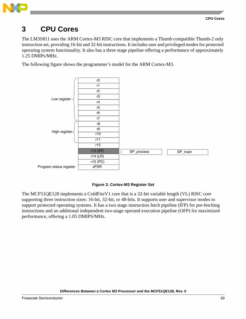
3 CPU CoresThe LM3S811 uses the ARM Cortex-M3 RISC core that implements a Thumb compatible Thumb-2 only instruction set, providing 16-bit and 32-bit instructions. It includes user and privileged modes for protected operating system functionality. It also has a three stage pipeline offering a performance of approximately 1.25 DMIPs/MHz.
The following figure shows the programmer’s model for the ARM Cortex-M3.
Figure 3. Cortex-M3 Register Set
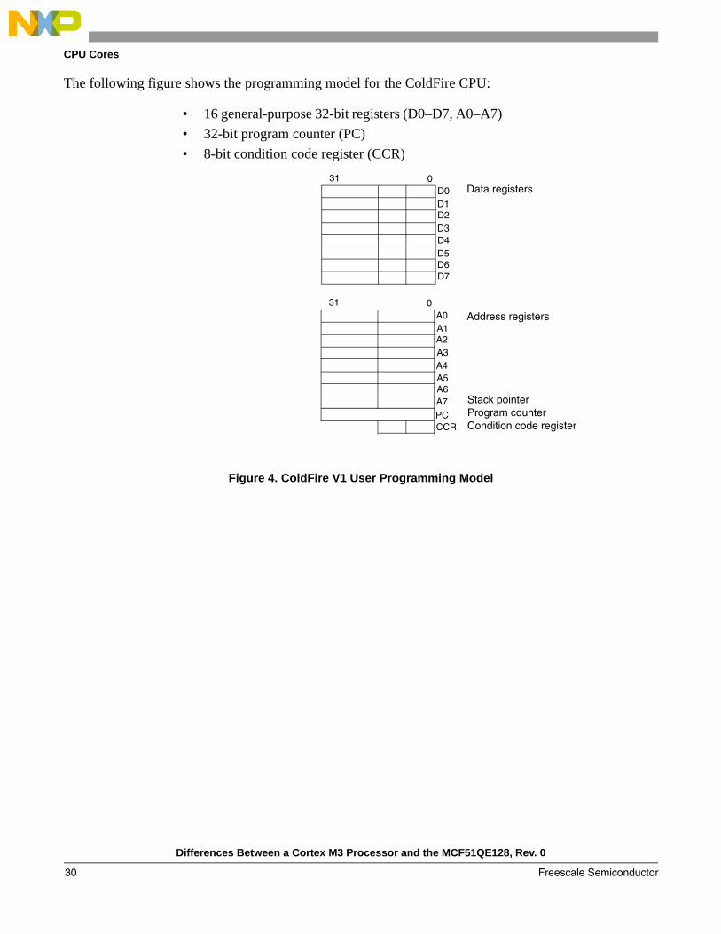
The MCF51QE128 implements a ColdFireV1 core that is a 32-bit variable length (VL) RISC core supporting three instruction sizes: 16-bit, 32-bit, or 48-bits. It supports user and supervisor modes to support protected operating systems. It has a two stage instruction fetch pipeline (IFP) for pre-fetching instructions and an additional independent two-stage operand execution pipeline (OFP) for maximized performance, offering a 1.05 DMIPS/MHz.
r0
r1
r2
r3
r4
r5
r7
r6
xPSR
r8
r10r9
r11
r13 (SP)
r12
r14 (LR)
r15 (PC)
SP_process SP_main
Low register
Program status register
High register
Differences Between a Cortex M3 Processor and the MCF51QE128, Rev. 0
Freescale Semiconductor 29
CPU Cores
The following figure shows the programming model for the ColdFire CPU:
Figure 4. ColdFire V1 User Programming Model
• 16 general-purpose 32-bit registers (D0–D7, A0–A7)• 32-bit program counter (PC)• 8-bit condition code register (CCR)
31
D1D2D3D4D5D6D7
0D0
31
A1A2A3A4A5A6A7
0A0
PCCCR
Data registers
Address registers
Stack pointerProgram counterCondition code register
Differences Between a Cortex M3 Processor and the MCF51QE128, Rev. 0
Freescale Semiconductor30
CPU Cores
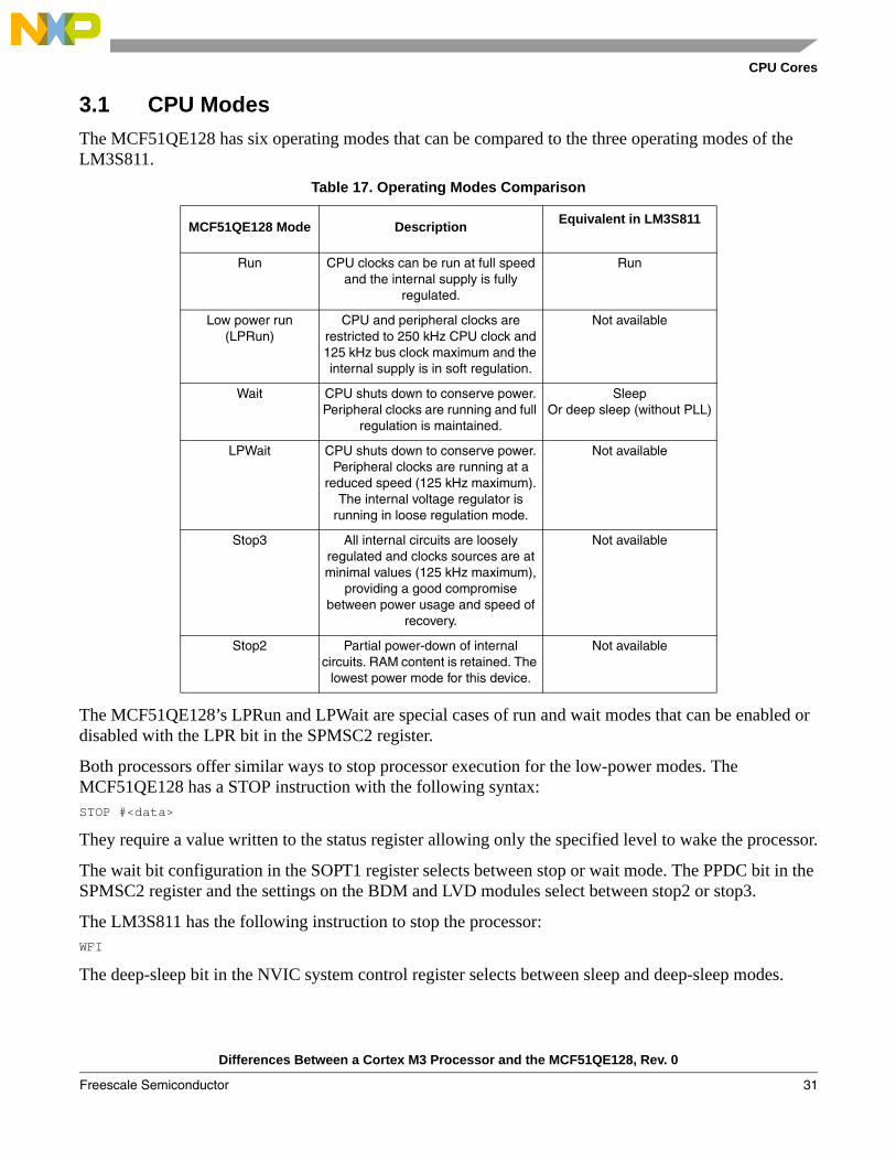
3.1 CPU ModesThe MCF51QE128 has six operating modes that can be compared to the three operating modes of the LM3S811.
The MCF51QE128’s LPRun and LPWait are special cases of run and wait modes that can be enabled or disabled with the LPR bit in the SPMSC2 register.
Both processors offer similar ways to stop processor execution for the low-power modes. The MCF51QE128 has a STOP instruction with the following syntax:STOP #<data>
They require a value written to the status register allowing only the specified level to wake the processor.
The wait bit configuration in the SOPT1 register selects between stop or wait mode. The PPDC bit in the SPMSC2 register and the settings on the BDM and LVD modules select between stop2 or stop3.
The LM3S811 has the following instruction to stop the processor:WFI
The deep-sleep bit in the NVIC system control register selects between sleep and deep-sleep modes.
Table 17. Operating Modes Comparison
MCF51QE128 Mode Description Equivalent in LM3S811
Run CPU clocks can be run at full speed and the internal supply is fully
regulated.
Run
Low power run (LPRun)
CPU and peripheral clocks are restricted to 250 kHz CPU clock and 125 kHz bus clock maximum and the internal supply is in soft regulation.
Not available
Wait CPU shuts down to conserve power. Peripheral clocks are running and full
regulation is maintained.
SleepOr deep sleep (without PLL)
LPWait CPU shuts down to conserve power. Peripheral clocks are running at a
reduced speed (125 kHz maximum). The internal voltage regulator is
running in loose regulation mode.
Not available
Stop3 All internal circuits are loosely regulated and clocks sources are at minimal values (125 kHz maximum),
providing a good compromise between power usage and speed of
recovery.
Not available
Stop2 Partial power-down of internal circuits. RAM content is retained. The
lowest power mode for this device.
Not available
Differences Between a Cortex M3 Processor and the MCF51QE128, Rev. 0
Freescale Semiconductor 31
CPU Cores
Any enabled interrupt can bring the LM3S811 out of both low power modes and the MCF51QE128 out of wait and LPWait.
A reset or the RTC, LVD/LVW, ADC, ACMP, IRQ, SCI, and KBI modules can bring the MCF51QE128 out of stop3. The RTC, IRQ, or RESET are the only paths out of stop2.
Section 4, “Power Consumption” compares the low power performance between both parts.
3.2 CPU PerformanceBenchmarking results depend on the type of application running and the C compiler efficiency. The following tests were performed as described in Section 5, “Software Considerations.”
3.2.1 Simple FunctionsThe following eleven basic functions were performed in both microcontrollers. These functions are encapsulated in the following form:return_param Function_name (param1, param2, …)
• They are completely C based and the same code runs in both parts• TwoCaseIf: Simple if-else statement• TenCaseIf: If-else if x10• FifteenCaseIf: If-else if x15• FifteenCaseSwitch: Switch statement with 15 cases• NoParamMethod: Execute empty function• Addition8: Add two 8-bit values (unsigned char) and return 8-bits• Addition32: Add two 32-bit values (unsigned long) and return 32-bits• Multiplication32: Multiply two 32-bit values (unsigned long) and return 32-bits• Division32: Divide two 32-bit values (unsigned long) and return 16-bits (unsigned short)• AdditionFloating: Add two floating point numbers (float) and return floating point• Forc1: For loop until 255
Differences Between a Cortex M3 Processor and the MCF51QE128, Rev. 0
Freescale Semiconductor32
CPU Cores
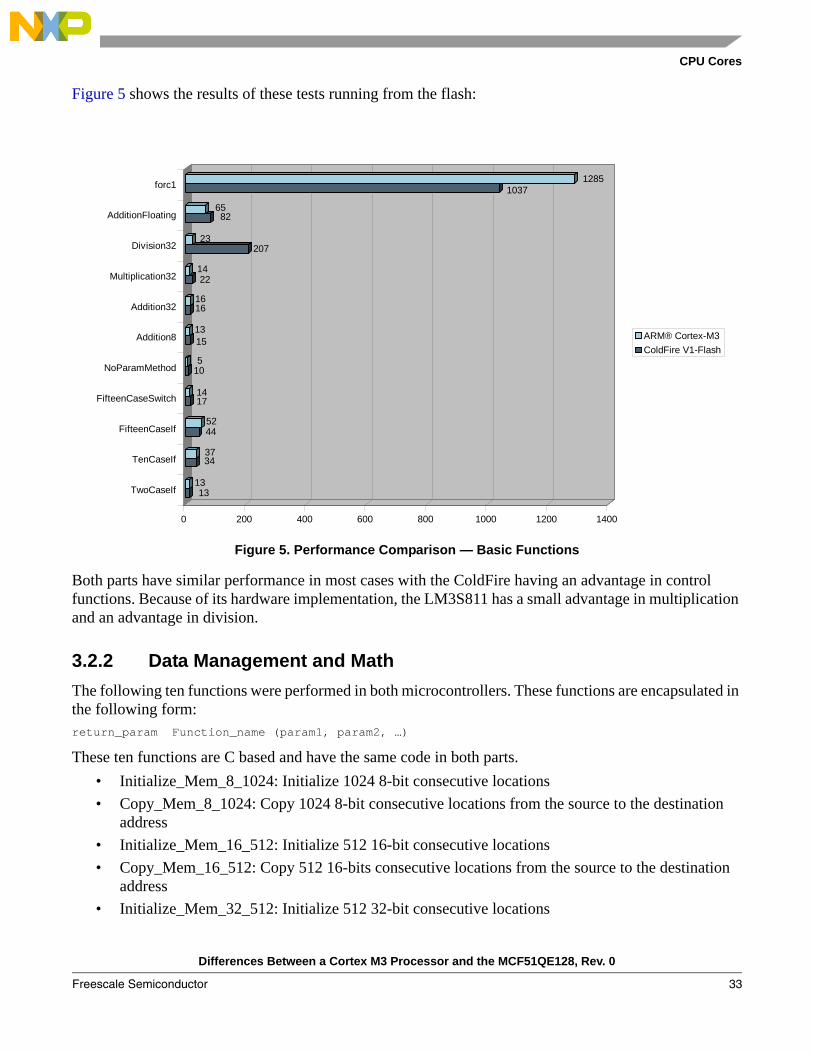
Figure 5 shows the results of these tests running from the flash:
Figure 5. Performance Comparison — Basic Functions
Both parts have similar performance in most cases with the ColdFire having an advantage in control functions. Because of its hardware implementation, the LM3S811 has a small advantage in multiplication and an advantage in division.
3.2.2 Data Management and MathThe following ten functions were performed in both microcontrollers. These functions are encapsulated in the following form:return_param Function_name (param1, param2, …)
These ten functions are C based and have the same code in both parts.• Initialize_Mem_8_1024: Initialize 1024 8-bit consecutive locations• Copy_Mem_8_1024: Copy 1024 8-bit consecutive locations from the source to the destination
address• Initialize_Mem_16_512: Initialize 512 16-bit consecutive locations• Copy_Mem_16_512: Copy 512 16-bits consecutive locations from the source to the destination
address• Initialize_Mem_32_512: Initialize 512 32-bit consecutive locations
1313
3437
4452
1714
105
1513
1616
2214
20723
8265
10371285
0 200 400 600 800 1000 1200 1400
TwoCaseIf
TenCaseIf
FifteenCaseIf
FifteenCaseSwitch
NoParamMethod
Addition8
Addition32
Multiplication32
Division32
AdditionFloating
forc1
ARM® Cortex-M3ColdFire V1-Flash
Differences Between a Cortex M3 Processor and the MCF51QE128, Rev. 0
Freescale Semiconductor 33
CPU Cores
• Copy_Mem_32_512: Copy 512 32-bits consecutive locations from the source to the destination address
• Average_8_256: Average 256 samples of 8-bit data• Average_16_1024: Average 1024 samples of 16-bit data• AddArray_32_256: Average 256 samples of 32-bit data• MultArrayxConst_16to32_512: Multiply one array of 512 16-bit data by a 16-bit constant and
return a 32-bit array.
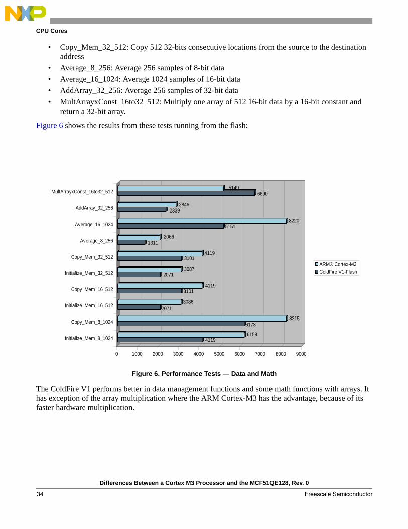
Figure 6 shows the results from these tests running from the flash:
Figure 6. Performance Tests — Data and Math
The ColdFire V1 performs better in data management functions and some math functions with arrays. It has exception of the array multiplication where the ARM Cortex-M3 has the advantage, because of its faster hardware multiplication.
41196158
61738215
20713086
31014119
20713087
31014119
13112066
51518220
23392846
66905149
0 1000 2000 3000 4000 5000 6000 7000 8000 9000
Initialize_Mem_8_1024
Copy_Mem_8_1024
Initialize_Mem_16_512
Copy_Mem_16_512
Initialize_Mem_32_512
Copy_Mem_32_512
Average_8_256
Average_16_1024
AddArray_32_256
MultArrayxConst_16to32_512
ARM® Cortex-M3ColdFire V1-Flash
Differences Between a Cortex M3 Processor and the MCF51QE128, Rev. 0
Freescale Semiconductor34
CPU Cores
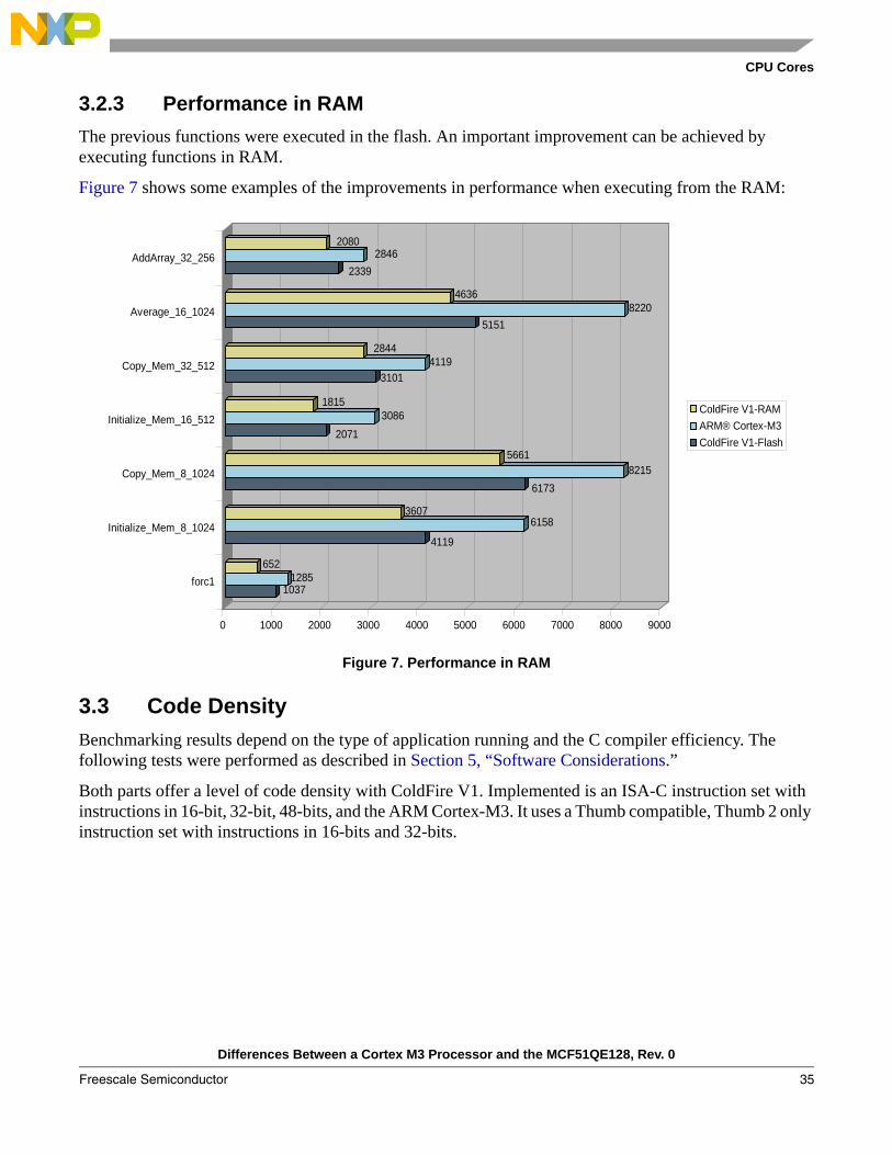
3.2.3 Performance in RAMThe previous functions were executed in the flash. An important improvement can be achieved by executing functions in RAM.
Figure 7 shows some examples of the improvements in performance when executing from the RAM:
Figure 7. Performance in RAM
3.3 Code DensityBenchmarking results depend on the type of application running and the C compiler efficiency. The following tests were performed as described in Section 5, “Software Considerations.”
Both parts offer a level of code density with ColdFire V1. Implemented is an ISA-C instruction set with instructions in 16-bit, 32-bit, 48-bits, and the ARM Cortex-M3. It uses a Thumb compatible, Thumb 2 only instruction set with instructions in 16-bits and 32-bits.
10371285
652
4119
61583607
61738215
5661
20713086
1815
31014119
2844
51518220
4636
23392846
2080
0 1000 2000 3000 4000 5000 6000 7000 8000 9000
forc1
Initialize_Mem_8_1024
Copy_Mem_8_1024
Initialize_Mem_16_512
Copy_Mem_32_512
Average_16_1024
AddArray_32_256
ColdFire V1-RAMARM® Cortex-M3ColdFire V1-Flash
Differences Between a Cortex M3 Processor and the MCF51QE128, Rev. 0
Freescale Semiconductor 35
CPU Cores
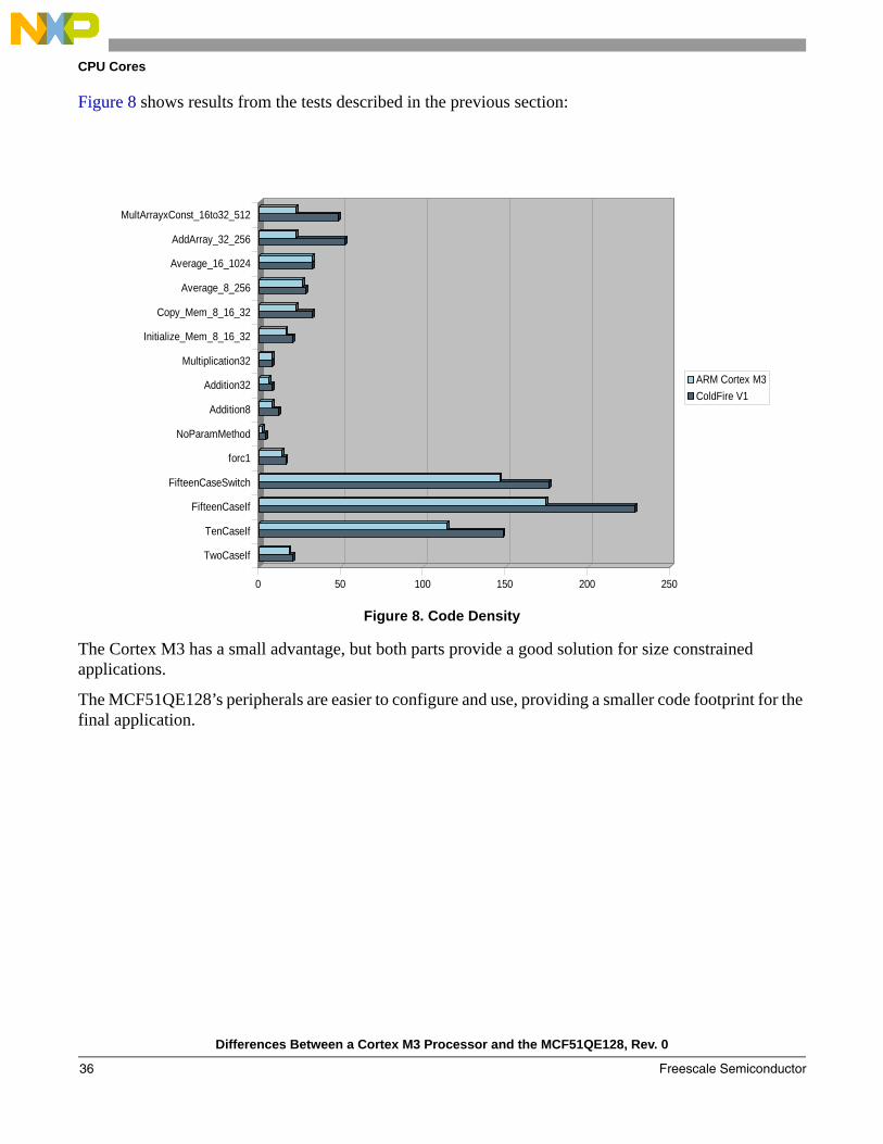
Figure 8 shows results from the tests described in the previous section:
Figure 8. Code Density
The Cortex M3 has a small advantage, but both parts provide a good solution for size constrained applications.
The MCF51QE128’s peripherals are easier to configure and use, providing a smaller code footprint for the final application.
0 50 100 150 200 250
TwoCaseIf
TenCaseIf
FifteenCaseIf
FifteenCaseSwitch
forc1
NoParamMethod
Addition8
Addition32
Multiplication32
Initialize_Mem_8_16_32
Copy_Mem_8_16_32
Average_8_256
Average_16_1024
AddArray_32_256
MultArrayxConst_16to32_512
ARM Cortex M3ColdFire V1
Differences Between a Cortex M3 Processor and the MCF51QE128, Rev. 0
Freescale Semiconductor36
Power Consumption
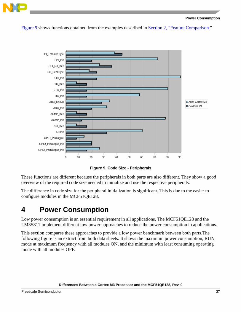
Figure 9 shows functions obtained from the examples described in Section 2, “Feature Comparison.”
Figure 9. Code Size - Peripherals
These functions are different because the peripherals in both parts are also different. They show a good overview of the required code size needed to initialize and use the respective peripherals.
The difference in code size for the peripheral initialization is significant. This is due to the easier to configure modules in the MCF51QE128.
4 Power ConsumptionLow power consumption is an essential requirement in all applications. The MCF51QE128 and the LM3S811 implement different low power approaches to reduce the power consumption in applications.
This section compares these approaches to provide a low power benchmark between both parts.The following figure is an extract from both data sheets. It shows the maximum power consumption, RUN mode at maximum frequency with all modules ON, and the minimum with least consuming operating mode with all modules OFF.
0 10 20 30 40 50 60 70 80 90
GPIO_PortOutput_Init
GPIO_PinOutput_Init
GPIO_PinToggle
KBIInit
KBI_ISR
ACMP_Init
ACMP_ISR
ADC_Init
ADC_Conv8
IIC_Init
RTC_Init
RTC_ISR
SCI_Init
Sci_SendByte
SCI_RX_ISR
SPI_Init
SPI_Transfer Byte
ARM Cortex M3ColdFire V1
Differences Between a Cortex M3 Processor and the MCF51QE128, Rev. 0
Freescale Semiconductor 37
Power Consumption
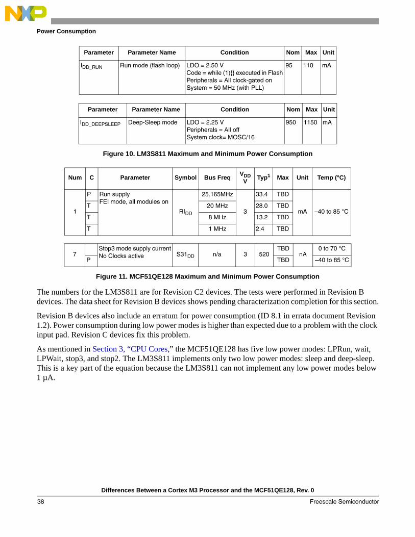
Figure 10. LM3S811 Maximum and Minimum Power Consumption
Figure 11. MCF51QE128 Maximum and Minimum Power Consumption
The numbers for the LM3S811 are for Revision C2 devices. The tests were performed in Revision B devices. The data sheet for Revision B devices shows pending characterization completion for this section.
Revision B devices also include an erratum for power consumption (ID 8.1 in errata document Revision 1.2). Power consumption during low power modes is higher than expected due to a problem with the clock input pad. Revision C devices fix this problem.
As mentioned in Section 3, “CPU Cores,” the MCF51QE128 has five low power modes: LPRun, wait, LPWait, stop3, and stop2. The LM3S811 implements only two low power modes: sleep and deep-sleep. This is a key part of the equation because the LM3S811 can not implement any low power modes below 1 µA.
Parameter Parameter Name Condition Nom Max Unit
IDD_RUN Run mode (flash loop) LDO = 2.50 VCode = while (1){} executed in FlashPeripherals = All clock-gated onSystem = 50 MHz (with PLL)
95 110 mA
Parameter Parameter Name Condition Nom Max Unit
IDD_DEEPSLEEP Deep-Sleep mode LDO = 2.25 VPeripherals = All offSystem clock= MOSC/16
950 1150 mA
Num C Parameter Symbol Bus Freq VDD V Typ1 Max Unit Temp (°C)
1
P Run supply FEI mode, all modules on
RIDD
25.165MHz
3
33.4 TBD
mA –40 to 85 °CT 20 MHz 28.0 TBD
T 8 MHz 13.2 TBD
T 1 MHz 2.4 TBD
7Stop3 mode supply currentNo Clocks active S31DD n/a 3 520
TBDnA
0 to 70 °C
P TBD –40 to 85 °C
Differences Between a Cortex M3 Processor and the MCF51QE128, Rev. 0
Freescale Semiconductor38
Power Consumption
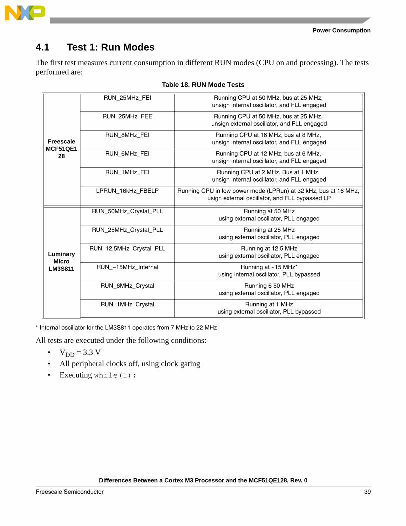
4.1 Test 1: Run ModesThe first test measures current consumption in different RUN modes (CPU on and processing). The tests performed are:
* Internal oscillator for the LM3S811 operates from 7 MHz to 22 MHz
All tests are executed under the following conditions:• VDD = 3.3 V• All peripheral clocks off, using clock gating• Executing while(1);
Table 18. RUN Mode Tests
Freescale MCF51QE1
28
RUN_25MHz_FEI Running CPU at 50 MHz, bus at 25 MHz, unsign internal oscillator, and FLL engaged
RUN_25MHz_FEE Running CPU at 50 MHz, bus at 25 MHz, unsign external oscillator, and FLL engaged
RUN_8MHz_FEI Running CPU at 16 MHz, bus at 8 MHz, unsign internal oscillator, and FLL engaged
RUN_6MHz_FEI Running CPU at 12 MHz, bus at 6 MHz, unsign internal oscillator, and FLL engaged
RUN_1MHz_FEI Running CPU at 2 MHz, Bus at 1 MHz, unsign internal oscillator, and FLL engaged
LPRUN_16kHz_FBELP Running CPU in low power mode (LPRun) at 32 kHz, bus at 16 MHz, usign external oscillator, and FLL bypassed LP
Luminary Micro
LM3S811
RUN_50MHz_Crystal_PLL Running at 50 MHzusing external oscillator, PLL engaged
RUN_25MHz_Crystal_PLL Running at 25 MHzusing external oscillator, PLL engaged
RUN_12.5MHz_Crystal_PLL Running at 12.5 MHzusing external oscillator, PLL engaged
RUN_~15MHz_Internal Running at ~15 MHz*using internal oscillator, PLL bypassed
RUN_6MHz_Crystal Running 6 50 MHzusing external oscillator, PLL engaged
RUN_1MHz_Crystal Running at 1 MHzusing external oscillator, PLL bypassed
Differences Between a Cortex M3 Processor and the MCF51QE128, Rev. 0
Freescale Semiconductor 39
Power Consumption
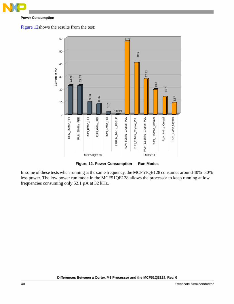
Figure 12shows the results from the test:
Figure 12. Power Consumption — Run Modes
In some of these tests when running at the same frequency, the MCF51QE128 consumes around 40%–80% less power. The low power run mode in the MCF51QE128 allows the processor to keep running at low frequencies consuming only 52.1 µA at 32 kHz.
22.7
5
22.7
3
9.63
8.26
1.81
0.0521
57.6
40.5
27.9
2
19.5
13.7
8
8.87
0
10
20
30
40
50
60
Cur
rent
in m
A
RU
N_2
5Mhz
_FE
I
RU
N_2
5Mhz
_FE
E
RU
N_8
Mhz
_FE
I
RU
N_6
Mhz
_FE
I
RU
N_1
Mhz
_FE
I
LPR
UN
_16K
hz_F
BE
LP
RU
N_5
0Mhz
_Cry
stal
_PLL
RU
N_2
5Mhz
_Cry
stal
_PLL
RU
N_1
2.5M
hz_C
ryst
al_P
LL
RU
N_~
15M
hz_I
nter
nal
RU
N_6
Mhz
_Cry
stal
RU
N_1
Mhz
_Cry
stal
MCF51QE128 LM3S811
Differences Between a Cortex M3 Processor and the MCF51QE128, Rev. 0
Freescale Semiconductor40
Power Consumption
4.2 Test 2: Low Power ModesThe following tests were performed to test the low power modes in both devices:
All tests are executed under the following conditions:• VDD = 3.3 V• All peripheral clocks are off except the ones mentioned in the above table.• CPU wakes on external event, falling edge.
Table 19. Low-Power Tests
Freescale MCF51QE1
28
WAIT_25MHz_FEI Wait mode. Bus at 25 MHz, using internal oscillator, FLL engaged andKBI enabled
STOP3 stop3 modeKBI enabled
STOP2 stop2 modeIRQ enabled
Luminary Micro
LM3S811
Sleep_50MHz_Crystal Sleep mode. Bus at 50 MHz,using external oscillator, PLL engaged andPTB enabled for external interrupt
Sleep_25MHz_Crystal Sleep mode. Bus at 25 MHz, PTB enabled for external interrupt
DeepSleep_Crystal Deep-sleep mode. Bus at 375 kHz, using external oscillator/16, PLL disabled andPTB enabled for external interrupt
Differences Between a Cortex M3 Processor and the MCF51QE128, Rev. 0
Freescale Semiconductor 41
Power Consumption
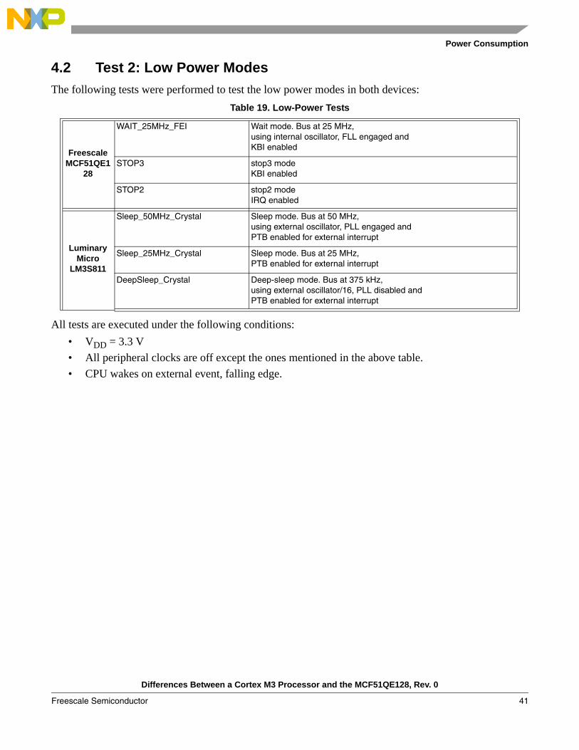
Figure 13shows the results from the test:
Figure 13. Power Consumption — Low-Power Modes
In wait mode vs. sleep mode the MCF51QE128 consumes ~¼ of the LM3S811’s power consumption. The MCF51QE128 includes three stop modes allowing power consumption below 1 µA. The LM3S811 does not include a similar functionality and its lowest power mode consumes around 1.5 mA.
The LM3S811 Revision B was used for these tests. There is a published errata for that mask (ID 8.1 in errata document Revision 1.2). According to the data sheet, the lowest power consumption is similar to DeepSleep_Crystal is around 1 mA.
4530
0.6 0.5
23670
16380
1570
0
5000
10000
15000
20000
25000
Cur
rent
in u
A
WA
IT_2
5Mhz
_FE
I
STO
P3
STO
P2
Sle
ep_5
0Mhz
_Cry
stal
Sle
ep_2
5Mhz
_Cry
stal
Dee
pSle
ep_C
ryst
al
MCF51QE128 LM3S811
Differences Between a Cortex M3 Processor and the MCF51QE128, Rev. 0
Freescale Semiconductor42
Power Consumption
4.3 Test 3: In ApplicationThe following test uses a periodic timer interrupt to read the ADC continuously.
The microcontrollers used the following configurations:
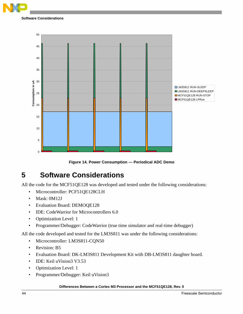
Figure 14 represents the different approaches:• Executing at the same frequency, the MCF51QE128 consumes ~50% less current than the
LM3S811. Added to the <1 µA stop modes, it can help achieve average power consumptions of less than 1mA or even below 1 µA, depending on the period.
• The low power run modes can achieve average current consumption below 100 µA without stopping the processor.
• The LM3S811 average current consumption is in the mA units or tens.
Table 20. ADC and Timer Test
Freescale MCF51QE128
MCF51QE128 RUN-STOP Run CPU at 50 MHz, bus at 25 MHz, and read ADC 23 mA
Go to stop3 with RTC using LPO 700 nA
MCF51QE128 LPRun Run CPU at 32 kHz, bus at 16 kHz with ADC, and RTC using LPO
253 uA
Run CPU at 32 kHz, bus at 16 kHz with RTC using LPO 52.1 µA
Luminary Micro
LM3S811
LM3S811 RUN-SLEEP Run CPU and bus at 25 MHz and read ADC 46.3 mA
Go to sleep mode with timer0 enabled 17.18 mA
LM3S811 RUN-DEEPSLEEP Run CPU and bus at 25 MHz and read ADC 46.3 mA
Go to deep-sleep mode with timer0 enabled 2.30 mA
Differences Between a Cortex M3 Processor and the MCF51QE128, Rev. 0
Freescale Semiconductor 43
Software Considerations
Figure 14. Power Consumption — Periodical ADC Demo
5 Software ConsiderationsAll the code for the MCF51QE128 was developed and tested under the following considerations:
• Microcontroller: PCF51QE128CLH• Mask: 0M12J• Evaluation Board: DEMOQE128• IDE: CodeWarrior for Microcontrollers 6.0• Optimization Level: 1• Programmer/Debugger: CodeWarrior (true time simulator and real-time debugger)
All the code developed and tested for the LM3S811 was under the following considerations:• Microcontroller: LM3S811-CQN50• Revision: B5• Evaluation Board: DK-LM3S811 Development Kit with DB-LM3S811 daughter board.• IDE: Keil uVision3 V3.53• Optimization Level: 1• Programmer/Debugger: Keil uVision3
0
5
10
15
20
25
30
35
40
45
50C
onsu
mpt
ion
in u
A
LM3S811 RUN-SLEEPLM3S811 RUN-DEEPSLEEPMCF51QE128 RUN-STOPMCF51QE128 LPRun
Differences Between a Cortex M3 Processor and the MCF51QE128, Rev. 0
Freescale Semiconductor44
Software Considerations
All the software used for performance and code density benchmarks were implemented from scratch using low-level accesses to registers. It discards additional overhead added by higher-level layers.
CodeWarrior includes an MCF51QE128.h file with definitions for all the registers, bits, and masks needed for the MCF51QE128. The ADCCFG register is shown for demonstration purposes. Below is a registered declaration example for the MCF51QE128:/*** ADCCFG - Configuration Register; 0xFFFF8016 ***/typedef union { byte Byte; struct { byte ADICLK0 :1; /* Input Clock Select Bit 0 */ byte ADICLK1 :1; /* Input Clock Select Bit 1 */ byte MODE0 :1; /* Conversion Mode Selection Bit 0 */ byte MODE1 :1; /* Conversion Mode Selection Bit 1 */ byte ADLSMP :1; /* Long Sample Time Configuration */ byte ADIV0 :1; /* Clock Divide Select Bit 0 */ byte ADIV1 :1; /* Clock Divide Select Bit 1 */ byte ADLPC :1; /* Low Power Configuration */ } Bits; struct { byte grpADICLK :2; byte grpMODE :2; byte :1; byte grpADIV :2; byte :1; } MergedBits;} ADCCFGSTR;extern volatile ADCCFGSTR _ADCCFG @0xFFFF8016;#define ADCCFG _ADCCFG.Byte#define ADCCFG_ADICLK0 _ADCCFG.Bits.ADICLK0#define ADCCFG_ADICLK1 _ADCCFG.Bits.ADICLK1#define ADCCFG_MODE0 _ADCCFG.Bits.MODE0#define ADCCFG_MODE1 _ADCCFG.Bits.MODE1#define ADCCFG_ADLSMP _ADCCFG.Bits.ADLSMP#define ADCCFG_ADIV0 _ADCCFG.Bits.ADIV0#define ADCCFG_ADIV1 _ADCCFG.Bits.ADIV1#define ADCCFG_ADLPC _ADCCFG.Bits.ADLPC#define ADCCFG_ADICLK _ADCCFG.MergedBits.grpADICLK#define ADCCFG_MODE _ADCCFG.MergedBits.grpMODE#define ADCCFG_ADIV _ADCCFG.MergedBits.grpADIV
#define ADCCFG_ADICLK0_MASK 1#define ADCCFG_ADICLK1_MASK 2#define ADCCFG_MODE0_MASK 4#define ADCCFG_MODE1_MASK 8#define ADCCFG_ADLSMP_MASK 16#define ADCCFG_ADIV0_MASK 32#define ADCCFG_ADIV1_MASK 64#define ADCCFG_ADLPC_MASK 128#define ADCCFG_ADICLK_MASK 3#define ADCCFG_ADICLK_BITNUM 0#define ADCCFG_MODE_MASK 12#define ADCCFG_MODE_BITNUM 2#define ADCCFG_ADIV_MASK 96#define ADCCFG_ADIV_BITNUM 5
Differences Between a Cortex M3 Processor and the MCF51QE128, Rev. 0
Freescale Semiconductor 45
Software Considerations
This register declaration makes the implementation easy by using these instructions:ADCCFG = 0x05; // 8-bit Access to registerADCCFG_ADLSMP = 1; // Bit access to registerADCCFG_MODE = 2; // Group access to register (2-bit in example)ADCCFG = ADCCFG_ADLSMP_MASK | ADCCFG_ADICLK0_MASK; // Use of masks for clearer code
The development environment for the LM3S811 uses an LM3Sxxxx.h file with definition for the different modules of the microcontroller included in addition, the header files.
These files include the offsets for each one of the registers following the next format. The ADCSSCTL0 register is used for demonstration purposes. Below is a registered definition for LM3S811://*************************************************************************// The following define the offsets of the ADC registers.//*************************************************************************… #define ADC_O_SSCTL0 0x00000044 // Sample sequence control 0 reg.…
//*************************************************************************//// The following define the bit fields in the ADC_SSCTL0, ADC_SSCTL1,// ADC_SSCTL2, and ADC_SSCTL3 registers. Not all fields are present in all// registers.//************************************************************************* #define ADC_SSCTL_TS7 0x80000000 // 8th temperature sensor select#define ADC_SSCTL_IE7 0x40000000 // 8th interrupt enable#define ADC_SSCTL_END7 0x20000000 // 8th sequence end select#define ADC_SSCTL_D7 0x10000000 // 8th differential select#define ADC_SSCTL_TS6 0x08000000 // 7th temperature sensor select#define ADC_SSCTL_IE6 0x04000000 // 7th interrupt enable#define ADC_SSCTL_END6 0x02000000 // 7th sequence end select…#define ADC_SSCTL_IE0 0x00000004 // 1st interrupt enable#define ADC_SSCTL_END0 0x00000002 // 1st sequence end select#define ADC_SSCTL_D0 0x00000001 // 1st differential select
This approach is useful for high level drivers. It handles the peripherals modularly, but it makes the low level implementation for register access more complex. It does not include bit or group definitions. Each location must be referenced with different offset levels, such as:*((unsigned long *) (ADC_BASE + ADC_O_SSCTL0)) = 0x06; // 8-bit access *((unsigned long *) (ADC_BASE + ADC_O_SSCTL0)) = ADC_SSCTL_IE0 | ADC_SSCTL_END0 ; // Using masks for clearer code
Both Freescale and Luminary Micro offer high-level drivers for their microcontrollers.
Luminary Micro offers the Stellaris® Peripheral Driver Library that includes a set of drivers for the peripherals included in the LM3S811 and their other ARM Cortex-M3 microcontrollers. These drivers allow an easier use of the peripherals by using higher level common language functions. Below are examples of LM3S811 Driver functions:void ComparatorConfigure (unsigned long ulBase, unsigned long ulComp, unsigned long ulConfig); void ADCIntEnable (unsigned long ulBase, unsigned long ulSequenceNum)
The function implementation is good in most cases, but some drivers do not exploit all the capabilities of the peripheral. This forces the user to write/modify the low-level code with the confusing register
Differences Between a Cortex M3 Processor and the MCF51QE128, Rev. 0
Freescale Semiconductor46
Software Considerations
declaration described above. Some functions become too complex to use, especially the initialization functions with many parameters to use.
CodeWarrior for the MCF51QE128 offers two solutions to allow faster and easier developments:• Device Initialization is fast, easy, and has a user-friendly way to configure and generate CPU
peripheral initialization code. It uses a graphical environment to guide the user during the device initialization.
• Processor Expert is a tool designed for rapid application development of embedded applications.
The peripherals can be initialized using common-language terminology, which is translated by the tool into C or assembly code accessing the required registers. This allows having the processor running and configured properly in less time.
By using embedded beans that provide hardware encapsulation in the form of a platform independent standard allows a faster initialization and a much faster development. This includes a set of functions that can be drag and dropped in your application.
The peripherals can be configured in a common language environment which is independent from the user code. This allows changes such as different pins or frequencies to be invisible for the user application.
Figure 15. Device Initialization
Differences Between a Cortex M3 Processor and the MCF51QE128, Rev. 0
Freescale Semiconductor 47
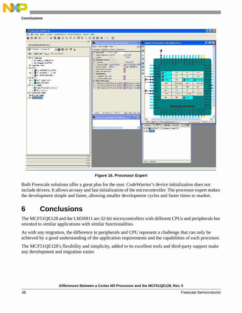
Conclusions
Figure 16. Processor Expert
Both Freescale solutions offer a great plus for the user. CodeWarrior’s device initialization does not include drivers. It allows an easy and fast initialization of the microcontroller. The processor expert makes the development simple and faster, allowing smaller development cycles and faster times to market.
6 ConclusionsThe MCF51QE128 and the LM3S811 are 32-bit microcontrollers with different CPUs and peripherals but oriented to similar applications with similar functionalities.
As with any migration, the difference in peripherals and CPU represent a challenge that can only be achieved by a good understanding of the application requirements and the capabilities of each processor.
The MCF51QE128’s flexibility and simplicity, added to its excellent tools and third-party support make any development and migration easier.
Differences Between a Cortex M3 Processor and the MCF51QE128, Rev. 0
Freescale Semiconductor48

THIS PAGE IS INTENTIONALLY BLANK
Differences Between a Cortex M3 Processor and the MCF51QE128, Rev. 0
Freescale Semiconductor 49
Document Number: AN3466Rev. 005/2008
How to Reach Us:
Home Page:www.freescale.com
Web Support:http://www.freescale.com/support
USA/Europe or Locations Not Listed:Freescale Semiconductor, Inc.Technical Information Center, EL5162100 East Elliot RoadTempe, Arizona 85284+1-800-521-6274 or +1-480-768-2130www.freescale.com/support
Europe, Middle East, and Africa:Freescale Halbleiter Deutschland GmbHTechnical Information CenterSchatzbogen 781829 Muenchen, Germany+44 1296 380 456 (English)+46 8 52200080 (English)+49 89 92103 559 (German)+33 1 69 35 48 48 (French)www.freescale.com/support
Japan:Freescale Semiconductor Japan Ltd.HeadquartersARCO Tower 15F1-8-1, Shimo-Meguro, Meguro-ku,Tokyo 153-0064Japan0120 191014 or +81 3 5437 [email protected]
Asia/Pacific:Freescale Semiconductor Hong Kong Ltd.Technical Information Center2 Dai King StreetTai Po Industrial EstateTai Po, N.T., Hong Kong+800 2666 [email protected]
For Literature Requests Only:Freescale Semiconductor Literature Distribution CenterP.O. Box 5405Denver, Colorado 802171-800-441-2447 or 303-675-2140Fax: [email protected]
Information in this document is provided solely to enable system and software implementers to use Freescale Semiconductor products. There are no express or implied copyright licenses granted hereunder to design or fabricate any integrated circuits or integrated circuits based on the information in this document.
Freescale Semiconductor reserves the right to make changes without further notice to any products herein. Freescale Semiconductor makes no warranty, representation or guarantee regarding the suitability of its products for any particular purpose, nor does Freescale Semiconductor assume any liability arising out of the application or use of any product or circuit, and specifically disclaims any and all liability, including without limitation consequential or incidental damages. “Typical” parameters that may be provided in Freescale Semiconductor data sheets and/or specifications can and do vary in different applications and actual performance may vary over time. All operating parameters, including “Typicals”, must be validated for each customer application by customer’s technical experts. Freescale Semiconductor does not convey any license under its patent rights nor the rights of others. Freescale Semiconductor products are not designed, intended, or authorized for use as components in systems intended for surgical implant into the body, or other applications intended to support or sustain life, or for any other application in which the failure of the Freescale Semiconductor product could create a situation where personal injury or death may occur. Should Buyer purchase or use Freescale Semiconductor products for any such unintended or unauthorized application, Buyer shall indemnify and hold Freescale Semiconductor and its officers, employees, subsidiaries, affiliates, and distributors harmless against all claims, costs, damages, and expenses, and reasonable attorney fees arising out of, directly or indirectly, any claim of personal injury or death associated with such unintended or unauthorized use, even if such claim alleges that Freescale Semiconductor was negligent regarding the design or manufacture of the part.
RoHS-compliant and/or Pb-free versions of Freescale products have the functionality and electrical characteristics as their non-RoHS-compliant and/or non-Pb-free counterparts. For further information, see http://www.freescale.com or contact your Freescale sales representative.
For information on Freescale’s Environmental Products program, go to http://www.freescale.com/epp.
Freescale™ and the Freescale logo are trademarks of Freescale Semiconductor, Inc. All other product or service names are the property of their respective owners.© Freescale Semiconductor, Inc. 2008. All rights reserved.