designing a hardware in the loop wireless digital channel...
TRANSCRIPT
Designing a Hardware in the Loop Wireless Digital Channel Emulator for Software Defined
Radio
Janarbek Matai, Pingfan Meng, Lingjuan Wu, Brad Weals, and Ryan Kastner
Department of Computer Science and Engineering,
University of California, San Diego
Toyon Research Corporation
December 11
FPT’2012
Motivation
Problem
Wireless system testing and verification Difficult
Current wireless system testing methods
Field testing Expensive, time consuming and difficult to repeat
Simulation limited by fidelity, excessive run time
2
Wireless Channel Emulator (WCE) Fills the gap left between simulation and field testing Repeatability, high-fidelity, and the opportunity to test complete
radio Software implementation is not feasible due to amount of
computation for large network
Background
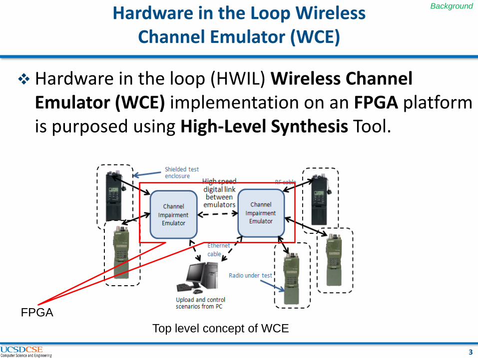
Hardware in the Loop Wireless Channel Emulator (WCE)
Hardware in the loop (HWIL) Wireless Channel
Emulator (WCE) implementation on an FPGA platform is purposed using High-Level Synthesis Tool.
3
Top level concept of WCE
FPGA
Background
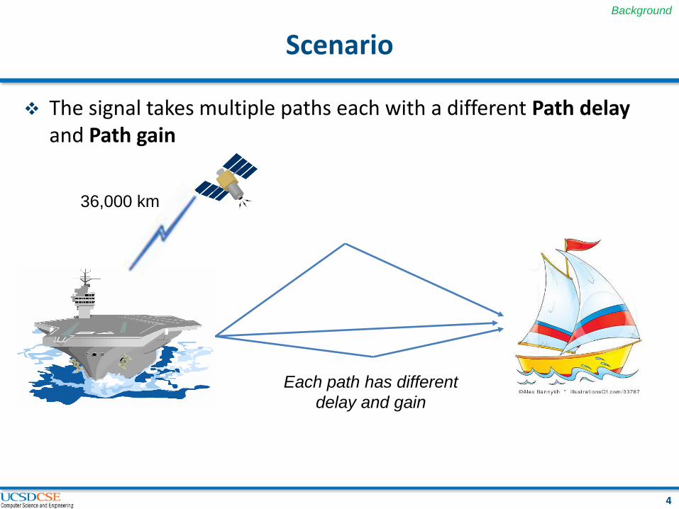
Scenario
The signal takes multiple paths each with a different Path delay and Path gain
4
36,000 km
Background
Each path has different
delay and gain
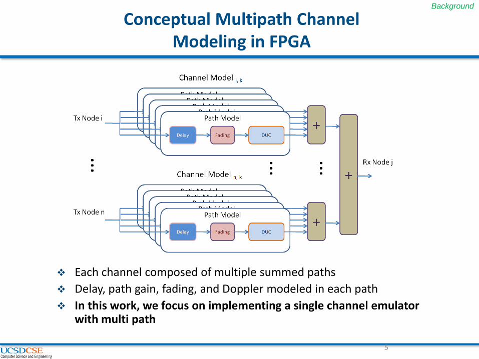
Conceptual Multipath Channel Modeling in FPGA
5
Each channel composed of multiple summed paths
Delay, path gain, fading, and Doppler modeled in each path
In this work, we focus on implementing a single channel emulator with multi path
Background
Single Channel Emulator Model
6
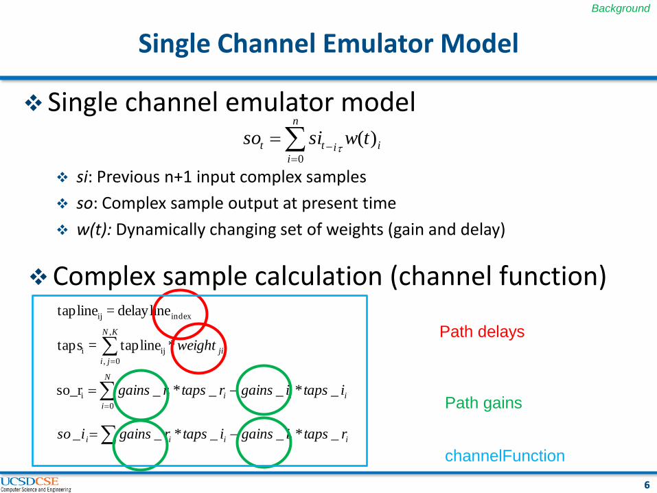
Single channel emulator model
si: Previous n+1 input complex samples
so: Complex sample output at present time
w(t): Dynamically changing set of weights (gain and delay)
6
i
n
iitt twsiso )(
0
iiiii
N
i
iiii
ji
KN
ji
rtapsigainsitapsrgainsiso
itapsigainsrtapsrgains
weight
_*__*__
_*__*_so_r
*tapline= taps
delayline = tapline
0
i
,
0,
iji
indexij
Complex sample calculation (channel function)
Path delays
Path gains
channelFunction
Background
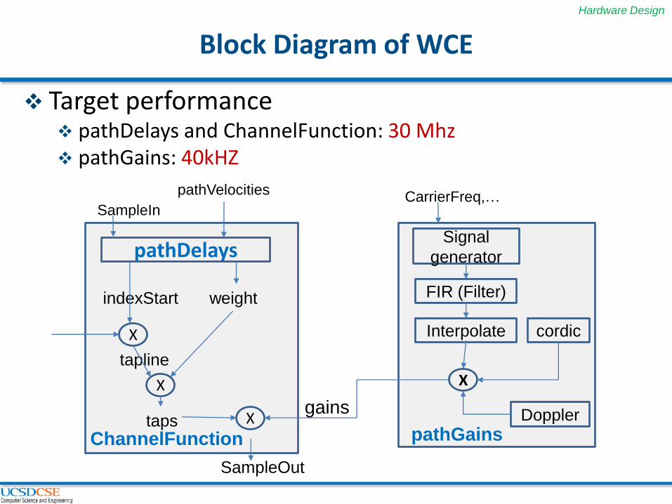
Block Diagram of WCE
SampleOut
pathDelays
pathVelocities
indexStart weight
X
tapline
X
taps X
SampleIn
ChannelFunction
gains
CarrierFreq,…
Signal
generator
FIR (Filter)
Interpolate cordic
Doppler
X
pathGains
Target performance pathDelays and ChannelFunction: 30 Mhz pathGains: 40kHZ
Hardware Design

High Level Synthesis
High Level Synthesis
Creates an RTL implementation from C level source code
Why use HLS ?
A good digital WCE has to handle wide range of dynamically changing parameters such as Doppler effect, fast fading, and multipath
HLS provides easy design space exploration with different parameters
E.g., varying number of paths in a channel
Script with Constraints
……………… ………………
VHDL Verilog
System C
HLS
Constraints/ Directives
………………
………………
C, C++, SystemC
RTL Synthesis
Courtesy to Xilinx
Hardware Design
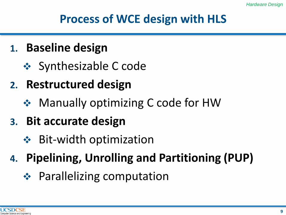
Process of WCE design with HLS
1. Baseline design
Synthesizable C code
2. Restructured design
Manually optimizing C code for HW
3. Bit accurate design
Bit-width optimization
4. Pipelining, Unrolling and Partitioning (PUP)
Parallelizing computation
9
Hardware Design
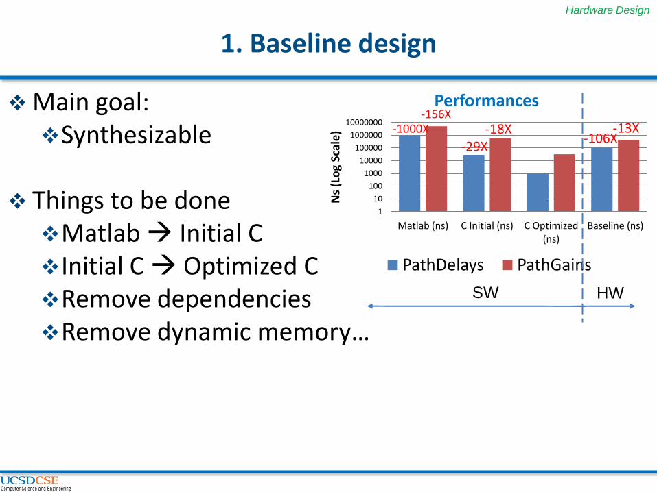
1. Baseline design
Main goal: Synthesizable
Things to be done Matlab Initial C Initial C Optimized C Remove dependencies Remove dynamic memory…
1
10
100
1000
10000
100000
1000000
10000000
Matlab (ns) C Initial (ns) C Optimized (ns)
Baseline (ns)
Ns
(Lo
g Sc
ale
)
Performances
PathDelays PathGains
-1000X
-29X -106X
-156X -18X -13X
Hardware Design
SW HW
1. Baseline - Results
11
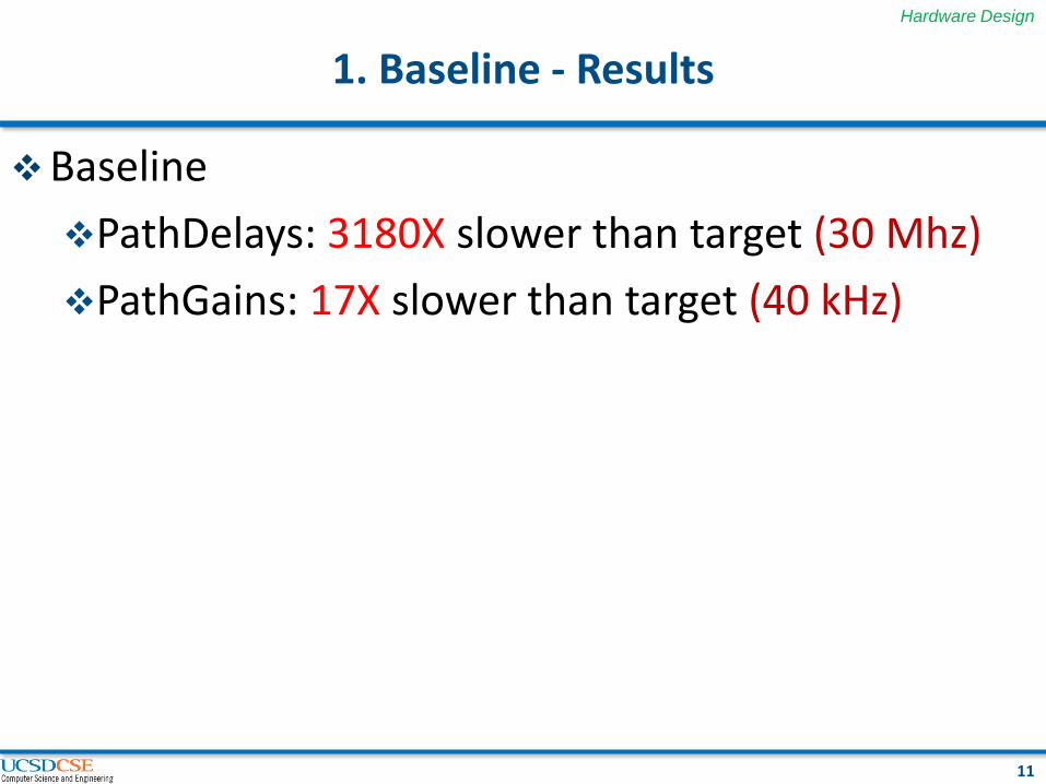
Baseline
PathDelays: 3180X slower than target (30 Mhz)
PathGains: 17X slower than target (40 kHz)
Hardware Design
2. Restructured Design
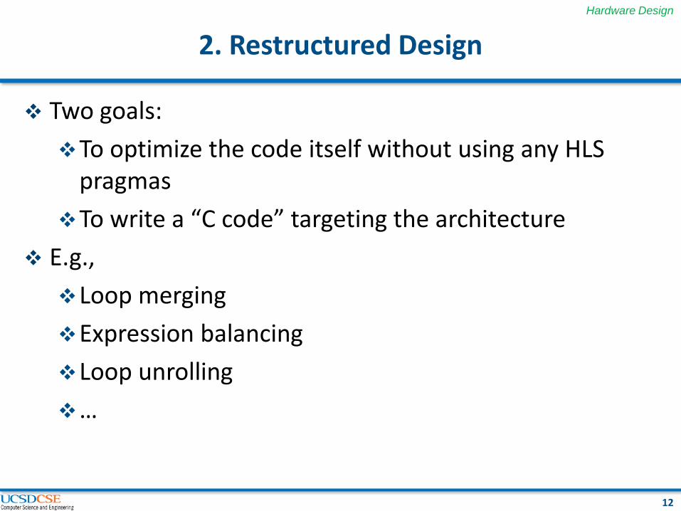
Two goals:
To optimize the code itself without using any HLS pragmas
To write a “C code” targeting the architecture
E.g.,
Loop merging
Expression balancing
Loop unrolling
…
12
Hardware Design
2. Restructured Design - Example
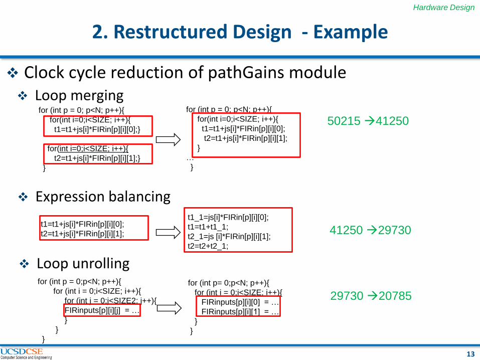
Loop merging
13
for (int p = 0;p<N; p++){
for (int i = 0;i<SIZE; i++){
for (int j = 0;j<SIZE2; j++){
FIRinputs[p][i][j] = …
}
}
}
for (int p= 0;p<N; p++){
for (int i = 0;i<SIZE; i++){
FIRinputs[p][i][0] = …
FIRinputs[p][i][1] = …
}
}
for (int p = 0; p<N; p++){
for(int i=0;i<SIZE; i++){
t1=t1+js[i]*FIRin[p][i][0];}
for(int i=0;i<SIZE; i++){
t2=t1+js[i]*FIRin[p][i][1];}
}
for (int p = 0; p<N; p++){
for(int i=0;i<SIZE; i++){
t1=t1+js[i]*FIRin[p][i][0];
t2=t1+js[i]*FIRin[p][i][1];
}
…
}
t1=t1+js[i]*FIRin[p][i][0];
t2=t1+js[i]*FIRin[p][i][1];
t1_1=js[i]*FIRin[p][i][0];
t1=t1+t1_1;
t2_1=js [i]*FIRin[p][i][1];
t2=t2+t2_1;
Expression balancing
Loop unrolling
41250 29730
50215 41250
29730 20785
Clock cycle reduction of pathGains module
Hardware Design

14
2. Restructured Design – Results
Restructured design vs. Target
PathDelays: 523X slower than target (30 Mhz)
PathGains: 7X slower than target (40 kHz)
ChannelFunction: 229X slower than target (30 Mhz)
Hardware Design
3. Bit accurate design
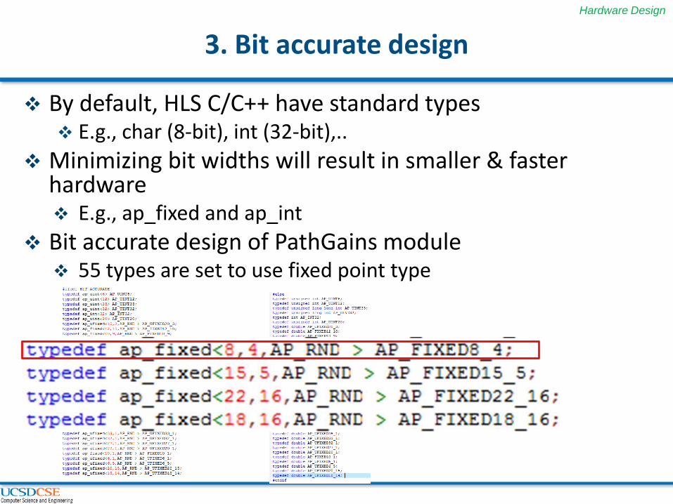
By default, HLS C/C++ have standard types E.g., char (8-bit), int (32-bit),..
Minimizing bit widths will result in smaller & faster hardware E.g., ap_fixed and ap_int
Bit accurate design of PathGains module 55 types are set to use fixed point type
Hardware Design
3. Bit accurate design - Results
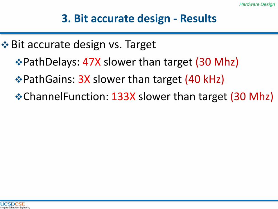
Bit accurate design vs. Target
PathDelays: 47X slower than target (30 Mhz)
PathGains: 3X slower than target (40 kHz)
ChannelFunction: 133X slower than target (30 Mhz)
Hardware Design

4. Pipelining and Partitioning
On top of bit accurate design, PUP is applied
Pipeline
Improves throughput
Default: Target initiation interval(II) of 1 II=2,II=3,…
Partition
BRAMs limit pipelining Partition large BRAMs into smaller BRAMS or into registers
17
Hardware Design

4. Pipelining and Partitioning - Example
pathDelays Optimizations: Partition: 5 BRAM, Pipeline: II=1 DSP48: 1930 (57%), FF: 424786 (85%), LUT: 5634230 (651%) Throughput: 47X than bit accurate design
pathGains Optimizations: Partition: 12 BRAM of 42, Pipeline/Unroll DSP48E: 4786 (82%), FF: 2039934421 (68%), LUT: 2212138893 (75%) Throughput: 15X than bit accurate design
18
Hardware Design
4. Pipelining and Partitioning -Results
19
Hardware Design
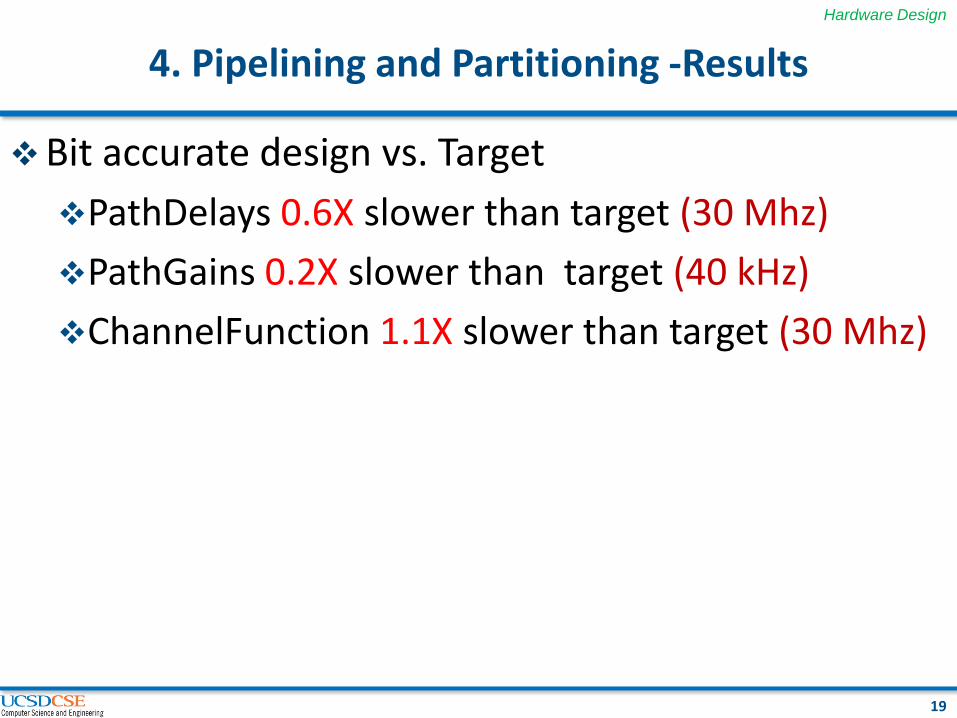
Bit accurate design vs. Target
PathDelays 0.6X slower than target (30 Mhz)
PathGains 0.2X slower than target (40 kHz)
ChannelFunction 1.1X slower than target (30 Mhz)
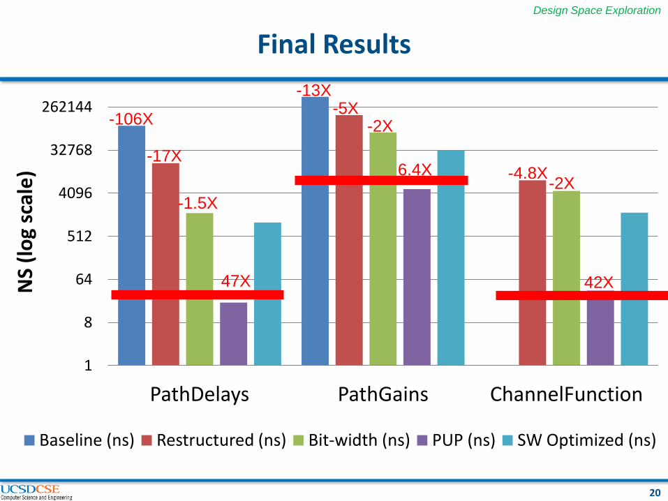
Final Results
20
1
8
64
512
4096
32768
262144
PathDelays PathGains ChannelFunction
NS
(lo
g sc
ale
)
Baseline (ns) Restructured (ns) Bit-width (ns) PUP (ns) SW Optimized (ns)
47X
-1.5X
-106X
-17X
-13X -5X
-2X
6.4X -4.8X -2X
42X
Design Space Exploration
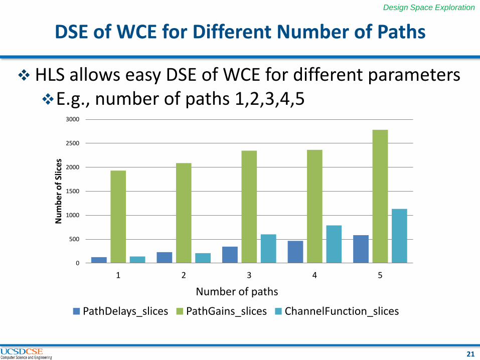
DSE of WCE for Different Number of Paths
HLS allows easy DSE of WCE for different parameters E.g., number of paths 1,2,3,4,5
21
0
500
1000
1500
2000
2500
3000
1 2 3 4 5
Nu
mb
er
of
Slic
es
Number of paths
PathDelays_slices PathGains_slices ChannelFunction_slices
Design Space Exploration

Results for Five Paths
Slices LUT FF DSP48E BRAM
PathDelays 584 1843 411 30 0
PathGains 2783 8756 7044 53 30
ChannelFunction 1131 3469 1798 40 0
22
Clock Cycles
Clock Period (ns)/ Frequency Latency(ns)/Throughput
PathDelays 4 5.394 /184 Mhz 21 / 47 Mhz
PathGains 501 9.97 / 100 Mhz 4994 /0.2 Mhz
ChannelFunction 6 6.62 /151 Mhz 37 /26 Mhz
Resource (xc6vlx240t)
Performance
Results

Design Effort
23
Design Days spend Tasks
Baseline 25.9% (28 hours) Understanding the code Converting matlab to C++, Removing library dependency, Writing HLS synthesizable code
Restructured code 22.2% (24 hours) Manually loop merging, Expression balancing, Loop unrolling
Bit Accurate Design 29.6% (32 hours) Calculation of 57 fixed point type widths (pathGains: 36, PathDelays:19, ChannelFunction: 2)
Optimized Design 7.4% (8 hours) Optimizing using directives
Collecting Results/DSE/Presenting
14.8% (16 hours) DSE, Collecting results, Presenting
Total ~108 hours
Conclusion
Designed single channel wireless emulator using HLS tool.
HLS provides easy parameterization of WCE design.
We plan to extend this work to multiple channel emulator and make end-to-end system
Lessons Learned
Achieving target performance and area depends
Writing a “C Code” targeting architecture is essential
Application and code size
2 optimization pragmas (pipeline, partition out of 33) + Restructured code+ Bit Width Target goal
24