design principles for single loop transistor feedback amplifiers
TRANSCRIPT

1957 IRE TRANSACTIONS ON CIRCUIT THEORY
Design Principles for Single Loop Transistor Feedback Amplifiers*
FRANKLIN H. BLECHERt
I. INTRODUCTION
HIS PAPER considers the design of single loop transistor feedback amplifiers. A criterion of stability is introduced which is useful for either
calculating or measuring the stability margins of transistor amplifiers, and in particular, single loop feedback ampli- fiers. Expressions are derived for relating sensitivity and impedance to feedback. Practical design techniques are discussed and are illustrated by the design of a I-mc carrier-frequency feedback amplifier. One of the important ideas expounded is that a transistor feedback amplifier is an excellent wide-band video amplifier. Because of the transit time cutoff in junction transistors, it is necessary to sacrifice low-frequency gain in order to broadband an amplifier. The best method for accomplishing this is to use negative feedback. When properly designed, the gain of the amplifier is essentially independent of the low- frequency transistor gain, and the useful bandwidth is competitive with that obtained with other design methods.le3
II. RETURN DIFFERENCE, RETURN RATIO, AND LOOP CURRENT TRANSMISSION
In order to place the design of transistor feedback amplifiers on a sound basis, it is necessary to have a rigorous criterion of stability. The concept of return .difference” which has proven extremely useful for vacuum %ube amplifiers is also applicable to transistors. A method .of calculating or measuring the return difference for a -transistor in either the common base or the common .emitter connection will be described.5 Before this dis- cussion, it is necessary to examine the equivalent circuit ~of the transistor. Fig. 1 shows equivalent circuits for the transistor in the common base and common emitter .connections, respectively.6 The device parameter a is zomplex and has a dc value equal to a, (very nearly equal to unity) and has a magnit,ude of 0.707~~ at the radian
* Manuscript received by the PGCT, May 1, 1957. t Bell Telephone Labs., Inc., Murray Hill, N. J. 1 J. G. Linvill and L. G. Schimpf, “The design of tetrode transis-
-tar amplifiers,” Bell Sys. Tech. J., vol. 35, pp. 813-840; July, 1956. *J. F. Gibbons, “The Design of Alignable Transistor Ampli-
fiers,” Tech. Rep. No. 106, Stanford Electronics Lab., Stanford, ,Calif.; May 7, 1956.
3 G. Bruun, “Common-emitt.er transistor video amplifiers,” PROC. IRE, vol. 44, pp. 1561-1572; November, 1956.
4 H. W. Bode, “Network Analysis and Feedback Amplifier De- :sign,” D. Van Nostrand Co.., Inc., New York, N. Y., ch. 4; 1945.
5 In principle, the analysis can be applied to a transistor in the common collector connection, but it is somewhat cumbersome.
6 For a good description of transistor equivalent circuits see .R. L. Pritchard, “Electric network representation of transistors-a .survey,” IRE TRANS., vol. CT-3, pp. 5-21; March, 1956.
145
(4
.,_--_-__ ” -.+b- ____ --_-_-_----- --------- -L I ,I I CbC 1
(b)
a& -(Ll/w.)m a= 1 2, = rc
lf” 1 + pr,c,
0.8 ce = ;
a e 2, = re
1 + pr,c,
p = jw Fig. l-(a) Common base equivalent circuit, (b) common emitter
equivalent circuit.
frequency u..’ The phase shift of the parameter a exceeds the phase shift associated with an RC cutoff by m radians at the frequency u,. In the case of an ideal one-dimen- sional junction transistor (one in which .the minority carriers in the base region move only by diffusion) the ,excess phase shift at w, is 0.21 radians (129.’ High- frequency types of transistors, particularly drift and diffused-base junction transistors, have considerably more excess phase because of an electric field in the base region, and the effect of emitter depletion layer capacity. This excess phase must be taken into account when designing feedback amplifiers.
With reference to Fig. 1, r, is the collector resistance, C, is the collector capacity, r, is the emitter resistance, C. is approximately the emitter storage capacity, pcL,,’ is
7 The radian frequency w. is very nearly equal to the alpha-cut- off frequency, the frequency at which the current gain of a common base stage is 3 db down.
8 R. 1,. Pritchard, “Frequency variations of current-amplification factor for junction transistors,” November, 1952.
PROC. IRE, vol. 40, pp. 1476-1481;
9 J. M. Early, “Effects of space charge layer widening in junc- tion transistors,” PROC. IRE, vol. 40, pp. 1401-1405; November, 1952.
146 IRE TRANSACTIONS ON CIRCUIT THEORY September
the inherent voltage feedback ratio, and r; is the ohmic base spreading resistance. To a good approximation, these device parameters are independent of frequency except for r;. It has been shown” that for grown junction transistors, r; has to be replaced at high frequencies by a complex frequency dependent impedance. However, with the above parameters assumed constant, very good agreement with experiment is obtained for frequencies between dc and w,.
In the case of grown junction transistors it is usually necessary to add a resistance (in the order of 100 ohms) in series with the collector junction due to collector body resistance. In the case of diffused base transistors it is necessary to add a resistance in series with the collector junction and a resistance in series with the emitter junc- tion to take account’ of body and contact resistances.
Due to parasitic capacitances introduced by the transistor header, socket, and circuit miring, the equiv- alent circuits must be modified by adding capacitors Cbc, Cbc, and C,,. In the case of the common base con- nection, C,,* and Cbc shunt the input and output circuits, respectively, and C,, introduces feedback. Similarly for the common emitter connection, Ca. and C,, shunt the input and output circuits, respectively, and Cbc introduces feedback. In this paper, the parasitic input and output capacitances will be lumped with the terminal networks, while the feedback capacitance mill be treated as an additional external feedback connection.
From the common base equivalent circuit it is evident that the forward transmission is partly due to the active part of the device, uZeic, and partly due to the passive part, ri. Consequently, if the active part of the device is set equal to zero, there is still a residual forward trans- mission due to ri. The transistor has internal feedback, due to r: and the voltage generator ~.,v,‘. Similar remarks can be made for the transistor in the common emitter configuration. Strictly speaking then, a single loop transistor feedback amplifier (one external feedback connection) is really a multiple loop feedback amplifier due to the internal feedback in each transistor. The criterion of stability must take into account both the residual passive transmission in the transistor and its internal feedback.
In order to simplify the.discussion, the inherent voltage feedback ratio, pet, will be assumed equal to zero. This is a legitimate assumption at high frequenciesll where the internal feedback provided by P.= is negligible compared to the effect of r;, but is a poor assumption at low fre- quencies. In Appendix I, the analysis is extended to take into account the effect of pL,,.
The return difference for a transistor in the common base connection is defined as equal to
ia R. IL Pritchard, “Theory of grown-junction transistor at high frequencies,” presented at Semiconductor Device Res. Conf., Min- neapolis, Minn.; June, 1954.
11 It is shown in Appendix I that the effect of pee.. is negligible at frequencies for which rb’;// 2, 1 > pee for the common base connec- tion, and 1 2. //I Z&l - a) 1 >> prc for the common emitter connec- tion.
AMPLIFIER EXCLUSIVE OF COMMON BASE
STAGE IN OUESTION
N
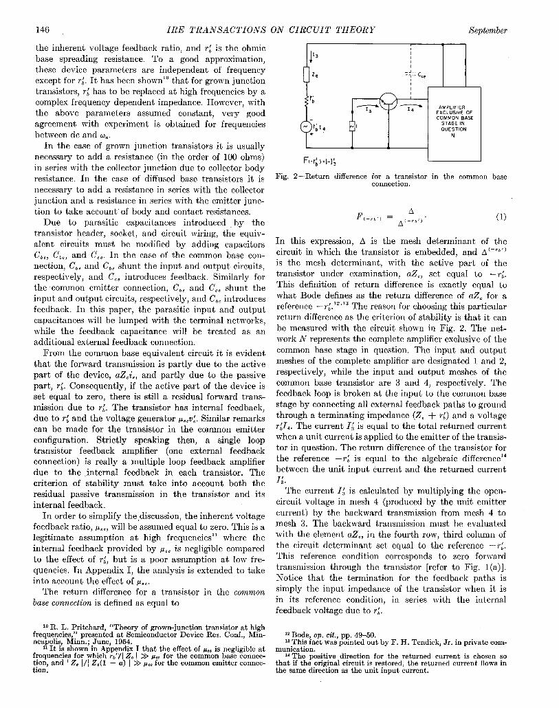
FM;, I q-1;
Fig. a-Return difference for a transistor in the common base connection.
In this expression, A is the mesh determinant of the circuit in which the transistor is embedded, and A’-“” is the mesh determinant, with the active part of the transistor under examination, aZ,, set equal to -r;. This definition of return difference is exactly equal to what Bode defines as the return difference of aZ, for a reference ---T~.~“~’ The reason for choosing this particular return difference as the criterion of stability is that it can be measured with the circuit shown in Fig. 2. The net- work N represents the complete amplifier exclusive of the common base stage in question. The input and output meshes of the complete amplifier are designated 1 and 2, respectively, while the input and output meshes of the common base transistor are 3 and 4, respectively. The feedback loop is broken at the input to the common base stage by connecting all external feedback paths to ground through a terminating impedance (2. + Y-L) and a voltage r:l,. The current 1; is equal to the total returned current when a unit current is applied to the emitter of the transis- tor in question. The return difference of the transistor for the reference -rL is equal to the algebraic differenceI between the unit input current and the returned current I;.
The current 1; is calculated by multiplying the open- circuit voltage in mesh 4 (produced by the unit emitter current) by the backward transmission from mesh 4 to mesh 3. The backward transmission must be evaluated with the element aZ,, in the fourth row, third column of the circuit determinant set equal to the reference -ri. This reference condition corresponds to zero forward transmission through the transistor [refer to Fig. l(a)]. Notice that the termination for the feedback paths is simply the input impedance of the t,ransistor when it is in its reference condition, in series with the internal feedback voltage due to r;.
I2 Bode, op. cit., pp. 49-50. I3 This fact was pointed out by F. H. Tendick, Jr. in private com-
munication. I4 The positive direction for the returned current is chosen so
that if the original circuit is restored, the returned current flows in the same direction as the unit input current.
1957 Blecher: Transistor Feedback BmpliJiers
(2)
where Ak3 is a minor of the circuit determinant (fourth row, third column deleted).
F(--rb’, = l _ Ij = 1 + (r,’ + aZJA43 A(-rb’)
(3)
A F<...,,,, = -. A(-rb’) (1)
An amplifier is stable if the zeros of A are restricted to the left half of the complex frequency plane. In order to determine if any zeros of A lie in the right half of the complex frequency plane me will use the following funda- mental theorem.15
Theorem: If a function X(p) is analytic except for possible poles within the right half of the complex fre- quency plane and approaches a finite fixed value as the magnitude of p approaches infinity, then the number of times the plot of S(p) encircles the origin of the X(p) plane in the clockwise direction while p itself moves from p = - jco to p = ja along the real frequency axis, is equal to the number of zeros of S(p) lying in the right half plane diminished by the number of poles of S(p) within the right half plane, when each zero and pole is counted in accordance with its multiplicity.
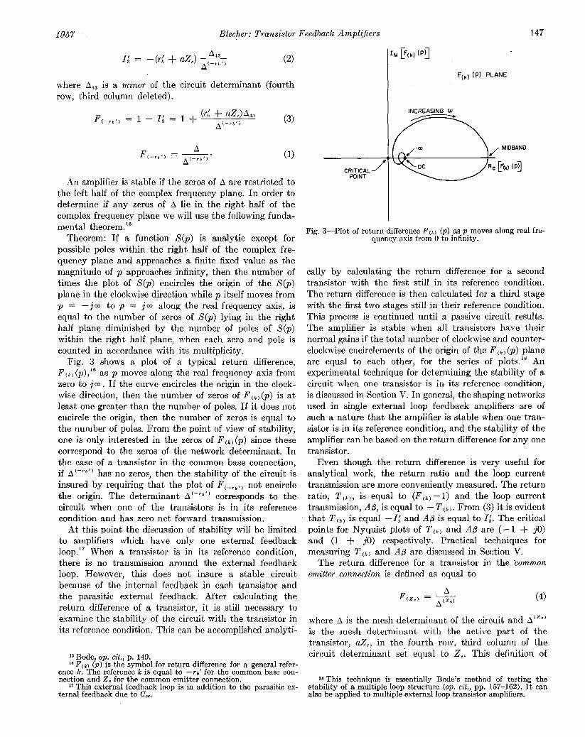
Fig. 3 shows a plot of a typical return difference, Fw, (P),‘” as p moves along the real frequency axis from zero to jm . If the curve encircles the origin in the clock- wise direction, then the number of zeros of F Ck) (p) is at least one greater than the number of poles. If it does not encircle the origin, then the number of zeros is equal to the number of poles. From the point of view of stability, one is only interested in the zeros of F Ckl (p) since these correspond to the zeros of the network determinant. In the case of a transistor in the common base connection, if A (-rb’) has no zeros, then the stability of the circuit is insured by requiring that the plot of FC-,,,, not encircle the origin. The determinant A(-‘*‘) corresponds to the circuit when one of the transistors is in its reference condition and has zero net forward transmission.
At this point the discussion of stability will be limited to amplifiers which have only one external feedback loop.” When a transistor is in its reference condition, there is no transmission around the external feedback loop. However, this does not insure a stable circuit because of the internal feedback in each transistor and the parasitic external feedback. After calculating the return difference of a transistor, it is still necessary to examine the stability of the circuit with the transistor in its reference condition. This can be accomplished analyti-
I5 Rod? op.. cit., p. 149. I6 F(k) p) 1s the symbol for return difference for a general refer-
ence lc. The reference k is equal to -rb’ for the common base con- nection and 2, for the common emit,ter connection.
I7 This external feedback loop is in addition to the parasitic ex- ternal feedback due to C,,.
CRITICAL / POINT
F(,) (PI PLANE
INCREASING W
Fig. a--Plot of return difference Fck) (p) as p moves along real fre- quency Sxis from 0 to infinity.
tally by calculating the return difference for a second transistor with the first still in its reference condition. The return difference is then calculated for a third stage with the first two stages still in their reference condition. This process is continued until a passive circuit results. The amplifier is stable when all transistors have their normal gains if the total number of clockwise and counter- clockwise encirclements of the origin of the F CkJ (p) plane are equal to each other, for the series of plots.” An experimental technique for determining the stability of a circuit when one transistor is in its reference condition, is discussed in Section V. In general, the shaping networks used in single external loop feedback amplifiers are of such a nature that the amplifier is stable when one tran- sistor is in its reference condition, and the stability of the amplifier can be based on the return difference for any one transistor.
Even though the return difference is very useful for analytical work, the return ratio and the loop current transmission are more conveniently measured. The return ratio, T Ckj, is equal to (FCkj -1) and the loop current transmission, A@, is equal to - T Ck). From (3) it is evident that TCkj is equal -I,’ and A@ is equal to I;. The critical points for Nyquist plots of T Ck) and AP are (- 1 + j0) and (1 + j0) respectively. Practical techniques for measuring T Ckl and A/3 are discussed in Section V.
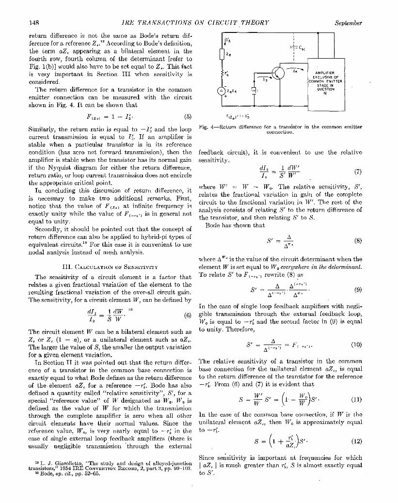
The return difference for a transistor in the ‘common emitter connection is defined as equal to
F A
(2.1 = - A (Z.1 (4)
where A is the mesh determinant of the circuit and A’“” is the mesh determinant with the active part of the transistor, a.??,, in the fourth row, third column of the circuit determinant se’t equal to 2,. This definition of
18 This technique is essentially Bode’s method of testing the stability of a multiple loop structure (op. cit., pp. 157-162). It can also be applied to multiple external loop transisbor amplifiers.
148 IRE TRANSACTIONS ON CIRCUIT THEORY
return difference is not the same as Bode’s return dif- ference for a reference Z,.” According to Bode’s definition,
I’ l3
the term ~2, appearing as a bilateral element in the
September
fourth row, fourth column of the determinant [refer to Fig. l(b)] would also have to be set equal to 2.. This fact is very important in Section III when sensitivity is considered.
I
AMPLIFIER EXCLUSIVE OF
COMMON EMITTER STAGE IN
The return difference for a transistor in the common emitter connection can be measured with the circuit shown in Fig. 4. It can be shown that
Fc,,, = 1 - I:- (5)
OUESTION N
FQ I - 1;
Similarly, the return ratio is equal to -1; and the loop current transmission is equal to 1;. If an amplifier is stable when a particular transistor is in its reference condition (has zero net forward transmission), then the amplifier is stable when the transistor has its normal gain if the Nyquist diagram for either the return difference, return ratio, or loop current transmission does not encircle the appropriate critical point.
In concluding this discussion of return difference, it is necessary to make two additional remarks. First, notice that the value of F(,,, at infinite frequency is exactly unity while the value of F C--rl,j is in general not equal to unity.
Secondly, it should be pointed out that the concept of return difference can also be applied to hybrid-pi types of equivalent circuits.l’ For this case it is convenient to use nodal analysis instead of mesh analysis.
III. CALCULATIC)N OF SENSITIVITY
The sensitivity of a circuit element is a factor that relates a given fractional variation of the element to the resulting fractional variation of the over-all circuit gain. The sensitivity, for a circuit element W, can be defined by
1 dW ” dI, --. I2 -XW
The circuit element W can be a bilateral element such as 2, or 2, (1 - a), or a unilateral element such as ~2,. The larger the value of X, the smaller the output variation for a given element variation.
In Section II it was pointed out that the return differ- ence of a transistor in the common .base connection is exactly equal to what Bode defines as the return difference of the ‘element ~2, for a reference -T:. Bode has also defined a quantity called “relative sensitivity”, X’, for a special “reference value” of W designated as W,. W, is defined as the value of W for which the transmission through the complete amplifier is zero when all other circuit elements have their normal values. Since the reference value, W,, is very nearly equal to -r; in the case of single external loop feedback amplifiers (there is usually negligible transm$sion ‘through the external
I9 L. J. Giacolletto, “The study and design of alloyed-junction transistors,” 1954 IRE CONVENTION RECORD, 2, part 3, pp. 99-103.
20 Bode, op. cit., pp. 52-65.
Fig. 4-Return difference for a transistor in the common emitter connection.
feedback circuit), it is convenient to use the relative sensitivity.
dI, 1 dW’ -- I, - ;sT W’ (7)
where W’ = W - W,. The relative sensitivity, S’, relates the fractional variation in gain of the complete circuit to the fractional variation in W’. The rest of the analysis consists of relating X’ to the return difference of the transistor, and then relating S’ to S.
Bode has shown that
S’ = -+ (8)
where Awe is the value of the circuit determinant when the element W is set equal to W, everywhere in the determinant. To relate S’ to F(-,,,, rewrite (8) as
A A (--lb’) S’= -2iL.L.
A’-‘“” A””
In the case of single loop feedback amplifiers with negli- gible transmission through the external feedback loop, W, is equal to -rL and the second factor in (9) is equal to unity. Therefore,
8' = L%- = Fcmrb.). AC-U')
The relative sensitivity of a transistor in the common base connection for the unilateral element CZZ,, is equal to the return difference of the transistor for the reference -r;. From (6) and (7) it is evident that
01)
In the case of the common base connection, if W is the unilateral element aZ,, then W, is approximately equal to -7-L.
s = (1 + J&Y. (12)
Since sehsitivity is important at frequencies for which 1 ~2, 1 is much greater than r& S is almost exactly equal to 5”.

1957 Blecher: Transistor Feedback Amplijiers
Consider next the common emitter configuration. Eq. (8) may be rewritten as
A n’z*’ S’ = IzL).- A A”o ’ (13)
149
As in the common base connection, W, is very nearly equal to 2, for a single external loop feedback amplifier with negligible transmission through the external feed- back circuit. However, the circuit element ~2, is set equal to W, wherever it appears in Awn, while only the element u.Z, in the fourth row, third column of the circuit determinant is set equal to 2, in A’““. Since the element ~2. also appears in the fourth row, fourth column of the circuit determinant, the second factor in (13) is not equal to one. Let us compare the circuit represented by A(‘“) with the circuit represented by Awn, both of which can be determined from Figs. l(b) and 4. First, let the voltage generator c&,1, be replaced by ZJ,, yielding A (“). Then let the ~2, part of the bilateral impedance Z,(l - a) be replaced by Z,, which then represents A wO. The ratio A’““/A”’ is simply the return difference for the bilateral element ~2, for the reference W,, evalu- ated with zero forward transmission through the transistor in question. The return difference of a bilateral element, W, is equal to the ratio of the complete impedance of the circuit in which W appears (including the impedance of W), to the impedance which W faces.21 With the normally valid approximation that 1 Z, 1 is much greater than the other impedances
A’z”’ 2, + ZL -=1--a+ Z Awo (14) e
where Z, is the load impedance for the common emitter stage without external feedback. Substituting (14) into (13), we obtain
S’ = FCZ,, 1 - a + Z’ t ZL . Jc
This expression shows that even though a common emitter stage has a relatively large current gain, only a fraction of the resulting feedback is useful for reducing the output effect of variations in the circuit element ~2,. As in the common base case, S is very nearly equal to S’ for the common emitter configuration.
IV. IMPEDANCE OF CIRCUITS WITH FEEDBACK
The concept of return difference is particularly useful for calculating the effect of feedback on impedance.
Fig.
Ze
z; z;
x20 x20
B-Input impedance to a common emitter stage with extel B-Input impedance to a common emitter stage with external feedback. feedback.
rnal
Blackman’s formula,” which relates driving point imped- ance and feedback, can be readily expressed in terms of the present notation.
06)
where Z is the driving point impedance between two points in a circuit, Z,,, is the driving point impedance when one of the transistors in the circuit is in its reference condition, F o) (0) is the return difference of that transistor for reference k when the two points between which the impedance is measured are shorted, and F Ckl ( a) is the return difference for reference k when the two points are open circuited.
The application of Blackman’s formula will be demon- strated by deriving the expression for input impedance for a common emitter stage with external feedback. Fig. 5 shows a common emitter stage with an emitter feedback impedance, Z: (parasitic capacities are neglected for simplicity).
Z (Za) = r: + z, + z:
(Z, + -mz:) (17)
-~ Z,(l - u) + z, + z:
(Z, + Z,)(Z, + z:) + rL[Z,(l - a) + z, + Z: + ZLI F(z*)(o) = (Z, + Z:)[Z,(l - a) + ri + Z, + ZL] + rL[Z,(l - a> + ZLI (18)
21 Ibid., pp. 50-51. 22 Ibid., pp. 66-69.
150 IRE TRANSACTIONS ON CIRCUIT THEORY
Fw,,(~) = 1 (19)
September
(2, + ZrJ(Z, + m ’ = ‘: + Z,(l - aj + Z, + Z: + Z, cm
If
then
I zc I >> I 2, 1
z=r,‘+ z, + z: 1 -a+Ze+Z:+ZL’ (21)
Z,
V. PRACTICAL METHODS FOR MEASURING RETURN
DIFFERENCE
One of the principal advantages of defining return difference by (1) or (4) is that it is relatively easy to measure (see Figs. 2 and 4).23 First, it is very easy to apply a current generator to the input of a common base stage or a common emitter stage because of their very low input impedance. Secondly, the termination impedance (T; + Z.) is usually a known quantity for a particular type of transistor (see Fig. 1). Since the magnitude of the impedance in series with the termination is usually much larger than ) r; + Z, 1 at all frequencies of interest,24 the exact value of the termination impedance is not very critical. Finally, it can be shown that in many cases the voltage generator r;I, for the common base connection or the generator ZJ, for the common emitter connection can be neglected. These generators simply take account of the internal feedback in the transistor and can be neglected if the external feedback is much larger than the internal feedback at all frequencies of interest.
If the voltage generators cannot be neglected, they can be simulated with the circuits shown in Figs. 6 and 7. The transistors used for simulating the voltages rL14 and Z,14 should match as closely as possible the common base and common emitter stages respectively. The two current generators are identical in frequency and opposite in phase. The impedance Z, should approximate the impedance which the remaining part of the circuit presents to the transistor under consideration (with the external feedback loop opened).
A special case of this measuring technique is of par- ticular importance. This is when one of the transistors in the network N of a single external loop feedback amplifier is in its reference condition, or when the amplifier does not have external feedback. In this case all of the external feedback is due to C,, for the common base connection and Cbc for the common emitter connection.
23 It should be noted that the feedback path due to parasit,ic capacitance can only be opened in theory. However, in practice, the parasitic feedback capacitance has negligible effect on the forward transmission at all frequencies of interest (see Section VI) and it is legitimate to approximate the effect of the parasitic capacity by an external feedback capacitor.
a* The maximum frequency of interest is usually the phase cross- over frequency. This is the frequency at which the phase shift of A@ from its midfrequency value is 180”.
Fie. 6-Circuit for measuring return difference of a common base
AE=I;
ASSUMPTION: r; << iZu+
AMPLIFIER EXCLUSIVE OF COMMON BASE STAGE
- IN OUESTION
zcl
stage.
J .
AS=I;
ASSUMPTION: /?,I<< IZ,+Z,(l-C~l
Fig. 7-Circuit for measuring return difference of a common emitter stage.
VI. CURRENT GAIN OF A COMMON EMITTER STAGE
The common emitter configuration is by far the most useful connection of a transistor in a single loop feedback amplifier. In this configuration the transistor has a large current gain, a relatively low input impedance, a relatively high output impedance and provides a phase reversal. All of these properties make possible a large loop current transmission. The common base connection is rarely used because it does not provide current gain unless a transformer interstage is used. The common collector connection provides current gain, has a high input impedance, low output impedance and no phase reversal. These properties make the configuration useful in some circuit applications, particularly as output stages. How- ever, for the sake of brevity, only the common emitter connection will be considered in detail.2’
From the point of view of feedback amplifier design, the most important properties of the transistor are its low-frequency current gain and its asymptotic behavior at high frequencies. If the pcL,,v,) generator and parasitic capacitances are neglected in Fig. l(b) then to a good approximation the current transmission of a common emitter stage operating into a load resistance RL is equal to
*6It will become apparent from this discussion that the design technique can be readily extended to include common base and common collector stages in the amplifier.
1957 Blecher: Transistor Feedback Amplifiers 151
i 1 P G,+L -1 -a,+ fiexp -W,”
1 (:- --)(I + -) P P
(22)26
WI w2
where
r,
(1 - a, + 6) w1 = 1 + a,m + 6 1 (23) .,
0” fw,
u2 =w,+w,(l +a,m+ 6). (24)
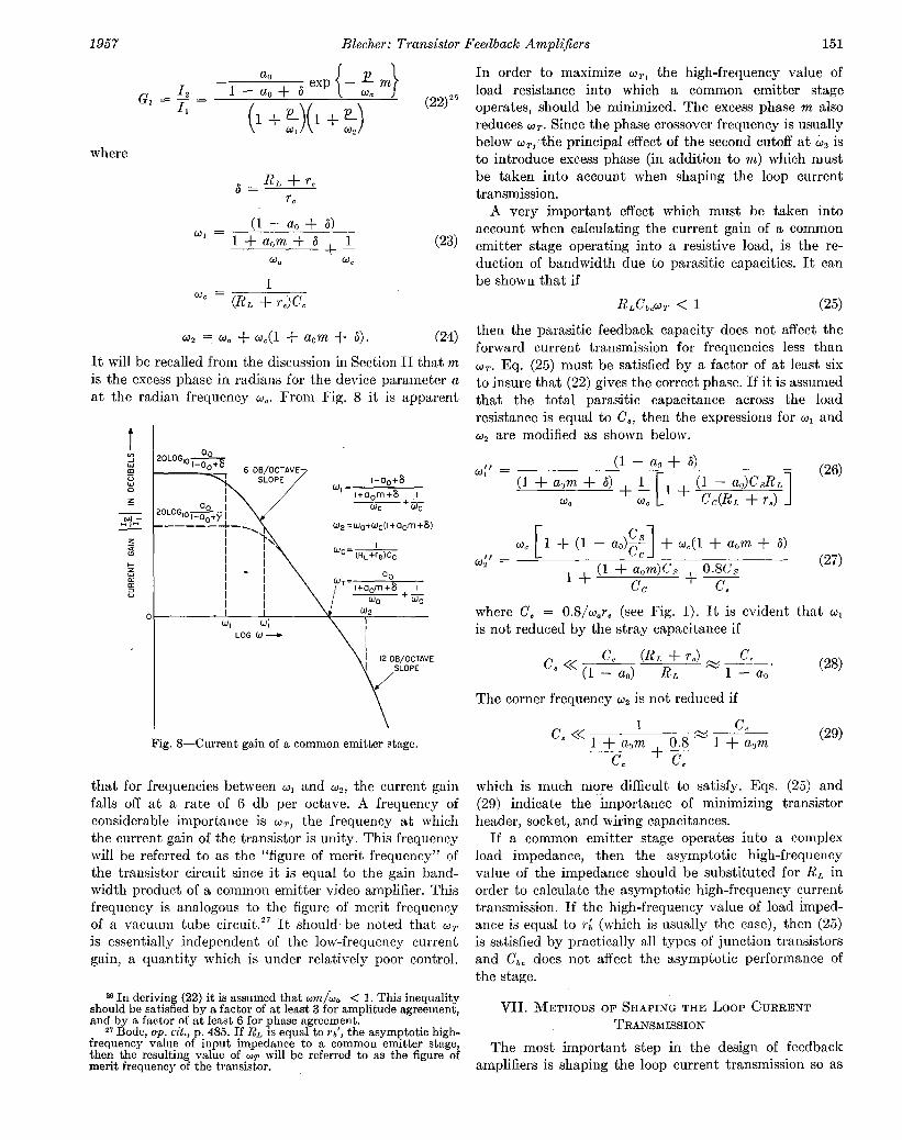
It will be recalled from the discussion in Section II that m is the excess phase in radians for the device parameter a at the radian frequency w,. From Fig. 8 it is apparent
LOG W-
Fig. S-Current gain of a common emitter stage.
that for frequencies between w1 and wZ, the current gain falls off at a rate of 6 db per octave. A frequency of considerable importance is wT, the frequency at which the current gain of the transistor is unity. This frequency will be referred to as the “figure of merit frequency” of the transistor circuit since it is equal to the gain band- width product of a common emitter video amplifier. This frequency is analogous to the figure of merit frequency of a vacuum tube circuit.” It should be noted that wT is essentially independent of the low-frequency current gain, a quantity which is under relatively poor control.
20 In deriving (22) it is assumed that wm/& < 1. This inequality should be satisfied by a factor of at least 3 for amplitude agreement, and by a factor of at least 6 for phase agreement.
,27 Bode, op. cit., p. 48.5. If RL is equal to rb’, the asymptotic high- frequency value of input impedance to a common emitter stage, then the resulting value of WT will be referred to as the figure of merit frequency of the transistor.
In order to maximize wT, the high-frequency value of load resistance into which a common emitter stage operates, should be minimized. The excess phase m also reduces wT. Since the phase crossover frequency is usually below w.,:the principal effect of the second cutoff at WZ is to introduce excess phase (in addition to m) which must be taken into account when shaping the loop current transmission.
A very important effect which must be taken into account when calculating the current gain of a common emitter stage operating into a resistive load, is the re- duction of bandwidth due to parasitic capacities. It can be shown that if
RLC~AJJT < 1 (25)
then the parasitic feedback capacity does not affect the forward current transmission for frequencies less than wT. Eq. (25) must be satisfied by a factor of at least six to insure that (22) gives the correct phase. If it is assumed that the total parasitic capacitance across the load resistance is equal to C,, then the expressions for w1 and o2 are modified as shown below.
I! = (1 - a0 + 6) Wl
(1 + a,m + 6) l + (1 - a,K’sRr, (W
W, Cc@, + ye) 1 + w,(l + aom + 6)
(27)
where C, = O.S/w,r, (see Fig. 1). It is evident that w1 is not reduced by the stray capacitance if
c8 K (1 “‘a,,) (RL + r,) CC .
R, *l-oa, (28)
The corner frequency o2 is not reduced if
c. << 1 cc
1 + aom 0.8 k5 1 + aom (29
c, +c,
which is much more difficult to satisfy. Eqs. (25) and (29) indicate the importance of minimizing transistor header, socket, and wiring capacitances.
If a common emitter stage operates into a complex load impedance, then the asymptotic high-frequency value of the impedance should be substituted for R, in order to calculate the asymptotic high-frequency current transmission. If the high-frequency value of load imped- ance is equal to rL (which is usually the case), then (25) is satisfied by practically all types of junction transistors and Cbc does not affect the asymptotic performance of the stage.
VII. METHODS OF SHAPING THE LOOP CURRENT TRANSMISSION
The most important step in the design of feedback amplifiers is shaping the loop current transmission so as
152 IRE TRANSACTIONS ON CIRCUIT THEORY September
to provide the maximum amount of feedback in the useful band together with adequate margins against instability. This subject has been completely discussed for ,single loop feedback amplifiers by Bode, including the effect of excess phase.” This section is devoted to a brief discussion of some useful methods for shaping the loop current transmission. These methods are illustrated in Section VIII by the design of a carrier-frequency feedback amplifier.
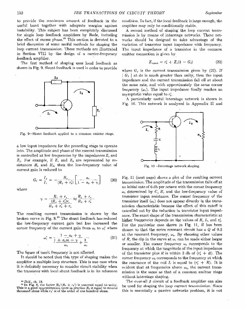
The first method of shaping uses local feedback as shown in Fig. 9. Shunt feedback is used in order to provide
Fig. S-Shunt feedback applied to a common emitter stage.
a low input impedance,for the preceding stage to operate into. The amplitude and phase of the current transmission is controlled at low frequencies by the impedances 2, and 2,. For example, if 2, and 2, are represented by re- sistances R, and R,, then the low-frequency value of current gain is reduced to
R Gr = 2 = -(RZ-?i L _ [ a, _ aI + Y 1 (30)
where
The resulting current transmission is shown by the broken curve in Fig. 8.” The shunt feedback has reduced the low-frequency current gain but has increased the corner frequency of the current gain from w1 to w{ where
I- l-a,+7 w1 - 1 + a,m + y c 1’ (31)
.Wa I WC
The figure of merit frequency is not affected. It should be noted that this type of shaping makes the
amplifier a multiple loop structure. This is one case when it is definitely necessary to consider circuit stability when the transistor with local shunt feedback is in its reference
2R Ibid., ch. 18. 29 In Fig. 8, the factor Rd/(RP -+ rb’) is assumed equal to unity.
This is a good approximation since in practice RZ is equal to several thousand ohms while rb’ is of the order of one hundred ohms.
condition. In fact, if the local feedback is large enough, the amplifier may only be conditionally stable.
A second method of shaping the loop current trans- mission is by means of interstage networks. These net- works should be designed to take advantage of the variation of transistor input impedance with frequency. The input impedance of a transistor in the common emitter connection is given by
Zinput = r,’ + Z,(l - Gr) (32)
where G, is the current transmission given by (22). If 1 G, 1 at dc is much greater than unity, then the input impedance and the current transmission fall off at about the same rate, and with approximately the same corner frequency (wl). The input impedance finally reaches an asymptotic value equal to r;.
A particularly useful interstage network is shown in Fig. 10. This network is analyzed in Appendix II and
Fig. lo-Inter&age network shaping.
Fig. 11 (next page) shows a plot of the resulting current transmission. The amplitude of the transmission falls off at an initial rate of 6 db per octave with the corner frequency w3 determined by C, R, and the low-frequency value of transistor input resistance. The corner frequency of the transistor itself (wl) does not appear directly in the trans- mission characteristic because the effect of this cutoff is cancelled out by the reduction in transistor input imped- ance. The exact shape of the transmission characteristic at higher frequencies depends on the values of R, L, and r;. For the particular case shown in Fig. 11, R has been chosen so that the series resonant circuit has a & of 0.5 at the resonant frequency, w4. By choosing other values of R, the dip in the curve at w4 can be made either larger or smaller. The corner frequency wy, corresponds to the frequency at which the magnitude of the input impedance of the transistor plus R is within 3 db of (r; + R). The corner frequency ws corresponds to the frequency at which the reactance of the coil L is equal to (r; + R). It is evident that at frequencies above w6, the current trans- mission is the same’ as that of a common emitter stage without interstage shaping.
The over-all @ circuit of a feedback amplifier can also be used for shaping the loop current transmission: Since this is essentially a passive networks problem, it is not

Blecher: Transistor Feedback AmpliJiers 153
2OLOG,c
-z
i w:
LOGW-
1 -aa,,+6 w’ = 1 + aom + 6
@a +;
1 w3 =
d-l-R+ r.0 + s>
l-aa,+ 1 c
-- w4- l& r,(l + 6)
rL+R+l-a
0
+a 1 wg = 6 + R 6 -I- R W6 = __ L
Fig. 11-Current gain with interstage network shaping.
discussed. A typical /? circuit design is illustrated in Section VIII.
VIII. AN ILLUSTRATIVE AMPLIFIER DESIGN
The design techniques discussed in this paper will now be demonstrated by the design of a carrier-frequency feedback amplifier. The amplifier must satisfy the follom- ing requirements:
1) External voltage gain of 36 db, flat within 0.1 db between 2000 cps and 1 me.
2) Input and output impedances must match a 600-ohm cable within 5 per cent, over the useful band without matching transformers.
3) Output power of 0.1 mw with total distortion at least 60 db below the fundamental.
4) Noise figure less than 9 db. In order to meet the above requirements on gain and distortion, it was decided that the amplifier required about 34 db of negative feedback. The transistors used were the type L5108 surface barrier transistors, which have the following average device parameters:
f. = 80 me
cc = 3 P&f
rl = 200 ohms
a 0 = 0.97
Cb6 + cc, = 3 wf.
Their maximum permissible power dissipation is 10 mw. Fig. 12 shows the complete circuit diagram of the amplifier.
22,ooon
I, II II
4 UUF 3.5 UUF 62 RK 4
5ooon +t ‘I
I5.000n.
E3
-1 d
145on
:6OOfi
Fig. 12-Circuit diagram of one-mc carrier-frequency feedback amplifier.

154 IRE TRANSACTIONS ON CIRCUIT THEORY
The over-all shunt feedback reduces the impedance at the base of the input stage and the collectoh of the output stage to less than 30 ohms (refer to Section IV). The input and output impedance requirements are satisfied by padding the amplifier with two 580-ohm resistors. This degrades the noise figure by approximately 3 db and reduces the output power by 3 db. The first two stages are biased at 1 ma of collector current and 2.5 volts collector voltage, while the third stage is biased at 2 ma collector current and 2 volts collector voltage.
September
It can be shown that the voltage gain of the amplifier is given by
E RK AP -A=-- El R.,W [I 7 API
where W is the ratio E,/E,“’ and Ap is the loop current transmission. For the circuit values shown in Fig. 12, the external voltage gain is exactly 36 db.
The first step in shaping the high-frequency end of Ap is to calculate the current transmission of each stage (refer to (22) for the first and second stages, and (30) and (31) for the third stage3’). In calculating w, for the first and second stages, RL should be assumed equal to r;, the high-frequency value of load resistance. Even though this gives too large a value for w,, it giyes the correct high- frequency asymptote which is required at this point in the design. When the effect of the over-all /3 network is taken into account,32 one obtains the so-called “un- shaped” loop transmission characteristic shown in Fig. 13. It has been found from experience that transistor feedback amplifiers require at least a IO-db gain margin and a 30” phase margin. Consequently, W. is determined as the frequency at which 1 A/3 I is equal to - 10 db. The width of the Bode step must be adjusted so that the phase angle introduced by the semi-infinite rising asymptote at wd compensates for the semi-infinite falling asymptote at W, plus excess phase. It will be assumed that the excess phase due to the device parameter a and the excess phase due to the cutoff at w2 (22) increase linearly with frequency. Consequently, for perfect phase compensation
(1 67) & = f%& + %f + 3wm -. (34)= TWd TfJJ. WZ WC2
Note that the rising asymptote at wd must have a slope of 10 db per octave (1.67 units) since the amplifier is to have a 30” phase margin. Measurements of excess phase on a number of L5108 transistors indicate that for a con- servative design, m should be 0.35 radians. The radian frequency wd is then calculated from (34). The Bode
30 It should be noted that W is determined essentially by passive elements since the base of the first stage is within 20 ohms of ground.
31 In this calculation, the tuned circuit in the local feedback path around the third stage should be neglected.
2.2 The fl circuit must be designed first to give the desired external voltage gain, plus rising asymptotes for the A@ characteristic at the lowest possible frequencies.
a3 The phase shift due to a semi-infinite slope of n units (a slope of one unit is 6 db per octave) starting at W,J for frequencies much less than wg, is given by 0 = (n) 2w/?rw0.
Fig. la-Determining ideal Bode cutoff.
Fig. 14--Asymptotic approximation to Bode cutoff.
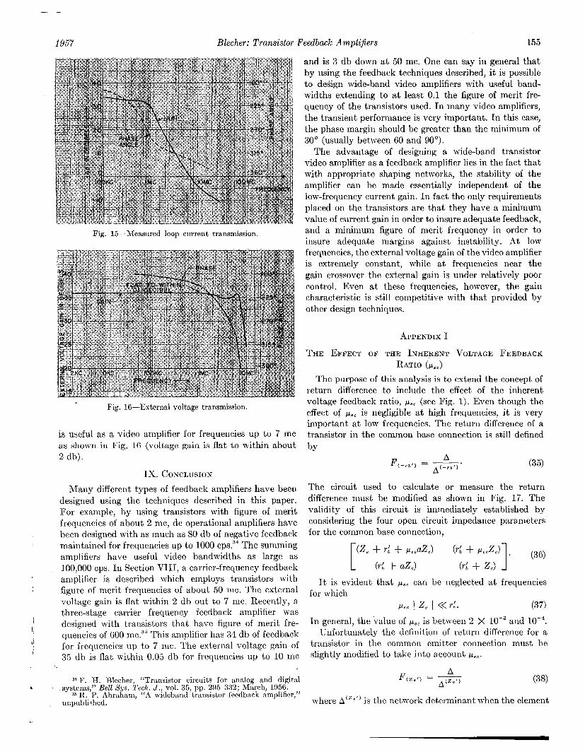
cutoff is completed as shown in Fig. 13. Fig. 14 shows the asymptotic approximation to the Bode cutoff. In this figure, ~33, w42, w52, and we2 refer to the corner frequencies introduced by the RLC shaping network in the base of the second stage (see Fig. 11). The frequency wl, refers to the cutoff of the first stage and w13 to the cutoff of the third stage (with local feedback). Finally, wBl, wj, refers to the gain doublet introduced by the 3.5~ppf condenser and wg2, wk, to the gain doublet introduced by the 4-PDF condenser, The fillet required at the top of the useful band (near wo) is approximated by the tuned circuit in the local feedback path around the third stage. Fig. 15 shows the resulting measured loop current transmission. The phase margin is 30” while the gain margin is about 10 db.
The feedback at low frequencies is shaped by means of two emitter bypass condensers. The 0.5~~crf condenser introduces a 6-db per octave cutoff at 2000 cps. The feedback continues to fall off at a rate less than 9 db per octave until 1 A@ 1 is much less than one.
Experimentally, the amplifier satisfies all of the re- quirements previously listed. In addition, the amplifier
Blecher: Trunsistor Feedback Amplifiers 155
Fig, 15-hleasured loop current transmission.
Fig. IG-External voltage transmission.
is useful as a video amplifier for frequencies up to 7 mc as shown in Fig. 16 (voltage gain is flat to within about 2 db).
IX. CONCLUSION
Many different types of feedback amplifiers have been designed using the techniques described in this paper. For example, by using transistors with figure of merit frequencies of about 2 mc, dc operational amplifiers have been designed with as much as 80 db of negative feedback maintained for frequencies up to 1000 CPS.~~ The summing amplifiers have useful video bandwidths as large as 100,000 cps. In Section VIII, a carrier-frequency feedback amplifier is described which employs transistors with figure of merit frequencies of about 50 mc. The external voltage gain is flat within 2 db out to 7 mc. Recently, a three-stage carrier frequency feedback amplifier was designed with transistors that have figure of merit fre- quencies of 600 mc.35 This amplifier has 34 db of feedback for frequencies up to 7 mc. The external voltage gain of 35 db is flat within 0.05 db for frequencies up to 10 mc
a4 F. I-1. Blccher, “Transistor cixllits for analog and digital systems,” Bell Sys. Tech. -T., vol. 35, pp. 295-332; March, 1956.
35 I?. P. Abraham, “-4 wideband transistor feedback amplifier,” unpublished.
and is 3 db down at 50 me. One can say in general that by using the feedback techniques described, it is possible to deiign wide-band video amplifiers with useful band- widths extending to at least 0.1 the figure of merit fre- quency of the transistors used. In many video amplifiers, the transient performance is very important. In this case, the phase margin should be greater than the minimum of 30” (usually between 60 and 90’).
The advantage of designing a wide-band transistor video amplifier as a feedback amplifier lies in the fact that with appropriate shaping networks, the stability of the amplifier can be made essentially independent of the low-frequency current gain. In fact the only requirements placed on the transistors are that they have a minimum value of current gain in order to insure adequate feedback, and a minimum figure of merit frequency in order to insure adequate margins against instability. At low frequencies, the external voltage gain of the video amplifier is extremely constant, while at frequencies near the gain crossover the external gain is under relatively poor control. Even at these frequencies, however, the gain characteristic is still competitive with that provided by other design techniques.
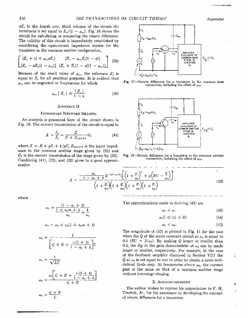
APPENDIX I
THE EFFECT OF THE INHERENT VOLTAGE FEEDBACK RATIO (CL,,)
The purpose of this analysis is to extend the concept of return difference to include the effect of the inherent voltage feedback ratio, F.. (see Fig. 1). Even though the effect of c(.~ is negligible at high frequencies, it is very important at low frequencies. The return difference of a transistor in the common base connection is still defined by
F(+‘) = --A-. *C-m’) (35)
The circuit used to calculate or measure the return difference must be modified as shown in Fig. 17. The validity of this circuit is immediately established by considering the four open circuit impedance parameters for the common base connection,
It is evident that pL,, can be neglected at frequencies for which
kc I Z, I <Cd. (37)
In general! the value of pL,, is between 2 X 10m3 and 10e4. Unfortunately the definition of return difference for a
transistor in the common emitter connection must be slightly modified to take into account wsC.
F A
(Zc’) = - A (20’) (38)
where A’““’ is the network determinant when the element
156 IRE TRANSACTIONS ON CIRCUIT THEORY September
aZ, in the fourth row, third column of the circuit de- tern&ant is set equal to Z,/(l - CL,,). Fig. 18 shows the I
circuit for calculating or measuring the return difference. The validity of this circuit is immediately established by , considering the open-circuit impedance matrix for the transistor in the common emitter configuration,
AMPLIFIER
L
EXCLUSIVE OF
(Z, + ri + k-aZ,> Fe - P~,.W - a>1 1 COMMON BASE STAGE IN % y ‘-Ii OUESTION
[Z, - a-%(1 - dl [Z, + -W - a>(1 - dl .N
Because of the small value of P.=, the reference Z[ is equal to Z, for all practical purposes. It is evident that pat can be neglected at frequencies for which Fig. 17-Return difference for a transistor in the common base
connection, including the effect of pee.
APPENDIX II
INTERSTAGENETWORKSHAPING
An analysis is presented here of the circuit shown in Fig. 10. The current transmission of the circuit is equal to AMPLIFIER
EXCLUSIVE OF COMMON EMITTER
STAGE IN OUESTION
N
where Z = R + pL + l/pC, Z,,,, is the input imped- ance to the common emitter stage given by (32) and G, is the current transmission of the stage given by (22). Fig. S-Return difference for a transistor in the common emitter Combining (41), (22), and (32) gives to a good approxi- connection, including the effect of pcC.
mation
A= - 1 - :; + 6 [e- (-)m] [ (1 + k)’ + p(RC - :)]
(1+9(1 +E)k +s +:) (42)
where
(1 - a, + 8) WI = 1 + a,m + 6
(Ja +;
w2 = 0, + 41 + am + 8
1 ws =
[
rdl + 6) r:+R+,-a,+6 1 c
ml rbl -k-B + re(l + 6) wg = l--C&+6 1 - 6 -I- R
rb’ + R W6Z------. L
The approximations made in deriving (42) are
w3 < WI
w,L << (d + R)
05 < (Jo.
(43)
(44)
(45)
The magnitude of (42) is plotted in Fig. 11 for the case when the Q of the series resonant circuit at wq is equal to 0.5 (RC = 2/w,). By making Q larger or smaller than 0.5, the dip in the gain characteristic at w& can be made larger or smaller, respectively. For example, in the case of the feedback amplifier discussed in Section VIII the Q at w4 is set equal to one in order to obtain a more mell- defined Bode step. At frequencies above wg, the current gain is the same as that of a common emitter stage without interstage shaping.
~.ACKNOWLEDGMENT‘ h The author wishes to express his appreciation to F. H.
Tendick, Jr., for his assistance in developing the concept of return difference for a transistor.