design and implementation of fpga-based systolic array for lz data compression
DESCRIPTION
Design and Implementation of FPGA-based systolic array for LZ Data Compression. By Mohamed Ahmed Abd El Ghany Ahmed. 2006. Overview. Introduction to Data Compression Data Compression Methods Systolic Array Operation in LZ Proposed design (Design-P) FPGA Implementation - PowerPoint PPT PresentationTRANSCRIPT
Design and Implementation of FPGA-based systolic array for
LZ Data Compression
ByMohamed Ahmed Abd El Ghany Ahmed
2006
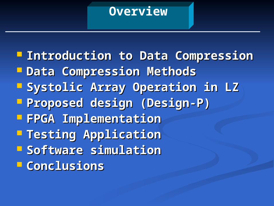
Overview
Introduction to Data CompressionIntroduction to Data Compression Data Compression Methods Data Compression Methods Systolic Array Operation in LZ Systolic Array Operation in LZ Proposed design (Design-P) Proposed design (Design-P) FPGA Implementation FPGA Implementation Testing Application Testing Application Software simulation Software simulation Conclusions Conclusions
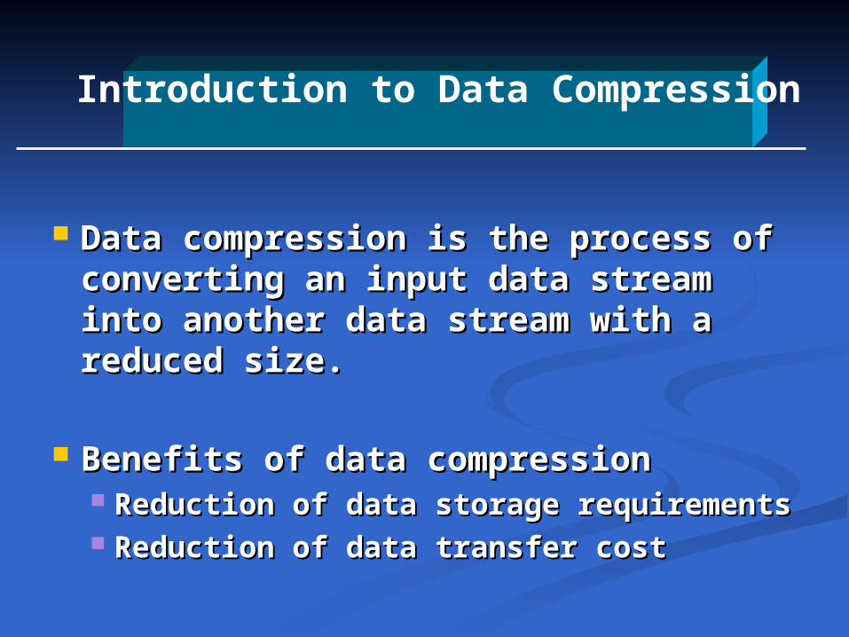
Data compression is the process of Data compression is the process of converting an input data stream into converting an input data stream into another data stream with a reduced another data stream with a reduced size.size.
Benefits of data compressionBenefits of data compression Reduction of data storage requirementsReduction of data storage requirements Reduction of data transfer costReduction of data transfer cost
Introduction to Data Compression
Data Compression Methods
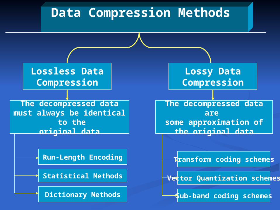
Lossy Data Compression
Lossless Data Compression
Transform coding schemes
Vector Quantization schemes
Sub-band coding schemes
Run-Length Encoding
Statistical Methods
Dictionary Methods
The decompressed data are
some approximation of the original data
The decompressed data must always be identical
to the original data
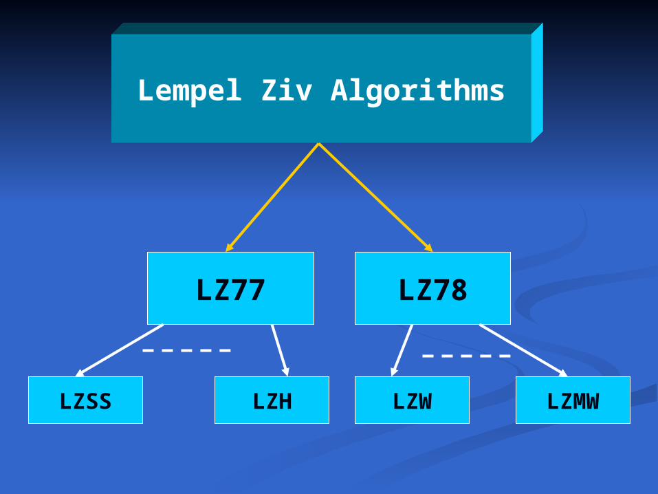
Lempel Ziv Algorithms
LZ78LZ77
LZSS LZH LZW LZMW
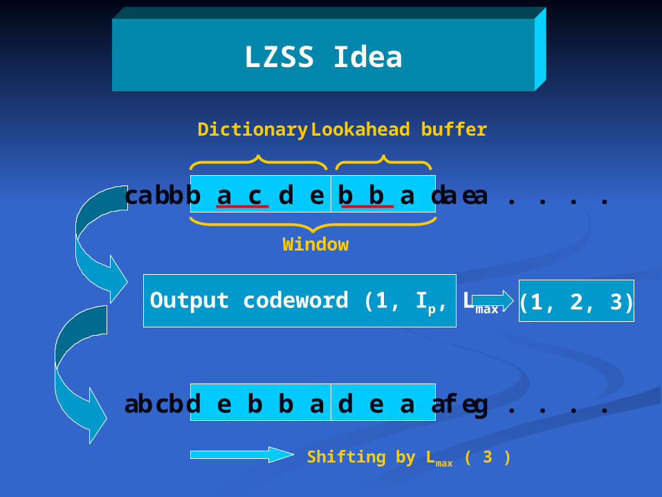
LZSS Idea
b b a d ec b b a c d e a a . . . . a b
Lookahead bufferDictionary
Window
Output codeword (1, Ip, Lmax) (1, 2, 3)
d e a a ea c d e b b a f g . . . . b b
Shifting by Lmax ( 3 )
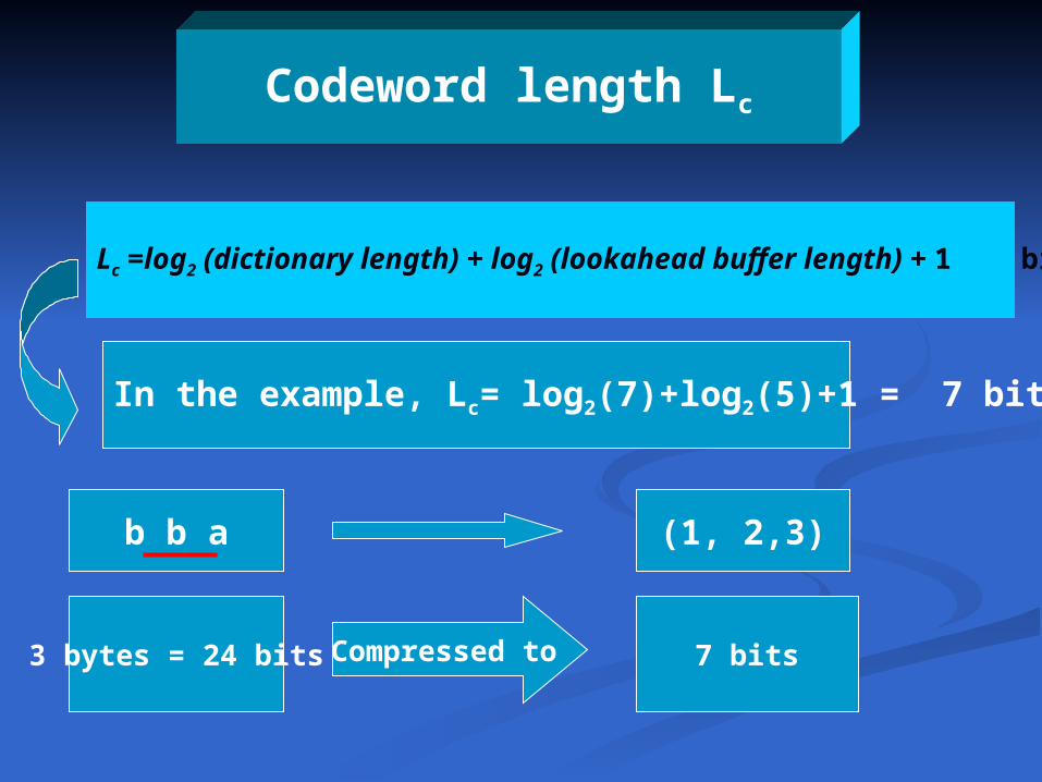
Codeword length Lc
In the example, Lc= log2(7)+log2(5)+1 = 7 bits
Lc =log2 (dictionary length) + log2 (lookahead buffer length) + 1 bits
b b a (1, 2,3)
3 bytes = 24 bits 7 bitsCompressed to
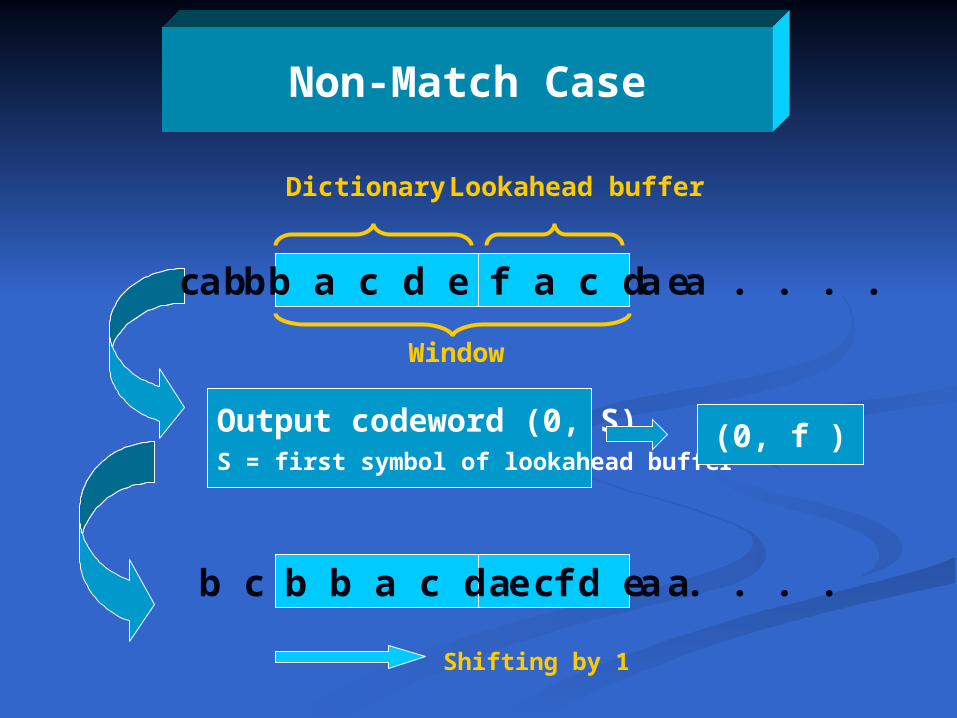
Non-Match Case
f a c d ec b b a c d e a a . . . . a b
Lookahead bufferDictionary
Window
Output codeword (0, S)S = first symbol of lookahead buffer
(0, f )
a c d e ab b a c d e f a . . . . b c
Shifting by 1
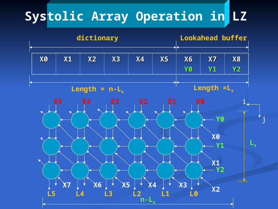
Systolic Array Operation in LZ
X0X0 X1X1 X2X2 X3X3 X4X4 X5X5 X6X6
Y0Y0X7X7
Y1Y1X8X8
Y2Y2
dictionary Lookahead buffer
Length = n-LsLength =Ls
E0
Y0
Y1
Y2
X0
X1
X2L0
E2
X4L2
X5
E3
L3
E5
X7L5
E1
L1X3X6
E4
L4
Ls
i
j
n-Ls
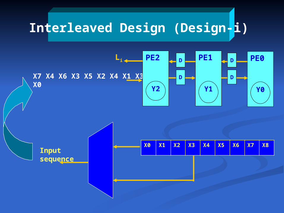
Interleaved Design (Design-i)
Li
X7 X4 X6 X3 X5 X2 X4 X1 X3 X0
PE2 PE1 PE0
DD
Y2 Y1 Y0
DD
Input sequenceX0 X1 X2 X3 X4 X5 X6 X7 X8
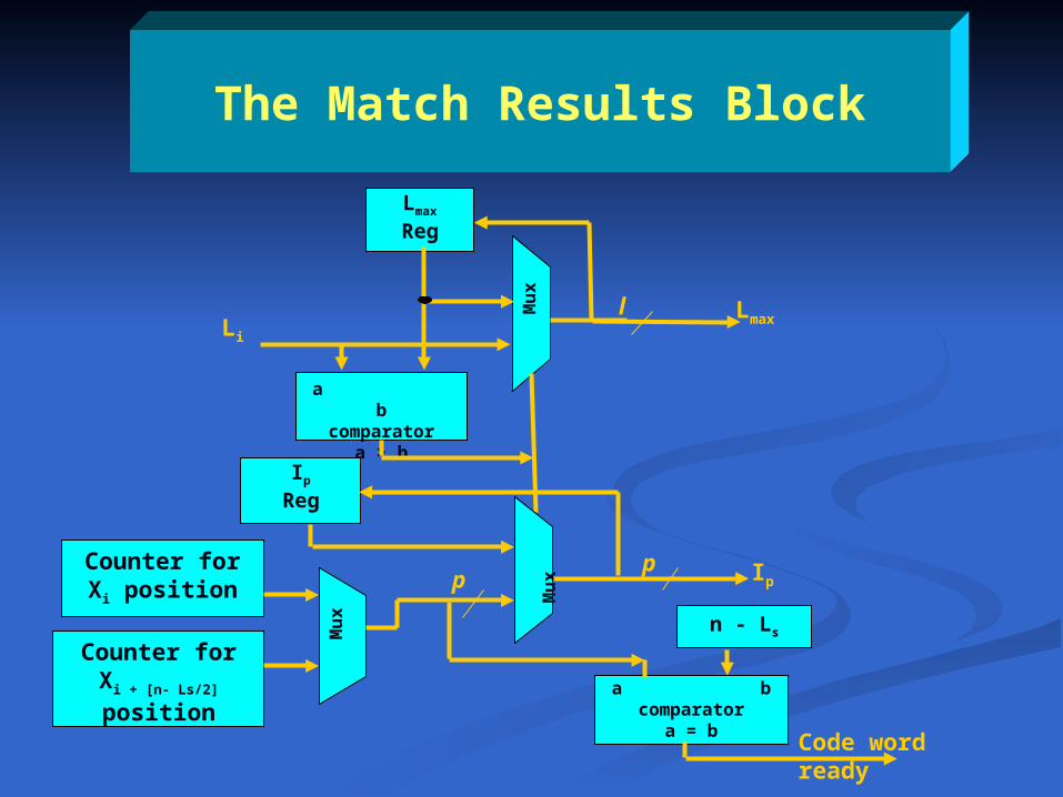
The Match Results Block
Code word ready
l
pp Ip
LmaxLi
Lmax
Reg
a bcomparator
a > b
M
ux
Ip
Reg
Mu
x
a bcomparator
a = b
n - Ls
Counter for Xi position
M
ux
Counter forXi + [n- Ls/2] position
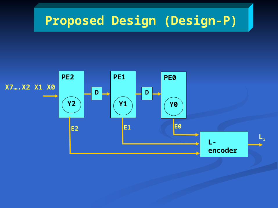
Proposed Design (Design-P)
E2 E1 E0
Li
X7….X2 X1 X0
PE2 PE1 PE0
DD
Y2 Y1 Y0
L-encoder
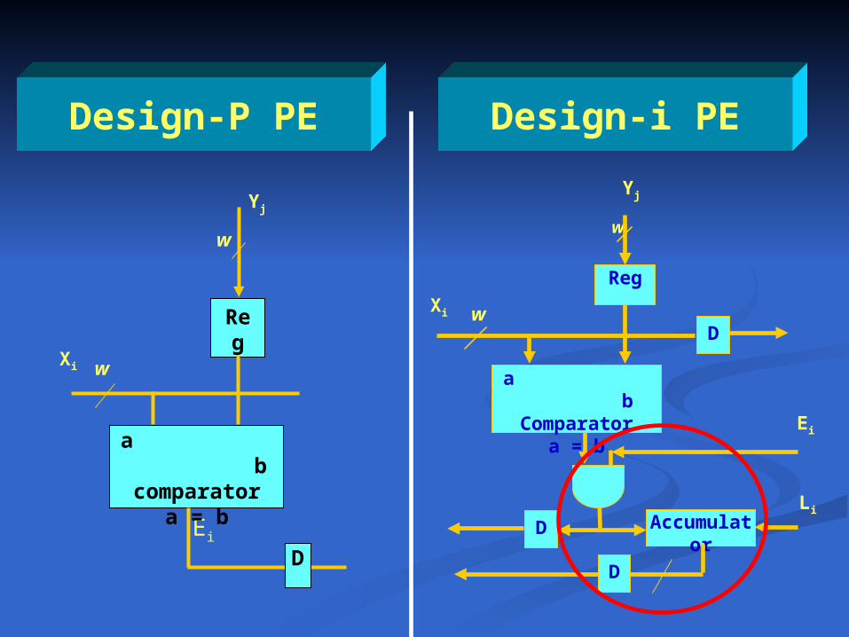
Design-P PE
Ei
Xi w
w
Reg
Yj
a bcomparator
a = b
D
Design-i PE
Li
Yj
Ei
Xi w
w
a bComparator
a = b
Reg
AccumulatorD
D
D
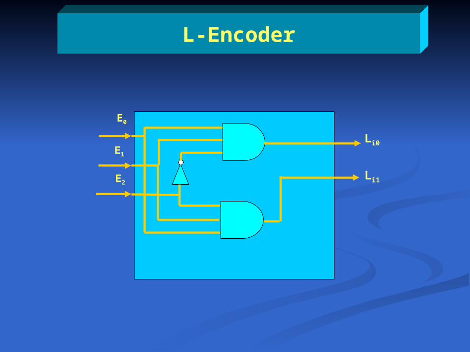
L-Encoder
Li1
Li0
E2
E1
E0
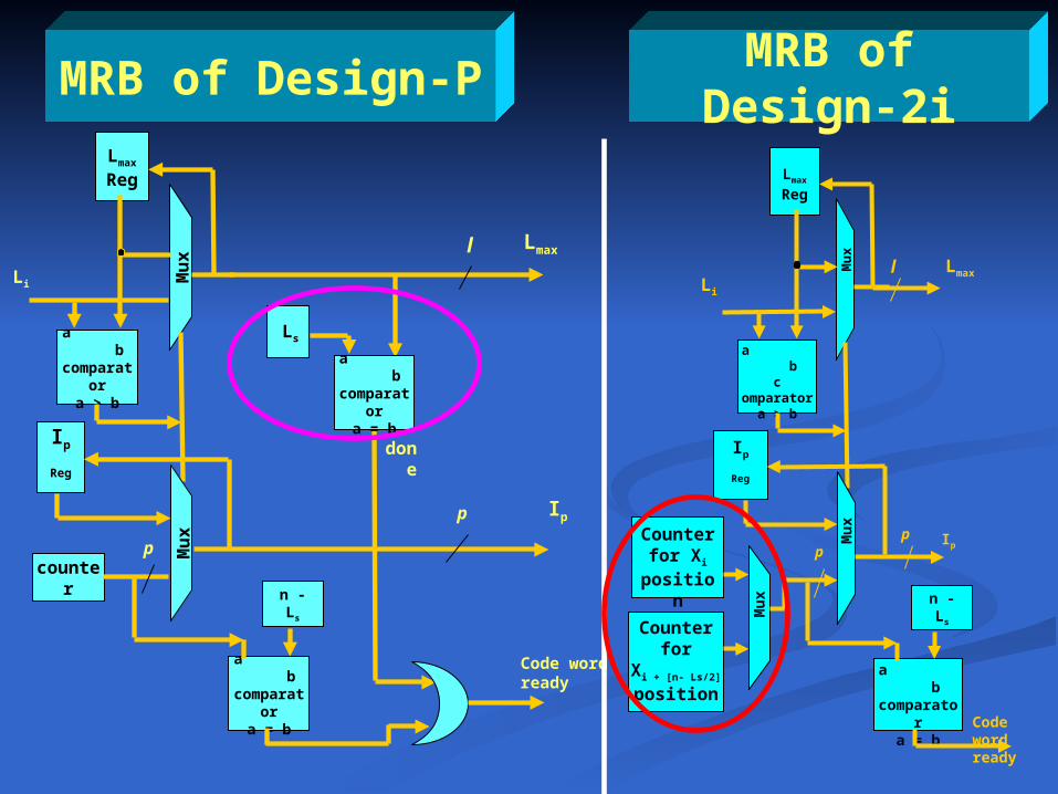
MRB of Design-P
l
p
p
Code word ready
done
Ip
Lmax
Li
Lmax
Reg
a bcomparator
a > b
Mu
x
Ip
Reg
Mu
x
counter
a bcomparator
a = b
n - Ls
Ls
a bcomparator
a = b
Code word ready
l
pp Ip
Lmax
Li
Lmax
Reg
a bc omparator
a > b
M
ux
Ip
Reg
M
ux
a bcomparator
a = b
n - Ls
Counter for Xi
position
M
ux
Counter forXi + [n- Ls/2] position
MRB of Design-2i
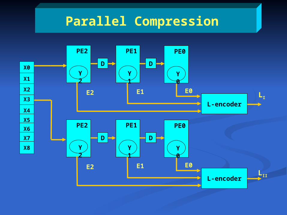
Parallel Compression
E2 E1 E0LI
PE2 PE1 PE0
DD
Y2
Y1
Y0
L-encoder
E2 E1 E0
PE2 PE1 PE0
DD
Y2
Y1
Y0
L-encoderLII
X0
X1
X3
X4
X5
X6
X7
X8
X2
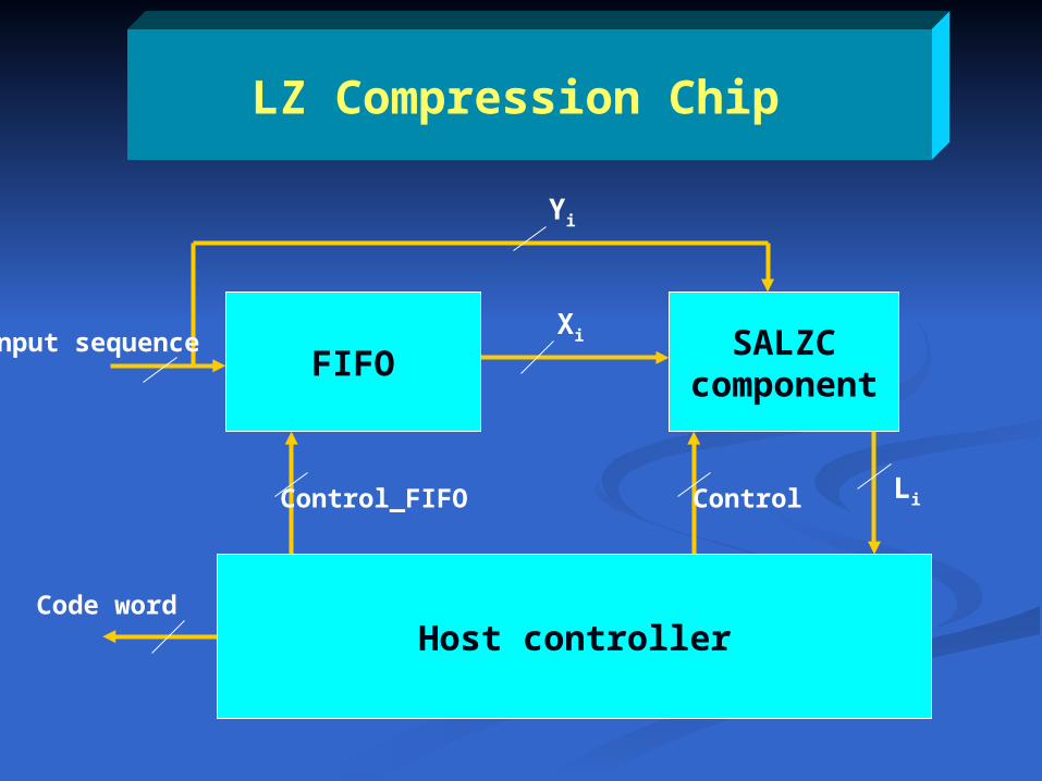
LZ Compression Chip
SALZC componen
tFIFO
Host controller
LiControl
Xi
Yi
Input sequence
Code word
Control_FIFO
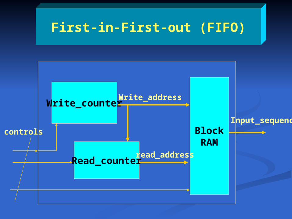
First-in-First-out (FIFO)
Block RAM
Write_counter
Read_counter
Write_address
read_address
Input_sequencecontrols
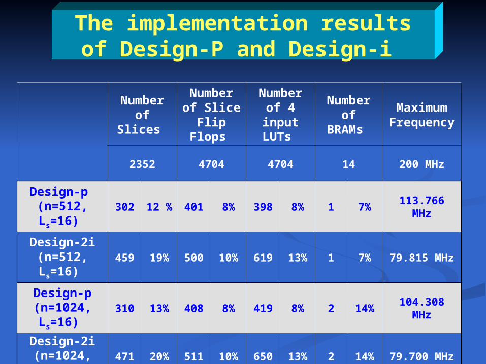
The implementation results of Design-P and Design-i
Number of Slices
Number of Slice
Flip Flops
Number of 4
input LUTs
Number of
BRAMs
Maximum Frequenc
y
2352 4704 4704 14 200 MHz
Design-p (n=512, Ls=16)
302 12 % 401 8% 398 8% 1 7% 113.766 MHz
Design-2i (n=512, Ls=16)
459 19% 500 10% 619 13% 1 7% 79.815 MHz
Design-p (n=1024, Ls=16)
310 13% 408 8% 419 8% 2 14% 104.308 MHz
Design-2i (n=1024, Ls=16)
471 20% 511 10% 650 13% 2 14% 79.700 MHz
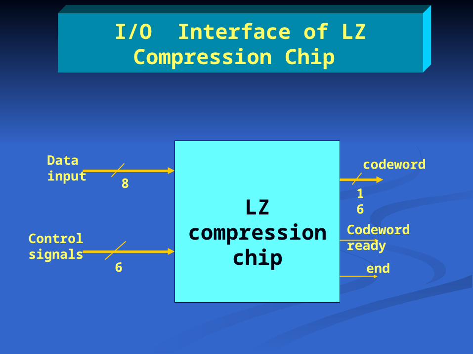
I/O Interface of LZ Compression Chip
end
Data input
LZ compression chipControl signals
codeword
Codeword ready
168
6
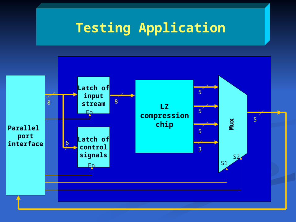
Latch of input
stream
Latch of control signals
8 8
6
En
En
5
5
5
3
Mu
x 5
LZ compressionchip
S2S1
Parallel port interface
8
Testing Application
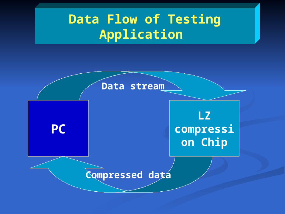
Data Flow of Testing Application
PC
Data stream
LZ compression Chip
Compressed data
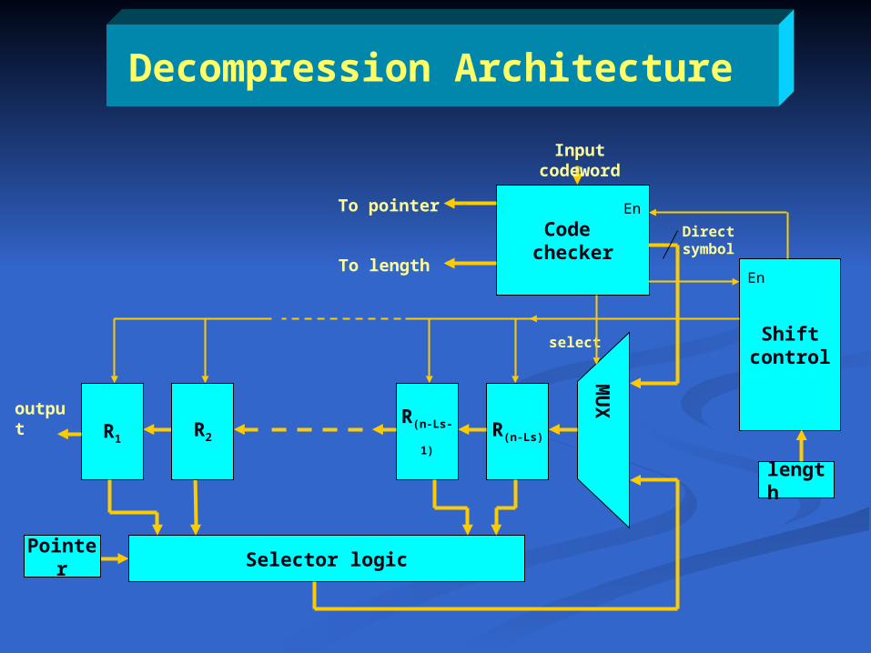
Decompression Architecture
Direct symbol
output
To pointer
To length
select
Code checker
Shift control
length
MU
X
R(n-Ls)R(n-Ls-1)R1
Selector logicPointer
En
En
Input codeword
R2
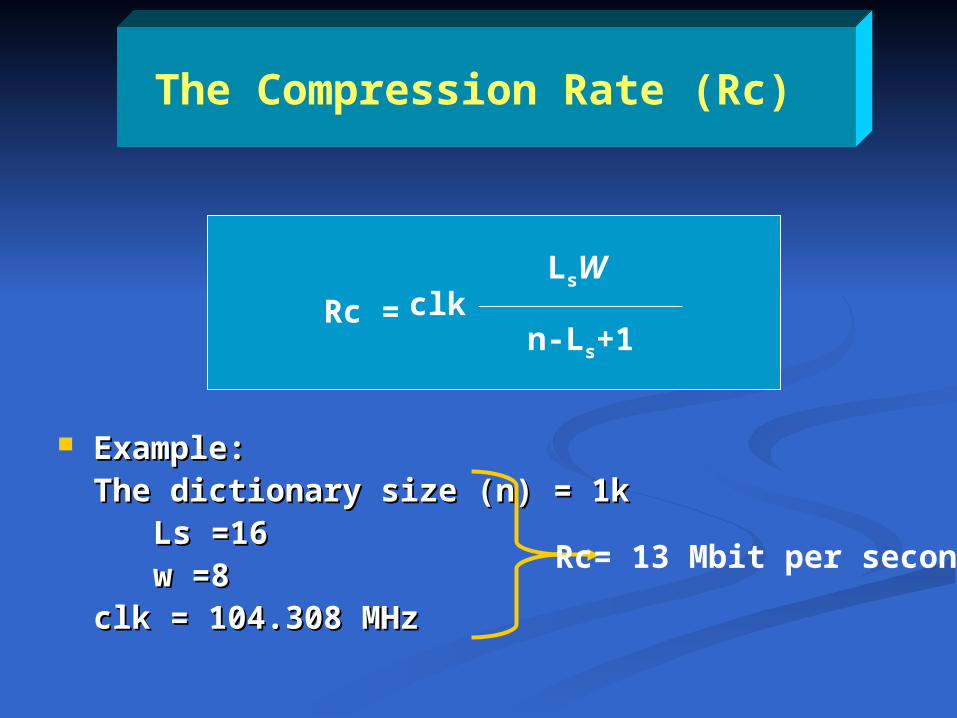
The Compression Rate (Rc)
LsW
n-Ls+1clkRc =
Example:Example:The dictionary size (n) = 1k The dictionary size (n) = 1k
Ls =16 Ls =16 w =8 w =8
clk = 104.308 MHz clk = 104.308 MHz
Rc= 13 Mbit per second
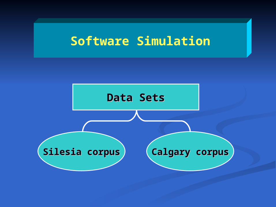
Software Simulation
Data SetsData Sets
Calgary corpusCalgary corpusSilesia corpusSilesia corpus
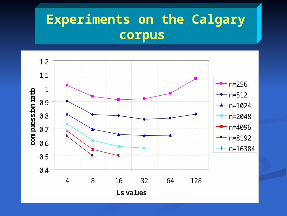
Experiments on the Calgary corpus
0.4
0.5
0.6
0.7
0.8
0.9
1
1.1
1.2
4 8 16 32 64 128
Ls values
com
pre
ssio
n r
atio
n=256
n=512
n=1024
n=2048
n=4096
n=8192
n=16384
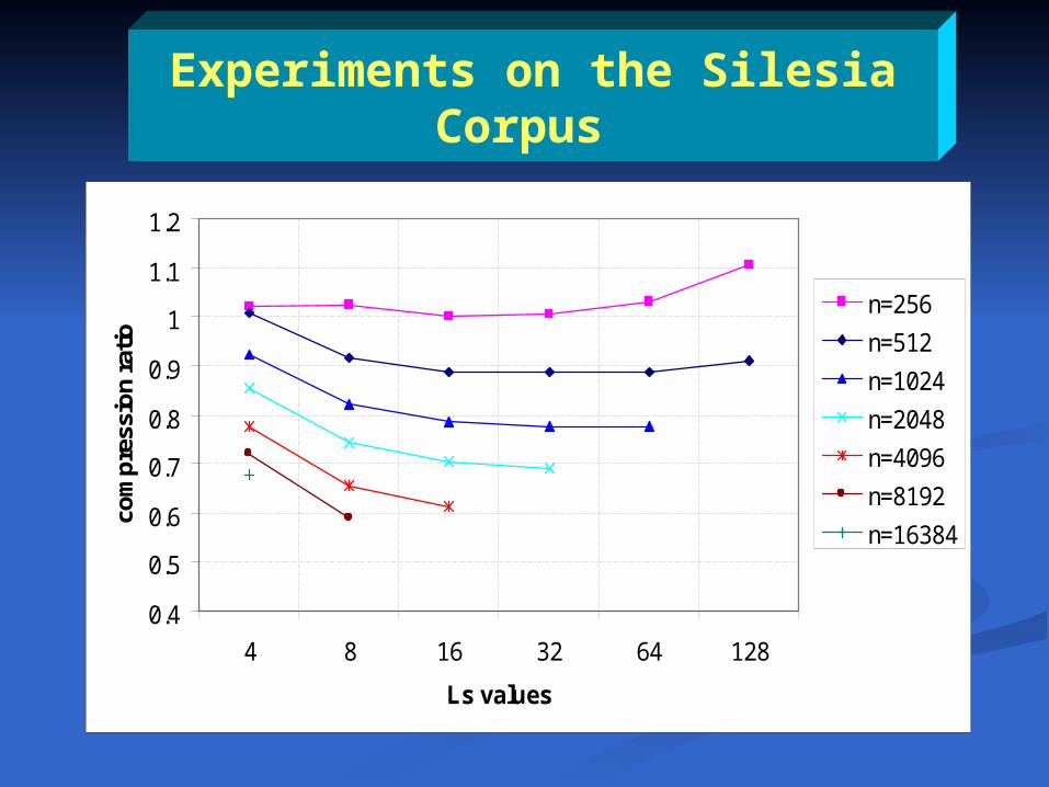
Experiments on the Silesia
Corpus
0.4
0.5
0.6
0.7
0.8
0.9
1
1.1
1.2
4 8 16 32 64 128
Ls values
com
pre
ssio
n r
atio
n=256
n=512
n=1024
n=2048
n=4096
n=8192
n=16384
Conclusions
The proposed implementation is area The proposed implementation is area and speed efficient. The compression and speed efficient. The compression rate is increased by more than rate is increased by more than 40%40% and the design area is decreased by and the design area is decreased by more than more than 30%.30%.
The prototype is executed using The prototype is executed using XILINX, Spartan II FPGA. XILINX, Spartan II FPGA.
The chip can be incorporated among The chip can be incorporated among real-time systems so that data can be real-time systems so that data can be compressed and decompressed on-compressed and decompressed on-the-fly. the-fly.
Future Work
Studying the effect of combining the Studying the effect of combining the proposed architecture for LZ data proposed architecture for LZ data compression and elliptic curve compression and elliptic curve cryptography in a single chip.cryptography in a single chip.
Study the fast string matching Study the fast string matching techniques are required to accelerate techniques are required to accelerate the compression process. the compression process.
By modifying the host controller and By modifying the host controller and including, e.g., dictionaries, our chip can including, e.g., dictionaries, our chip can be used for other string-matching based be used for other string-matching based LZ algorithms, such as LZ78 and LZW. LZ algorithms, such as LZ78 and LZW.

Thanks