design and characterization of an intensity modulated...
TRANSCRIPT

DESIGN AND CHARACTERIZATION OF AN INTENSITY MODULATED OPTICAL MEMS MICROPHONE
By
LEE HUNT
A THESIS PRESENTED TO THE GRADUATE SCHOOL OF THE UNIVERSITY OF FLORIDA IN PARTIAL FULFILLMENT
OF THE REQUIREMENTS FOR THE DEGREE OF MASTER OF ENGINEERING
UNIVERSITY OF FLORIDA
2003

Copywright 2003
By
Lee Hunt

iii
ACKNOWLEDGEMENTS
I wish to give my love and gratitude to my friends and family for all the love and
support I have received during the many years of my college career. I would never have
succeeded to the extent that I have without them. I especially appreciate the love and
support from my fiancée, Ms. Lisa Sewell, and for her ability to see through my
“preoccupied graduate student” exterior and find that which lies beneath.
I would also like to express my gratitude to my advisor, Dr. Toshikazu Nishida,
for recruiting me into IMG and giving me the educational tools and support needed to
complete a difficult project. Thanks also go to Dr. Mark Sheplak, Dr. Lou Cattafesta, and
Dr. Peter Zory for the excellent work they have done in teaching the classes that provided
the foundation for my research, and also for their guidance during the process. I also
wish to thank my friends and colleagues in the Interdisciplinary Microsystems Group
who have provided support. Special thanks go to Karthik Kadirval for his support in the
beginning of my work on the optical microphone project, and to Stephen Horowitz and
Robert Taylor for timely assistance when I needed it.
Financial support for this project is provided by DARPA (Grant #DAAD19-00-1-
0002) through the Center for Materials in Sensors and Actuators (MINSA) and is
monitored by Dr. Paul Holloway.
iv
TABLE OF CONTENTS
ACKNOWLEDGEMENTS............................................................................................... iii
ABSTRACT.........................................................................................................................x
CHAPTER
1 INTRODUCTION .......................................................................................................... 1
1.1. Optical Microphone Transduction Schemes............................................................ 1 1.1.1. Intensity Modulation......................................................................................... 2 1.1.2. Polarization Modulation.................................................................................... 5 1.1.3. Phase Modulation.............................................................................................. 6 1.1.4. Suitability of Transduction Techniques for MEMS Implementation ............... 9
1.2. Microphone Structure ............................................................................................ 12 1.2.1. Overview......................................................................................................... 12 1.2.2. MEMS Chip .................................................................................................... 14 1.2.3. Optical Fibers.................................................................................................. 15 1.2.4. Light Source.................................................................................................... 18 1.2.5. Detection Electronics ...................................................................................... 18
2 MICROPHONE SYSTEM PARTITIONING AND PERFORMANCE METRICS... 21
2.1. System Partitioning................................................................................................ 21 2.1.1. Acousto-Mechanical Stage ............................................................................. 21 2.1.2. Mechano-Optical Stage................................................................................... 21 2.1.3. Opto-Electrical Stage ...................................................................................... 22
2.2. System Performance Metrics ................................................................................. 22 2.2.1. System Sensitivity........................................................................................... 23 2.2.2. System Linearity ............................................................................................. 39 2.2.3. System Frequency Response........................................................................... 44 2.2.4. System Electronic Noise ................................................................................. 46 2.2.5. System Minimum Detectable Signal .............................................................. 51 2.2.6. Optical Reference Path Losses and System Performance Metrics ................. 55 2.2.7. Summary of Predicted System Performance .................................................. 57
3 DESIGN OF THE OPTICS FOR THE MEMS OPTICAL MICROPHONE ............. 59
3.1. Selection of the Optics........................................................................................... 59 3.1.1. Performance .................................................................................................... 59 3.1.2. System Connectivity ....................................................................................... 61 3.1.3. Ease of Handling and Manufacturability ........................................................ 61

v
3.1.4. Cost ................................................................................................................. 62 3.2. Selection of the Tubing.......................................................................................... 63 3.3. Alignment Issues.................................................................................................... 64
3.3.1. MEMS Chip Cavity Alignment issues............................................................ 64 3.3.2. Fiber Bundle Geometry Issues........................................................................ 67 3.3.3. Application of Alignment Theory to Fiber Bundle Selection......................... 68
4 FABRICATION OF THE OPTICAL MICROPHONE .............................................. 70
4.1. MEMS Exchange Process...................................................................................... 70 4.2. Packaging Process.................................................................................................. 71
5 EXPERIMENTAL SETUP AND RESULTS.............................................................. 79
5.1. Laser and Photodetector Characterization ............................................................. 80 5.1.1. Experimental Setup for Laser and Photodetector Characterization ................ 80 5.1.2. Results of Laser and Photodetector Characterization ..................................... 81
5.2. Static Calibration ................................................................................................... 81 5.2.1. Experimental setup for static calibration ........................................................ 81 5.2.2. Results of static calibration............................................................................. 84
5.3. Dynamic Calibration.............................................................................................. 87 5.3.1. Experimental setup for dynamic calibration ................................................... 87 5.3.2. Results of the dynamic calibration.................................................................. 90
6 CONCLUSIONS AND FUTURE WORK .................................................................. 99
6.1. Conclusions............................................................................................................ 99 6.2. Future Work......................................................................................................... 100
APPENDIX
A MEMS OPTICAL MICROPHONE DIAPHRAGM PROCESS FLOW.................. 102
B FIBER BUNDLE PROCESS FLOW........................................................................ 105
C MECHANICAL DRAWINGS.................................................................................. 117
D PHOTODETECTOR SPECIFICATIONS................................................................ 118
E SPECIFICATIONS FOR POPPER & SONS STEEL TUBING .............................. 119
LIST OF REFERENCES................................................................................................ 120
BIOGRAPHICAL SKETCH ..........................................................................................124

vi
LIST OF TABLES
1-1 – Summary of Intensity-Modulated Optical Microphone Designs ............................ 10
1-2 – Summary of Phase Modulated Optical Microphone Designs ................................. 11
2-1 – Acousto-Mechanical Lumped Element Parameters ................................................ 45
2-2 – Summary of Configuration Settings for Theoretical Performance Metrics ............ 57
2-3 – Summary of Theoretical System Performance Metrics........................................... 58
3-1 – Error Analysis of Different Fiber Bundle Configurations....................................... 69
4-1 – Wafers Used for Optical Microphone Fabrication .................................................. 70
5-1 – Experimental HP8168B Noise................................................................................. 81
5-2 – Comparison between Theoretical and Experimental Static Calibration.................. 86
5-3 – Experimental Results of Unreferenced Output Microphone Dynamic Calibration 98
5-4 – Experimental Results of Referenced Output Microphone Dynamic Calibration .... 98
vii
LIST OF FIGURES
1-1 – Optical Microphone Classification Based on Transduction Mechanism [2]............. 2
1-2 – Radiated Wave Intensity-modulating Microphone Types......................................... 3
1-3 – Evanescent Wave Intensity-modulating Microphone Types..................................... 4
1-4 – Polarization Modulating Microphone Types. ............................................................ 6
1-5 – Grating-Type Phase Modulating Microphone Types. ............................................... 7
1-6 – Interferometric Phase Modulating Microphone Types.............................................. 8
1-7 – Block Diagram of the Optical Microphone. ............................................................ 13
1-8 – Cross Section of the Fiber Bundle in the MEMS Chip. .......................................... 14
1-9 – Cross Section of the MEMS Chip. .......................................................................... 15
1-10 – End View of the Optical Fiber Bundle. ................................................................. 16
1-11 – Optical Fibers in Steel Tubing............................................................................... 16
1-12 – Optical Fiber Bundle Drawing. ............................................................................. 17
2-1 – Side View of Deflecting Plate or Membrane........................................................... 24
2-2 – Method of Images (View from Side of Fiber Bundle). ........................................... 27
2-3 – Ring Approximation Diagram. ................................................................................ 30
2-4 – Theoretical Power Coupled with Ideal Fiber Configuration. .................................. 32
2-5 – Theoretical Sensitivity with Ideal Fiber Configuration........................................... 32
2-6 – Block Diagram of the Unreferenced Output Configuration. ................................... 34
2-7 – Equivalent Circuit for the PDA400 Photodetector. ................................................. 35

viii
2-8 – Block Diagram of the Referenced Output Configuration........................................ 36
2-9 – Comparison of Unreferenced and Referenced Output Sensitivities........................ 39
2-10 – Linearity of Mechano-Optical Stage. .................................................................... 41
2-11 – Plot of Acousto-Mechanical Sensitivity as a Function of Radial Position............ 42
2-12 – Noise Contributions for the Photodetector Output. ............................................... 46
2-13 – Noise Contributions for the Microphone Output................................................... 48
2-14 – Illustration of the Physics Behind the MO MDS................................................... 53
3-1 – Bundle Position Error Illustration. .......................................................................... 65
3-2 – Angular Misalignment Error Illustration................................................................. 66
3-3 – Radial Position Error Illustration............................................................................. 67
4-1 – Abeysinghe et al. Packaging Technique.................................................................. 71
4-2 – Beggans et al. Packaging Technique. ...................................................................... 73
4-3 – Kadirval Packaging Technique................................................................................ 74
4-4 – Proposed Package for the Optical Microphone. ...................................................... 76
4-5 – Proposed Optical Microphone Array Package. ....................................................... 77
5-1 – Experimental Setup for Laser Characterization....................................................... 80
5-2 – Block Diagram of Static Calibration. ...................................................................... 84
5-3 – Experimental Power Coupled vs. Equilibrium Gap. ............................................... 85
5-4 – Experimental Maximum Power Coupled Regression Line Slope. .......................... 86
5-5 – Unreferenced Output Optical Microphone Configuration....................................... 88
5-6 – Referenced Output Optical Microphone Configuration. ......................................... 89
5-7 – Linearity, Unreferenced Output Configuration. ...................................................... 91
5-8 – Linearity, Referenced Microphone Configuration. ................................................. 92

ix
5-9 – Magnitude Response, Unreferenced Microphone Configuration............................ 93
5-10 – Magnitude Response, Referenced Microphone Configuration. ............................ 94
5-11 – Phase Response, Unreferenced Microphone Configuration.................................. 94
5-12 – Phase Response, Referenced Microphone Configuration. .................................... 95
5-13 – Electrical Noise Floor, Both Microphone Configurations..................................... 97

x
Abstract of Thesis Presented to the Graduate School of the University of Florida in Partial Fulfillment of the Requirements for the Degree of Master of Engineering
DESIGN AND CHARACTERIZATION OF AN INTENSITY
MODULATED OPTICAL MEMS MICROPHONE
By
Lee Hunt
August 2003
Chairman: Toshikazu Nishida Major Department: Electrical and Computer Engineering
This thesis presents the design and characterization of an intensity-modulated
optical lever microphone. Microphone noise models from previous works are expanded
to include the light source and all electronics. Physical phenomena responsible for
limiting the microphone minimum detectable signal (MDS) are identified, and an
accurate model developed for use with an LED or laser light source. The sensitivity,
minimum detectable signal, and electronics noise are characterized by a scaling analysis
in which coupled equations for dependence on optical power, membrane radius,
photodetector gain, and optical losses in the reference path are presented. It was
discovered that, in this optical microphone geometry, the laser is the limiting factor in the
microphone MDS and electronics noise, and optical losses in the reference path can
improve microphone sensitivity, MDS, and noise floor for a referenced optical
microphone.

xi
An unreferenced electronic configuration and a referenced electronic
configuration were experimentally characterized using a laser as a light source. The
unreferenced optical microphone achieved a sensitivity of 0.032 mV / Pa, MDS of 65 dB
(re. 20 µPa), and dynamic range from 65 – 122 dB (re. 20 µPa). The referenced optical
microphone achieved a sensitivity of 1.77 mV / Pa, MDS of 47 dB (re. 20 µPa), and
dynamic range from 47 – 122 dB (re. 20 µPa). Both unreferenced and referenced
measurements were made at 1600 Hz with a bin width of 2 Hz.

1
CHAPTER 1 INTRODUCTION
Optical microphones vary widely in their construction, but all possess innate
resistance to electro-magnetic interference (EMI) and other harsh environments to which
other types of microphones are sensitive. This innate resistance is derived from the
separation of the optical sensing element from the electronics via optical fibers and
assumes the electronics are remotely located with respect to the test environment. In the
case where the electronics are not remotely located, the microphone package must isolate
the microphone electronics from the test environment.
MEMS technology provides a promising new implementation for optical
microphones. MEMS devices have the capability to be smaller than conventional
microphones, and MEMS microphone chips could be processed by the thousand on
wafers if the market can support this volume. Despite these advantages, Professor Steve
Senturia [1] notes that MEMS devices have a coupling between the package and the
device, thus requiring them to be designed concurrently, which makes a MEMS
microphone design inherently more complicated than a conventional (non-MEMS)
microphone.
1.1. Optical Microphone Transduction Schemes
In 1996, Nykolai Bilaniuk first introduced a classification scheme for optical
microphones that relied on the transduction mechanism as the primary sorting criterion
[2]. He also explained the methods of operation of multiple types of devices in each

2
category, with emphasis on the most promising technologies, and he also discussed
microphone system performance metrics.
Bilaniuk defined three properties of light that could be modulated: the intensity
(or irradiance), the phase, and the polarization [2]. Since electro-optical detectors
respond to light intensity, all modulation schemes must be reduced to an intensity
modulation at the electronics end of the system. The figure below adapted from [2]
shows a detailed classification scheme for optical microphones.
Figure 1-1 – Optical Microphone Classification Based on Transduction Mechanism [2].
1.1.1. Intensity Modulation
Bilaniuk [2] describes an intensity-modulated microphone as one which
selectively removes energy from the optical path. As shown in Figure 1-1, an intensity-
Optical Microphones
Intensity Modulating
Polarization Modulating
Phase Modulating
Radiated Wave
Evanescent Wave
Moving Grating
Lever
Cantilever
Macrobend
Microbend
Coupled Waveguide
Radiated Wave
Evanescent Wave
Grating Interferometric
Michelson Interferometer
Mach-Zehnder Interferometer
Fabry-Perot
Two-Mode Fiber
Dynamic Photorefractive
Grating
Input Coupling Grating

3
modulating optical microphone can be subdivided into two broad categories: radiated
wave and evanescent wave. All of the energy in radiated wave optical microphone leaves
a controlled optical path and partially recaptured or backscattered [2]. Figure 1-2
recreates Bilaniuk’s [2] illustration of the radiated wave transduction strategies.
Figure 1-2 – Radiated Wave Intensity-modulating Microphone Types.
The moving grating approach relies on the motion of a “light gate” to modulate
the light coupled between an input waveguide and an output waveguide. These types of
devices do not make use of diffraction or any structures on the order of the wavelength of
the light.
An intensity-modulated lever microphone utilizes one or more waveguides to
deliver light to a vibrating plate or membrane. Reflected light is collected by one or more
Moving Grating Cantilever
Lever Macrobend

4
waveguides and delivered to a photodetector. Lever microphones may also have
focusing optics to improve light collection.
In a cantilever microphone, the waveguide is discontinuous, and part is free to
vibrate in an acoustic field. This varies the alignment between the fixed segment and the
free segment of the waveguide, causing a modulation of the power coupled.
Macrobend-type intensity-modulating schemes use acoustic waves to deform a
fiber configuration, such as a coil. Optical fibers are chosen that do not completely
confine the light. The deformation modulates the losses in the length of fiber,
subsequently modulating the output power.
Alternatively, the evanescent-wave coupling methods “rely on …mode coupling
or on absorption from the evanescent field” [2]. Bilaniuk defines two classes of
evanescent wave intensity-modulating microphones: microbend and coupled waveguide.
Figure 1-3 recreates Bilaniuk’s [2] illustration of the evanescent wave intensity
modulation techniques.
Figure 1-3 – Evanescent Wave Intensity-modulating Microphone Types.
Microbend Coupled Waveguide

5
The microbend technique uses a microstructure to apply periodic deformations to
a waveguide. The acoustic field modulates the pressure exerted on the waveguide by
these deformations, which in turn causes leakage of power out of the waveguides.
The coupled waveguide technique can work in one of two different ways. In the
first way, the waveguides are fabricated on a membrane structure with a fixed separation
between the two. The membrane deflects in the presence of an acoustic field, and this
deflection changes the index of refraction in the two waveguides. The change in
refractive index modulates the power coupled between the waveguides. Alternately, the
waveguides are fabricated so that one is attached to a structure, while the other is free to
vibrate. An acoustic field will modulate the separation between the waveguides, which
modulates the power coupled between the two.
1.1.2. Polarization Modulation
The second major category of optical microphones as defined by Bilaniuk [2] is
polarization modulation. Polarization modulation type devices alter the polarization of
the light when in the presence of an acoustic field. Bilaniuk [2] subdivides polarization
modulation devices into two subcategories, but he notes that alternate schemes are
possible. Figure 1-4 adapted from [2] depicts the two subcategories.
In the first category, a layer of liquid crystals is subjected to acoustic field
induced shear stresses, which modulate the polarization of the light passing through. A
polarizer is located at the output of the device to isolate the desired polarization axis.
In the second category, “a moveable dielectric plate interacts with the evanescent
field of a waveguide excited with both TE and TM modes, causing a different change in

6
the refractive index of the two modes, according to Bilaniuk [2]”. A polarizer at the
output isolates the desired polarization axis.
Figure 1-4 – Polarization Modulating Microphone Types.
1.1.3. Phase Modulation
Phase modulated optical microphones are described by Bilaniuk [2] as a
mechanism that “changes either the physical length or the refractive index of an optical
test path and recombining the result with the signal from a reference path.” The reference
path is unaffected by the acoustic field, while the test path undergoes some form of
mechanical deformation. The two defined subgroups for this category of optical
microphones are grating type devices and interferometric devices.
A grating type device is one with a structure machined onto a waveguide with
features on the order of the wavelength of the light. The two different subcategories of
grating devices defined by Bilaniuk [2] are input coupling gratings and dynamic
refractive gratings. They are shown in the following figure, adapted from Bilaniuk [2].
Nematic Liquid Crystal Differential Index Shifter

7
Figure 1-5 – Grating-Type Phase Modulating Microphone Types.
The input coupling grating device has a grating fabricated on the waveguide.
Incident light at the proper angle, wavelength and with the proper grating spacing will be
coupled into the waveguide. The acoustic field modulates a nearby dielectric structure,
varying the index of refraction of the system and modulating the output.
The dynamic photorefractive grating uses a prism to split light onto two mirrors,
one of which is free to vibrate in an acoustic field. The light reflects off the mirrors to
pass through a grating, and the light from each mirror is captured by a photodetector.
The light from the stationary mirror is used as a reference signal, while the light from the
vibrating mirror is used as the modulated signal.
The second major category of phase modulating optical microphones is
interferometric-type phase-modulating microphones. They typically use one of the three
most familiar types of interferometers: Fabry-Perot, Michelson, or Mach-Zehnder.
Alternately, a two-mode fiber can be used to make a phase modulated microphone. The
figure below (adapted from [2]) depicts the four interferometric optical microphone
categories.
Input Coupling Grating Dynamic Photorefractive Grating

8
Figure 1-6 – Interferometric Phase Modulating Microphone Types.
The Fabry-Perot optical microphone uses an optical cavity formed between two
parallel surfaces. One of the surfaces is free to vibrate in an acoustic field, while the
other is fixed. Typically, the vibrating surface is a plate or membrane, and the fixed
reflecting surface is the face of the fiber, but additional optics may be used instead.
A Michelson optical microphone splits a free-space beam into two paths. The
reference path is reflected of a stationary reflector. The test path is reflected off of a
reflector that vibrates in an acoustic field. The beams recombine and interfere, and the
recombined signal is received by a photodetector.
In a Mach-Zehnder optical microphone, the light enters via a waveguide, which is
split into two paths. The reference path is held constant, but the test path is free to vibrate
Fabry-Perot Michelson
Mach-Zehnder Two-Mode Fiber

9
in an acoustic field. The light in the two paths is recombined and sent to a photodetector.
Interference effects will modulate the power seen by the detector.
The fourth type of interference optical microphone is a two-mode fiber
microphone. In this design, a section of two-mode optical fiber is spliced at the end of a
single mode fiber. The two-mode fiber is free to vibrate in an acoustic field. Acoustic
vibrations will modulate the index of refraction of each mode differently, and an
interference pattern will be generated at the junction between the two fibers.
1.1.4. Suitability of Transduction Techniques for MEMS Implementation
In general, the simplest type of microphone to analyze and build is an intensity-
modulated device. The simplest intensity-modulated device can be constructed with an
LED, multimode or single mode fibers, a membrane or other vibrating reflective surface,
and a photodetector.
Table 1-1 (see [3] – [8]) summarizes recent intensity-modulated optical
microphone designs. The results indicate a large variability in performance with the
implementation of the intensity-modulated microphone. While this observation may
seem obvious, it reinforces the importance of optimizing the system as a whole when
designing the microphone and not just an individual stage.
In general, for the intensity-modulated optical microphone, increasing the
diaphragm radius increases the sensitivity and decreases the minimum detectable signal
(MDS). Therefore, intensity-modulated microphone performance is decreased when the
diaphragm is constrained to have a diameter of less than a few hundred microns.

10
Table 1-1 – Summary of Intensity-Modulated Optical Microphone Designs
Author / Year Design Type Source and λo Sens Noise Freq Response
Linearity Range MDS
V. P. Klimashin 1979 [3]
Lever, -w- Support Optics, non MEMS
Incandescent Lamp 7.5 mV / Pa
20-22dB (re
20µPa)
0 - 20kHz -w- 5dB
fluctuations
- -
Hu and Cuomo 1992 [4]
Lever, -w- Mylar Membrane, Non
MEMS
LED, 2.4 mW
36.5 mV / Pa - 0-31.5
kHz - -
De Raula and Vinha
1992 [5]
Multiple Light Source non-MEMS
scheme
150 W Xenon Arc Lamp - 5.6 nW /
Hz0.5 - - -
Lukosz and Pliska
1992 [6]
Evanescent wave, microbend, 6x6 mm2
membrane
Laser, λ = 632.8 nm 0.31 Pa-1
49 dB (re
20µPa)
Up to 10kHz
49 dB - 95 dB -
Suhadolnik, et al.
1995 [7]
Lever, fiber bundle and deflecting
diaphragm, non-MEMS
- -
High due to
speckle pattern of laser
light
- MO Stage 1500 µm -
Kadirvel 2002 [8]
Lever, fiber bundle and deflecting
diaphragm
Laser, λ = 1550 nm
152 µV / Pa
110 dB (re
20µPa)
1 kHz – 6.4 kHz
110 dB – 135 dB
110 dB (re 20 µPa)
The choice of light source and photodetector also plays a large role in the
performance of an intensity-modulated OM. Both affect the device sensitivity and noise
floor. Sensitivity increases as coupled optical power increases, so high intensity light
sources provide higher sensitivities, provided that the photodetector does not saturate.
A disadvantage of all intensity-modulated OMs is the large DC component of the
received signal. The DC component does not contribute to the device sensitivity, but it
does contribute to photodetector saturation. This limits the product of the optical
received power and the detector trans-impedance gain. The maximum intensity of the
light source is limited by the linearity range and gain of the detector.
Table 1-2 (see [9] – [15]) summarizes recent phase modulated optical microphone
(PM) designs. Since no standard method of reporting the sensitivity of an optical
microphone has been agreed upon, it is difficult to compare the overall performance of

11
different PM designs. Theoretically, a PM device would be able to provide higher
performance than an intensity-modulated microphone in a MEMS implementation,
especially for membranes constrained to be smaller than a few hundred microns in
diameter. PM devices have a smaller DC component allowing for more flexibility in
selecting photodetector gain settings.
Table 1-2 – Summary of Phase Modulated Optical Microphone Designs
Author / Year Design Type Source and λo
Sens SNR Freq Response
Linearity Range Resolution
Rao et al. 1997 [9]
Bragg Grating –w- Fizeau Cavity
20mW LED @
λo=1550nm 12 pm / µε 50dB > 1kHz <
5000µε -
Furstenau et al. 1998 [10] Fabry-Perot Cavity
0.5mW (after pigtail)
LED @ λo=1300nm
Varies by 80dB over freq range w.r.t. B&K
4134
-
Tested over
100Hz to 15kHz
- -
Du et al. 1999 [11] Fiber Bragg Grating LED @
λo=1550nm 1.5 pm / µε - NA < 1200µε +/- 29µε
Graywall 1999 [12]
Surface-machined Fabry-Perot Cavity, theoretical analysis
LED @ λo=650nm 8.9 mV / Pa > 100 100Hz to
2kHz - -
Rao et al. 2000 [13]
Fiber Bragg Grating and Fizeau Cavity
20mW LED @
λo=1550nm ~ 540o / µm - - - -
Abeysinghe et al. 2001 [14]
Fabry-Perot Cavity machined on surface
of optical fiber
LED @ λo=850nm
0.11 mV / psi
(16 mV / MPa)
- NA 0 – 80 psi (0 – 552
kPa) -
Wang et al. 2001 [15]
Non-MEMS Fabry-Perot Cavity
LED @ λo=850nm
4 nm / psi (0.58 nm /
kPa) - NA
0 – 6000 psi (0 –
41.4MPa)
0.02 psi (1379 Pa)
Despite these advantages, PM microphones present some significant challenges.
The dimensions involved are on the order of tens of optical wavelengths, making static
characterization and packaging very difficult. PM microphones are much more sensitive
to misalignments and phase noise sources than an intensity-modulated microphone.
Because of this, PM implementations require more complicated electronics for signal
demodulation, and they have stricter requirements for the light source. Finally, a PM

12
microphone has a periodic power coupled curve, constraining the microphone to either a
very small membrane deflection or to a “peak-counting” scheme during demodulation.
Due to the additional complexity involved in implementing a PM microphone and
the mixed results achieved by previous implementations (Table 1-2), an intensity-
modulated lever-type transduction scheme was chosen for this work.
1.2. Microphone Structure
1.2.1. Overview
The intensity-modulated optical microphone that is the topic of this thesis can be
divided into four major physical parts. They are the MEMS chip, the optical fibers, the
light source, and the detection electronics.
The following figure shows the block diagram for the optical microphone. In the
steady-state case, light from the light source is coupled into the transmit (Tx) fiber. The
Tx fiber delivers the light to the MEMS chip, where it is reflected and partially coupled
into the receive (Rx) fiber. The Rx fiber then delivers the light to a photodetector, where
it is converted into an electrical signal and processed by detection electronics. When an
acoustic field is present at the MEMS chip, the coupled optical power is modulated. This
allows the transducer to convert acoustic energy into electrical energy, which is the
definition of a microphone.

13
Figure 1-7 – Block Diagram of the Optical Microphone.
There are four energy domains present in this system that carry information. The
first domain is the acoustic domain, where the desired measurement lies. The MEMS
diaphragm converts the acoustic energy into mechanical energy through its displacement.
The mechanical displacement of the membrane varies the power coupled into the Rx
optical fiber, converting the signal into the optical domain. At the photodetector, the
signal is converted into the electrical domain for analysis.
For our design, we have chosen a reflective-type intensity-modulated optical lever
microphone, with the mechano-optical transduction mechanism shown in Figure 1-8.
The dominant reason for this selection is that this type of intensity-modulated optical
microphone is much simpler to design and package than other intensity-modulated
microphones. Details of each component are described in later sections of this chapter.
Acoustic Waves
MEMS Chip Rx Fiber
Tx Fiber Light Source
Detector and Electronics

14
Figure 1-8 – Cross Section of the Fiber Bundle in the MEMS Chip.
1.2.2. MEMS Chip
The MEMS chip is a 2.5 mm x 2.5 mm silicon chip with a micromachined 1 mm
diameter silicon nitride diaphragm. The process flow for the MEMS chip is discussed in
Section 4.1.
A cross section of the MEMS chip is shown in Figure 1-9. The dominant
membrane material is a 1 µm thick layer of silicon nitride. A 70 nm thick layer of
aluminum is deposited on the membrane surface to enhance reflectivity. The cavity
formed by the bulk silicon and silicon nitride membrane is fitted over the end of a steel
hypodermic tube containing the optical fibers.
Rx Rx Tx
MEMS Chip
Protective Steel Tubing
Epoxy
Light Cone

15
Figure 1-9 – Cross Section of the MEMS Chip.
1.2.3. Optical Fibers
The optical fibers selected for the optical microphone are the Thorlabs
AFS105/125Y multimode optical fibers. They are used for both transmit (Tx) and
receive (Rx) fibers. The end of the optical fiber that terminates at the MEMS chip is
designated the device end, and the end connected to the light source / photodetector is
designated the Tx / Rx end. One fiber acts as a Tx fiber, and six fibers are Rx fibers.
Figure 1-10 shows the desired shape of the fiber optic bundle as seen from the nitride
membrane into the steel tubing. In this figure, the cores of each fiber are color-coded,
and surrounded by a white ring representing the cladding. The dashed line is a possible
location for the border of the light cone reflected by the membrane. The receive fiber
area inside the dotted ring is responsible for collection of the reflected light.
Aluminum (70 nm) Nitride (1 µm) Oxide (0.7 µm)
Bulk Silicon (~500 µm)
1 mm
16
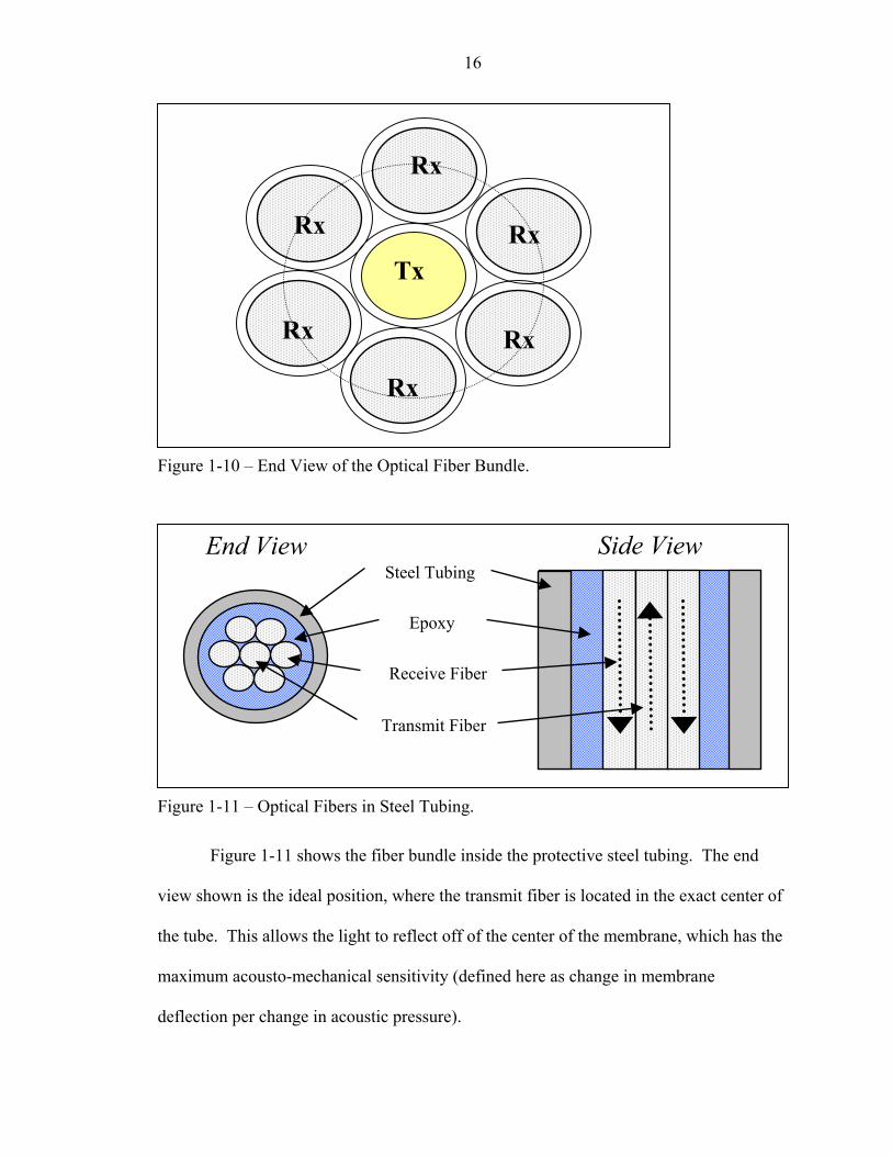
Figure 1-10 – End View of the Optical Fiber Bundle.
Figure 1-11 – Optical Fibers in Steel Tubing.
Figure 1-11 shows the fiber bundle inside the protective steel tubing. The end
view shown is the ideal position, where the transmit fiber is located in the exact center of
the tube. This allows the light to reflect off of the center of the membrane, which has the
maximum acousto-mechanical sensitivity (defined here as change in membrane
deflection per change in acoustic pressure).
Side View End View Steel Tubing
Epoxy
Receive Fiber
Transmit Fiber
Tx
Rx
Rx
Rx
Rx
Rx
Rx

17
Figure 1-12 is a diagram of the fiber bundle in its protective tubing. Connections
to other parts of the system are noted. The dashed arrows indicate the path of light
through the system. Paths three and four contain modulated data.
Figure 1-12 – Optical Fiber Bundle Drawing.
Based on the work of He and Cuomo [4], the mechano-optical (MO) stage
sensitivity, defined as change in coupled optical power per change in membrane
displacement, is maximized when a single transmit fiber is surrounded by a tightly
packed ring of receive fibers (see Figure 1-10). The smaller the radius of the receive
ring, the greater the sensitivity of the MO stage, and the smaller the equilibrium gap,
which is defined as the equilibrium distance between the fiber bundle face and the
membrane.
It may be possible to increase the sensitivity of the MO stage by adding extra Tx
fibers [16]. The current fiber bundle is designed to sample the displacement of the
membrane at the center (at the maximum displacement). For membranes which are much
larger than the accompanying fiber bundles, all bundles could illuminate areas near the
center of the membrane, where Sam is high and the stage is linear. If the diameter of the
Device
Transmit
Receive
From laser
To Detector
12
3 4
Steel Hypodermic Needle
Emitted Light (no reflecting
membrane present)

18
bundle structures is on the order of the membrane, then sensitivity gains will be lessened
and linearity of the stage may become an issue. Sensitivity and linearity are discussed
later in this thesis.
Since the MO stage sensitivity is a result of the displacement of the illuminated
region of the membrane, extra MO sensitivity can be obtained by illuminating additional
portions of the membrane by additional fiber bundle structures. With the assumptions
that adding additional identical bundle structures does not remove any light collection
ability, the same electro-optic sensitivity is available to each bundle structure, and the
region of the illuminated membrane is locally flat, then the MO stage will remain linear
and the system sensitivity would be given by the following equation.
∑=i
iammooe SSSS _ Equation 1-1
1.2.4. Light Source
The light source used by this optical microphone is the HP8168B Tuneable Laser
Source. The maximum output power of the laser at 1550 nm is 0.515 mW. An alternate
laser source or an LED source could be used in place of the HP8168B.
1.2.5. Detection Electronics
There are three schemes considered by this thesis for use as detection electronics.
The first scheme uses a single photodetector and takes the unreferenced output of the
photodetector as the microphone output. This technique is called the unreferenced output
technique. This scheme can be used with an amplifier at the output of the microphone to
increase the gain. The primary advantage of this scheme is simplicity. Fewer optical and
electronic components are required here than for any other configuration (see Section

19
5.2.1 for details). This greatly reduces the cost of the optical microphone when compared
with the other opto-electronic configurations. The largest disadvantage of this
configuration is the dependence of the unreferenced OE sensitivity on the optical power
(shown in Section 2.2.1.3). This dependence makes the unreferenced optical microphone
much less stable in the presence of laser instability and drift. Also, the overall sensitivity
of the unreferenced OE microphone is less than the referenced microphone configuration.
The second scheme, which was used by Kadirval [8], is the referenced output
technique. It uses an optical splitter to separate the light source output into two paths.
One path is connected to the Tx fiber for transmission to the MEMS chip. The Rx output
is the modulated data signal, and is taken to a photodetector. The second path is
connected directly to a photodetector for use as a reference signal. An analog divide
circuit is used to divide the modulated signal by the reference signal, and the divided
signal is taken as the microphone output. The largest advantage of the referenced output
configuration is the independence of the sensitivity on light source power. This
minimizes the negative effects of low frequency fluctuations in the light source output
power, such as fluctuations due to temperature changes. Another advantage of the
referenced output configuration is the ability to significantly improve microphone
performance by adding optical losses to the reference signal path (shown in Chapter 2).
Additionally, an amplifier may be used at the output to further increase sensitivity.
Despite the advantages, the referenced optical microphone requires more optics and
electronics than the unreferenced microphone (see Section 5.2.1 for details). This
increases the cost compared to the unreferenced microphone. Another disadvantage is

20
the increased electronics noise in the output due to the extra electrical components
(Section 2.2.4 for details).
The third scheme, heterodyne modulation, is designed to take advantage of the
flatness of the overall noise floor of the unreferenced optical microphone at high
frequencies. In this scheme, the laser output is modulated by an external sinusoidal
signal to frequencies much higher than the high frequency cutoff of the microphone. The
received optical microphone signal at the photodetector will be contained as a bandpass
signal centered at fo, where fo is much larger than the microphone bandwidth. After
passing through the photodetector, the signal is passed through a lock in amplifier and
demodulated back to the original baseband signal. This will make the noise floor of the
microphone dependant on the high frequency noise floor of the laser, and not the low
frequencies where 1/f noise (and other noise sources) is present. As with the previous
two OE configurations, an amplifier can be used at the output to increase sensitivity. The
major disadvantage of this electronic configuration is the increased electronic complexity
when compared to the other electronic configurations. Additionally, the lock-in amplifier
must be capable of passing frequencies at least 10 times the microphone high frequency
cutoff. Also, even small laser transients will cause the lock-in amp to fail to reproduce
the signal. This scheme was not implemented in this thesis, although it is likely that an
optical microphone system using a laser as the light source would require heterodyne
detection for satisfactory performance.

21
CHAPTER 2 MICROPHONE SYSTEM PARTITIONING AND PERFORMANCE METRICS
2.1. System Partitioning
The intensity-modulated optical microphone is partitioned into three stages where
transduction between energy domains occurs. The three stages of an intensity-modulated
optical microphone were identified by Bilaniuk [2]. They are the acousto-mechanical
stage, the mechano-optical stage, and the opto-electrical stage. Kadirval [8] and Bilaniuk
[2] discuss these stages in detail, and a summary is included below.
2.1.1. Acousto-Mechanical Stage
The acousto-mechanical stage is where the energy in the acoustic signal is
converted into the mechanical domain. This is accomplished when the pressure and
volume velocity of the acoustic signal induce a displacement and restoring force in the
membrane. The unit of sensitivity for this stage is a displacement per unit pressure,
typically given in µm / Pa.
2.1.2. Mechano-Optical Stage
In the mechano-optical stage, input optical power is reflected by the displacing
membrane and coupled into output (Rx) fibers. Transduction occurs when the
mechanical displacement of the membrane varies the percent of the input power that is
coupled into the output fibers. The unit of sensitivity of this stage is normalized power
per unit displacement, typically given in µm-1.

22
2.1.3. Opto-Electrical Stage
The third and final transduction stage in an intensity-modulated optical
microphone is the opto-electrical stage. This stage uses one or more photodetectors to
convert the coupled optical power into an electrical signal. The sensitivity units for this
stage are normally written as in volts (V). Occasionally an author will write the OE stage
sensitivity in V/(W/W). Most authors (including Bilaniuk) lump the optical power
dependence of the overall sensitivity of some microphone configurations into the OE
stage.
2.2. System Performance Metrics
Kadirval [8] used the following performance metrics to classify the optical
microphone. They are sensitivity, linearity, frequency response, noise floor and
minimum detectable signal (MDS). These metrics can also be used to describe the
performance of the individual stages. The theoretically determined performance metrics
for the system and each stage are summarized later in this chapter.
In this thesis, a theoretical sensitivity model for the referenced output
configuration is derived for the case where optical reference path losses and a low-noise
amplifier at the output are present. A theoretical model of the electronic noise is derived
for both unreferenced and referenced configurations. This model extends the noise
model derived by He & Cuomo [16] and used by Kadirval [8] to include the intensity
noise of the light source and all electronics. The physics behind the minimum detectable
signal equation presented by Kadirval [8] are explained, and the equation is used with the
improved noise model to predict the minimum detectable signal.

23
2.2.1. System Sensitivity
The sensitivity of a system is defined as the differential change of the output
quantity divided by the differential change of the input quantity. For a microphone, the
system output is a voltage, and the input is a pressure. The optical microphone is a multi-
energy domain system with three transduction stages, as previously described. The
maximum ideal sensitivity is a product of the sensitivities of the individual stages.
Equation 2-1 is the equation for the system sensitivity in terms of the individual stages.
All reported sensitivities in this thesis are based on a fiber bundle with identical Tx and Rx
fibers having an inner core diameter of 105 µm and a cladding diameter of 125 µm.
oemoam SSSS = Equation 2-1
Section 2.2.1.3 examines the sensitivity of the OE stage in more detail then was
done by Kadirval [8]. It derives theoretical models for the OE sensitivity in the
unreferenced and referenced configurations, and it examines sensitivity limits of the stage
resulting from the finite linearity range of the photodetector.
2.2.1.1. Acousto-Mechanical Sensitivity
The acousto-mechanical stage converts pressure to a displacement. Equation 2-2
gives the sensitivity of the stage, where wo is the deflection of the membrane at the
center, and p is the acoustic pressure at the center of the membrane.
pw
S oam ∂
∂= Equation 2-2
To derive Sam, first begin with Equation 2-3, the transverse deflection equation for
a plate derived by Sheplak et al. [17].

24
( ) ( )
( )
−
+−
−= 2
22
132
42
42112)(
ara
kkI
kIakrI
Ehkparw
ooν Equation 2-3
Figure 2-1 – Side View of Deflecting Plate or Membrane.
In the case of a membrane where a << kr, Equation 2-3 simplifies to Equation 2-4.
( )
−= 2
2
23
4
178.2ar
kEhparw Equation 2-4
Letting wo = w(0) and substituting Equation 2-4 into Equation 2-3 produces the
equation for the sensitivity of the membrane as a function of radial distance from the
center.
( )
−= 2
2
23
4
178.2ar
kEharSam Equation 2-5
If we assume that the light spot on the membrane is very small (10% or less) with
respect to the membrane diameter, then the sensitivity of the membrane can be lumped at
w(r)Equilibrium Membrane Position
Positive Plate Deflection
Negative Plate Deflection
Clamped Boundary

25
the radial center. Equation 2-6 gives the final equation for the acousto-mechanical
sensitivity of the membrane, lumped to the radial center.
( ) 23
478.20kEhaSS amam == Equation 2-6
If it cannot be assumed that the light spot is small, then the membrane sensitivity
cannot be lumped into the center of the membrane. Sam will become a function of radial
position, r, with respect to the membrane center, and the microphone sensitivity will
decrease.
In this optical microphone, the light spot illuminates less than 10% of the
membrane. Based on the observed fiber position error (see Section 3.3.1) of less than 50
µm for the fiber bundle used in this thesis, Sam can still be approximated as a constant for
this membrane.
The tension parameter k is determined by Equation 2-8. The in-plane stress (σo)
of the nitride layer for the nitride deposition process used in the microphone fabrication
was reported to range between 50 MPa and 120 MPa by the MEMS Exchange website.
Special fabrication instructions were given to minimize the in-plane stress in the nitride
layer, so it is expected that the stress will be equal to the minimum reported value for the
MEMS Exchange deposition process, σo = 50 MPa. Using E = 270 GPa (for SixNy), h =
1 µm, a = 1 mm, and νo = 0.27 (for SixNy), we estimate Sam = 1.249 x 10⁻³ µm / Pa.
( )Eh
ak oo σν 2112 −= Equation 2-7
For a discussion of the effects of the observed membrane linearity on Sam, see
Sections 2.2.2.1 and 5.3.2.

26
2.2.1.2. Mechano-Optical Sensitivity
The mechano-optical transduction stage converts a mechanical displacement to an
optical power coupling factor. The sensitivity of the stage is given by Equation 2-8,
where w is the deflection of the membrane at the center, and η is the coupled optical
power of the stage in W/W.
wSam ∂
∂=
η Equation 2-8
He and Cuomo [18] derived a formula for determining the power coupled by
light reflecting off of a deflecting membrane in a microphone similar to that shown in
Figure 1-8. The analysis is valid for multimode optical fibers. Theoretical work by Ruan
and Felson [19] can be used to derive the power coupled as a function of membrane
displacement for the case of a single mode transmit fiber and a multimode receive fiber,
although that configuration is not analyzed here. Ruan and Felson’s work is applicable to
membranes with a finite radius of curvature, however He and Cuomo’s work is not. The
analysis here based on [18] assumes no misalignment errors and no power lost due to
mismatch between fiber numerical apertures (NA). This is a good approximation when
the angular alignment between the fiber surface and the membrane is less than 5 degrees
(for fibers with NA = 0.22 or less). If this approximation does not hold, then the method
of images (explained below) is not valid. Adjusting the method of images to account for
angular alignments is complicated, and as of this writing, no work exists that rigorously
solves the problem. Section 3.3.1 discusses types of alignment errors, methods to avoid
them, and their implications in more detail.

27
In general, the power coupled into an optical fiber can be determined by
integrating the optical intensity (also known as the irradiance) over the collecting surface,
assuming all light present is entering the fibers at an angle less than the acceptance angle
of the fiber. If this is not the case, then only the irradiance due to rays entering the fiber
at less than the acceptance angle should be integrated in Equation 2-12. The analysis of
He and Cuomo [18] assumes the former. The reflected intensity profile at the surface of
the fiber bundle is determined in [18] by the method of images.
Figure 2-2 – Method of Images (View from Side of Fiber Bundle).
In the method of images, the reflecting surface is defined to be the reflecting
plane, and the surface of the fiber bundle (as shown in Figure 1-10) is defined to be the
receiving plane. They are separated by a gap, g. The method of images states that the
reflected optical power incident onto the Rx cores is the same as the optical power
incident on the Rx core images, located at a distance of 2g from the receiving plane.
Image Plane Reflecting Plane Receiving Plane
Transmit Fiber Core
g g
Receive Fiber Core
Receive Fiber Core
Rx Fiber Image
Rx Fiber Image

28
Using the method of images, He and Cuomo derived an equation for the intensity
on the image plane as a function of radial distance from the center of the fiber bundle.
This thesis uses Equation 2-9 through 2-11 from He and Cuomo [18] as the first step in
determining the power coupled and sensitivity of the MO stage. Without an
understanding of these equations, a microphone designer will not be able to identify
miscalculations due to errors that have been observed in the output of Equation 2-9. This
problem will be discussed in more detail later in this section.
Equation 2-9
The quantity, A, used in Equation 2-9 is defined by Equation 2-10. In Equation 2-
10, rtx_core is the radius of the transmit fiber core, and g is the equilibrium gap.
gr
A coretx
2_= Equation 2-10
( ) ( ) ( )( ) ( ) ( )
( ) ( ) ( )( ) ( ) ( )( ) ( ) ( )
( ) ( ) ( )( ) ( ) ( )( )
( ) ( ) ( )
( ) ( ) ( )( ) ( ) ( )( )
( ) ( ) ( )
( ) ( ) ( ) ( )( ) ( )( ) ( ) ( )
( ) ( ) ( )( ) ( ) ( )( )
( ) ( ) ( )
( ) ( ) ( )( ) ( ) ( )( )
( ) ( ) ( )
( ) ( )( )( ) ( )[ ] ( ) ( ) ( )
( ) ( )( )( ) ( )( ) ( ) ( ) ( )
>−>>
++−−++
≤−>>
−+−++−
>−≤≤≥
++++
+
−+−−−
−
≤−≤≤≥
−++−
+
−+−−−
−
≤<<≤−−−+−−−−
>−<≤>
++++
+
−−−+−
−
≤−<≤>
−++−
+
−−−+−
−
≤<−<≤−−−+−−−−
−≤≤<≤−−−−
=
−−−
−−−
−−−−
−−−
−−−
−−−−
−−
2&2&2111111ln
8
2&2&2111111ln
8
2&21&211
11ln8
1tan1tantan412
2&21&211
11ln8
1tan1tantan412
1&211tan1tan1tan1tan12
2&10&211
11ln8
1tan1tantan412
2&10&211
11ln8
1tan1tantan412
12&211tan1tan1tan1tan12
20&211tan1tan1
)(
222
222
222
222
22
22111
2
22
22111
2
11112
22
22111
2
22
22111
2
11112
112
kkkkifkAkkAkA
kkkkifkAkkAkA
kkkkifkA
AkAkAAkAAA
A
kkkkifkA
AkAkAAkAAA
A
kkkifkAAkAAkkA
A
kkkkifkA
AkAkAAkAAA
A
kkkkifkA
AkAkAAkAAA
A
kkkifkAAkkAAkA
A
kkkifkAAkAA
IrI
ccc
ccc
c
c
cccc
ccc
c
cc
ccccc
cccc
ccc
c
cc
ccccc
cccc
o
θ
θ
θπ
θ
θπ
θ
θ
θπ
θ
θπ
θ
θ
θ

29
The quantity k used in Equation 2-9 is defined by Equation 2-11. In Equation 2-
11, rtx_core is the radius of the transmit fiber core, and r is the radial coordinate measured
from the center of the Tx fiber axis.
coretxrrk_
= Equation 2-11
The quantities θc and kc are the critical angle of the Tx fiber and the critical value
of k associated with that angle. For more details on the variables, see He and Cuomo’s
work [18].
Some sets of input parameters with a gap, g, on the order of the Tx fiber diameter
were observed to produce non-intuitive intensity profiles. For example, using Equation
2-9 at a gap of 50 µm with a Tx fiber core diameter of 105 µm resulted in I(r) = 0 at all
values of r. Therefore, for the theoretical power coupled and sensitivity to be accurate, an
optical microphone designer must plot Equation 2-9 for equilibrium gaps of the desired
value. If the plots are erroneous, then the power coupled and sensitivity analysis will be
invalid. The Mathcad code used to generate the intensity curves was carefully examined
for errors, and none were found. It is possible that Equation 2-9 does not accurately
predict the intensity at small gap distances.
The power coupled into the receive fibers is determined by using a ring
approximation with a power correction factor. The ring approximation used in He and
Cuomo [18] approximates the face of the receive fibers as an annular ring. The power
coupled is determined by integrating the normalized intensity (Equation 2-9) over the
ring area. Figure 2-3 shows the ring approximation. The actual light collection surfaces

30
are shaded gray, and the integrated area of the ring approximation is shown by the dashed
ring. Note that the relative sizes of the core and claddings are not necessarily to scale.
Figure 2-3 – Ring Approximation Diagram.
The power coupled and sensitivity equations for the mechano-optical (MO) stage
are given by He and Cuomo [18]. These were the equations used by Kadirval [8] to
predict the performance of the MO stage in his optical microphone. This thesis has
modified the power coupled equation from [18] (referred to as the ideal power coupled
from this point) to include the effects of radial position errors in the receive optical fibers,
and also to correct for overestimation of the power coupled by the ring approximation.
Radial position error, RPE, is defined and discussed in Section 3.3.2. The power
coupled correction factor, cf, is calculated by taking the ratio of the actual surface area of
the receive fibers to the area of the ring in the ring approximation. The ideal power
coupled is then multiplied by this correction factor (which is a function of the optical
fiber geometry and the RPE) to calculate the corrected power coupled. In this thesis,
ideal power coupled and sensitivity refers to the case where cf = 1, meaning that the ring
approximation area exactly matches the surface area of the receive fibers. Since this can

31
never happen in practice, the ideal situation will occur only when the area mismatch is
neglected, as is done by [18] and [8]. The corrected power coupled and sensitivity
equations are given in Equations 2-12 and 2-13.
( ) ( ) ( ) kdkI
gkIRPEcPP
RPEgcoretx
RPEb
coretxRPEm o
f
i
o ⋅== ∫+
+−
σπ
η_
_1
,2, Equation 2-12
( ) ( )( )RPEgdzd
PP
dzdRPEgS
i
omo ,, η=
= Equation 2-13
Two theoretical corrected power coupled curves, based on using Equation 2-12
with a fiber bundle constructed from AFS105/125Y multimode fibers as both Tx and Rx,
are shown in Figure 2-4. One of the curves corresponds to an RPE of 0 µm, and the other
corresponds to an RPE of 10 µm (the observed RPE of the custom fiber bundle). The
corresponding corrected sensitivity curves are shown in Figure 2-5. The horizontal axis
on each plot is the equilibrium gap, g, between the receiving plane and the reflecting
plane in the method of images.
The maximum corrected theoretical MO sensitivity with RPE = 0 µm is Smo =
1.094E-3 µm-1 and occurs at g = 230 µm. When the power coupled correction factor is
taken into account, the maximum corrected theoretical power coupled is Smo = 0.784E-3
µm-1 and occurs at g = 265 µm.

32
0%
5%
10%
15%
20%
25%
30%
0 100 200 300 400 500 600 700 800 900 1000
Gap (um)
Pow
er C
oupl
ed (W
/W)
RPE = 0 um RPE = 10.0 um Figure 2-4 – Theoretical Power Coupled with Ideal Fiber Configuration.
-4.00E-04
-2.00E-04
0.00E+00
2.00E-04
4.00E-04
6.00E-04
8.00E-04
1.00E-03
1.20E-03
0 100 200 300 400 500 600 700 800 900 1000
Gap (um)
Sens
itivi
ty (1
/ µm
)
RPE = 0 um RPE = 10 um Figure 2-5 – Theoretical Sensitivity with Ideal Fiber Configuration.

33
The discontinuities observed in the sensitivity equations are due to transitions in
the power coupled integral. Specifically, each discontinuity corresponds to the edge of
the light cone crossing the boundary of the receive fiber ring. The discontinuity is
present in the power coupled equations, but since it manifests in these plots as an integral
of the discontinuity seen in the sensitivity curves, it is difficult to see on the viewing scale
of the power coupled plot.
2.2.1.3. Opto-Electrical Sensitivity
The opto-electrical stage converts an optical power coupled to an electrical signal.
This is accomplished with the use of a Thorlabs PDA400 photodetector, which consists
of a photodiode and a trans-impedance amplifier with five gain settings. In this thesis,
the photodiode and trans-impedance amplifier are collectively referred to as a
photodetector, and they are treated as one unit.
The sensitivity of the stage is given by Equation 2-14, where η is the optical
power coupled, and V is the output voltage of the sensor.
ηddVSoe = Equation 2-14
The output voltage of the opto-electrical stage is a function of the detection
electronics and the detection method used. For the Unreferenced Output detection
technique, shown in Figure 2-6, the output voltage is a function of the photodetector
responsivity and gain, the output amplifier gain, and the laser power.

34
Figure 2-6 – Block Diagram of the Unreferenced Output Configuration.
The output voltage of the unreferenced output configuration, Equation 2-15, is
derived by applying Kirchoff’s and Ohm’s Laws to the equivalent circuit of the detector,
shown in Figure 2-7. Since a voltage amplifier is connected in series with the detector,
the output amplifier gain, Ga, is multiplied by Vdet_out to get the microphone output
voltage, Vout. Pout is the received optical power from the fiber bundle Rx fibers. By
equating Pout with η times Pin, Equation 2-15 neglects losses in the fiber bundle other than
those from the power coupling effect. For a real bundle, other losses are present at the
connectors and in the fibers themselves. These losses have not been measured and are
neglected here.
ηinaoutaout PRGGPRGGV == Equation 2-15
PhotodetectorLowpass Filter /
Output Amplifier
Photodiode Trans-impedance Amplifier
Pout Vout R G Ga

35
Figure 2-7 – Equivalent Circuit for the PDA400 Photodetector.
Substituting Equation 2-16 into Equation 2-15 gives the equation for the electro-
optical sensitivity of the Unreferenced Output detection technique.
inaoe PRGGS = Equation 2-16
Equation 2-16 shows a linear relation between the received optical power and the
OE stage sensitivity. This linear relationship only holds when the photodetector is
operated in a linear region. A Thorlabs PDA-400 photodetector, with specs given in
Appendix D, has a peak response of 0.95 A/W at 1550 nm. The minimum trans-
impedance gain setting, G, for the PDA400 is 15,000 V/A. Using the detector response R
= 0.95 A/W and the gain G = 15000 V/A, gives Soe = 14250(V/W)*Pin. If Pin = 0.7 mW,
then Soe = 9.975 V. Since the photodetector saturates at 10 V, the maximum
unreferenced OE stage sensitivity is 9.975 V * Ga.
It is very important to observe that the overall sensitivity of the unreferenced
optical microphone is limited by the maximum DC optical power received by the
photodetector due to detector saturation. Ideally, the photodetector would consist of only
-+
Pout R Pout Gdet
+ -
Vdet_out
Photodiode Trans-impedance Amplifier
36
a photodiode, and a highpass filter would be placed at the photodiode output. Without
the trans-impedance amplifier, the DC optical power can be removed before
amplification, eliminating the limit of the OE sensitivity due to the DC optical power.
Any sensitivity lost from removing the trans-impedance amplifier can be recovered by
increasing the gain of the output amplifier.
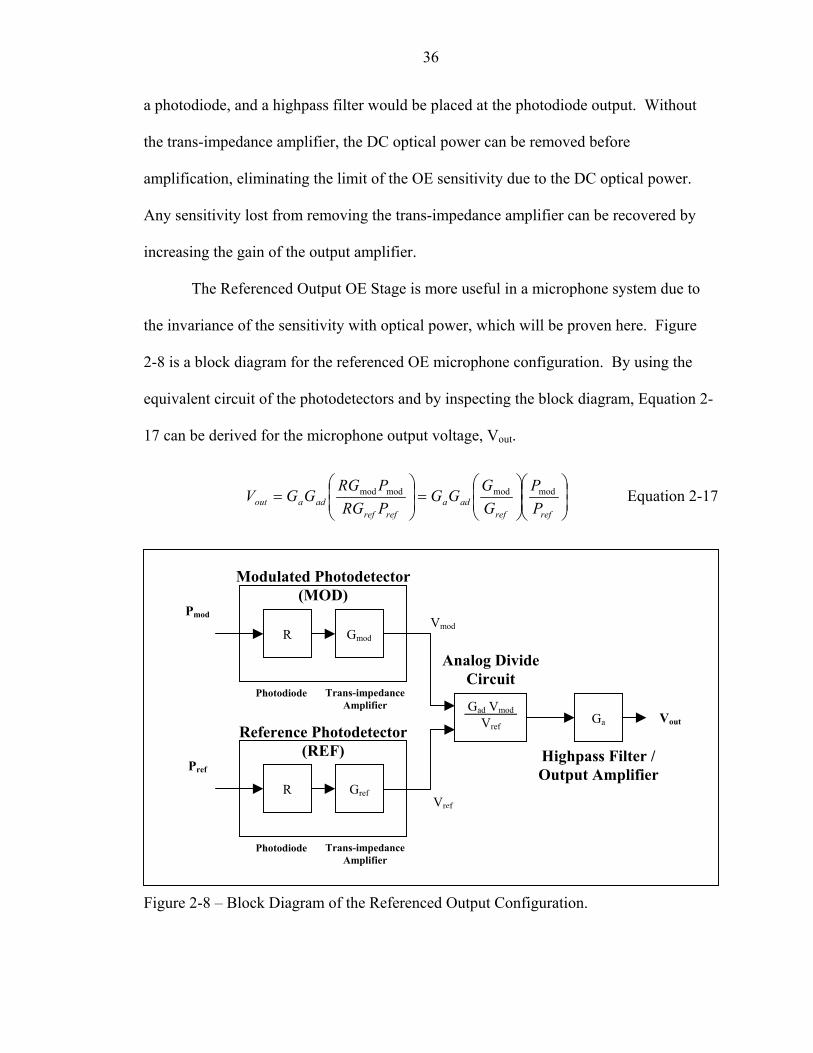
The Referenced Output OE Stage is more useful in a microphone system due to
the invariance of the sensitivity with optical power, which will be proven here. Figure
2-8 is a block diagram for the referenced OE microphone configuration. By using the
equivalent circuit of the photodetectors and by inspecting the block diagram, Equation 2-
17 can be derived for the microphone output voltage, Vout.
=
=
refrefada
refrefadaout P
PGG
GGPRGPRG
GGV modmodmodmod Equation 2-17
Figure 2-8 – Block Diagram of the Referenced Output Configuration.
Highpass Filter / Output Amplifier
Vout
Modulated Photodetector (MOD)
Photodiode Trans-impedance Amplifier
Pmod
R Gmod
Ga
Photodiode Trans-impedance Amplifier
Pref
R Gref
Analog Divide Circuit
Gad Vmod
Vref Reference Photodetector (REF)
Vmod
Vref

37
In Equation 2-17, Pmod is identical to Pout in the unreferenced block diagram, when
the same assumptions are made. If α is the optical losses present in the reference signal
path, then Pref can be represented as (1- α) Pin. By observing that the fiber bundle power
coupled, η, is Pout / Pin, Equation 2-17 can be rewritten in terms of the component gains
and the optical power coupled into the fiber bundle.
( ) ηα
−=
ref
adaout G
GGGV mod
1 Equation 2-18
Substituting Equation 2-18 into Equation 2-15 gives the equation for the electro-
optical sensitivity of the Referenced Output detection technique, where Gratio is the ratio
of Gmod to Gdet.
( ) ( ) ( )ratioada
ref
adaoe G
GGGGGG
Sαα −
=
−=
11mod Equation 2-19
Equation 2-19 varies directly with the ratio of the modulated detector gain to the
reference detector gain (Gmod / Gref), with the built-in gain of the analog divide circuit
(Gad), and with the gain of the output amplifier (Ga). Also, increasing optical losses in
the reference path, α, increases the sensitivity of the OE stage and decreases the optical
power incident on the photodetector. Later in this chapter, it will be shown that optical
reference path losses will improve the electronics noise and microphone minimum
detectable signal under some conditions.
Using two PDA-400 photodetectors, an analog divide circuit hardwired for a gain
of 10 V, and the minimum and maximum values of Gratio (based on available PDA400
gains settings), the sensitivity of the OE stage can range between Soe_min = (0.10 V)*Ga /

38
(1-α) and Soe_max = (1000 V)* Ga / (1-α). If we take the ratio of the sensitivity of the
referenced to the unreferenced OE stage, we can see how the stage sensitivities compare
at varying input power levels. This is done in Figure 2-9 for Gad = 10 V and Ga = 1 V /
V.
From Figure 2-9, it can be concluded that the unreferenced microphone will have
a lower sensitivity than the referenced microphone unless the laser is operated at the
maximum power for which the photodetector remains linear, no reference path losses are
present, and the photodetector gain ratio is one. When this occurs, the two stages will
have identical sensitivities. Increasing Gratio and α will increase the sensitivity of the
referenced OE stage. These values are physically limited by the photodetector range of
linearity for Gratio and α, and also by the analog divide circuit for α. Specifically, the
input to the analog divide circuit must never drop below a certain threshold, and the
output of the analog divide circuit can never saturate. This limits α to less than 0.9 for
the AD circuit used in this thesis. In practice, the PDA400 detectors are not useful when
the gain is set higher than 47,000 V/A. An additional constraint is the fixed gain-
bandwidth product limiting the maximum gain for a minimum bandwidth.

39
0
1
2
3
4
5
6
7
8
9
10
0 100 200 300 400 500 600 700
Laser Power (µW)
S oe_
ref /
Soe
_unr
ef
Gratio = 1, Gdet = 15000 V/A, Alpha = 0Gratio = 3.1, Gdet = 15000 V/A, Alpha = 0Gratio = 1, Gdet = 15000 V/A, Alpha = 0.5
Figure 2-9 – Comparison of Unreferenced and Referenced Output Sensitivities.
2.2.2. System Linearity
The linearity of the optical microphone is determined by the linearity of the
individual stages. The acousto-mechanical stage linearity is governed by the nitride
membrane. The linearity of the mechano-optical stage is dominated by the assumptions
that the membrane curvature is negligible, and by the local flatness of the sensitivity vs.
equilibrium gap curve. The linearity of the opto-electrical stage is governed by the
linearity range of the photodetector and additional electronics. The following sections
establish the conditions for linearity of each stage, and therefore the whole device.

40
2.2.2.1. Acousto-Mechanical Linearity
The theory for the range of linearity of the membrane was investigated by
Sheplak and Dugundji [20]. Using this theory, Sahni et al. [21] determined that the
diaphragm is linear over the region from 0 – 2000 Pa (160 dB re. 20 µPa). Sheplak et al.
[20] present Equation 2-20, which relates the membrane aspect ratio to the in-plane stress
and the maximum linear pressure (3% linearity).
Epha o
max
23
max
σ=
Equation 2-20
By substituting the maximum linear pressure and the microphone membrane
dimensions into Equation 2-20, the in-plane stress, σo, of the membrane can be estimated.
The experimental linearity range of the microphone (see Chapter 5) is reached at 122 dB
(re. 20 µPa). This results in the AM sensitivity increasing by a factor of 15. This effect
is considered when predicting the microphone performance in Section 2.2.7.
2.2.2.2. Mechano-Optical Linearity
The linearity of the mechano-optical stage is based on two factors: the linearity of
the power coupled curve (flatness of the sensitivity curve), and the assumption of the
membrane curvature being negligible.
The point of interest for the linearity analysis is about the point of maximum
sensitivity. Figure 2-10 shows a plot of the sensitivity from an equilibrium gap of 240
µm to 290 µm using Equation 2-13. The vertical axis of the curve is highly magnified,
and the thin horizontal lines denote the region that is within 3% of the maximum
sensitivity. It is evident from Figure 2-10 that the MO stage sensitivity is linear within

41
+/-10 µm of the optimal gap. Since the largest maximum membrane deflection, at Pmax =
2 kPa, allowed by the variability in the nitride stress of the MEMS chip process is +/-2.49
µm, the sensitivity of the MO stage will be constant within 3%. The large window for
linearity holds at equilibrium gaps out to 400 µm. This means that if the equilibrium gap
is set at a value larger than the best case equilibrium gap, then the sensitivity will still be
constant to within 3% over the range of the diaphragm motion.
5.00E-04
6.00E-04
7.00E-04
8.00E-04
9.00E-04
1.00E-03
240 245 250 255 260 265 270 275 280 285 290
Gap (µm)
Cor
rect
ed T
heor
etic
al S
ensi
tivity
(1 /
µm)
Figure 2-10 – Linearity of Mechano-Optical Stage.
The second criterion for establishing the linearity of the MO stage is the flatness
of the membrane over the illuminated region. An alternate way of viewing this
requirement is to look at the acousto-mechanical sensitivity of the membrane over the
illuminated region as a function of radial distance from the center. For linearity, the MO
sensitivity of the membrane should vary by no more than 3%. It is important to note that
the method of images used in Section 2.2.1.2 requires a flat membrane in the illuminated

42
area. This means that the membrane must be within 3% of planar over the illuminated
region, and must be parallel to the fiber bundle face.
Figure 2-11 shows the normalized acousto-mechanical sensitivity, using Equation
2-6, of the membrane as a function of the radial distance from the membrane center. This
plot shows that the sensitivity is within 3% of the maximum when the illuminated area is
within 93 µm of the membrane center. For optical fibers with an NA = 0.22, the spot
radius is less than 93 µm when the gap is less than 430 µm.
0.76
0.84
0.92
1.00
1.08
1.16
1.24
0 10 20 30 40 50 60 70 80 90 100
Radial Distance from Membrane Center (µm)
Nor
mal
ized
Aco
usto
-Mec
hani
cal S
ensi
tivity
Figure 2-11 – Plot of Acousto-Mechanical Sensitivity as a Function of Radial Position.
It has been determined that the MO stage sensitivity varies by no more than 3%
over the equilibrium gap range of 200 µm to 400 µm. It has also been determined that
the acousto-mechanical sensitivity at every illuminated point on the membrane is within
3% of its maximum value when the equilibrium gap is less than 430 µm. Therefore, the
MO stage of the optical microphone is linear when the equilibrium gap is between 200

43
µm and 400 µm. Since the ideal equilibrium gap is 230 µm, the OM stage of the optical
microphone is linear at the equilibrium gap of 230 µm with a maximum deflection of +/-
2.49 µm at Pmax = 2 kPa.
This analysis does not include the effect of misalignments on the linearity. They
are discussed in Chapter 3.
2.2.2.3. Opto-Electrical Linearity
The linearity of the opto-electrical stage is effectively limited by the linearity of
each electronics component in the system. The PDA-400 photodetectors are linear up to
an output voltage of 10 V. The AD734 analog divide chip is linear over the input range
of +/- 12.5 V. Therefore, the photodetectors are the limiting factor in determining the OE
stage linearity. As long as the detectors are operated below saturation, the opto-electrical
stage is linear.
The maximum voltage that can be output in the linear range of operation for the
electronics serves to limit the maximum sensitivity of the unreferenced output
configuration when the output amplifier is held at a fixed gain. To illustrate, consider
Equation 2-21, the equation for the photodetector output in terms of the optical power for
the unreferenced OE configuration.
laserout RGPV = Equation 2-21
The maximum Vout that the PDA400 photodetector can output is 10 V. The
responsivity is 0.95 A/W. Substituting these constants into the above equation shows that
the product of the gain and the optical power cannot be larger than the saturation voltage
of the detector divided by the detector responsivity, or 10.5 W*V / A for the PDA400.

44
This product effectively limits the maximum sensitivity that the unreferenced OE stage
can provide, since increasing Plaser requires G to be reduced if Plaser*G > 10 V. When the
range of linearity of the measurement equipment is considered, then the gain of the
output amplifier is also limited. To ensure the microphone can operate in its intended
environment, the linearity range of the measurement equipment must also be considered.
2.2.3. System Frequency Response
The frequency response of the optical microphone was discussed in depth by
Kadirval [8]. He developed an equivalent circuit for each stage of the optical
microphone. The frequency response of the microphone is the product of the frequency
response of the individual stages.
2.2.3.1. Acousto-mechanical frequency response
The lumped element model parameters used in the acousto-mechanical stage are
shown in Table 2-1. These parameters were given by Sahni [21]. The frequency
response analysis for this optical microphone membrane was presented by Kadirval [8],
and it remains valid. Using the lumped element parameters in Table 2-1 and the
equations for the frequency response of the AM stage, the 3 dB frequency for the upper
end of the frequency response was 76.25 kHz. The lumped element approximation ia
limited to below 50 kHz according to Sahni [21], so the upper limit of the frequency
response will not be accurately predicted by this model.
( )( )22
_
131 sCMa
CsH
effeff
effunormam
+=
π Equation 2-22

45
( ) ( )( )HzjH
sHsH
normam
normamnormam 02_
__ π
= Equation 2-23
Table 2-1 – Acousto-Mechanical Lumped Element Parameters
Parameter Formula Value Units
Mmea 23 ahn
⋅πρ
1316 kg / m4
Cmea ha
o ⋅⋅
σπ2
4
1.963E-15 m3 / Pa
Mrad 23 aa
⋅πρ
5.199E+5 kg / m5
Ca 2
2
cha
a
cav
ρπ ⋅
1.246E-15 m3 / Pa
fres n
o
a ρσ39.0 98.6 kHz
The lower end of the frequency response is governed by the vent channel of the
microphone. Although the optical microphone was not designed with a vent channel, the
steel tube is not an exact fit with the membrane cavity, and allows equalization of the
pressure on both sides of the membrane due to low frequency pressure fluctuations.
2.2.3.2. Mechano-optical frequency response
The mechano-optical frequency response is a constant. This was discussed by
Kadirval [8] in detail, and will not be reproduced here.
2.2.3.3. Opto-electrical frequency response
The opto-electrical frequency response is determined by the frequency response
of the electrical components in the system. The photodetector has a worst case
bandwidth of 50 kHz at the maximum gain and a bandwidth of 10 MHz at the lowest
gain. The analog divide circuit has a bandwidth of 10 MHz. Therefore, the bandwidth of

46
the photodetectors is the limiting electrical component for the upper range of the
frequency response for practical gain settings.
The lower range of the frequency response is limited by the cut-on frequency of
the highpass filter. In the highpass filter used by this thesis, the cut-on frequency was set
at 30 Hz.
2.2.4. System Electronic Noise
The electronic noise is defined to be the noise, in volts, seen at the output of the
microphone circuit. Previous works (He & Cuomo, 1991 [16], [22]) assume that “the
light source does not contribute significantly to the (noise) background.” He and Cuomo
note that these conditions do not always hold, and that voltage fluctuations due to light
source noise may affect the signal. This thesis includes the effects of the detector, the
light source intensity noise, and the electronics to determine the electronic noise at the
microphone output. The noise analysis traces the path of RMS noise signals, in V / Hz½,
through both the referenced and unreferenced electronics.
The goal of the first part of the electronics noise analysis is to identify and derive
equations for the individual noise sources that contribute to the electronics noise of the
photodetector.
Figure 2-12 – Noise Contributions for the Photodetector Output.
Photodetector
Pdet_NEP, Plight_noise R*G
Vdet, Vlight
Photodiode NEP Terms Photodetector Electronics Noise Terms

47
Figure 2-12 illustrates the noise sources that produce electrical noise at the output
of the photodetector. Pdet_NEP is the noise equivalent power at the input of the photodiode
due to the inherent noise of the photodiode (dominated by thermal and shot noise
…equations presented are referenced to Wilson and Hawkes [23]). The units for Pdet_NEP
are W / Hz½. From this point on, the photodetector output due solely to Pdet_NEP is
referred to as the detector (or photodetector) electronics noise, Vdet, and has the units V /
Hz½. Thermal noise and shot noise are the dominant noise sources in a photodetector.
The shot noise, Vshot, in V / Hz½, is given by Equation 2-24, where G is the trans-
impedance gain, R is the diode responsivity, e is the charge of an electron, and Plight is the
incident optical power received by the detector.
2shot lightV G eRP= Equation 2-24
Thermal noise, Vtherm, is also present in a photodetector, and can be given by the
following equation, where k is Boltzman’s constant, T is the mean temperature in Kelvin,
and G is the trans-impedance gain.
4thermV kTG= Equation 2-25
The total detector noise, Vdet, can be written as the RMS sum of the thermal and
shot noise, shown in the following equation.
2 2det shot thermV V V= + Equation 2-26
The other noise source, Plight_noise, represents the noise power fluctuation incident
on the photodetector due to fluctuations in the intensity of the light source integrated over
the diode collection area. The units for Plight_noise are W / Hz½. The voltage fluctuations

48
at the output of the detector produced by Plight_noise are referred to in this thesis as the light
source (or laser) electronics noise, Vlight. The units are the units V / Hz½. Where
necessary, subscripts will be added to distinguish between referenced and unreferenced
quantities. Since Plight_noise is highly dependant on the type of light source and supporting
electronics, a purely theoretical model will not be used (see the end of this section).
Instead, the electronics noise at the output of the photodetector will be measured. The
measured quantity will be equal to the RMS sum of Vlight_noise and Vdet. By using
Equations 2-24 – 2-26 and the experimentally measured noise quantity, Vlight_noise can be
determined for the light source – detector system. When Vlight_noise is known, the
photodetector equivalent circuit can be used to calculate Plight_noise. Dividing Plight_noise by
the photodiode active area produces an estimate of the light source intensity noise.
Figure 2-13 – Noise Contributions for the Microphone Output.
The second part of the electronics noise analysis propagates Vdet through the
unreferenced and referenced configurations to determine the electronics noise at the
output of the microphone. These noise terms are referred to as the “total electronics
noise” or the “microphone electronics noise” terms. The total electronics noise is
determined by the amplification of Vdet by signal amplification components and the
addition of any additional electronics noise sources (see Figure 2-6 and Figure 2-8). For
Microphone OE Stage
Pdet_NEP, Plaser_noise Unref / Ref
vnoise_ref, vnoise_unref
Photodiode NEP Terms Microphone Electronics Noise Terms

49
this work, the analog divide IC used by the referenced configuration was the Analog
Devices AD734 [24].
The electronics noise analysis of the unreferenced microphone configuration in
Figure 2-6 is not difficult since only one signal path exists. By inspecting Figure 2-6,
Equation 2-27 and 2-28 can be derived for the total noise output at the photodetector,
Vdet_total and the unreferenced noise, Vunref. In Equation 2-28, Va is the input noise of the
amplifier, in V / Hz½.
( )22det_ det det _total light noiseV V RG Pη= + Equation 2-27
2 2det_unref a total aV G V V= + Equation 2-28
The analysis of the referenced microphone noise is more complicated. There are
two signal paths into the system, and a time-domain division. To complicate matters, the
optical noise Vlight_noise in the modulated and reference signal paths (see Figure 2-8) may
or may not be correlated. In a real microphone system, it is expected that the optical
noise in the modulated and reference signal paths will be correlated to some degree.
Theoretical models are presented here for both uncorrelated and correlated optical noise
in the referenced configuration.
Vlight_noise_ref and Vlight_noise_mod are given by Equations 2-29 and 2-30, which are
derived from the power to voltage conversion equations of a photodetector.
( )_ _ _
12light noise ref ref light noiseV RG Pα−
= Equation 2-29
_ _ mod mod _2light noise light noiseV RG Pη= Equation 2-30

50
When Vlight_noise_ref and Vlight_noise_mod are uncorrelated, they will not divide in the
analog divide circuit. Instead, they add as shown in Equation 2-31 for the uncorrelated
analog divide circuit output, Vad_uncorr. In Equation 2-31, Vad is the input noise of the
analog divide circuit.
2 2 2 2_ det _ _ _ _ mod2 2ad uncorr ad light noise ref light noise adV G V V V V= + + + Equation 2-31
The total electronics noise at the output of the referenced microphone for the
uncorrelated case can be determined by propagating Vad_uncorr through the output
amplifier, with input noise Va, as shown in Equation 2-30.
2 2_ _ref uncorr a ad uncorr aV G V V= + Equation 2-32
When the optical noise is correlated, then it will be divided by the analog divide
circuit. In this case, Vad_corr is given by Equation 2-32.
2
_ _ mod2 2_ det
_ _
2 2 light noisead corr ad ad
light noise ref
VV G V V
V
= + +
Equation 2-33
The total electronics noise at the output of the referenced optical microphone
when the optical noise is correlated can be determined by replacing Vad_uncorr with Vad_corr
in Equation 2-32. Equation 2-34 gives this result.
2 2_ _ref uncorr a ad corr aV G V V= + Equation 2-34
Theoretical models for the intensity noise of a laser are inaccurate in predicting
the performance of a commercial laser, due to the uncertainty in the laser quantum
efficiencies, and the variation in the performance of the electronics controlling and

51
cooling the laser. Coldren and Corzine [25] present Equation 2-41 for the relative
intensity noise, RIN, of a laser source at the optical resonance frequency (corresponding
to the laser output wavelength). The dampening factor, γ, is defined as Kf2R + γο, and is
not a parameter provided by a laser manufacturer. Experiments can be performed to
quantify it, but these are not practical to do when the direct measurement of the optical
noise PSD will provide the needed value.
( )γ
νπ ST
fRIN ∆
=∆
16 Equation 2-35
In order to make an accurate estimate of the light source noise, this thesis does not
rely on Equation 2-41. The results of the experimental measurements for Plight_noise and
Vdet are given in Chapter 5.
2.2.5. System Minimum Detectable Signal
The minimum detectable signal is the smallest signal that can be resolved by the
microphone. The minimum detectable signal is a function of physical interactions
between noise sources and desired signals in each stage as well as the sensitivities of each
stage. Previous work (He & Cuomo, 1991 [16]) only considered the OE Stage MDS, and
also ignored the laser noise effect on the total electronics noise. This work takes
additional noise sources into consideration (see Section 2.2.4).
Equation 2-42 gives the System MDS for the optical microphone. Three physical
MDS reducing mechanisms are considered: membrane noise due to the Brownian motion
of the membrane atoms, variations in the coupled laser power due to laser intensity noise
in the MO stage, and electronic noise in the OE stage. Each of these terms will be
discussed in more detail later in this section.

52
2_
22
light noise
light oer
am mo
PP VMDS p f
S S S
= + + ∆
Equation 2-36
The first term under the radical in Equation 2-42 is the AM stage MDS due to the
Brownian noise of the membrane, given in Pa2. The second term is the MO stage MDS,
which is due to the variations in the coupled laser power due to laser intensity noise, in
the presence of variations due to desired membrane deflection (from an acoustic signal),
given in Pa2. If the laser intensity noise is close in magnitude to the change in coupled
power in the Rx fiber, then the signal can never be distinguishable from the optical noise,
even with an ideal (no-noise) detector. The third term is the MDS of the OE stage, also
given in Pa2. The OE stage MDS is determined by the total electronics noise and the
measurement bin width. In previous works, the MO MDS was neglected [16, 22]. No
previous work takes the light source electronics noise into account when calculating the
OE MDS; they only consider the photodiode shot noise.
2.2.5.1. Acousto-Mechanical Minimum Detectable Signal
The dominant noise source of the AM stage is the Brownian motion of the
membrane. The silicon nitride membrane atoms, like all atoms above absolute zero,
exhibit Brownian motion. This Brownian motion causes a deflection of the diaphragm in
the same manner that an acoustic signal does. Due to this deflection, pressures which
cause a deflection smaller than the deflection due to Brownian motion are not detectable.
The equation for the mean equivalent pressure fluctuations due to the Brownian motion is
given by Equation 2-43 from Chau and Wise [26].

53
( )1 1 2 222
32r
m p m pkTp fa
απ
+= ∆ Equation 2-37
Using α = 1, T = 300 K, k = 1.38 E-23 J / K, m1 = m2 = 4.78 E-26 kg, p1 = p2 =
101.4 kPa, and a = 500 µm, the mean equivalent pressure fluctuations due to Brownian
motion is <pr2> = 3.642 E-11 Pa2 ∆f. This corresponds to a MDS of -11 dB (re. 20 µPa).
Based on the MDS of the other stages (presented later), it can be concluded that this noise
source is completely negligible in an intensity-modulated optical microphone.
2.2.5.2. Mechano-Optical Minimum Detectable Signal
The dominant noise source in the MO stage is the intensity noise of the light
source. The physical effect is illustrated in Figure 2-14. Power is coupled by light
reflecting into the receive fibers from the membrane. This power can be written as the
sum of three components: the optical DC component (Plight), the acoustically-modulated
optical power signal (Pmodulated(t)), and the optical noise power (Plaser_noise(t)).
Figure 2-14 – Illustration of the Physics Behind the MO MDS.
When the membrane deflects due to an acoustic signal, Pmodulated(t) is produced.
Fluctuations in the light power output superimposes Plight_noise(t) onto the desired
modulated signal. If the fluctuations in power coupled due to light output noise are larger
than the fluctuations in power coupled due to the acoustic signal (Plight_noise(t) >=
Time Variance of Coupled Power Components
Plaser + Plight_noise(t) + Pmodulated(t) Rx Fibers (more than one)

54
Pmodulated(t)), then the microphone will not be able to detect the acoustic signal without the
optical noise removed by the electronics. In the event that the optical noise can be
removed by the electronics (see Section 2.2.4), the MO MDS effect will not be present in
the microphone.
The equation for the contribution (when present) of the MO stage to the MDS is:
_laser noise
laserMO
am mo
PPMDS
S S= Equation 2-38
The MO MDS will dominate the system MDS if the following equation is
satisfied and if the optical noise cannot be removed from the system by the electronics (as
is done by the referenced optical microphone when the optical noise is correlated):
noise oe
laser oe
P VP S
> Equation 2-39
2.2.5.3. Opto-Electrical Minimum Detectable Signal
Noise mechanisms in the OE stage are due to the electronics, the shot noise of the
photodetector, and the detected noise power of the laser. Lasers operated in constant
current mode are noisy, and will usually dominate the electronics noise. The equation for
the OE stage contribution to the MDS is the following, where Voe_noise is the electronics
noise and ∆f is the measurement bin width of the electronics noise.
_oe noiseOE
am mo oe
V fMDS
S S S∆
= Equation 2-40
If the inequality in Equation 2-45 does not hold, then the OE stage MDS will
dominate.

55
2.2.6. Optical Reference Path Losses and System Performance Metrics
In this section, the effect of optical losses in the reference signal path in the
referenced OE configuration will be analyzed. The effect of optical reference path losses
on sensitivity, electronics noise, and MDS will be discussed.
2.2.6.1. Sensitivity and reference path losses
In Equation 2-50, the referenced microphone sensitivity is presented, with Soe
expanded to show the dependance on α.
( ) ( )
−=
ref
adampmoamref G
GGGSSS mod
1 αα Equation 2-41
The losses in the reference path in the referenced opto-electronic stage reduce the
voltage seen by the denominator input of the analog divide circuit. Decreasing the
denominator increases the circuit output, so adding optical losses to the reference path
will increase the sensitivity of the microphone. For the unreferenced microphone, there
is no reference path, so α is undefined.
2.2.6.2. Electronics noise and reference path losses
In Equations 2-29, 2-31, and 2-32, it was shown that the electronics noise for the
referenced microphone is dependant on (1 – α) when the optical noise is uncorrelated.
Therefore, increasing α with uncorrelated optical noise will decrease the electronics
noise. If the photodetector noise dominates, then the effect of increasing α will be
negligible, but if the light source noise dominates, then increasing α can significantly
improve the referenced electronics noise. Therefore, when the optical noise in the

56
reference and modulated signal paths is perfectly uncorrelated, optical losses in the
reference path are desirable.
Equations 2-29, 2-33, and 2-34 show that the referenced electronics noise is
dependent on (1 – α)-1 when the optical noise is perfectly correlated. In this case,
increasing the losses in the optical path will actually increase the electronics noise (in the
same manner sensitivity is increased). Therefore, when the optical noise in the reference
and modulated signal paths is perfectly correlated, optical losses in the reference path are
undesirable.
A real microphone system is likely to have some correlation between the optical
noise in the reference and modulated signal paths, but the extent of the correlation in
general is unknown. Therefore, it is possible for losses in the reference path to increase
or decrease the referenced electronics noise. It is expected that a referenced microphone
with a small correlation between optical noise signals will receive some benefit from
reference path losses, while a referenced microphone with a large correlation between
optical noise signals will have its noise floor slightly worsened.
2.2.6.3. Minimum detectable signal and reference path losses
The referenced optical microphone MDS is strongly dependent on whether the
optical noise is correlated or not. If the noise is correlated, then the MO MDS does not
factor into the total MDS, since optical noise fluctuations are completely removed. If α
increases and the optical noise is correlated, both overall sensitivity and electronics noise
will increase at approximately the same rate. Therefore, optical path losses will not affect
the MDS when the REF and MOD optical noise is perfectly correlated.

57
If the noise is perfectly uncorrelated, then overall sensitivity will increase and
electronics noise will decrease. Therefore, optical path losses will improve the MDS
when the REF and MOD optical noise is perfectly uncorrelated. Note that since the MO
MDS effect is not present for the correlated case, the total MDS can be much lower for
the correlated case than for the uncorrelated case.
2.2.7. Summary of Predicted System Performance
Due to the quantity of theoretical data presented in previous sections of this
chapter, the best realistic device performance metrics will be summarized here. No
design has a problem with the frequency response since the most limiting component is
the photodetector with the maximum gain, which has a bandwidth of 50 kHz. Since the
lumped element model approximates the membrane for f < 50 kHz, this will be used as
the upper limit of the frequency response, even though electronics may be capable of
higher frequencies. The lower limit of the frequency response will be 30 Hz, which is the
cut-on frequency of the highpass filter used in the OE stage. The reference path optical
losses in Table 2-2 were experimentally measured. The performance specifications in
Table 2-3 are those that the optical microphone is expected to have when it is
experimentally characterized.
Table 2-2 – Summary of Configuration Settings for Theoretical Performance Metrics
Configuration
Mod Detector
Gain (V / A)
Ref Detector
Gain (V / A)
Laser Output Power (µW)
Amplifier Gain
(V / V)
Ref Optical Path Losses
(W / W)
Unreferenced Amplified Output 15,000 N/A 350 1 N/A
Referenced Amplified Output 15,000 15,000 350 1 76%

58
Table 2-3 – Summary of Theoretical System Performance Metrics
Configuration Sensitivity(mV / Pa)
MDS (dB re. 20 µPa)
Electronic Noise (µV / Hz½)
Unreferenced Amplified Output 0.073 73.8 0.19 Referenced Amplified Output 0.612 64.4 14.3

59
CHAPTER 3 DESIGN OF THE OPTICS FOR THE MEMS OPTICAL MICROPHONE
This chapter examines the selection process for the optics design for the MEMS
optical microphone. The design of the optics must be done in parallel with the
microphone package. Some optics required by the optical microphone are optical fibers,
a light source, an optical splitter, photodetectors, and opto-isolators. Other miscellaneous
components that are needed are connectors, protective tubing for the optical fibers, and
packaging the MEMS optical microphone. This selection process is vital to the bundle
performance and to the feasibility and robustness of the microphone package.
3.1. Selection of the Optics
There are many factors which were considered in the selection of the optics. The
most important factors are device performance, system connectivity, ease of handling,
and cost.
3.1.1. Performance
Device performance considerations are the most important factor for selecting the
optics used in the optical microphone. Performance specifications for the optical
microphone were listed and a theoretical model was derived in Chapter 2 for the system
sensitivity, minimum detectable signal, frequency response, and dynamic range of
linearity. Assumptions and simplifications were part of the theoretical model of the
device performance. Therefore, the microphone optics must have is the ability to adhere

60
to the theoretical assumptions under the widest possible range of considerations. Ideally,
the selection of the optical components will guarantee the validity of the assumptions.
Practically, the optical components must be selected to minimize deviations from any
inherent assumptions (discussed in Chapters 1 and 2) and the non-idealities included in
model formation.
As shown in Chapter 2, MDS (in Pa or dB) is dependent on the individual noise
contributions of the light source, the membrane, and the electronics, as well as the overall
sensitivity and the product of Sam and Smo. Therefore the components should be selected
such that their combined contribution to MDS is equal to or below the desired minimum
detectable signal. To determine this, their effects on the sensitivity and noise floor must
be known in advance! Since sensitivity is dependent on received optical power in some
microphone configurations, light sources with high power are usually more desirable than
sources with low power. However the MDS may not be improved, since using a light
source with more power can cause the laser intensity noise to rise to unacceptable levels.
Increasing the numerical aperture of the optical fibers used for the fiber bundle
increases the MO stage sensitivity. Small core fibers have higher sensitivity than large
core fibers. Focusing optics can also be used to provide large MO stage sensitivity
increases. Misalignments and reflection losses can decrease the sensitivity and also
potentially lead to laser instability. Large core fibers should not be coupled (via standard
connectors) to small core fibers, since large power (and sensitivity) losses will result.
Factors that influence sensitivity and MDS also can affect the device linearity.
Increasing the output of the light source without bound will eventually saturate the
detection electronics. By varying the optical fiber numerical aperature, NA, in Equations
61
2-9 through 2-13, it was found that using optical fibers with high numerical apertures
compresses the power coupled and sensitivity curves towards zero, reducing the range of
linearity of the MO stage when compared with the linearity using a low NA fiber.
3.1.2. System Connectivity
The issue of system connectivity must be considered when selecting optical fibers
and optical equipment. Specifically, it must be possible for two fibers which are to be
connected to each other to be connectorized with compatible connectors. Free space
coupling mechanisms are possible as a last resort, but they are undesirable since they
allow ambient light to be coupled into the system, are difficult to align, and are sensitive
to vibrations. Finally, a design that requires multiple fibers in one connector must take
into account the available connector sizes when choosing the size and types of fibers that
will be used.
3.1.3. Ease of Handling and Manufacturability
Manufacturability of a device is as important to overall success with the
microphone as the performance. No matter how good the predicted performance of a
device, if it cannot be built efficiently and effectively, then it will not be useful. During
fabrication of the fiber bundle, fibers must be stripped, inserted into a steel tube, and
generally exposed to rough handling. In general, the smaller the diameter of the fibers,
the more difficult any handling with them becomes. The yield of the process for
producing fiber bundles is lower for smaller core fibers, therefore, an improved process
for producing small core fiber bundles is required.

62
3.1.4. Cost
Finally, optical fibers and other optical components are expensive. For an optical
microphone to be competitive with a capacitive microphone, the cost of each component
must be minimized. Components should be chosen such that the least expensive
component that satisfies the specifications is used. Although this is an intuitive
statement, its application is not always easy. Packaged lasers with built in control
electronics and ultra low noise floors are expensive, but they may improve the device
performance significantly. However, if the photodetector noise and MDS cannot match
the laser, then the cost of the optical microphone will be needlessly high.
Alternately, it is possible to buy fiber pigtailed lasers at communications
wavelengths (1550 nm) that are (relatively) inexpensive. If care is not taken to protect
these lasers from static electricity and thermal effects, then the lasers will have a high rate
of failure, and the cost of operation of the optical microphone will again become
needlessly high.
Based on the sensitivity, noise and MDS analysis from chapter 2, it is best to
select lasers with the highest signal-to-noise ratio. More output power is not always
better, considering that the MO MDS is based on the laser SNR, while the OE MDS is
based on the laser noise power, and can be worsened by increasing the laser power even
if the laser SNR remains constant. Also, OE configurations are available which eliminate
optical power from the sensitivity equation.
Photodetectors with a high gain–bandwidth product and low noise are desirable.
High photodetector built-in gain is undesirable, since the DC component of the optical
signal will result in detector saturation at low power levels, limiting the sensitivity. Also,

63
an intensity-modulated optical microphone will have a large dc component, so high gain
detectors will saturate. A low-noise amplifier and a high-pass filter at the output of the
system will recover any gain lost by low gain photodetectors or low power lasers.
3.2. Selection of the Tubing
The protective steel tubing is used to protect and align the optical fibers in the
MEMS chip cavity. It provides mechanical support to the fibers and the mounted MEMS
chip and it isolates the fibers inside the tube from the acoustic field under test.
The protective steel tubing must protect the fibers, mount the microphone chip,
and properly align the fiber bundle. The fiber bundle is assumed to be tightly packed and
aligned with the center of the membrane. Ideally, a tube with an inner diameter (ID)
equal to the fiber bundle diameter and an outer diameter (OD) equal to the MEMS cavity
diameter is used. This topic is discussed in more detail later in this chapter.
The material selected for the tubing was steel, because acoustic impedance of the
protective covering for the fiber bundles needs to be much larger than the acoustic
impedance of the test medium (air, in this case). If the acoustic impedance of the tube
was not much higher than air, then sound could penetrate the tube and cause a
displacement of the fibers in the fiber bundle. This is undesirable, since the theoretical
characterization of the optical microphone requires the fiber bundle face to be fixed. In
an environment where the acoustic impedances of the tube and the medium are more
closely matched, a more sophisticated model should be used to account for possible
movement of the fibers in the tube.

64
Another reason for the selection of steel as the tubing material is its ability to
protect fibers from damage. Steel is much harder than other reasonably priced materials
and will be able to provide adequate protection to the fiber bundle.
3.3. Alignment Issues
Thus far, only fiber bundles with the optimal bundle geometry and ideal
arrangement between the fiber bundle and the membrane have been analyzed.
Assumptions about the geometry of the bundle have been made, but if the steel tubing
and fibers are not properly chosen, these assumptions may not hold. This section
attempts to develop criteria for minimizing the errors when geometry assumptions do not
hold.
3.3.1. MEMS Chip Cavity Alignment Issues
Ideally, the MEMS chip and fiber bundle are aligned as shown in Figure 3-1.
Four geometric parameters of the device are identified: the membrane diameter (DIA),
the fiber bundle diameter (FiberDIA), the inner diameter of the steel tube (ID), and the
outer diameter of the steel tube (OD). Two types of position errors are also identified:
the distance between the outer edge of the steel tube (Type I Error, ERR1), and the
distance between the fiber bundle and the inner edge of the steel tube (Type II Error,
ERR2). Type II Error also represents the worst case radial position error (see Section
3.3.2). The worst case bundle position error (BPE), defined as the radial distance
between the actual location of the Tx fiber core and the desired location of the Tx fiber
core, is given by the following equations.
21 ERRERRBPE += Equation 3-1

65
( )ODDIAERR −=211 Equation 3-2
( )FiberDIAIDERR −=212 Equation 3-3
Figure 3-1 – Bundle Position Error Illustration.
From the equations for bundle position error, it is evident that the bundle position
error is minimized when ID = FiberDIA and OD = MembaneDIA. If a device with zero
error could be fabricated, then the fiber bundle geometry would be perfect and the bundle
would always be perfectly aligned. In practice, packaging issues and the unavailability of
optimally sized steel tubing prevent BPE from being eliminated completely.
The steel tubing (and optical fibers) was chosen to minimize the worst case BPE
(and RPE; see Section 3.3.2). The BPE was analyzed for fiber designs using multiple
different fiber types, from small 50 µm diameter core, 55 µm diameter cladding fibers to
200 µm diameter core, 220 µm diameter cladding fibers. In the ideal configuration,
smaller fibers improve sensitivity and reduce the equilibrium gap. In practice, it is very
Membrane Diameter, DIA
Bundle Diameter, FiberDIA
Steel Tube Inner Diameter, ID
Steel Tube Outer Diameter, OD
Type I Error, ERR1 Type II Error, ERR2

66
difficult to build an ideal fiber bundle with 50/55 fibers, since commercially available
tube gauges allows large BPE (and RPE; see Section 3.3.2) with these fibers. The
105/125 fibers used by this thesis were chosen because they provided the best mix
between ideal device performance, worst case error device performance, and
manufacturability. The tube size that minimizes the RPE with the 105/125 fibers is the
21HW gauge from Popper & Sons. Specs for this tube and other useable tube sizes are
shown in Appendix E.
Another type of alignment problem occurs when the fiber bundle face is tilted at
an angle with respect to the ideal position. This angular misalignment error is illustrated
in Figure 3-2. Typical misalignments encountered are only a few degrees. Figure 3-2
exaggerates the effect for purposes of illustration.
Figure 3-2 – Angular Misalignment Error Illustration.
Although the alignment problem shown in the above picture is greatly
exaggerated, it illustrates how size mismatches between the OD of the steel tube and the

67
MEMS chip cavity can invalidate the parallel surfaces assumption. This kind of
alignment problem is usually dealt with by the packaging. Horowitz [27] studied this
type of alignment error for a solitary single mode fiber optical microphone, but it is
significantly more complicated to theoretically characterize the effects of angular
misalignments for a multiple multimode fiber structure. A detailed analysis of the effects
of this type of alignment error will not be dealt with here. Minimization of Type I Error
can eliminate this problem. For a package that virtually eliminates this type of error, see
Chapter Four.
3.3.2. Fiber Bundle Geometry Issues
Thus far, the fiber bundle has been assumed to be tightly packed (all fibers in
contact). In practice, this is difficult to do. A fiber bundle geometry with fiber position
errors is shown in Figure 3-3.
Figure 3-3 – Radial Position Error Illustration.
Radial Position Error (RPE)

68
The fiber radial position error (RPE) shown above is modeled for small error
values in Chapter 2 by shifting the ring outward by the amount of the radial position
error. In general, this type of error is caused by Type II errors in the fiber bundle
structure, when the Rx fibers are shifted towards the steel tube wall by a different amount
than the Tx fibers. This reduces sensitivity and increases the optimal equilibrium gap
(see Chapter 2). The observed RPE with the custom fiber bundle is 10 µm. Using RPE =
10 µm for using the 105/125 bundle, the MO sensitivity is reduced by 28% compared to
the case where RPE = 0 µm (see Chapter 2 for details). For fiber position errors larger
than 30 µm, the actual ring area diverges significantly from the assumed ring area, and
other effects such as multiple reflections can become significant. Since the corrected
power coupled and sensitivity equations do not consider multiple reflections, a more
sophisticated model should be used when RPE > 30 µm. Finally, if all the fibers in the
bundle do not have the same RPE, then the corrected ring approximation theory will be
invalid, since the bundle structure assumption will no longer hold (i.e. Rx fibers
randomly placed with respect to the Tx fiber).
3.3.3. Application of Alignment Theory to Fiber Bundle Selection
In this section, the alignment issues are quantified for specific fiber bundle
geometries, and the optical fibers and steel tubing are selected. Equations 3-1 through 3-
3 were used to determine the gauge and wall thickness of the steel tube that minimizes
the worst case alignment errors in the optical microphone. Table 3-1 shows the worst
case bundle position errors when combining various steel tube gauges from Popper &
Sons [43] with different Tx and Rx optical fibers. The design selected for this thesis was
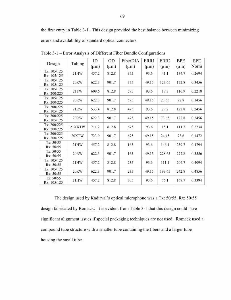
69
the first entry in Table 3-1. This design provided the best balance between minimizing
errors and availability of standard optical connectors.
Table 3-1 – Error Analysis of Different Fiber Bundle Configurations
Design Tubing ID (µm)
OD (µm)
FiberDIA(µm)
ERR1 (µm)
ERR2 (µm)
BPE (µm)
BPE Norm
Tx: 105/125 Rx: 105/125 21HW 457.2 812.8 375 93.6 41.1 134.7 0.2694
Tx: 105/125 Rx: 105/125 20RW 622.3 901.7 375 49.15 123.65 172.8 0.3456
Tx: 105/125 Rx: 200/225 21TW 609.6 812.8 575 93.6 17.3 110.9 0.2218
Tx: 105/125 Rx: 200/225 20RW 622.3 901.7 575 49.15 23.65 72.8 0.1456
Tx: 200/225 Rx: 105/125 21RW 533.4 812.8 475 93.6 29.2 122.8 0.2456
Tx: 200/225 Rx: 105/125 20RW 622.3 901.7 475 49.15 73.65 122.8 0.2456
Tx: 200/225 Rx: 200/225 21XXTW 711.2 812.8 675 93.6 18.1 111.7 0.2234
Tx: 200/225 Rx: 200/225 20XTW 723.9 901.7 675 49.15 24.45 73.6 0.1472
Tx: 50/55 Rx: 50/55 21HW 457.2 812.8 165 93.6 146.1 239.7 0.4794
Tx: 50/55 Rx: 50/55 20RW 622.3 901.7 165 49.15 228.65 277.8 0.5556
Tx: 105/125 Rx: 50/55 21HW 457.2 812.8 235 93.6 111.1 204.7 0.4094
Tx: 105/125 Rx: 50/55 20RW 622.3 901.7 235 49.15 193.65 242.8 0.4856
Tx: 50/55 Rx: 105/125 21HW 457.2 812.8 305 93.6 76.1 169.7 0.3394
The design used by Kadirval’s optical microphone was a Tx: 50/55, Rx: 50/55
design fabricated by Romack. It is evident from Table 3-1 that this design could have
significant alignment issues if special packaging techniques are not used. Romack used a
compound tube structure with a smaller tube containing the fibers and a larger tube
housing the small tube.

70
CHAPTER 4 FABRICATION OF THE OPTICAL MICROPHONE
The fabrication of the optical microphone consists of two parts: (1) the MEMS
optical diaphragm chip, and (2) the fiber bundle. The MEMS chip containing the silicon
nitride diaphragm was fabricated by MEMS Exchange, an umbrella organization that
combines the processing capabilities of many foundries across the country [28]. The
fiber bundle was fabricated at the University of Florida.
4.1. MEMS Exchange Process
The process flow used in the MEMS Exchange process was a modified version of
the process flow designed by Kadirval [8]. Both mask and wafers were purchased
through the MEMS Exchange. The mask was designed at the University of Florida.
Table 4-1 summarizes the wafers used for fabrication of the optical microphone.
Table 4-1 – Wafers Used for Optical Microphone Fabrication [28]
Number of Wafers 5 Material silicon Diameter 100 mm
Surface Finish double side polished Thickness 500 – 525
µm Orientation <100>
Doping Type n-type Quality prime Resistivity 1 – 10 Ω / cm
Initial State virgin Source MX Price per Wafer $ 19.95

71
The process grows the membrane layer out of silicon nitride, and uses a DRIE to
etch the bulk silicon and leave the nitride membrane. Silicon dioxide was used as an etch
stop for the DRIE. The detailed process flow is shown in Appendix A.
Not shown in Appendix A are steps to mount and demount the wafer onto a
handle wafer to provide mechanical support during the DRIE.
4.2. Packaging Process
Different novel packaging strategies for an optical microphone have been
proposed [29,30]. Abeysinghe [29] notes that “adhesives limit the range of operation of
the sensors.” To minimize the amount of adhesives used, the cavity is etched at the end
of the fiber and an anodic bonding process is employed to bond an ultra-thin silicon
wafer to the end of the fiber to serve as a membrane [29]. A diagram of the packaging
technique described in [29] is shown Figure 4-1.
Figure 4-1 – Abeysinghe et al. Packaging Technique.
This packaging technique provides a compact device with a sensor head that is the
diameter of the optical fiber. It would function as a pressure sensor in the configuration
Ultra-thin membrane
Machined cavity
Fiber Core
Fiber Cladding

72
shown above (no vent channel), but modifications could be made to add a vent channel.
With this design, it is difficult to control the mechanical properties of the membrane.
Another possible drawback of the package is the size of the cavity. Depending on the
dimensions of the fiber, the optimal equilibrium membrane position may have both
intensity and interference modulation effect present. If both these effects are present, the
theoretical analysis of the device performance will be very difficult.
A similar packaging technique is proposed by Beggans et al. [30]. Beggans’
technique is more useful for an intensity-modulated device. First, a cavity is machined in
a glass wafer. Then, a hole with a diameter which can accompany an optical fiber is
drilled at the bottom of the cavity through the glass substrate. An ultra-thin silicon wafer
is anodically bonded to the glass substrate, creating a cavity. An optical fiber is inserted
into the cavity through the hole drilled in the substrate and fixed with a bonding agent.
The resulting device is shown in Figure 4-2.
This package allows more flexibility in membrane diameter and equilibrium gap
position, but it does not provide as much control over the equilibrium gap position. As
the fiber is being positioned, an active measurement technique is required to verify
membrane position.
Both techniques presented thus far do not protect the optical fibers. The ideal
package would provide some mechanical support for the optical fibers to reduce the
chances of device breakage. The packaging technique proposed by Kadirval [8] provides
protection for the fibers by using a fiber bundle like the type described in this thesis. The
optical fibers are protected by a steel tube and furcation tubing. Multiple MEMS chips
with through-wafer holes (identical to those used in this thesis) are bonded together in the

73
package. All but one of these chips has the diaphragm removed, and they are used to
make a handle wafer stack. The steel tube containing the fiber bundle is inserted through
the handle wafer stack, and the membrane wafer is placed on the top of the wafer stack.
An illustration of the proposed technique is shown in Figure 4-3.
Figure 4-2 – Beggans et al. Packaging Technique.
This technique provides both a compact package and support for the fibers. A
drawback is the potential angular misalignment (other than normal light incidence)
between the fiber and the membrane. The worst-case angular misalignment depends on
the diameter of the steel tube and the thickness of the handle wafer stack. Increasing the
thickness of the handle wafer stack and decreasing the difference between the diameter of
the fiber and the wafer hole will reduce the worst-case angular misalignment.
Ultra-thin membrane
Machined cavity
Fiber Core
Fiber Cladding
Glass Substrate

74
Figure 4-3 – Kadirval Packaging Technique.
The technique for packaging the optical microphone design proposed in this thesis
is similar to [8]. In this proposed package, a second steel tube is used in place of a handle
wafer stack. This steel tube (package tube) would have an inner diameter equal to the
outer diameter of the steel tube (bundle tube) used in the fiber bundle construction
(approx 830 µm). An illustration of this package is shown in Figure 4-4. Standard
available tubing gauges (Popper & Sons [43]) can provide a flush fit to within tens of
microns for this package configuration. The package tube can be an inch or more long.
Using simple geometry, the worst-case angular misalignment can be calculated.
Assuming a worst case gap of 50 µm between the bundle steel tube and package steel
tube (a reasonable assumption based on available tube gauges), and assuming the
minimum length of 1 in. (25,400 µm) for the package steel tube, the maximum angular
misalignment of the bundle tube in the package tube is 0.113o. If a 2 in. package tube
were used, then the maximum angular misalignment becomes 0.056 o. Therefore, it can
MEMS Diaphragm Chip
Fiber Core
Fiber Cladding
Handle Wafer Stack
Epoxy

75
be concluded that this packaging strategy is capable of virtually eliminating angular
misalignments.
The primary advantages of this package are that it simultaneously provides a
robust package and minimizes the worst case angular misalignment error between the
fiber bundle and the membrane, as demonstrated in the previous paragraph. Also, the
dimensions of the package steel tube can be chosen to either minimize package diameter
or to fit a commercially available calibrator such as the Bruel & Kjaer 4231 Microphone
Calibrator [31]. In addition, the outside of the package steel tube could be threaded to
allow a protective screen to be attached over the membrane, protecting it from damage.
For an example of this type of protective screen, see those used by Bruel & Kjaer
1” [32], ½” [33], and 1/8” [34] microphones. Another advantage of this package is the
ability to take multiple packaged optical microphones and easily assemble them into a
microphone array bundle.

76
Figure 4-4 – Proposed Package for the Optical Microphone.
In the top view in Figure 4-5, seven packaged optical microphones are shown in a
bundle surrounded by an array package steel tube, whose dimensions would be selected
to make the fit as tight as possible. The cylindrical structure of the individual
microphone packages allows the microphone array geometry to be a scaled version of the
fibers in the individual microphone package. This allows an arbitrary number of “rings”
of packaged microphones to be used in the array, without the individual packaged
microphones interfering (mechanically) with each other. In addition, the cylindrical
structure of the proposed array package would be easy to construct, using only a custom
MEMS Diaphragm Chip
Bundle Steel Tube
Package Steel Tube
Epoxy
Epoxy
Device Furcation Tubing
> 1”

77
steel tube and epoxy to hold it together. Due to the steel tubing, this proposed array
package would be very robust.
Figure 4-5 – Proposed Optical Microphone Array Package.
Top View
Side View
1 mm 2.5 mm
7.5 mm
9.5 mm

78
In Figure 4-5, the membranes have been removed from the square chips to show
the individual microphone cavity positions. This proposed microphone array could
sample the acoustic field on the center 50 µm of the 1 mm diameter diaphragm. Each
diaphragm is 2.5 mm from each of its neighbors. Finally, the performance of the
microphones in the array is independent of the number of microphones in the array
(assuming the array package does not affect the sound field and availability of sufficient
light sources, detectors, etc).

79
CHAPTER 5 EXPERIMENTAL SETUP AND RESULTS
The experimental characterization of the optical microphone is divided into three
sections. First is the experimental characterization of the laser and photodetector. This
characterization measures the value of Plaser_noise(Plaser) (compare to Plight_noise in Chapter
2). The experimentally measured value Plaser_noise(Plaser) is used as an input to the
theoretical model of the microphone presented in Chapter 2.
Second is the static calibration of the custom fiber bundle. This static calibration
attempts to verify the theoretical power coupled vs. equilibrium gap and sensitivity vs.
equilibrium gap plots. The static calibration curve measured in this experiment is used to
identify the location of the fiber bundle with respect to the membrane in the dynamic
calibration experiments.
The final experimental step is the dynamic calibration of the optical microphone.
In the dynamic calibration, a plane wave tube (pwt), speaker, and calibrated microphone
are used to determine the optical microphone sensitivity, linearity range, frequency
response, noise floor, dynamic range, and minimum detectible signal. The experimental
results are then compared with the theoretical predictions. The dynamic calibration is
performed for both the unreferenced and referenced output microphone configurations.

80
5.1. Laser and Photodetector Characterization
5.1.1. Experimental Setup for Laser and Photodetector Characterization
In the characterization of the laser (or other light source), the optical spectrum of
the photodetector was measured for laser outputs of 100 µW through 500 µW, in steps of
50 µW. The noise power spectral density of the detector output, in V / Hz½, was
recorded by the Pulse system from 0 – 6.4 kHz with a bin width of 1 Hz and using 500
samples. This value is the RMS sum of the detector noise and detected light intensity
noise, both in V / Hz½. The optical intensity noise component of the detector noise is
determined by removing the theoretical Vdet from the measured value, leaving Vlight (see
Section 2.2.4 for variable definitions). By dividing Vlight by the photodetector
responsivity and gain, the optical intensity noise of the laser, in V / Hz1/2, can be
determined.
Figure 5-1 – Experimental Setup for Laser Characterization.
The DC optical power was obtained by observing the 0 Hz frequency bin. The
worst-case light source noise recorded at 660 Hz, and the best-case noise (where the laser
Acoustical Signal System Component
KEY Electrical Signal
System Output
System Input
Optical Signal
PDA-400 Photodetector
Pulse System
Computer Ethernet Port
HP8168B Laser
ISS-1550 Opto-isolator

81
noise became constant with respect to frequency) was measured at 1600 Hz. The
experimental setup for the laser noise characterization is shown in Figure 5-1.
5.1.2. Results of Laser and Photodetector Characterization
The experimentally measured value for Plaser_noise is given by the last column in
Table 5-1. The HP8168B was observed to have a flat noise floor above 1550 kHz.
Below 1.55 kHz, the noise floor was not flat. Since this system would ideally be used
with a heterodyne detection scheme to operate the microphone in the flat noise range of
the light source, the laser linearity and MDS will be experimentally measured above 1550
Hz. For all laser characterization experiments, Gdet = 15,000 V / A.
Table 5-1 – Experimental HP8168B Noise
Laser Power (µW)
Measured Noise @ 1600 Hz
(uV / Hz1/2)
Calculated Laser Noise @ 1600 Hz
(pV / Hz1/2)
Laser SNR @ 1600 Hz
(dB) 100 0.741 52.0 53.0 150 1.29 90.2 52.4 200 1.53 108 52.9 250 1.06 74.4 55.6 300 1.98 139 53.6 350 0.774 54.3 58.4 400 1.68 118 55.7 450 3.59 252 52.9 500 3.26 229 53.9
The laser was observed to have a maximum SNR at Plaser = 350 µW. Therefore,
this value will be used to characterize the laser.
5.2. Static Calibration
5.2.1. Experimental Setup for Static Calibration
The static calibration of the optical microphone has two goals. The first goal is to
verify the corrected power coupled model presented in Chapter 2. The second goal is to

82
obtain a power coupled curve for the fiber bundle under consideration, so that it may be
used to measure the equilibrium gap of the assembled microphone package. The
procedure for this is described further in the dynamic calibration section.
In the static calibration experiment used by Kadirval [8], the fiber bundle is
placed flush against a metal mirror. To align the fibers normal to the mirror, Kadirval
assumed that the power coupled into the receive fibers was maximum when the fibers
were aligned normal to the mirror. While there may be a range of equilibrium gap
distances that this assumption is valid for, it is not valid in general, and will result in the
proper alignment of the fibers with the mirror. Kadirval used a micropositioner to move
the fiber bundle with respect to the mirror. Due to the way in which the fiber bundle was
mounted, the fibers were able to slip in the mechanical mount as the micropositioner was
moved. Due to these two problems with the previous static calibration experiment in [8],
the gap measurements reported by the micropositioner were significantly larger than their
actual values, resulting in an incorrect calibration curve.
In this thesis, these two issues have been fixed. The mechanical mounts for the
fiber and the mirror were aligned normal to each other by cubic blocks, which have
parallel surfaces. The mirror was mounted on the micropositioner and was moved with
respect to the fiber bundle, whose position was fixed. The zero position of the mirror was
set by slowly moving the mirror with the micropositioner until mechanical contact with
the mirror was observed. After mechanical contact has been made, the fiber holder is
closed, fixing the fiber bundle in place. Note: the mirror used in these experiments was
slightly rusted and had scratches on its surface. The method of zeroing used here can

83
potentially scratch the mirror, so it should not be used with a mirror in good condition.
An electrical contact method could be used instead.
The static calibration setup used for the optical microphone is similar to the setup
used by Kadirval [8] except as noted in the previous paragraph. The experimental setup
for the static calibration is illustrated in Figure 5-2. In Figure 5-2, the custom fiber
bundle is oriented normal to a reflective mirror, which is mounted on a computer-
controlled micropositioner. The computer-controlled micropositioner is automated by a
Labview application to sample the power output of a reference channel and the output of
the fiber bundle. After taking 30 samples, the micropositioner adjusts the mirror position
relative to the fiber bundle and repeats the measurement. This step-and-sample process
continues until cancelled by the user.
The light source used is the LPS-SMF28-1550-FC laser diode operated in
constant current mode by a Keithley 2400 constant current source. Laser light is passed
through a Newport ISS-1550 optical isolator and is split by a 50/50 optical power splitter.
One output of the splitter delivers light into the Tx fiber of the custom fiber bundle. This
light reflects off of the mirror and is collected by the receive fibers, which transport the
light to a PDA-400 detector (TEST). The second splitter output delivers light directly to
another PDA-400 (REF). A Keithley 2000 multimeter controlled by a Labview
application sampled the TEST and REF detector outputs, and sends the data to a
computer where it is recorded in a file along with the micropositioner position. The gain
of the PDA-400 detectors in the static calibration is 15,000 V / A.
After the experiment is complete, the recorded detector outputs are corrected for
the experimentally measured bias errors of each photodetector. Dividing the bias-

84
corrected TEST data by the bias-corrected REF data and plotting it with respect to the
measured gaps produces the experimental power coupled curve. The results of the static
calibration are presented in the next section.
Figure 5-2 – Block Diagram of Static Calibration.
5.2.2. Results of Static Calibration
The output of the static calibration is an experimental plot of optical power
coupled vs. equilibrium gap distance. This plot is shown in Figure 5-3 shows the static
LPS-SMF28-1550-FC Laser Diode
ISS-1550 Opto-isolator
Optical Splitter 1550 nm
PDA-400 Photodetector
(REF)
Transmit Fiber, Custom Bundle
Keithley 2400 Sourcemeter
Aluminum Mirror
Micropositioner
Micropositioner Controller
Computer Serial Port
Receive Fiber, Custom Bundle
PDA-400 Photodetector
(TEST) Computer GPIB Port
KEY Electrical Signal
Optical Signal
Mechanical Signal
System Input
System Output
System Component
Keithley 2000 Multimeter

85
calibration curve for the optical microphone using the custom fiber bundle. The plot also
shows the theoretically predicted curves for an RPE of 0 µm and an RPE of 10 µm. The
maximum power coupled is slightly higher than theoretically predicted, and the location
of the peak power coupled is at a larger gap than predicted.
0%
5%
10%
15%
20%
25%
30%
35%
40%
45%
0 100 200 300 400 500 600 700 800 900 1000
Gap (µm)
Pow
er C
oupl
ed (W
/W)
RPE = 0 um RPE = 10.0 um Experimental Figure 5-3 – Experimental Power Coupled vs. Equilibrium Gap.
The location and magnitude of the max slope of the experimental curve was
determined by fitting a regression line to points in a 30 µm window on the experimental
power coupled curve. The location of the maximum slope of the regression line was
assumed to be the gap at the maximum slope, and the maximum slope of the regression
line was assumed to be the peak slope of the experimental power coupled curve. The
regression line at the peak slope is shown in Figure 5-4.

86
Table 5-2 – Comparison between Theoretical and Experimental Static Calibration
Category Theoretical (RPE = 0 µm)
Theoretical (RPE = 10 µm) Experimental
Peak Power Coupled 21.6 % 17.2 % 22.1 % Gap @ Peak Power (µm) 500 530 600 Power Coupled @ Max Slope 5.2 % 4.2 % 10.9 %
Gap @ Max Slope (µm) 230 260 360 Maximum Slope (µm-1) 1.094 x 10⁻³ 0.784 x 10⁻³ 0.800 x 10⁻³
y = 0.0008x - 0.162R2 = 0.9948
0.0%
5.0%
10.0%
15.0%
20.0%
25.0%
200 240 280 320 360 400 440 480 520 560 600
Gap (um)
Pow
er C
oupl
ed (W
/ W
)
Figure 5-4 – Experimental Maximum Power Coupled Regression Line Slope.
The R2 value of the regression line in Figure 5-4 indicates the MO stage is linear
over the gap region from 350 µm to 380 µm. Since the membrane deflection is much less
than 30 µm, the MO stage is linear when operated at the maximum sensitivity.
In both Figure 5-3 and Figure 5-4, the experimental power coupled curve is much
less smooth than the theoretical curve. At some gap values the power coupled seems to
be discontinuous with the surrounding power coupled points. This is believed to be
caused by two phenomena. The first cause is table vibrations. The optical table on which

87
the experiments were performed was not isolated from the ground by a cushion of
compressed air. This allows acoustic vibrations traveling through the floor of the room to
vibrate the mirror during the measurement. The second cause is the roughness of the
mirror surface. The mirror used in this experiment was observed to have scratches and
rust spots on the mirror surface. Light interacting with the scratches and rust spots can
cause discontinuities in the measured power coupled.
5.3. Dynamic Calibration
5.3.1. Experimental Setup for Dynamic Calibration
The goal of the dynamic calibration is to characterize the sensitivity, minimum
detectable signal, electronics noise, linearity, and frequency response of the unreferenced
and referenced optical microphone configurations, and to compare the experimental
performance of the microphone with the theoretical performance.
In the both unreferenced and referenced output calibration experiments, the cut-on
frequency of the SRS 560 was 30 Hz, the gain of the SRS 560 was 1 V / V, and the trans-
impedance gain of the PDA-400 detector(s) was 15,000 V / A. Data is taken with the
Pulse system from 0 Hz – 6.4 kHz with a 2 Hz bin width. All single tone measurements
were made with a sinusoidal input at 1600 Hz. A uniform window was used to measure
single tone signals, and a Hanning window was used for measuring broadband or noise
signals. In all experimental setups (Figure 5-5 and Figure 5-6), a B&K 4138 1/8”
microphone [34], pre-calibrated with a B&K 4228 pistonphone [35], is used as a
reference microphone. This microphone is mounted next to the optical microphone at the
end of the plane wave tube, and it connected to an input channel of the Pulse system (not
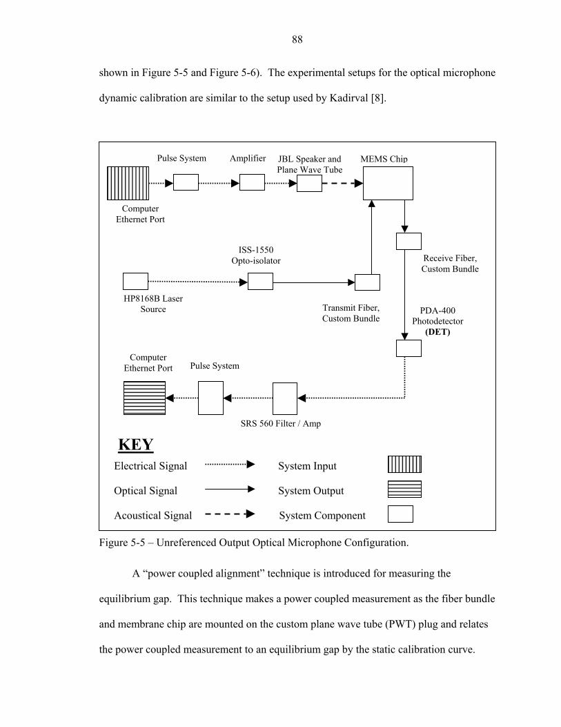
88
shown in Figure 5-5 and Figure 5-6). The experimental setups for the optical microphone
dynamic calibration are similar to the setup used by Kadirval [8].
Fi
eq
an
the
KEY
Transmit Fiber, Custom Bundle
ISS-1550 Opto-isolator
Computer Ethernet Port
Amplifier Pulse System
Pulse System
Computer Ethernet Port
SRS 560 Filter / Amp
PDA-400 Photodetector
(DET)
Receive Fiber, Custom Bundle
JBL Speaker and Plane Wave Tube
Acoustical Signal
gure 5-5 – Unreferenced Output Optic
A “power coupled alignment” te
uilibrium gap. This technique makes
d membrane chip are mounted on the
power coupled measurement to an e
System Component
Electrical Signal
System Output
System Input
HP8168B Laser Source
Optical Signal
al Microphone Co
chnique is introdu
a power coupled m
custom plane wav
quilibrium gap by
MEMS Chip
nfiguration.
ced for measuring the
easurement as the fiber bundle
e tube (PWT) plug and relates
the static calibration curve.

89
The first experimental setup is the unreferenced output configuration, shown in
Figure 5-5. The optical splitter is not required for operation of the microphone in this
configuration. In the unreferenced output configuration, the system output is taken at the
output of the SRS 560 Filter / Amplifier.
Figure 5-6 – Referenced Output Optical Microphone Configura
JBL Speaker and Plane Wave Tube Computer
Ethernet Port
Pulse System
ISS-1550 Opto-isolator
Optical Splitter 1550 nm
TransmCustom
HP8168B Laser Source
PDA-400 Photodetector (REF)
Computer Ethernet
Port
ISS-1550 Opto-isolator
Amplifier
KEY
l
SRS 560 Filter / Amp(Optional)
MEMS Chip
it Fiber, Bundle
PDA-400 Photodetector
(REF)
Receive Fiber, Custom Bundle
Pulse System
10*MOD ---------
REF
Analog Divide CircuitOptical Signal
Acoustical Signa
Electrical Signal
System Output
System Input
System Component
tion.

90
The next setup is the referenced output configuration, shown in Figure 5-6. The
referenced output is also used for the equilibrium gap measurement, since the steady state
output of the analog divide is 10x the power coupled. An estimate of the power coupled
can be made with a voltmeter, but a more accurate value is obtained with the pulse
system.
In order to add optical losses to the reference path (when desired), the reference
isolator was intentionally misaligned with the optical splitter, inducing losses. The
measured optical path losses induced by this intentional misalignment was α = 0.76.
In order to determine the effect of α on the MDS, the losses were removed after
the microphone characterization was completed, and the MDS was measured with α = 0.
5.3.2. Results of the Dynamic Calibration
The microphone output was observed to be slightly unstable for the unreferenced
and referenced microphone, with the referenced microphone the more stable of the two
configurations. The unreferenced configuration instabilities are expected, since the
unreferenced microphone is sensitive to drift in the laser output. These instabilities were
not severe, although it could affect a measurement made by the optical microphone on
rare occasions. Since lasers are inherently unstable, care must be taken to ensure that the
laser is operated at a stable output power, with a minimal amount of power switching
between lasing modes. The most stable output of the laser does not necessarily provide
the maximum intensity SNR, so operating the laser at the optimal SNR point will cause a
stability tradeoff. In general, to minimize the microphone MDS, operate the laser at the
peak intensity SNR. To minimize the effect of instabilities, observe the laser power
stability with an optical spectrometer and operate the microphone at the most stable point.

91
An LED is a more stable light source, and could potentially provide improved
MDS and stability in an optical microphone than a laser source, without requiring optical
isolators. This advantage is countered by the considerably lower coupled power that is
obtained by fiber-coupled LED sources compared to fiber-coupled lasers (as much as
1000 times more power for laser sources). An LED source must provide sufficient output
power for the received optical intensity modulated signal to be detectable by the
photodiode (it is not sufficient for just the steady state received power to be detectable).
Both microphone configurations were observed to be linear up to 122 dB (re. 20
µPa). This linearity is much less than theoretically predicted (160 dB re. 20 µPa). It is
caused by two factors: (1) a significantly lower in-plane stress than the 50 MPa design
goal, and (2) the thickness variation of the membrane measured by the University of
Michigan after the deposition of the nitride (+/- 1 µm). These effects cause the AM
sensitivity to be as much as 15-20 times the design value (see Sec. 2.2.2.1).
y = 0.3165x + 0.2808R2 = 0.9267
0.0
1.0
2.0
3.0
4.0
5.0
6.0
7.0
8.0
9.0
10.0
0 8 15 23 30 38 45 53 60 68 75
Sound Pressure (Pa)
Unr
efer
ence
d M
icro
phon
e O
utpu
t (m
V)
Figure 5-7 – Linearity, Unreferenced Output Configuration.

92
The unreferenced microphone has a problem with linearity. Specifically, the
slope of the linearity curve varies by an unacceptable amount in the microphone linear
region. The unreferenced microphone sensitivity is dependant on the output power of the
light source, which is not stable for a laser. This is because the laser output is known to
drift over time and has small instabilities present at its operating point.
y = 1.7666x + 0.2152R2 = 0.9916
0.0
4.0
8.0
12.0
16.0
20.0
24.0
28.0
32.0
36.0
40.0
0 8 15 23 30 38 45 53 60 68 75
Sound Pressure (Pa)
Unr
efer
ence
d M
icro
phon
e O
utpu
t (m
V)
Figure 5-8 – Linearity, Referenced Microphone Configuration.
From Figure 5-7 and Figure 5-8 the unreferenced and referenced sensitivities can
be observed. The unreferenced output optical microphone has a sensitivity of 0.3165 mV
/ Pa. The referenced output optical microphone has a sensitivity of 1.7666 mV / Pa.
The magnitude response for the unreferenced and referenced microphones was
made with a periodic random noise signal with amplitude equal to 90 dB. For the
unreferenced case, the amplitude of the magnitude response was not equal to the slope of
the linearity regression curve. This is caused by drift and instabilities of the laser output,

93
to which the unreferenced microphone is highly sensitive. The referenced configuration
magnitude response was close to the slope of the referenced microphone linearity curve
regression line.
0
40
80
120
160
200
240
280
320
360
400
0 800 1600 2400 3200 4000 4800 5600 6400
Freq (Hz)
Unr
efer
ence
d M
agni
tude
Res
pons
e ( µ
V/Pa
)
Figure 5-9 – Magnitude Response, Unreferenced Microphone Configuration.

94
0
2
4
6
8
10
12
14
16
18
20
0 800 1600 2400 3200 4000 4800 5600 6400
Freq (Hz)
Ref
eren
ced
Mag
nitu
de R
espo
nse
(mV/
Pa)
Figure 5-10 – Magnitude Response, Referenced Microphone Configuration.
-40-36-32-28-24-20-16-12
-8-4048
1216202428323640
0 800 1600 2400 3200 4000 4800 5600 6400
Freq (Hz)
Unr
efer
ence
d Ph
ase
Res
pons
e (d
egre
es)
Figure 5-11 – Phase Response, Unreferenced Microphone Configuration.

95
-40-36-32-28-24-20-16-12-8-4048
1216202428323640
0 800 1600 2400 3200 4000 4800 5600 6400
Freq (Hz)
Ref
eren
ced
Phas
e R
espo
nse
(deg
rees
)
Figure 5-12 – Phase Response, Referenced Microphone Configuration.
The phase response for both optical microphone configurations is shown in Figure
5-11 and Figure 5-12. The unreferenced microphone exhibits a flatter phase response
than the referenced optical microphone. The referenced optical microphone was
observed to have partial coherence between the optical noise in the modulated and
reference signal paths. This partial coherence, which is not the same at every frequency
bin, is believed to be responsible for the random nature of the referenced phase response.
The measured electrical noise floor of the unreferenced microphone at 1600 Hz is
0.77 µV / Hz½. For the referenced microphone with α = 0.76, the measured electrical
noise floor at 1600 Hz was 5.63 µV. When α = 0, the measured electrical noise floor at
1600 Hz was 5.63 µV. Since increasing alpha was experimentally observed to increase
sensitivity (not shown in plots), the MDS of the referenced optical microphone was

96
improved by adding optical reference path losses. If the optical intensity noise received
by the REF and MOD detectors was highly correlated (more than was observed), then the
optical path losses are expected to increase both the electronic noise and the same factor,
resulting in no improvements to the MDS.
From Figure 5-13 it is observable that the unreferenced noise floor, which is
dominated by laser intensity noise, is not flat. The referenced noise floors are flat in
areas where the unreferenced microphone has noise peaks (the analog divide noise is
negligible). Since both configurations are dominated by the optical intensity noise of the
laser source, the optical intensity noise in the referenced microphone modulated and
reference signal paths must be partially correlated (since only a correlated signal can be
removed by a time-domain division). Since there are frequency ranges where the optical
intensity noise dominates and the referenced noise floor is not flat, the optical noise in the
referenced microphone signal paths is not perfectly coherent at all frequencies.

97
0.01
0.1
1
10
100
1000
10000
0 800 1600 2400 3200 4000 4800 5600 6400
Freq (Hz)
Noi
se F
loor
( µV
/ Hz1/
2 )
Unref Noise Floor
Ref Noise Floor,Alpha = 0Ref Noise Floor,Alpha = 0.76
Figure 5-13 – Electrical Noise Floor, Both Microphone Configurations.
Table 5-3 summarizes the performance metrics of the optical microphone in the
unreferenced output configuration, which used the experimental setup in Figure 5-5.
Table 5-4 summarizes the performance metrics of the optical microphone in the
referenced output configuration, which used the experimental setup in Figure 5-6. The
reported MDS in both tables is taken with a 2 Hz bin width at a center frequency of 1600
Hz.

98
Table 5-3 – Experimental Results of Unreferenced Output Microphone Dynamic Calibration
Laser Power (µW)
PDA 400 Gain
(V / A)
SRS 560 Gain
(V / V)
Sensitivity(mV / Pa)
Frequency Response
(Hz)
MDS (dB re. 20
µPa)
Dynamic Range (dB)
350 15,000 1 0.320 300 – 6400* 65 65 – 122
* The low end of frequency response is set by the lack of a well-defined vent channel. The upper end is limited by the range of the plane wave tube over which only the first propagation mode is supported.
Table 5-4 – Experimental Results of Referenced Output Microphone Dynamic Calibration
Laser Power (µW)
PDA 400 Gain
(V / A)
SRS 560 Gain
(V / V)
Sensitivity(mV / Pa)
Frequency Response
(Hz)
MDS (dB re. 20
µPa)
Dynamic Range (dB)
350 15,000 (both
detectors) 1 1.77 300 –
6400* 47 47 – 122
* The low end of frequency response is set by the lack of a well-defined vent channel. The upper end is limited by the range of the plane wave tube over which only the first propagation mode supported.

99
CHAPTER 6 CONCLUSIONS AND FUTURE WORK
6.1. Conclusions
In conclusion, the MEMS-based intensity-modulated optical microphone is an
excellent choice for applications with harsh environmental or size constraints. Optical
MEMS microphones are currently marketed as a surveillance technology, as an EMI and
RFI immune technology, and as a suitable technology for use in automobile voice
recognition systems (see [36 and 37]).
Intensity-modulated MEMS optical microphones can be configured to provide a
MDS, sensitivity, and electronic noise that is competitive with other microphones of
comparable size. It is also possible to design the optical microphone with a significantly
higher sensitivity and lower MDS by sacrificing frequency response and reducing the
upper limit of the microphone’s dynamic range. It is difficult to make an intensity-
modulated MEMS optical microphone with a high sensitivity, low noise floor, low MDS,
high frequency response, and high upper limit to the dynamic range. This is due to
inherent tradeoffs of the AM stage linearity and frequency response with the AM stage
sensitivity. Alternate, more sensitive, fiber geometries are required to make an intensity-
modulated optical microphone suitable for aero-acoustic measurements.

100
6.2. Future Work
There are many different areas for future research and development of optical
microphones. The coupled equations for sensitivity, electronics noise, and minimum
detectable signal presented in Chapter 2 can be used in a microphone design optimization
problem (see Papila et al. [38]). This would allow a designer to optimize the microphone
performance, given a set of design constraints.
A laser can provide as much as 1000 times more power than an LED source when
used as a light source in an intensity-modulated lever microphone. Laser sources require
opto-isolators to provide output power stability for continuous-wave (CW) operation, and
are generally less stable than LED sources. A future generation version of the optical
microphone could be implemented with a single, large-core, high-NA fiber (instead of a
fiber bundle) using an LED as a light source to improve stability and frequency response.
Since the sensitivity of an unreferenced microphone with LED source is very low
compared to a laser source, novel techniques to couple greater than 50 – 100 µW of
power into the transmit fiber must be used. If the optical power coupled into the transmit
fiber(s) is not sufficiently high, then the microphone MDS will be limited by the MDS of
the photodetectors and other electronics. When lasers are used as light sources, this is not
an issue.
Another area of future work is to implement a robust package for the optical
microphone. A package such as the one presented in Figure 4-4 and Figure 4-5 would be
a good choice for implementation. Since the performance of a MEMS device is
application specific, multiple packages that are tuned to the specific requirements of each

101
optical microphone application should be developed. In addition, an array packaging
technique should be developed to take advantage of the small size of the MEMS device.
The inherent immunity of the MEMS optical microphone to adverse environments
should be further explored. The utility of optical microphones in a high-EMI
environment has been demonstrated by Phone-Or, but the separation of the electronics
and the sensing element allows an optical microphone to potentially be useful in other
harsh environments, such as underwater or in high temperatures. The transition to these
environments brings new issues that must be addressed, such as the high acoustic
impedance of water compared to the microphone package, or the effects of thermal
expansion due to convection in high temperature environments. A non-MEMS optical
microphone for high temperature environments (1000 oF) has been developed by Cuomo
et al. [39 and 40].
Finally, alternate configurations of optical microphone should be explored. The
bundle geometry used by this thesis is not optimal. Additional research needs to be done
to determine the optimal bundle geometry by adding focusing optics, and additional or
new fiber structures. Single fiber designs, such as the one used in [39], have been studied
for non-MEMS optical microphones.

102
APPENDIX A MEMS OPTICAL MICROPHONE DIAPHRAGM PROCESS FLOW
Table A-1 – MEMS Exchange Process Flow for Optical Microphone
Major Step Sub-steps Picture
RCA Clean
HF Dip Dry / Wet /Dry
Oxidization
Oxide Growth
4:1 Sulfuric / Peroxide Bath
HCl Dip
50:1 HF Dip
LPCVD Silicon Nitride Deposition
Nitride deposition
Dehydration Bake
HDMS Prime
Photoresist Coat
Photoresist Coat with Hardbake
Photoresist Hardbake
~ 500 µm Silicon
~ 0.7 µm SiO2
~ 500 µm Silicon
0.7 µm SiO2
1 µm SixNy
~ 500 µm Silicon
0.7 µm SiO2
1 µm SixNy
2.7 µm Photoresist

103
103
Table A-1. Continued
Major Step Sub-steps Picture
Silicon Nitride RIE Reactive Ion Etch
Dehydration Bake
Photoresist Coat
Alignment and Exposure
Contact Photolithography
Develop and Hardbake
Buffered Oxide Etch Oxide Etch
with Buffered HF
~ 500 µm Silicon
0.7 µm SiO2
1 µm SixNy
2.7 µm Photoresist
~ 500 µm Silicon
0.7 µm SiO2
1 µm SixNy
2.7 µm Photoresist
10 µm Photoresist
~ 500 µm Silicon
0.7 µm SiO2
1 µm SixNy
2.7 µm Photoresist
10 µm Photoresist

104
104
Table A-1. Continued
Major Step Sub-steps Picture
Silicon DRIE Silicon Deep Reactive Ion
Etch
Photoresist Ashing Resist ash
Buffered Oxide Etch Oxide Etch
with Buffered HF
Aluminum E-Beam Evaporation
Aluminum E-Beam
~ 500 µm Silicon
0.7 µm SiO2 1 µm SixNy 0.08 µm Al
~ 500 µm Silicon
0.7 µm SiO2
1 µm SixNy
~ 500 µm Silicon
0.7 µm SiO2
1 µm SixNy
~ 500 µm Silicon
0.7 µm SiO2
1 µm SixNy
2.7 µm Photoresist

105
APPENDIX B FIBER BUNDLE PROCESS FLOW
The fiber bundle used for the optical microphone was designed and fabricated at
the University of Florida. The Guide to Connectorizing and Polishing Optical Fibers
published by Thorlabs [41] provided a starting point for the development of the process.
The fabrication of the fiber bundle is done in two steps: bundle assembly and connector
polishing.
Table B-1 – Materials List for Bundle Assembly
Thorlabs Part Number Component Quantity AFS105/125Y Multimode Optical Fiber 105/125/250
T06F13 Mechanical Buffer Stripper 1 MS403-10 Epoxy Syringe 1
F120 Pack of 24 Hr Room Temperature Curing Epoxy 1
FT030 Reinforced 3.0 mm Diameter Furcation Tubing 4’ 6”
- Shears or Razor Blade 1 - Duct Tape 1
21HW 1 ½ “ Length of Steel Tubing 1 NA (compare to CL-200) 100x Fiber Microscope 1
- Silly Putty (or modeling clay) Small piece - Tape Measure 1
30126D1 FC Connector 1 10440A or 10770A SMA Connector 1
- Paper Towels 3-5 - Light Source (flashlight, laser pointer) 1 - Needle-nosed pliers or tweezers 1
106
The detailed process for fiber bundle assembly is described next. The required
components are listed in Table B-1. A clear workspace of at least 4 feet long and 2 feet
wide, with the edge of a table present is required to assemble the bundles.
The first step in assembling the custom fiber bundles is to cut the optical fiber and
furcation tubing to length. The design goal is a bundle that is approximately 3 feet long.
It is desired that each section have the same length, so three 1’ 6” long sections of
furcation tubing are cut. Next, designate one section of furcation tubing as the device
section, one section as Rx, and one section as Tx. Now cut seven 3’ 4” lengths of optical
fiber. Use a sharp razorblade or sharp pair of scissors to avoid crushing the fiber as it is
cut, which can cause cracking.
The second step is to strip the buffer off of the ends of the optical fibers. It is the
most labor intensive part of the custom fiber bundle construction, and requires care not to
damage the unprotected fibers. The design goal is for 3.5” or more of buffer to be
removed from the end of the fibers that will be threaded through the steel tubing, and for
1-1.5” to be removed from opposite end of the fibers, which will be connectorized. To
remove the buffer, place the length of fiber on the table, with the end to be stripped
extending approximately 2 cm off of the table. Fix the fiber to the table with tape or by
applying pressure to it with your hand. It is critical that the fiber be perpendicular to the
table edge and not be able to move during the stripping action, since this will cause the
fiber to break. Insert the fiber into the mechanical buffer stripper (T06F13) as shown in
the Thorlabs guide [41]. The fiber should extend past the cutting blades of the
mechanical stripper by no more than 1-2 mm. Squeeze the cutting blades closed, and pull
the mechanical stripper away from the table to strip the piece of buffer off of the fiber.

107
The pulling motion must be firm and with constant pressure to avoid breaking the optical
fiber. If resistance is encountered as the buffer section is removed, increase the pulling
pressure. If there is a pause after the stripping motion begins, the fiber will break.
Continue to strip the buffer in 1-2 mm long segments, repositioning the fiber as
necessary, until the desired length of buffer has been stripped from the end of the fiber.
If the fiber breaks during stripping, a few options are available. If the break
shortens the fiber length by no more than a 0.5”, it should be possible to continue
stripping the fiber. The end of the fiber to be inserted in the steel tube must be stripped to
the prescribed length. Any length fluctuations in the fiber due to breakage must not
affect the device end of the fibers. If the fiber break shortens the fiber length by greater
than 0.5”, then the fiber will have to be replaced, or all fibers trimmed to the new length.
If the break is more than 1”, re-trimming is not recommended.
After the seven fibers are stripped to the desired length, place them next to each
other, aligned to the buffered/unbuffered (B/U) junction at the device end of the fibers.
Verify all fibers have 3.5” of buffer stripped from the device end of the fibers. Verify the
fibers are all equal in length to within +/- 0.25”. Verify the Tx/Rx ends are all stripped to
roughly 1”. Finally, verify that no cracks are visible in any part of the fibers, since cracks
will prevent the fiber from transmitting light.
After the buffer stripping is completed, the fibers must be threaded through the
device section of the furcation tubing. The easiest method to accomplish this is to
remove the pull-string from the inside of the furcation tubing, tape the tube to the table,
and push the seven fibers through the tube at the same time. The fibers should extend
from the end of the furcation tube by approximately 6”.

108
Figure B-1 – Fiber Placement in the Steel Tube.
The next step is the most difficult step in the entire process. The seven fibers
must be inserted into the steel tubing. They must all be inserted together, and they must
be approximately 1” of stripped fibers extending from the end of the steel tube. No
epoxy is needed yet. For an illustration of this, see Figure B-1. Care must be taken to
gently insert the fibers into the steel tube. Verify all seven fibers have passed through the
tube, and that none have broken. Trim the ends of the stripped fibers so that all are the
same length, as shown in Figure B-1.
The steel tube was selected to be a tight fit for the stripped fibers. Note: the
buffered fibers will not fit. Never push the steel tube closer than 0.25” to the Buffered /
Unbuffered (B/U) boundary, since this will cause the fibers to experience a shear stress
along the B/U boundary. This shear stress will cause some of the fibers to break, and this
breakage may not be noticeable until after the bundle has been completed. This type of
breakage can occur during the drying of the epoxy, so care must be taken to keep the steel
tube away from the B/U boundary at all times.
Device Section Furcation Tubing
(FT030)
Buffered / Unbuffered Fiber Boundary
Steel Tube Cross-Section
1.5” > 0.25” > 1”
Stripped ends trimmed to equal length

109
The next step is identification of the center fiber in the bundle. To identify the
center (Tx) fiber, move the steel tube such that the ends of the fibers are flush with the
end of the steel tube. Ideally, the end of the tube should be near the edge of the table to
allow easy inspection of the fiber ends. If the fibers were not properly trimmed, then it
will be difficult to see the bundle by looking into the end of the tube. Cover the remote
ends of the fibers with a paper towel so that no light can be coupled into them from the
ceiling lights. Isolate one fiber from the covered fiber ends, and use a light source (for
example, a laser pointer) to couple light into the remote end. Look into the steel tube at
the fiber bundle face, and identify the illuminated fiber. If the illuminated fiber is in the
center of the fiber bundle, set the remote end separate from the others. Continue until
every fiber has been inspected. If any fiber does not transmit light, then it is broken and
must be removed. If this happens, the fibers must be removed from the steel tube and the
furcation tubing, and a replacement for the damaged fiber must be cut and stripped.
By now, every fiber has been verified to transmit light, the Tx fiber has been
identified, and the steel tube is properly on the end of the fibers (see Figure B-1). The
next step is to put the remote ends of the optical fibers into their respective furcation tube
sections. The Tx fiber should be pushed into one furcation tube segment, and the six Rx
fibers should be pushed into the third (and last) segment. When the Tx and Rx furcation
tubes are brought into contact with the device furcation tube, the stripped fibers should
extend at least ¾” from the end of the Tx and Rx sections. No buffered fiber should
extend from the furcation tubes by more than a few millimeters.

110
Figure B-2 – Illustration of Furcation Tube Segments after Assembly.
Note that Figure B-2 shows the steel tube placed partially inside the device
furcation tube segment. This is accomplished by pulling the fibers at the Tx and Rx end.
The steel tube should be supported during the pulling process, and guided into the
furcation tube. If the steel tube is pushed into the furcation tubing, it may slide close to
the B/U boundary, and cause the fibers to break.
At this point, the fiber bundle is confirmed to fit together properly. If necessary,
the fibers were trimmed and re-stripped from the Tx/Rx end and/or the Tx/Rx tubes were
resized. The next step is to epoxy the components together. First, arrange the fibers as
shown in Figure B-1. Prepare the epoxy as shown in [41]. Make epoxy beads at the
points shown in Figure B-3. Next, move the steel tube along the fibers to smear the
epoxy inside the tube. Care must be taken to ensure the steel tube does not come closer
that 0.25” to the B/U boundary. Epoxy must cover all parts of the fiber from the end of
1’ 6” 1’ 6” > 1.1” > 0.75”
Tx/Rx Section Furcation Tubing
(FT030)
Device Section Furcation Tubing
(FT030)
Steel Tube
Protruding Fiber Bundle
(7 fibers)
Rx Fiber (6 fibers)
> 0.75”
Tx Fiber (1 fiber)

111
the steel tube to the B/U boundary. When dried, it will provide support for the stripped
fibers whose positions will be fixed and are easily damaged by shear stresses.
Figure B-3 – Epoxy Points for Steel Tube.
Once the epoxy is inside the steel tube, arrange the fibers as shown in Figure B-3
and epoxy the steel tube into the furcation tubing. Fill the open end of the furcation
tubing with epoxy, so that the steel tube is not free to move when the epoxy has dried.
Use the epoxy syringe to place an epoxy bead at the free end of the steel tubing.
To finish the device section of the fiber bundle, the fibers must be forced into a
shape closely approximating the ideal fiber bundle structure shown in Figure 1-10. This
is done by wrapping the optical fibers protruding from the steel tube with a small piece of
silly putty or clay, which must hold its shape during the 24 hr. drying process. The
location of the silly putty wrap is shown in Figure B-4.
Device Section Furcation Tubing
(FT030) Epoxy Points
Move steel tube to smear epoxy

112
Figure B-4 – Location of Epoxy Bead and Putty Wrap.
The silly putty wrap should be squeezed with a small pair of needle-nosed pliers
or tweezers to tighten the ring structure of the bundle. This is critical to the bundle
performance.
The final step of the bundle assembly is to connectorize the Tx and Rx furcation
tubes. For the Tx segment, this process is identical to the connectorization procedure
outlined in [41] using the 30126D1 FC connector. The Rx segment process differs
slightly since multiple fibers are present. Also, the Rx segment requires an SMA
connector. There are two connector models that can be used. The best connector is the
10440A, which has a 440 µm diameter hole. All six Rx fibers will fit in the 10440A if
the cladding has been stripped as described above. A bundle using this connector will be
aligned more accurately with the photodetector. Alternately, if the fibers at the Rx
connector have not all been properly stripped (it is difficult to correct alignment problems
after the steel tube is assembled), then a 10770A SMA connector must be used. This
Device Section Furcation Tubing
(FT030) Epoxy Beads Putty

113
connector has a 770 µm diameter hole, and can hold the six Rx fibers if none have been
properly stripped. Using a 10770A connector makes the polishing process more difficult,
and it makes it difficult to align the Rx fibers with the photodetector. To improve the
alignment of the Rx fibers with the photodetector, use a putty wrap like the kind used for
the steel tube fibers. The assembled connector is illustrated in Figure II-5.
Figure B-5 – Assembled Tx/Rx Connector.
After both connectors have been assembled, the bundle must be maintained until
the epoxy begins to harden (45 minutes). Every five minutes, retighten the putty wraps
and reposition the fibers so that they come out of the center of the steel tube. When the
epoxy begins to harden, wrap the junction of the three furcation tube sections with duct
tape, and allow the epoxy to harden for 24 hours. After the 24-hour period has passed,
the bundle is ready for connector polishing.
The components needed for the polishing of the connector are shown in Table B-
2. The same workspace used to assemble the bundle can be used to polish the
connectors.
Tx/Rx Section Furcation Tubing
(FT030) Epoxy Bead Putty
(Rx only)
Fiber(s) Strain Relief Boot

114
Table B-2 –Materials List for Connector Polishing
Thorlabs Part Number Component Quantity LFG5P Lapping Film, 5 µm Grain 1 LFG3P Lapping Film, 3 µm Grain 1 LFG1P Lapping Film, 1 µm Grain 1 LFG03P Lapping Film, 0.3 µm Grain 1 S90W Diamond Tipped Fiber Scribe 1
N/A (compare to CL-200) 100x Fiber Microscope 1 CTG913 Glass Polishing Plate 1 NRS913 Rubber Polishing Pad 1 D50-FC FC Polishing Disk 1
D50-SMA SMA Polishing Disk 1 - Custom Steel Tube Polishing Disk 1 - Razor Blade 1
KW32 Kim Wipes 1 - Light Source 1
The first step in polishing the fiber bundle connectors is to inspect the bundle and
verify the epoxy is dry. Also, verify the duct tape properly holds the furcation tubing
sections together. Finally, ensure the connectors and putty wraps are not stuck to the
table.
When the bundle is verified to be mechanically stable, polishing may begin. First,
the fibers that protrude from their connectors must be cleaved. The cleaving process is
described in [41], but it must be modified slightly when multiple fibers are present in a
connector. The most fragile connector is the FC connector, since it contains a single Tx
fiber. To cleave the fiber, gently touch the end of the diamond scribe to the Tx fiber at a
location no more than a fiber diameter beyond the epoxy bead (see Figure B-6).

115
Figure B-6 – Location to Cleave Fibers in the Fiber Bundle.
If the fiber is cleaved more than one fiber diameter from the epoxy bead, extra
care must be taken during the initial polishing steps to avoid shattering the end of the
fiber. Next, the fiber bundles protruding from the steel tube and the Rx connector must
be cleaved. Since the bundle of fibers does not cleave with just a touch from the scribe, a
sawing motion may be used with the scribe to cut the fibers. A razorblade may be used if
the fibers do not cleave with the scribe. It is important that the fibers are not broken by
Tx/Rx Section Furcation Tubing
(FT030) Epoxy Bead Putty
(Rx only)
Fiber(s) Cleaving Location
Protrudes < 1 Fiber Diameter

116
bending at the cleave point. This can cause cracks to form in the fibers below the surface
of the connector ferule, adversely affecting performance.
After the fibers have been cleaved, they must be polished. The polishing process
is identical to the process in [41]. In general, the multiple fiber connectors will take
longer to polish, so extra time must be spent with each grain of lapping paper. The
appropriate polishing disk must be used with each connector. Instructions for using the
disks are in [41]. The custom disk for the steel tube is used in the same way as the SMA
and FC disks.
Once the polishing is completed, the bundle must be inspected. The quality of the
polish and the location of the fibers in the fiber bundle should be observed with the fiber
microscope. Also, the fibers should be tested by coupling light into the FC and SMA
connectors, and observing the fiber bundle face in the steel tube. Make a note of fibers
that do not transmit light. Once the inspection of the bundle is complete, the bundle is
ready to use.

117
APPENDIX C MECHANICAL DRAWINGS
Figure C-1 – Custom Plane Wave Tube Mount.
Set Screw
Mounting Screw Holes
Steel Tube Hole
MEMS Chip Recess

118
APPENDIX D PHOTODETECTOR SPECIFICATIONS [42]
Table D-1 – PDA-400 Saturation Power
Detector Saturation Voltage [42] 10 V Photodiode Response [42] 0.95 A/W MaxOptPower*TransGain 10.5 Ω*W
Trans-impedance Gain [42] (V/A)
Maximum Incident Power
(µW) 15,000 701.7 47,000 224.0 150,000 70.1 470,000 22.4
1,500,000 7.01
Table D-2 – PDA-400 Measured Dark Noise
Trans-impedance Gain [42]
(V/A)
Photodiode NEP [42]
(pW / Hz½ )
Photodiode Dark Noise
(V rms @ ∆f = 1 Hz)15,000 8.2 1.17 x 10⁻⁷ 47,000 6.0 2.68 x 10⁻⁷ 150,000 3.8 5.42 x 10⁻⁷ 470,000 3.4 1.52 x 10⁻⁶
1,500,000 2.9 4.13 x 10⁻⁶
Table D-3 – PDA-400 Maximum Received Power at Gain Settings
Trans-impedance Gain [42]
(V/A)
Max Received Power (µW)
15,000 702 47,000 223 150,000 70.2 470,000 22.3
1,500,000 7.02
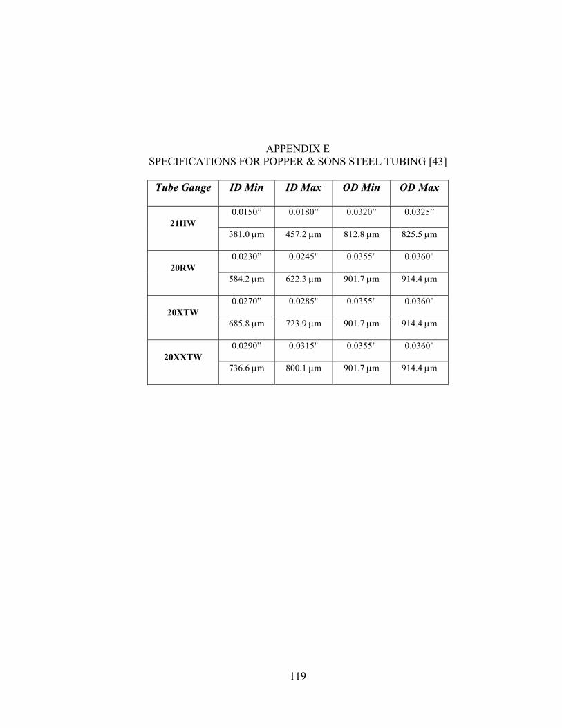
119
APPENDIX E SPECIFICATIONS FOR POPPER & SONS STEEL TUBING [43]
Tube Gauge ID Min ID Max OD Min OD Max
0.0150” 0.0180” 0.0320” 0.0325” 21HW
381.0 µm 457.2 µm 812.8 µm 825.5 µm
0.0230” 0.0245" 0.0355" 0.0360" 20RW
584.2 µm 622.3 µm 901.7 µm 914.4 µm
0.0270” 0.0285" 0.0355" 0.0360" 20XTW
685.8 µm 723.9 µm 901.7 µm 914.4 µm
0.0290” 0.0315" 0.0355" 0.0360" 20XXTW
736.6 µm 800.1 µm 901.7 µm 914.4 µm

120
LIST OF REFERENCES
[1] S. D. Senturia, Microsystems Design. New York: Kluwer Academic, 2001. [2] N. Bilaniuk, "Optical Microphone Transduction Techniques," Applied Acoustics,
vol. 50, pp. 35-63, 1997. [3] V. P. Klimashin, “Optical Microphone,” Pribory i Tekhnika Eksperimenta, no. 3,
pp. 135-137, May 1979. [4] Hu and F. W. Cuomo, “Theoretical and Experimental Study of a Fiber Optic
Microphone,” J. Acoust. Soc. Amer., vol. 91, no. 5, pp. 3049-3056, May 1992. [5] M. H. de Paula and C. A. Vinha, “High-sensitivity Optical Microphone for
Photoacoustics,” American Institute of Physics, Review of Sci. Instrum., vol. 63 no. 6, pp. 3487-3491. June 1992.
[6] W. Lukosz and P. Pliska, “Integrated Optical Nanomechanical Light Modulators
and Microphones,” Sensors and Materials, vol. 3 no. 5, pp. 261-280, 1992. [7] A. Suhadolnik, A. Babnik, and J. Mozina, “Microphone Based on Fiber Optic
Reflective Sensor,” SPIE Proceedings, vol. 2510, pp. 120-127, 1995. [8] K. Kadirval, “Design and Characterization of a MEMS Based Optical Microphone
for Aeroacoustic Measurement,” Master’s Thesis in Electrical and Computer Engineering. Gainesville: University of Florida, 2002.
[9] P. J. Henderson, Rao, Y. J., Jackson, D. A., Zhang, L., and Bennion, I.
“Simultaneous Multi Parameter Monitoring Using a Serial Fiber-Fabry-Perot Array with Low Coherence and Wavelength-Domain Detection,” Meas. Sci. Technol. vol. 9. pp. 1837-1839. 1998.
[10] Norbert Furstenau, Horack, H., and Schmidt, W. “Extrinsic-Fabry-Perot
Interferometer Fiber-Optic Microphone,” IEEE Transactions on Instrumentation and Measurement. vol. 47. no. 1. pp. 138-142. 1998.
[11] Weichong Du, Tao X., and Tam, H. Y. “Temperature Independent Strain
Measurement with a Fiber Grating Tapered Cavity Sensor.” IEEE Photonics Technology Letters. vol. 11. no. 5. pp. 596-598. 1999.

121
[12] D. Greywall, “Micromachined Optical Interference Microphone,” Sensors and
Actuators A Physical, vol. 75, pp. 257-268, 1999. [13] Y. J. Rao, Cooper, M. R., Jackson, D. A., Pannell, C. N., and Reekie, L.
“Simultaneous Measurement of Displacement and Temperature Using In-Fiber-Bragg-Grating-Based Extrinsic Fizeau Sensor.” Electronics Letters. vol. 36. no. 19. pp. 1610-1612. Sept. 14, 2000.
[14] D. C. Abeysinghe, Dasguptam, S., Boyd J.T., Jackson H.E., "A Novel MEMS
Pressure Sensor Fabricated on an Optical Fiber," IEEE Photonics Technology Letters, vol. 13, pp. 993-995, 2001.
[15] A. Wang, Xiao, H., Wang, J., Wang, Z., Zhao, W., May, R.G. “Self-Calibrated
Interferometric-Intensity-Based Optical Fiber Sensors,” J. Lightwave Tech., vol. 19 no. 10, pp. 1495-1501, Oct. 2001.
[16] G. He, Cuomo, F.W, "Displacement Response, Detection Limit, and Dynamic
Range of Fiber-Optic Lever Sensors," Journal of Lightwave Technology, vol. 9, no. 11, pp. 1618-1625, 1991.
[17] M. Sheplak, Seiner, J.M., Bruer K.S, Schmidt M.A, "A MEMS Microphone for
Aeroacoustics Measurements," 37th Aerospace Science Meeting and Exhibit AIAA 99-0606, Reno, NV. Jan 11-14, 1999.
[18] G. He, Cuomo, F.W, "A Light Intensity Function Suitable for Multimode Fiber-
Optic Sensors," Journal of Lightwave Technology, vol. 9, pp. 545-551, 1991. [19] Y. Z. Ruan and L. B. Felson, “Reflection and Transmission of Beams at a Curved
Interface,” J. Optical Society of America A, vol. 3 no. 4, pp. 566-579, April 1986. [20] M. Sheplak and J. Dugundji, “Large Deflections of Clamped Circular Plates Under
Initial Tensions and Transitions to Membrane Behavior,” J. Appl. Mech., vol. 65, pp. 107-115, March 1998.
[21] R. Sahni, “Design of a MEMS-Based Piezoresistive Microphone,” Master's Thesis
in Aerospace and Engineering Mechanics. Gainesville: University of Florida, 2001. [22] G. He, Cuomo, F.W, "The Analysis of Noises in a Fiber Optic Microphone,"
Journal of the Acoustical Society of America, vol. 92, no. 5, pp. 2521-2526, 1992. [23] J. Wilson and J. Hawkes, Optoelectronics, Hemel Hempstead Hertfordshire:
Pretence Hall Europe, 1998.

122
[24] Analog Devices, AD734 Product Data Sheet, Norwood, MA: Analog Devices. [25] L. Coldren and S. Corzine, Diode Lasers and Photonic Integrated Circuits, New
York: John Wiley & Sons, Inc, 1995. [26] H. L. Chau, Wise, K.D., "Noise Due to Brownian Motion in Ultrasensitive Solid
State Pressure Sensors," IEEE Transactions on Electron Devices, vol. ED-34, pp. 859-864, 1987.
[27] S. Horowitz, “A MEMS-Based Single Fiber Optical Lever Microphone,” High
Honors’s Thesis in Electrical and Computer Engineering. Gainesville: University of Florida, 2000.
[28] MEMS Exchange Web Site, www.mems-exchange.org, Reston, Va. June 17, 2003. [29] D. C. Abeysinghe, Dasguptam, S., Boyd J.T., Jackson H.E., "A Novel MEMS
Pressure Sensor Fabricated on an Optical Fiber," IEEE Photonics Technology Letters, vol. 13, pp. 993-995, 2001.
[30] M. H. Beggans, et al. “Optical Pressure Sensor Head Fabrication Using Ultra-Thin
Silicon Wafer Anodic Bonding,” SPIE Symposium on the Design, Test, and Microfabrication of MEMS and MOEMS, Paris, France, vol. 3680, pp. 773-782, March – April 1999.
[31] Bruel & Kjaer, Type 4231 Microphone Calibrator Product Data Sheet, Naerum,
Denmark: Bruel & Kjaer. [32] Bruel & Kjaer, Type 4145 1” Microphone Product Data Sheet, Naerum, Denmark:
Bruel & Kjaer. [33] Bruel & Kjaer, Type 4191 1/2” Microphone Product Data Sheet, Naerum,
Denmark: Bruel & Kjaer. [34] Bruel & Kjaer, Type 4138 1/8” Microphone Product Data Sheet, Naerum,
Denmark: Bruel & Kjaer. [35] Bruel & Kjaer, Type 4231 Microphone Calibrator Product Data Sheet, Naerum,
Denmark: Bruel & Kjaer. [36] Phone-Or, “Optical Microphone for Speech Recognition Applications,” Yehuda,
Israel: Phone-Or. [37] Phone-Or, Surveillance Optical Microphone (SOM) Product Data Sheet, Or-
Yehuda, Israel: Phone-Or.

123
[38] M. Papila, R. Haftka, T. Nishida, and M. Sheplak. “Piezoresistive Microphone Design Paretto Optimization: Tradeoff between Sensitivity and Noise Floor,” 44th Structures, Structural Dynamics, and Materials Conference AAIA 03-0710, July 2003.
[39] F. W. Cuomo, T. D. Nguyen, and A. J. Zuckerwar. “High-Temperature Fiber-Optic
Lever Microphone Incorporating a Single Fiber,” Journal of the Acoustical Society of America, vol. 93, no. 4, p. 2523, 1993.
[40] A. J. Zuckerwar, F. W. Cuomo, T. D. Nguyen, S. A. Rizzi, and S. A. Clevenson.
“High-Temperature Fiber-Optic Lever Microphone,” Journal of the Acoustical Society of America, vol. 97, no. 6, pp. 3605 - 3616, 1995.
[41] Thorlabs, Inc, Guide to Connectorizing and Polishing Optical Fibers, Newton, New
Jersey: Thorlabs, Inc. [42] Thorlabs, Inc, PDA-400 Switchable Gain InGaAs Amplified Photodetector Product
Data Sheet, Newton, New Jersey: Thorlabs, Inc. [43] Popper & Sons, Type 304 Stainless Steel Needle Tubing, Hyde Park, New York:
Popper & Sons.

124
BIOGRAPHICAL SKETCH
Walter Lee Hunt, Jr. was born on July 1, 1977, in Ocala, Florida. He graduated from
high school at Marianna High School in Marianna, Florida, in 1995. Afterwards, he
attended Chipola Junior College in Marianna until graduating in 1997 and transferring to
the University of Florida. In August of 2000, the University of Florida awarded him
Bachelor of Science degrees in computer engineering and in electrical engineering. Since
then, he has worked for the Interdisciplinary Microsystems Group at the University of
Florida as a research assistant while pursuing a Master of Engineering degree,
specializing in electrical engineering. Mr. Hunt’s research interests include the
theoretical study and experimental characterization of optical MEMS sensors, and
MEMS optical microphones in particular.