dca-j agilent 86100c wide-bandwidth oscilloscope mainframe ... 54754a data... · agilent 86100c...
TRANSCRIPT
Agilent 86100CWide-Bandwidth OscilloscopeMainframe and Modules
Technical Specifications
DCA-J
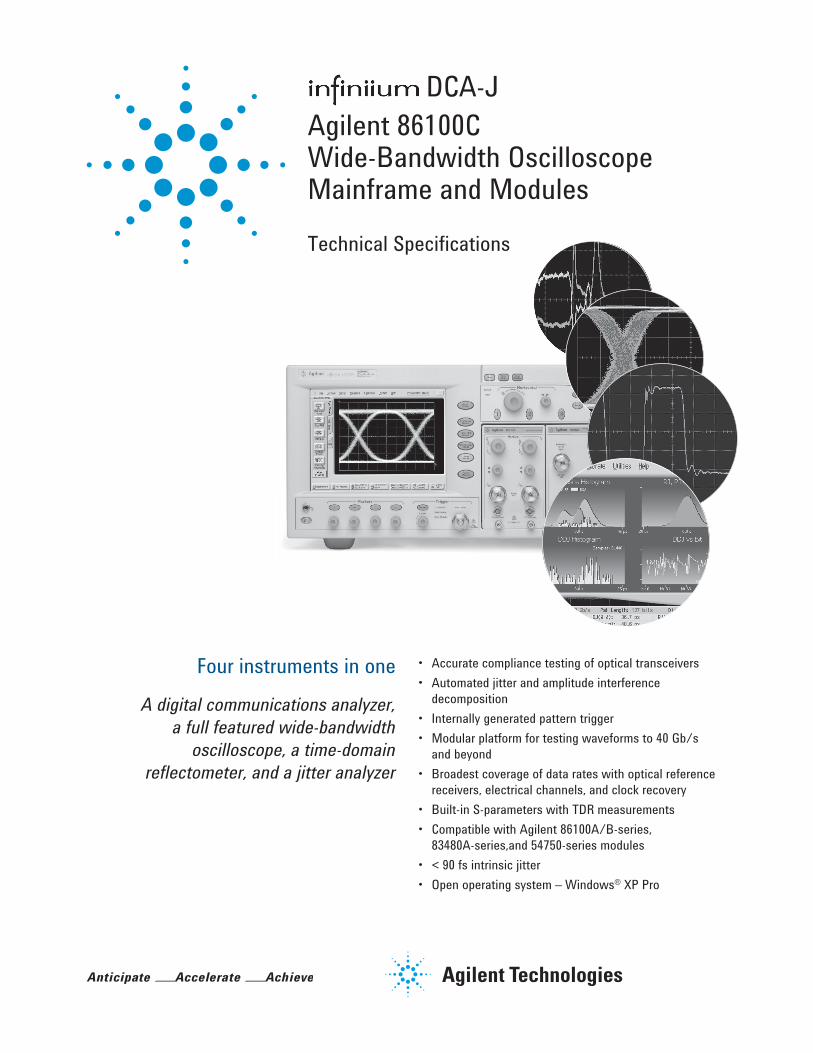
Four instruments in one
A digital communications analyzer,a full featured wide-bandwidth
oscilloscope, a time-domainreflectometer, and a jitter analyzer
• Accurate compliance testing of optical transceivers• Automated jitter and amplitude interference
decomposition• Internally generated pattern trigger• Modular platform for testing waveforms to 40 Gb/s
and beyond• Broadest coverage of data rates with optical reference
receivers, electrical channels, and clock recovery• Built-in S-parameters with TDR measurements• Compatible with Agilent 86100A/B-series,
83480A-series,and 54750-series modules• < 90 fs intrinsic jitter• Open operating system – Windows® XP Pro
2
Overview of Infiniium DCA-J Features ................................................ 3 Eye diagram mask testing ............................................................... 4 Jitter analysis (Option 200) ............................................................. 5 Advanced EYE Analysis (Option 401) ............................................ 5 Equalization and advanced waveform analysis (Option 201) ... 6 Phase noise/jitter spectrum analysis ........................................... 7 PLL bandwidth/jitter transfer ......................................................... 7 S-parameters and time domain reflectometery/time domain transmission (TDR/TDT) ................................................................. 7Measurements ......................................................................................... 8Additional capabilities ............................................................................ 9Specification ........................................................................................... 13 General and Mainframe ................................................................. 13 Precision Time Base Module ........................................................ 15 Computer System and Storage ..................................................... 16Modules Overview ................................................................................. 17Modules Selection Table ...................................................................... 18Modules Specifications ........................................................................ 19Ordering Information ............................................................................. 29Warranty Information (Remove All Doubt) .........................Back coverContact Agilent.........................................................................Back cover
Table of Contents
3
Overview of Infiniium DCA-JFeaturesFour instruments in oneThe 86100C Infiniium DCA-J can be viewed as four high-powered instruments in one:• A general-purpose wide-bandwidth sampling oscilloscope.
PatternLock triggering significantly enhances the usability as a general purpose scope.
• A digital communications analyzer• A time domain reflectometer• A precision jitter and amplitude interference analyzer
Just select the desired instrument mode and start making measurements.
Configurable to meet your needsThe 86100C supports a wide range of modules for testing both optical and electrical signals. Select modules to get the specific bandwidth, filtering, and sensitivity you need.
Digital communications analysisAccurate eye-diagram analysis is essential for characterizing the quality of transmitters used from 100 Mb/s to 40 Gb/s. The 86100C is designed specifically for the complex task of analyz-ing digital communications waveforms. Compliance mask and parametric testing no longer require a complicated sequence of setups and configurations. If you can press a button, you can per-form a complete compliance test. The important measurements you need are right at your fingertips, including:• Industry standard mask testing with built-in margin analysis• Extinction ratio measurements with accuracy and repeatability• Eye measurements: crossing %, eye height and width, ‘1’ and
‘0’ levels, jitter, rise or fall times and more
The key to accurate measurements of lightwave communications waveforms is the optical receiver. The 86100C has a broad range of precision receivers integrated within the instrument.• Built-in photodiodes, with flat frequency responses, yield the
highest waveform fidelity. This provides high accuracy for extinction ratio measurements.
• Standards-based transmitter compliance measurements require filtered responses. The 86100C offers a broad range of filter combinations. Filters can be automatically and repeatably switched in or out of the measurement channel remotely over GPIB or with a front panel button. The frequency response of the entire measurement path is calibrated, and will maintain its performance over long-term usage.
• The integrated optical receiver provides a calibrated optical channel. With the accurate optical receiver built into the module, optical signals are accurately measured and displayed in optical power units.
• Switches or couplers are not required for an average power measurement. Signal routing is simplified and signal strength is maintained.
4
Eye diagram mask testing
The 86100C provides efficient, high-throughput waveform compli-ance testing with a suite of standards based eye-diagram masks. The test process has been streamlined into a minimum number of keystrokes for testing at industry standard data rates.
Standard formatsRate (Mb/s)1X Gigabit Ethernet 12502X Gigabit Ethernet 250010 Gigabit Ethernet 9953.2810 Gigabit Ethernet 10312.510 Gigabit Ethernet FEC 11095.710 Gigabit Ethernet LX4 3125Fibre Channel 1062.52X Fibre Channel 21254X Fibre Channel 42508x Fibre Channel 850010X Fibre Channel 10518.7510X Fibre Channel FEC 1131716x Fibre channel 14025Infiniband 2500STM0/OC1 51.84STM1/OC3 155.52STM4/OC12 622.08STM16/OC48 2488.3STM16/OC48 FEC 2666STM64/OC192 9953.28STM64/OC192 FEC 10664.2STM64/OC192 FEC 10709STM64/OC192 Super FEC 12500STM256/OC768 39813STS1 EYE 51.84STS3 EYE 155.52
Other eye-diagram masks are easily created through scaling those listed above. In addition, mask editing allows for new masks either by editing existing masks, or creating new masks from scratch. A new mask can also be created or modified on an external PC using a text editor such as Notepad, then can be transferred to the instrument’s hard drive using LAN or Flash drive.
Perform these mask conformance tests with convenient user-definable measurement conditions, such as mask margins for guardband testing, number of waveforms tested, and stop/limit actions. Mask margin can be determined automatically to a user definable hit/error ratio. Transmitter waveform dispersion penalty (TWDP) tests can be performed directly in the 86100C. Exporting the waveform for external post processing is not required. (Option 201 and MATLAB® required. Dispersion penalty script for specific test standards must be loaded into the 86100C.)
Eyeline ModeEyeline Mode is available in the 86100C and provides insight into the effects of specific bit transitions within a data pattern. The unique view assists diagnosis of device or system failures due to specific transitions or sets of transitions within a pattern. When combined with mask limit tests, Eyeline Mode can quickly isolate the specific bit that caused a mask violation.
Traditional triggering methods on an equivalent time sampling scope are quite effective at generating eye diagrams. However, these eye diagrams are made up of samples whose timing relationship to the data pattern is effectively random, so a given eye will be made up of samples from many different bits in the pattern taken with no specific timing order. The result is that amplitude versus time trajectories of specific bits in the pattern are not visible. Also, averaging of the eye diagram is not valid, as the randomly related samples will effectively average to the “middle” of the eye.
Eyeline Mode uses PatternLock triggering (Option 001 required) to build up an eye diagram from samples taken sequentially through the data pattern. This maintains a specific timing relationship between samples and allows Eyeline Mode to draw the eye based on specific bit trajectories. Effects of specific bit transitions can be investigated, and averaging can be used with the eye diagram.
PatternLock triggering advances the capabilities of the sampling oscilloscopeThe Enhanced Trigger option (Option 001) on the 86100C provides a fundamental capability never available before in an equivalent time sampling oscilloscope. This new triggering mechanism enables the DCA-J to generate a trigger at the repetition of the input data pattern – a pattern trigger. Historically, this required the pattern source to provide this type of trigger to the scope. With the press of a button, PatternLock automatically detects the pattern length, data rate and clock rate making the complex triggering process transparent to the user.
PatternLock enables the 86100C to behave more like a real-time oscilloscope in terms of user experience. Observation of specific bits within the data pattern is greatly simplified. Users that are familiar with real-time oscilloscopes, but perhaps less so with equivalent time sampling scopes will be able to ramp up quickly.
PatternLock adds another new dimension to pattern triggering by enabling the mainframe software to take samples at specific locations in the data pattern with outstanding timebase accuracy. This capability is a building block for many of the new capabilities available in the 86100C described later.
Overview of Infiniium DCA-JFeatures
5
Jitter analysis (Option 200)
The “J” in DCA-J represents the ability to perform jitter analysis. The 86100C is a Digital Communications Analyzer with jitter analysis capability. The 86100C adds a fourth mode of operation – Jitter Mode. Extremely wide bandwidth, low intrinsic jitter, and advanced analysis algorithms yield the highest accuracy in jitter measurements.
As data rates increase in both electrical and optical applica-tions, jitter is an ever increasing measurement challenge. Decomposition of jitter into its constituent components is becom-ing more critical. It provides critical insight for jitter budgeting and performance optimization in device and system designs. Many communications standards require jitter decomposition for compliance. Traditionally, techniques for separation of jitter have been complex and often difficult to configure, and availability of instruments for separation of jitter becomes limited as data rates increase.
The DCA-J provides simple, one button setup and execution of jitter analysis. Jitter Mode decomposes jitter into its constituent components and presents jitter data in various insightful displays. Jitter Mode operates at all data rates the 86100C supports, removing the traditional data rate limitations from complex jitter analysis. The 86100C provides several key attributes to jitter analysis:• Very low intrinsic jitter (both random and deterministic)
translates to a very low jitter noise floor which provides unmatched jitter measurement sensitivity
• Wide bandwidth measurement channels deliver very low intrinsic data dependent jitter and allow analysis of jitter on all data rates to 40 Gb/s and beyond
• PatternLock triggering technology provides sampling efficiency that makes jitter measurements very fast
• Firmware revision 8.0 allows for accurate jitter measurements on signals with large RJ/PJ components (up to 0.7 UI)
Jitter analysis functionality is available through the Option 200 software package. Option 200 includes:
• Decomposition of jitter into Total Jitter (TJ), Random Jitter (RJ), Deterministic Jitter (DJ), Periodic Jitter (PJ), Data Dependent Jitter (DDJ), Duty Cycle Distortion (DCD), and Jitter induced by Intersymbol Interference (ISI)
• •Variousgraphicalandtabulardisplaysofjitterdata• Export of jitter data to convenient delimited text format• Save / recall of jitter database• Jitter frequency spectrum• Isolation and analysis of Sub-Rate Jitter (SRJ), that is, periodic
jitter that is at an integer sub-rate of the bitrate• Bathtub curve display in both Q and logBER scale• Adjustable total jitter probability
Advanced EYE Analysis (Option 401)
Accurate Jitter Measurements on Long PatternsWhen testing jitter performance against specifications, some standards, such as 10 Gigabit Ethernet, often make use of long patterns such as PRBS31. Longer patterns emulate actual data traffic more accurately and can uncover more problems within a device. However, these long patterns can be a challenge for many instruments that measure jitter and estimate Total Jitter (TJ).
86100CU-401 addresses this challenge by making compliant jitter measurements on long patterns, such as PRBS31 or live traffic. Using powerful jitter analysis algorithms, the software measures RJ, DJ, and calculates estimated TJ, on electrical or optical signals.
Additionally, the application measures high probability jitter such as J2 Jitter, sometimes referred to as “99% Jitter” or “all but 1% of jitter”. It also measures J9 Jitter, defined at a BER of 2.5E-10. Data Dependent Pulse Width Shrinkage (DDPWS), a component of Data Dependent Jitter (DDJ), is also reported when the 86100C DCA-J is equipped with 86100C-200 Enhanced Jitter Analysis.
Compliant Mask Testing using BER ContoursAnother feature of 86100CU-401 is its ability to perform mask testing using specifications BER-contours. This method of mask testing is used when specifications, such as OIF-CEI 2.0 and XFP, define mask test requirements based on a defined bit error ratio for the link. While this type of mask can be modified and tested using conventional mask testing techniques, the 86100C can now perform compliant mask testing using both methods. Sampling scopes, due to their unmatched signal fidelity, are the de facto standard for mask testing.
Flexible Hardware Configuration The software application runs on an external PC, or 86100C DCA-J, running Microsoft Office Excel 2003/2007. It uses any 86100C DCA-J hardware configuration to perform a precision waveform measurement and imports the data into MS Excel for further processing. When performing jitter measurements on high performance devices (RJ < 500 fs), the application is able to leverage 86100C-200 Enhanced Jitter (Jitter Mode), well known for its speed and accuracy. Alternatively, the application can also operate standalone if Jitter Mode is not installed – the choice is yours!
Overview of Infiniium DCA-JFeatures
6
Equalization and advanced waveform analysis (Option 201)
As bit rates increase, channel effects cause significant eye clo-sure. Many new devices and systems are employing equalization and pre/de-emphasis to compensate for channel effects. Option 201 Advanced Waveform Analysis will provide key tools to enable design, test, and modeling of devices and systems that must deal with difficult channel effects:• Capture of long single valued waveforms. PatternLock
triggering and the waveform append capability of Option 201 enable very accurate pulse train data sets up to 256 megasamples long, similar to a very deep memory real-time oscilloscope acquisition.
• Equalization. The DCA-J can take a long single valued waveform and route it through a linear equalizer algorithm (default or user defined) and display the resultant equalized waveform in real time. The user can simultaneously view the input (distorted) and output (equalized) waveforms.
• Interface to MATLAB1 analysis capability. User can define a measurement with a MATLAB script. Result can be reported on oscilloscope results display.
• Automatic dispersion penalty analysis (such as transmitter waveform dispersion penalty or TWDP). User-entered MATLAB scripts used to automatically process waveforms and determine penalty values.
Advanced amplitude analysis/RIN/Q-factor (Option 300)In addition to jitter, signal quality can also be impacted by impair-ments in the amplitude domain. Similar to the many types of jitter that exist, noise, inter-symbol interference, and periodic fluctua-tion can cause eye closure in the amplitude domain. Option 300 can be added to an 86100C mainframe (Option 200 must also be installed) to provide in-depth analysis of the quality of both the zero and one levels of NRZ digital communications signals. Amplitude analysis is performed at a single button press as part of the jitter mode measurement process.• Measurement results are analogous to those provided for jitter
and include Total Interference (TI), Deterministic Interference (dual-Dirac model, DI), Random Noise (RN), Periodic Interference (PI), and Inter-symbol Interference (ISI)
• Tablular and graphical results for both one and zero levels• Export of interference data to delimited text format• Save/recall of interference database• Interference frequency spectrum• Bathtub curve display• Q-factor (isolated from deterministic interference)• Adjustable probability for total interference estimation
Relative Intensity Noise (RIN)Relative Intensity Noise (RIN) describes the effects of laser inten-sity fluctuations on the recovered electrical signal. Like amplitude interference, excessive RIN can close the eye diagram vertically, and therefore affect the power budget or system performance. The DCA-J can measure RIN on square wave as well as industry-standard PRBS and other patterns. In order to avoid having the measurement influenced by inter-symbol interference, the instru-ment searches the pattern for sequences of consecutive bits (for example, five zeroes or five ones) and measures the random noise and the power levels in the center of this sequence. When a reference receiver filter is turned on RIN is normalized to a 1 Hz bandwidth. The user can also choose between RIN based on the one level or on the optical modulation amplitude (RIN OMA according to IEEE 802.3ae). RIN measurements require Options 001, 200, and 300.
1. MATLAB Software is available from Agilent with the purchase of a new DCA-J as Option 061 or Option 062, depending on the Toolboxes you need. MATLAB can also be purchased separately from The MathWorks, Inc. (www.mathworks.com). If users wish to run MATLAB on the 86100C mainframe, they must purchase MATLAB 2008a or an earlier version. Please see www.agilent.com/find/matlab_oscilloscopes for more information.
Overview of Infiniium DCA-JFeatures
7
Phase noise/jitter spectrum analysis
Analysis of jitter in the frequency domain can provide valuable insight into jitter properties and the root causes behind them. The phase locked-loop of the 83496B clock recovery module or 86108A precision waveform analyzer module can effectively be used as a jitter demodulator. Internally monitoring the loop error signal and transforming it into the frequency domain allows the jitter spectrum of a signal to be observed. Through self-calibration, effects of the loop response are removed from the observed signal, allowing accurate jitter spectral analysis over a 300 Hz to 20 MHz span.
This technique provides measurements not available withother test solutions:• Jitter spectrum/phase noise for both clock or data signals• Display in seconds or dBc/Hz• High sensitivity: for input signals > 0.5 Vpp, < –100 dBc/Hz
at 10 kHz offset for 5 Gb/s, –106 dBc/Hz for 2.5 Gb/s, –140 dBc/Hz at 20 MHz offset (integrated spectrum of the instrument jitter from 10 kHz to 20 MHz is less than 100 fs)
• High dynamic range: can lock onto and display signals with > 0.5% pp frequency deviation such as spread spectrum clocks and data
• Data rates from 50 Mb/s to 14.2 Gb/s• Clock rates from 25 MHz to 6.75 GHz
Spectral results can be integrated to provide an estimate of combined jitter over a user-defined span. As both clocks and data signals can be observed, the ratio of data-to-clock jitter can be observed. The displayed jitter spectrum can also be altered through a user-defined transfer function, such as a specific PLL frequency response.
Phase noise analysis is achieved via an external spreadsheet application run on a personal computer communicating to the 83496B/86108A through the 86100C mainframe (typically using a USB-GPIB connection). An 83496A clock recovery module must be upgraded to a “B” version to function in the phase noise system.
PLL bandwidth/jitter transfer
The on-board phase detector of the 83496B and 86108A allows for a precision measurement of phase-locked loop (PLL) band-width, sometimes referred to as jitter transfer. The external soft-ware application discussed above for phase noise/jitter spectrum controls several jitter sources including the Agilent N4903 JBERT, 81150A function generator, N5182A MXG, or pattern generators/sources with delay line or phase modulation inputs (modulated with a 33250A function generator) to provide a modulated stimu-lus to the device under test (DUT). The application will monitor the internal phase detector of the 83496B or 86108A to measure
the stimulus as well as the DUT response. By sweeping the frequency of the jitter stimulus, the ratio of the output jitter to the input jitter provides the PLL bandwidth. The measurement system is extremely flexible and can test input/outputs from 50 Mb/s to 14.2 Gb/s (data signals) and/or 25 MHz to 6.75 GHz (clock signals). Thus several classes of DUTs can be measured including clock extraction circuits, multiplier/dividers, and PLLs. Similar to a phase noise analysis, this capability is achieved via an external application run on a PC.
S-parameters and time domain reflectometery/time domain transmission (TDR/TDT)
High-speed design starts with the physical structure. The transmission and reflection properties of electrical channels and components must be characterized to ensure sufficient signal integrity, so reflections and signal distortions must be kept at a minimum. Use TDR and TDT to optimize microstrip lines, back-planes, PC board traces, SMA edge launchers and coaxial cables.
Analyze return loss, attenuation, crosstalk, and other S-parameters (including magnitude and group delay) with one button push using the 86100C Option 202 Enhanced Impedance and S-parameter software, either in single-ended or mixed-mode signals.
Calibration techniques, unique to the 86100C, provide highest precision by removing cabling and fixturing effects from the measurement results. Translation of TDR data to complete single-ended, differential, and mixed mode S-parameters (including magnitude and group delay) are available through Option 202 and the N1930A Physical Layer Test System software. Higher two-event resolution and ultra high-speed impedance measurements are facilitated through TDR pulse enhancers from Picosecond Pulse Labs1.
HDMI/DisplayPort Automated Cable Compliance TestLeveraging Option 202, the 86100CU-610 and 86100CU-620 HDMI/DisplayPort cable compliance test software allow users to automate HDMI or DisplayPort cable compliance tests using 54754A TDR module on the 86100C DCA-J. The compliance software options offer an intuitive interface with step-by-step diagrammatic guidance yielding accurate results and detailed reports. Pass/fail indicators allow R&D and QA customers to make repeatable compliant measurements without needing detailed knowledge of the specifics of either standard.
N1024B TDR calibration kitThe N1024B TDR calibration kit contains precision standard devices based on SOLT (Short-Open-Load-Through) technology to calibrate the measurement path.
1. Picosecond Pulse Labs 4020 Source Enchancement Module (www.picosecond.com)
Overview of Infiniium DCA-JFeatures

8
Measurements
The following measurements are available from the tool bar, as well as the pull down menus. The available measurements depend on the DCA-J operating mode.
Oscilloscope mode• Time
Rise Time, Fall Time, Jitter RMS, Jitter p-p, Period, Frequency, + Pulse Width, – Pulse Width, Duty Cycle, Delta Time, [Tmax, Tmin, Tedge—remote commands only]
• Amplitude Overshoot, Average Power, V amptd, V p-p, V rms, V top, V base, V max, V min, V avg, OMA (Optical Modulation Amplitude)
Eye/mask mode• NRZ eye measurements
Extinction Ratio, Jitter RMS, Jitter p-p, Average Power, Crossing Percentage, Rise Time, Fall Time, One Level, Zero Level, Eye Height, Eye Width, Signal to Noise, Duty Cycle Distortion, Bit Rate, Eye Amplitude
• RZ eye measurements Extinction Ratio, Jitter RMS, Jitter p-p, Average Power, Rise Time, Fall Time, One Level, Zero Level, Eye Height, Eye Amplitude, Opening Factor, Eye Width, Pulse Width, Signal to Noise, Duty Cycle, Bit Rate, Contrast Ratio
Mask Test• Open Mask, Start Mask Test, Exit Mask Test, Filter, Mask
Test Margins, Mask Margin to a Hit Ratio, Mask Test Scaling, Create NRZ Mask
Advanced measurement options• The 86100C’s software options allow advanced analysis.
Options 200, 201, and 300 require mainframe Option 001. Option 202 does not require Option 86100-001. Option 401 does not require Options 001 and 200 unless a DDPWS measurement is required.
Option 200 enhanced jitter analysis software • Measurements
Total Jitter (TJ), Random Jitter (RJ), Deterministic Jitter (DJ), Periodic Jitter (PJ), Data Dependent Jitter (DDJ), Duty Cycle Distortion (DCD), Intersymbol Interference (ISI), Sub-Rate Jitter (SRJ), Asynchronous periodic jitter frequencies, Subrate jitter components.
• Data displays TJ histogram, RJ/PJ histogram, DDJ histogram, Composite histogram, DDJ versus Bit position, Bathtub curve (log or Q scale)
Option 201 advanced waveform analysis • Measurements
Deep memory pattern waveform, user-defined measurements through MATLAB interface, Transmitter Waveform Dispersion Penalty (TWDP)
• Data displays Equalized waveform
Option 202 enhanced impedence and S-parameters
Option 300 amplitude analysis/RIN/Q-factor (requires Option 200)• Measurements
Total Interference (TI), Deterministic Interference (Dual-Dirac model, DI), Random Noise (RN), Periodic Interference (PI), and Inter-symbol Interference (ISI), RIN (dBm or dB/Hz), Q-factor
• Data Displays TI histogram, RN/PI histogram, ISI histogram
Option 400 PLL and jitter spectrum measurement software• Jitter spectrum/phase noise measurements
Integrated Jitter: Total Jitter (TJ), Random Jitter (RJ), Deterministic Jitter (DJ); DJ Amplitude/Frequency, Jitter Spectrum Graph, Jitter versus Time Graph, Frequency versus Time Graph, JitterHistogram, Post Processed Jitter Measurements, Phase Noise Graph dBc/Hz versus Frequency
• Phase Locked Loop (PLL) measurements PLL Bandwidth, PLL Peaking, Data Rate, Jitter Transfer Function (JTF) Graph, Observed Jitter Transfer (OJTF) Graph, JTF Model.
Option 401 advanced EYE analysis• Jitter measurements
Total Jitter (TJ), Random Jitter (RJ), Deterministic Jitter (DJ), J2 Jitter (J2), J9 Jitter (J9), Data Dependent Pulse Width Shrinkage (DDPWS)* * Requires 86100C-200
• Amplitude measurements Total Interference (TI), Random Noise (RN), Deterministic Interference (DI), Eye Opening
• Mask test Pass/Fail Status, BER limit
TDR/TDT mode (requires TDR module)• Quick TDR, TDR/TDT Setup, Normalize, Response, Rise Time,
Fall Time, Δ Time, Minimum Impedance, Maximum Impedance, Average Impedance, (Single-ended and Mixed-mode S-parameters with Option 202)
9
Additional capabilities
Standard functionsStandard functions are available through pull down menus and soft keys, and some functions are also accessible through the front panel knobs.
Markers• Two vertical and two horizontal (user selectable)
TDR markers• Horizontal — seconds or meter• Vertical — Volts, Ohms or Percent Reflection• Propagation — Dielectric Constant or Velocity
Limit tests• Acquisition limits
◦ Limit Test “Run Until” Conditions — Off, # of Waveforms, # of Samples
◦ Report Action on Completion — Save waveform to memory, save screen image
• Measurement limit test ◦ Specify Number of Failures to Stop Limit Test ◦ When to Fail Selected Measurement — Inside Limits,
Outside Limits, Always Fail, Never Fail ◦ Report Action on Failure — Save waveform to memory,
save screen image, save summary• Mask limit test
◦ Specify Number of Failed Mask Test Samples ◦ Report Action on Failure — Save waveform to memory,
save screen image, save summary
Configure measurements• Thresholds
10%, 50%, 90% or 20%, 50%, 80% or Custom• Eye Boundaries
◦ Define boundaries for eye measurments ◦ Define boundaries for alignment
• Format Units for ◦ Duty Cycle Distortion — Time or Percentage ◦ Extinction/Contrast Ratio — Ratio, Decibel or Percentage ◦ Eye Height — Amplitude or Decibel (dB) ◦ Eye Width — Time or Ratio ◦ Average Power — Watts or Decibels (dBm)
• Top Base Definition Automatic or Custom
• Δ Time Definition ◦ First Edge Number, Edge Direction, Threshold ◦ Second Edge Number, Edge Direction, Threshold
• Jitter Mode ◦ Units (time or unit interval, watts, volts, or unit amplitude) ◦ Signal type (data or clock) ◦ Measure based on edges (all, rising only, falling only) ◦ Graph layout (single, split, quad)
Quick measure configuration• Four user-selectable measurements for Each Mode, Eye-mask,
TDR, etc.• Default Settings (Eye/Mask Mode)
Extinction Ratio, Jitter RMS, Average Power, Crossing Percentage
• Default Settings (Oscilloscope Mode) Rise Time, Fall Time, Period, V amptd
Histograms• Configure
◦ Histogram scale (1 to 8 divisions) ◦ Histogram axis (vertical or horizontal) ◦ Histogram window (adjustable window via marker knobs)
Math measurements• Four user-definable functions Operator — magnify, invert,
subtract, versus, min, max• Source — channel, function, memory, constant, response
(TDR)
CalibrateAll calibrations• Module (amplitude)• Horizontal (time base)• Extinction ratio• Probe• Optical channel
Front panel calibration output level• User selectable –2 V to 2 V
UtilitiesSet time and dateRemote interface• Set GPIB interface
Touch screen configuration/calibration• Calibration• Disable/enable touch screen
Upgrade software• Upgrade mainframe• Upgrade module
10
Additional capabilities
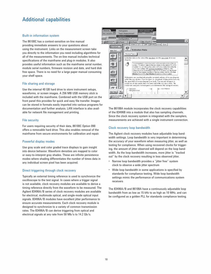
Built-in information systemThe 86100C has a context-sensitive on-line manual providing immediate answers to your questions about using the instrument. Links on the measurement screen take you directly to the information you need including algorithms for all of the measurements. The on-line manual includes technical specifications of the mainframe and plug-in modules. It also provides useful information such as the mainframe serial number, module serial numbers, firmware revision and date, and hard disk free space. There is no need for a large paper manual consuming your shelf space.
File sharing and storageUse the internal 40 GB hard drive to store instrument setups, waveforms, or screen images. A 256 MB USB memory stick is included with the mainframe. Combined with the USB port on the front panel this provides for quick and easy file transfer. Images can be stored in formats easily imported into various programs for documentation and further analysis. LAN interface is also avail-able for network file management and printing.
File securityFor users requiring security of their data, 86100C Option 090 offers a removable hard drive. This also enables removal of the mainframe from secure environments for calibration and repair.
Powerful display modesUse gray scale and color graded trace displays to gain insight into device behavior. Waveform densities are mapped to color or easy-to-interpret gray shades. These are infinite persistence modes where shading differentiates the number of times data in any individual screen pixel has been acquired.
Direct triggering through clock recoveryTypically an external timing reference is used to synchronize the oscilloscope to the test signal. In cases where a trigger signal is not available, clock recovery modules are available to derive a timing reference directly from the waveform to be measured. The Agilent 83496A/B series of clock recovery modules are available for electrical, multimode optical, and single-mode optical input signals. 83496A/B modules have excellent jitter performance to ensure accurate measurements. Each clock recovery module is designed to synchronize to a variety of common transmission rates. The 83496A/B can derive triggering from optical and electrical signals at any rate from 50 Mb/s to 14.2 Gb/s.
The 86108A module incorporates the clock recovery capabilities of the 83496B into a module that also has sampling channels. Since the clock recovery system is integrated with the samplers, measurements are achieved with a single instrument connection.
Clock recovery loop bandwidthThe Agilent clock recovery modules have adjustable loop band-width settings. Loop bandwidth is very important in determining the accuracy of your waveform when measuring jitter, as well as testing for compliance. When using recovered clocks for trigger-ing, the amount of jitter observed will depend on the loop band-width. As the loop bandwidth increases, more jitter is “tracked out” by the clock recovery resulting in less observed jitter.• Narrow loop bandwidth provides a “jitter free” system
clock to observe a wide jitter spectrum• Wide loop bandwidth in some applications is specified by
standards for compliance testing. Wide loop bandwidth settings mimic the performance of communications system receivers
The 83496A/B and 86108A have a continuously adjustable loop bandwidth from as low as 15 kHz to as high as 10 MHz, and can be configured as a golden PLL for standards compliance testing.
11
Additional capabilities
Waveform autoscalingAutoscaling provides quick horizontal and vertical scaling of both pulse and eye-diagram (RZ and NRZ) waveforms.
Gated triggeringTrigger gating port allows easy external control of data acquisi-tion for circulating loop or burst-data experiments. Use TTL-compatible signals to control when the instrument does and does not acquire data.
Easier calibrationsCalibrating your instrument has been simplified by placing all the performance level indicators and calibration procedures in a single high-level location. This provides greater confidence in the measurements made and saves time in maintaining equipment.
Stimulus response testing using the Agilent N490X BERTsError performance analysis represents an essential part of digital transmission test. The Agilent 86100C and N490X BERT have similar user interfaces and together create a powerful test solu-tion. If stimulus only is needed, the 81133A and 81134A pattern generators work seamlessly with the 86100C.
Transitioning from the Agilent 83480A and 86100A/B to the 86100CWhile the 86100C has powerful new functionality that its predecessors don’t have, it has been designed to maintain compatibility with the Agilent 86100A, 86100B and Agilent 83480A digital communications analyzers and Agilent 54750A wide-bandwidth oscilloscope. All modules used in the Agilent 86100A/B, 83480A and 54750A can also be used in the 86100C. The remote programming command set for the 86100C has been designed so that code written for the 86100A or 86100B will work directly. Some code modifications are required when transitioning from the 83480A and 54750A, but the command set is designed to minimize the level of effort required.
IVI-COM capabilityInterchangeable Virtual Instruments (IVI) is a group of new instrument device software specifications created by the IVI Foundation to simplify interchangeability, increase application performance, and reduce the cost of test program development and maintenance through design code reuse. The 86100C IVI-COM drivers are available for download from the Agilent website.
VXII.2 and VXII.3 instrument controlFirmware revision 8.0 provides LAN based instrument control
12
Additional capabilities
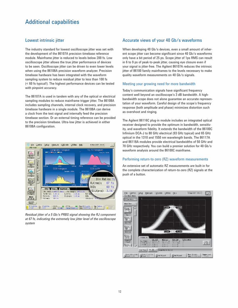
Lowest intrinsic jitter
The industry standard for lowest oscilloscope jitter was set with the development of the 86107A precision timebase reference module. Mainframe jitter is reduced to levels below 200 fs. Low oscilloscope jitter allows the true jitter performance of devices to be seen. Oscilloscope jitter can be driven to even lower levels when using the 86108A precision waveform analyzer. Precision timebase hardware has been integrated with the waveform sampling system to reduce residual jitter to less than 100 fs (< 60 fs typical!). The highest performance devices can be tested with pinpoint accuracy.
The 86107A is used in tandem with any of the optical or electrical sampling modules to reduce mainframe trigger jitter. The 86108A includes sampling channels, internal clock recovery, and precision timebase hardware in a single module. The 86108A can derive a clock from the test signal and internally feed the precision timebase section. Or an external timing reference can be provided to the precision timebase. Ultra-low jitter is achieved in either 86108A configuration.
Accurate views of your 40 Gb/s waveforms
When developing 40 Gb/s devices, even a small amount of inher-ent scope jitter can become significant since 40 Gb/s waveforms only have a bit period of 25 ps. Scope jitter of 1ps RMS can result in 6 to 9 ps of peak-to-peak jitter, causing eye closure even if your signal is jitter-free. The Agilent 86107A reduces the intrinsic jitter of 86100 family mainframes to the levels necessary to make quality waveform measurements on 40 Gb/s signals.
Meeting your growing need for more bandwidthToday’s communication signals have significant frequency content well beyond an oscilloscope’s 3 dB bandwidth. A high-bandwidth scope does not alone guarantee an accurate represen-tation of your waveform. Careful design of the scope’s frequency response (both amplitude and phase) minimizes distortion such as overshoot and ringing.
The Agilent 86116C plug-in module includes an integrated optical receiver designed to provide the optimum in bandwidth, sensitiv-ity, and waveform fidelity. It extends the bandwidth of the 86100C Infiniium DCA-J to 80 GHz electrical (93 GHz typical) and 65 GHz optical in the 1310 and 1550 nm wavelength bands. The 86117A and 86118A modules provide electrical bandwidths of 50 GHz and 70 GHz respectively. You can build a premier solution for 40 Gb/s waveform analysis around the 86100C mainframe.
Performing return-to-zero (RZ) waveform measurementsAn extensive set of automatic RZ measurements are built-in for the complete characterization of return-to-zero (RZ) signals at the push of a button.
Residual jitter of a 5 Gb/s PRBS signal showing the RJ component at 67 fs, indicating the extremely low jitter level of the oscilloscope system
13
SpecificationsGeneral and MainframeSpecifications describe warranted performance over the temperature range of +10 °C to +40 °C (unless otherwise noted). The specifications are applicable for the temperature after the instrument is turned on for one (1) hour, and while self-calibration is valid. Many performance parameters are enhanced through frequent, simple user calibrations. Characteristics provide useful, non-warranted information about the functions and performance of the instrument. Characteristics are printed in italic typeface. Product specifications and descriptions in this document subject to change without notice.
Factory Calibration Cycle - For optimum performance, the instrument should have a complete verification of specifications once every twelve (12) months.
General specificationsTemperatureOperating Non-operating
10 °C to +40 °C (50 °F to +104 °F)–40 °C to +65 °C (–40 °F to +158 °F)
AltitudeOperating Up to 4,600 meters (15,000 feet)Power115 V, 5.7 A, 230 V, 3.0 A, 50/60 HzWeightMainframe without modules Typical module
15.5 kg (34 lb)1.2 kg (2.6 lb)
Mainframe dimensions (excluding handle)Without front connectors and rear feet With front connectors and rear feet
215 mm H x 425 mm W x 566 mm D (8.47 inch x 16.75 inch x 22.2 inch)215 mm H x 425 mm W x 629 mm D (8.47 inch x 16.75 inch x 24.8 inch)
Mainframe specificationsHorizontal system (time base) Pattern lockScale factor (full scale is ten divisions) Minimum Maximum
2 ps/div (with 86107A: 500 fs/div)1 s/div 250 ns/div
Delay1
Minimum Maximum
24 ns1000 screen diameters or 10 s, whichever is smaller
40.1 ns default, 24 ns min1000 screen diameters or 25.401 μs, whichever is smaller
Time interval accuracy2 1 ps + 1.0% of Δ time reading3 or 8 ps, whichever is smaller
Time interval accuracy – jitter mode operation4 1 psTime interval resolution ≤ (screen diameter)/(record length) or
62.5 fs, whichever is largerDisplay units Bits or time (TDR mode–meters)Vertical system (channels)Number of channels 4 (simultaneous acquisition)Vertical resolution 14 bit A/D converter (up to 15 bits with averaging)Full resolution channel Adjusts in a 1-2-5-10 sequence for coarse adjustment or fine adjustment resolution
from the front panel knobAdjustments Scale, offset, activate filter, sampler bandwidth, attenuation factor, transducer
conversion factorsRecord length 16 to 16384 samples – increments of 1
1. Time offset relative to the front panel trigger input on the instrument mainframe.2. Dual marker measurement performed at a temperature within ±5 °C of horizontal calibration temperature.3. The maximum delay setting is 100 ns and delta time does not span across (28 + Nx4)ns ± 100 ps delay setting, where N=0,1,2….18. If delta time measurement span
exceeds above criteria, time interval accuracy is 8 ps +0.1% of ∆ time reading.4. Characteristic performance. Test configuration: PRBS of length 27 – 1 bits, Data and Clock 10 Gb/s.
14
SpecificationsGeneral and Mainframe
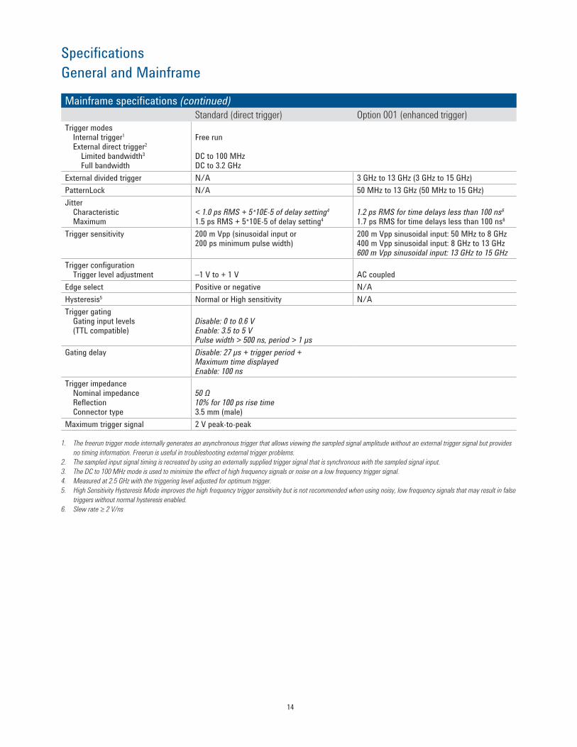
Mainframe specifications (continued)Standard (direct trigger) Option 001 (enhanced trigger)
Trigger modes Internal trigger1 External direct trigger2
Limited bandwidth3 Full bandwidth
Free run
DC to 100 MHzDC to 3.2 GHz
External divided trigger N/A 3 GHz to 13 GHz (3 GHz to 15 GHz)PatternLock N/A 50 MHz to 13 GHz (50 MHz to 15 GHz)Jitter Characteristic Maximum
< 1.0 ps RMS + 5*10E-5 of delay setting4
1.5 ps RMS + 5*10E-5 of delay setting41.2 ps RMS for time delays less than 100 ns6
1.7 ps RMS for time delays less than 100 ns6
Trigger sensitivity 200 m Vpp (sinusoidal input or200 ps minimum pulse width)
200 m Vpp sinusoidal input: 50 MHz to 8 GHz400 m Vpp sinusoidal input: 8 GHz to 13 GHz600 m Vpp sinusoidal input: 13 GHz to 15 GHz
Trigger configuration Trigger level adjustment –1 V to + 1 V AC coupledEdge select Positive or negative N/AHysteresis5 Normal or High sensitivity N/ATrigger gating Gating input levels (TTL compatible)
Disable: 0 to 0.6 VEnable: 3.5 to 5 VPulse width > 500 ns, period > 1 μs
Gating delay Disable: 27 μs + trigger period +Maximum time displayedEnable: 100 ns
Trigger impedance Nominal impedance Reflection Connector type
50 Ω10% for 100 ps rise time3.5 mm (male)
Maximum trigger signal 2 V peak-to-peak
1. The freerun trigger mode internally generates an asynchronous trigger that allows viewing the sampled signal amplitude without an external trigger signal but provides no timing information. Freerun is useful in troubleshooting external trigger problems.
2. The sampled input signal timing is recreated by using an externally supplied trigger signal that is synchronous with the sampled signal input.3. The DC to 100 MHz mode is used to minimize the effect of high frequency signals or noise on a low frequency trigger signal.4. Measured at 2.5 GHz with the triggering level adjusted for optimum trigger.5. High Sensitivity Hysteresis Mode improves the high frequency trigger sensitivity but is not recommended when using noisy, low frequency signals that may result in false
triggers without normal hysteresis enabled.6. Slew rate ≥ 2 V/ns
15
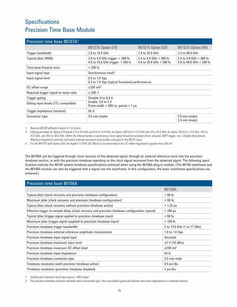
SpecificationsPrecision Time Base Module
Precision time base 86107A1
86107A Option 010 86107A Option 020 86107A Option 040Trigger bandwidth 2.0 to 15.0 GHz 2.4 to 25.0 GHz 2.4 to 48.0 GHzTypical jitter (RMS) 2.0 to 4.0 GHz trigger: < 280 fs
4.0 to 15.0 GHz trigger: < 200 fs2.4 to 4.0 GHz < 280 fs4.0 to 25.0 GHz < 200 fs
2.4 to 4.0 GHz < 280 fs4.0 to 48.0 GHz < 200 fs
Time base linearity error < 200 fsInput signal type Synchronous clock2
Input signal level 0.5 to 1.0 Vpp0.2 to 1.5 Vpp (typical functional performance)
DC offset range ±200 mV3
Required trigger signal-to-noise ratio ≥ 200: 1Trigger gating Disable: 0 to 0.6 V
Enable: 3.5 to 5 VPulse width > 500 ns, period > 1 μs
Gating input levels (TTL compatible)
Trigger impedance (nominal) 50 ΩConnector type 3.5 mm (male) 3.5 mm (male)
2.4 mm (male)
1. Requires 86100 software revision 4.1 or above.2. Filtering provided for Option 010 bands 2.4 to 4.0 GHz and 9.0 to 12.6 GHz, for Option 020 9.0 to 12.6 GHz and 18 to 25.0 GHz, for Option 40 9.0 to 12.6 GHz, 18.0 to
25.0 GHz, and 39.0 to 48.0 GHz. Within the filtered bands, a synchronous clock signal should be provided (clock, sinusoid, BERT trigger, etc.). Outside these bands, filtering is required to minimize harmonics and sub harmonics and provide a sinusoid to the 86107 input.
3. For the 86107A with Option 020, the Agilent 11742A (DC Block) is recommended if the DC offset magnitude is greater than 200 mV.
The 86108A can be triggered through clock recovery of the observed signal, through an external reference clock into the precision timebase section, or with the precision timebase operating on the clock signal recovered from the observed signal. The following speci-fications indicate the 86100 system timebase specifications achieved when using the 86108A plug-in module. (The 86100 mainframe and the 86108A module can also be triggered with a signal into the mainframe. In this configuration, the basic mainframe specifications are achieved.)
Precision time base 86108A86108A
Typical jitter (clock recovery and precision timebase configuration) < 60 fsMaximum jitter (clock recovery and precision timebase configuration)1 < 90 fs Typical jitter (clock recovery without precision timebase active) < 1.25 psEffective trigger-to-sample delay (clock recovery and precision timebase configuration, typical) < 200 psTypical jitter (trigger signal applied to precision timebase input) < 60 fsMaximum jitter (trigger signal supplied to precision timebase input)1 < 100 fsPrecision timebase trigger bandwidth 2 to 13.5 GHz (1 to 17 GHz)Precision timebase external reference amplitude characteristic 1.0 to 1.6 VppPrecision timebase input signal type2 SinusoidPrecision timebase maximum input level ±2 V (16 dBm)Precision timebase maximum DC offset level ±200 mVPrecision timebase input impedance 50 ΩPrecision timebase connector type 3.5 mm maleTimebase resolution (with precision timebase active) 0.5 ps/divTimebase resolution (precision timebase disabled) 2 ps/div
1. Verified with maximum level input signal (~800 mVpp)2. The precision timebase performs optimally with a sinusoidal input. Non-sinusoidal signals will operate with some degradation in timebase linearity.
16
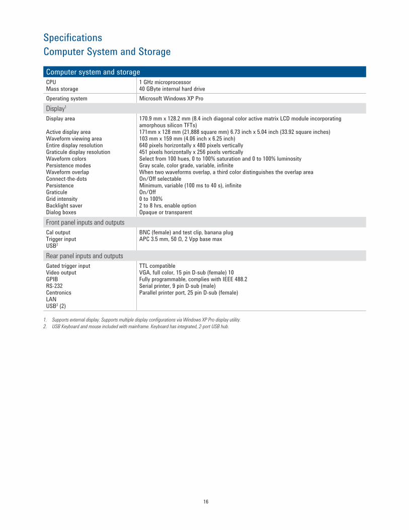
SpecificationsComputer System and Storage
Computer system and storageCPU Mass storage
1 GHz microprocessor40 GByte internal hard drive
Operating system Microsoft Windows XP ProDisplay1
Display area
Active display areaWaveform viewing areaEntire display resolutionGraticule display resolutionWaveform colors Persistence modes Waveform overlap Connect-the-dotsPersistenceGraticule Grid intensityBacklight saverDialog boxes
170.9 mm x 128.2 mm (8.4 inch diagonal color active matrix LCD module incorporating amorphous silicon TFTs)171mm x 128 mm (21,888 square mm) 6.73 inch x 5.04 inch (33.92 square inches)103 mm x 159 mm (4.06 inch x 6.25 inch)640 pixels horizontally x 480 pixels vertically451 pixels horizontally x 256 pixels verticallySelect from 100 hues, 0 to 100% saturation and 0 to 100% luminosityGray scale, color grade, variable, infiniteWhen two waveforms overlap, a third color distinguishes the overlap areaOn/Off selectableMinimum, variable (100 ms to 40 s), infiniteOn/Off0 to 100%2 to 8 hrs, enable optionOpaque or transparent
Front panel inputs and outputsCal outputTrigger inputUSB2
BNC (female) and test clip, banana plugAPC 3.5 mm, 50 Ω, 2 Vpp base max
Rear panel inputs and outputsGated trigger inputVideo outputGPIBRS-232CentronicsLANUSB2 (2)
TTL compatibleVGA, full color, 15 pin D-sub (female) 10Fully programmable, complies with IEEE 488.2Serial printer, 9 pin D-sub (male)Parallel printer port, 25 pin D-sub (female)
1. Supports external display. Supports multiple display configurations via Windows XP Pro display utility.2. USB Keyboard and mouse included with mainframe. Keyboard has integrated, 2-port USB hub.
17
Modules Overview
Optical/electrical modules
750-1650 nmThe 86105C has the widest coverage of data rates with optical modulation bandwidth of 9 GHz and electrical bandwidth of 20 GHz. The outstanding sensitivity (to –21 dBm) makes the 86105C ideal for a wide range of design and manufacturing applications. Available filters cover all common data rates from 155 Mb/s ;through 11.3 Gb/s.
The 86105D is the premier solution for optical waveform analysis for high-speed signals using short or long wavelength technologies. The optical receiver bandwidth exceeds 20 GHz and the electrical bandwidth exceeds 35 GHz, providing excellent waveform fidelity. Switchable compliance filters are available at all common rates from 8.5 to 14.025 Gb/s (16XFC). Sensitivity to –12 dBm.
For high volume manufacturing or testing of parallel optical systems, the 86115D can be used. The 86115D can be configured with two or four optical ports in a single plug-in module. Each port has specifications similar to the optical channel of the 86105D. (The 86115D does not have an electrical channel.) A multiple optical channel plug-in can offer significant savings compared to other configurations.
1000–1600 nm40 GHz and greater optical and electrical channels:The 86116C is the widest bandwidth optical module with more than 65 GHz optical modulation bandwidth (1300 to 1620 nm) and more than 80 GHz electrical bandwidth. Optical reference receiv-ers for 25 or 40 Gb/s rates are available.
Dual electrical modules
86112A has two low-noise electrical channels with > 20 GHz of bandwidth.
86117A has two electrical channels with up to 50 GHz of band-width ideal for testing signals up to 20 Gb/s.
86118A has two electrical channels, each housed in a compact remote sampling head, attached to the module with separate light weight cables. With over 70 GHz of bandwidth, this module is intended for very high bit rate applications where signal fidelity is crucial.
The 86108A has two electrical channels with over 32 GHz (typi-cally 35 GHz) of bandwidth. Clock recovery (similar to the 83496B) and a precision timebase (similar to the 86107A) are integrated into the module to provide the highest precision electrical wave-form measurements. Residual jitter can be < 60 fs and trigger to sample delay is effectively < 200 ps.
Clock recovery modules
Unlike real-time oscilloscopes, equivalent time sampling oscil-loscopes like the 86100 require a timing reference or trigger that is separate from the signal being observed. This is often achieved with a clock signal that is synchronous to the signal under test. Another approach is to derive a clock from the test signal with a clock recovery module.
The 83496A and B provide the highest performance/flexibility as they are capable of operation at any data rate from 50 Mb/s to 13.5 Gb/s, (14.2 Gb/s for 83496B1) on single-ended anddif-ferential electrical signals, single-mode (1250 to 1620nm) and multimode (780 to 1330 nm) optical signals,with extremely low residual jitter. PLL loop bandwidthis adjustable to provide optimal jitter filtering accordingto industry test standards.
The 83496B has higher gain than the 83496A, allowing it to track most spread-spectrum signals. The 86108A module has internal clock recovery similar to the 83496B.
Time domain reflectometry (TDR)
The Infiniium DCA-J may also be used as a high accuracy TDR, using the 54754A differential TDR module.
TDR/TDT analyses are commonly performed by signal-integrity (SI) engineers during the design and validation of high-speed serial links and components. TDR/TDT measurements are also invaluable for maintaining consistent quality in printed circuit board (PCB) and passive-component manufacturing.
The Agilent N1021B TDR 18 GHz differential TDR probe kit con-nects printed circuit boards and other devices without connectors to the 54754A differential TDR/TDT module in the 86100C Infiniium DCA-J wideband oscilloscope mainframe. In conjunction with these hardware components, engineers can use the optional 86100C-202 enhanced impedance and S-parameter software to accurately characterize differential impedances in the time- and frequency domains (for example, reflections and impedances versus time or distance, or magnitude/phase/group delay of S-parameters like SDD11/SDD21).
1. Requires 86100C firmware revision 8.1
18
Modules Selection Table
86100 family plug-in module matrix
The 86100 has a large family of plug-in modules designed for a broad range of data rates for optical and electrical waveforms. The 86100 can hold up to 2 modules for a total of 4 measurement channels.
Filtered data rates
86105C 1002 1 1 750-1650 8.5 20 62.5 -20 ● ● ● ● ● ● ● ● ● ● ● ●200 1 1 750-1650 8.5 20 62.5 -16 ● ● ● ● ● ● ●3002 1 1 750-1650 8.5 20 62.5 -16 ● ● ● ● ● ● ● ● ● ● ● ● ● ● ● ● ● ● ●
86105D3 1 1 750-1650 20 35 62.5 -12 ● ● ● ● ● ● ● ● ● ●5
86115D3 002 2 0 750-1650 20 62.5 -12 ● ● ● ● ● ● ● ● ● ●5
004 4 0 750-1650 20 62.5 -11 ● ● ● ● ● ● ● ● ●
86116C3 025 1 1 1300-1620 45 80 9 -10 ● ● ●86116C3 041 1 1 1300-1620 65 80 9 -5 ● ● ●
54754A 0 2 ● N/A 18
86112A 0 2 ● N/A 20
86117A 0 2 N/A 50
86118A 0 2 N/A 70
861083,4 0 2 ● N/A 32
Mob
ile
Optio
n
No. o
f opt
ical c
hann
elsNo
. of e
lectri
cal c
hann
elsPr
obe
pow
er1
Wav
eleng
th ra
nge
(nm
)
Unfi
ltere
d op
tical
band
wid
th (G
Hz)
Elec
trica
l ban
dwidt
h (G
Hz)
Fiber
inpu
t (μm
)
Mas
k tes
t sen
sitivi
ty (d
Bm)
155
Mb/
s62
2 M
b/s
1063
Mb/
s12
44/1
250
Mb/
s21
25 M
b/s
2488
/250
0 M
b/s
2.666
Gb/
s3.1
25 G
b/s
4.25
Gb/s
5.00
Gb/s
6.25
Gb/s
8.50
Gb/s
9.953
Gb/
s10
.3125
Gb/
s10
.5187
5 Gb
/s10
.664
Gb/s
10.70
9 Gb
/s11
.096
Gb/s
11.31
7 Gb
/s14
.025
Gb/s
17.00
Gb/
s25
.80 G
b/s
27.70
Gb/
s28
.05 G
b/s
39.81
3 Gb
/s41
.25 G
b/s
43.01
8 Gb
/s
1. Module has receptacle to supply power for external probe.2. Pick any 4 rates (155 Mb/s to 8.5 Gb/s).3. This module is not compatible with the 86100A and 86100B Digital Communication Analyzer (DCA) mainframes.
If you would like to upgrade older DCA’s contact Agilent Technologies and ask for current trade-in deals.4. The 86108A uses two module slots.5. With option IRC. Requires 86100D with option ETR and signals <= PRBS16-1.
19
Modules SpecificationsSingle-mode and Multimode Optical/Electrical
86105C 1002 1 1 750-1650 8.5 20 62.5 -20 ● ● ● ● ● ● ● ● ● ● ● ●200 1 1 750-1650 8.5 20 62.5 -16 ● ● ● ● ● ● ●3002 1 1 750-1650 8.5 20 62.5 -16 ● ● ● ● ● ● ● ● ● ● ● ● ● ● ● ● ● ● ●
86105D3 1 1 750-1650 20 35 62.5 -12 ● ● ● ● ● ● ● ● ● ●5
86115D3 002 2 0 750-1650 20 62.5 -12 ● ● ● ● ● ● ● ● ● ●5
004 4 0 750-1650 20 62.5 -11 ● ● ● ● ● ● ● ● ●
86116C3 025 1 1 1300-1620 45 80 9 -10 ● ● ●86116C3 041 1 1 1300-1620 65 80 9 -5 ● ● ●
54754A 0 2 ● N/A 18
86112A 0 2 ● N/A 20
86117A 0 2 N/A 50
86118A 0 2 N/A 70
861083,4 0 2 ● N/A 32
Multiple and single-mode optical/electrical modules 86105C 86105D
86115D Option 002
86115D Option 004
Optical channel specificationsOptical channel unfiltered bandwidth
8.5 GHz (9 GHz) 20 GHz 20 GHz 20 GHz
Wavelength range 750 to 1650 nm 750 to 1650 nm 750 to 1650 nm 750 to 1650 nmCalibrated wavelengths 850 nm/1310 nm/
1550 nm (±20 nm)850 nm/1310 nm/ 1550 nm
850 nm/1310 nm/ 1550 nm
850 nm/1310 nm/ 1550 nm
Optical sensitivity1 850 nm:≤ 2.666 Gb/s, –20 dBm> 2.666 Gb/s to ≤ 4.25 Gb/s, –19 dBm> 4.25 Gb/s to 11.3 Gb/s, –16 dBm1310 nm/1550 nm:≤ 2.666 Gb/s, –21 dBm> 2.666 Gb/s to ≤ 4.25 Gb/s, –20 dBm> 4.25 Gb/s to 11.3 Gb/s, –17 dBm
850 nm:8.5 to 11.3 Gb/s, –9 dBm14.025 Gb/s, –6 dBm
1310 nm/1550 nm:8.5 to 11.3 Gb/s, –12 dBm14.025 Gb/s, –9 dBm
850 nm:8.5 to 11.3 Gb/s, –9 dBm14.025 Gb/s, –6 dBm
1310 nm/1550 nm:8.5 to 11.3 Gb/s, –12 dBm14.025 Gb/s, –9 dBm
850 nm:8.5 to 11.3 Gb/s, –8 dBm14.025 Gb/s, –5 dBm
1310/1550 nm:8.5 to 11.3 Gb/s, –11 dBm14.025 Gb/s, –8 dBm
Transition time (10% to 90% calculated from TR = 0.48/BW optical)
56 ps 24 ps 24 ps 24 ps
RMS noiseCharacteristic 850 nm:
≤ 2.666 Gb/s, 1.3 μW> 2.666 Gb/s to ≤ 4.25 Gb/s, 1.5 μW> 4.25 Gb/s to 11.3 Gb/s, 2.5 μW1310 nm/1550 nm:≤ 2.666 Gb/s, 0.8 μW> 2.666 Gb/s to ≤ 4.25 Gb/s, 1.0 μW> 4.25 Gb/s to 11.3 Gb/s, 1.4 μW
850 nm:8.5 to 11.3 Gb/s, 10 μW14.025 Gb/s, 16 μW
1310/1550 nm:8.5 to 11.3 Gb/s, 5 μW14.025 Gb/s, 8 μW
850 nm:8.5 to 11.3 Gb/s, 10 μW14.025 Gb/s, 16 μW
1310/1550 nm:8.5 to 11.3 Gb/s, 5 μW14.025 Gb/s, 8 μW
850 nm:8.5 to 11.3 Gb/s, 12 μW14.025 Gb/s, 20 μW
1310/1550 nm:8.5 to 11.3 Gb/s, 6 μW14.025 Gb/s, 10 μW
Maximum 850 nm:≤ 2.666 Gb/s, 2.0 μW> 4.25 Gb/s to 11.3 Gb/s, 4.0 μW1310 nm/1550 nm:≤ 2.666 Gb/s, 1.3 μW> 2.666 Gb/s to ≤ 4.25 Gb/s, 1.5 μW> 4.25 Gb/s to 11.3 Gb/s, 2.5 μW
850 nm:8.5 to 11.3 Gb/s, 12 μW14.025 Gb/s, 24 μW1310/1550 nm:8.5 to 11.3 Gb/s, 7 μW14.025 Gb/s, 12 μW
850 nm:8.5 to 11.3 Gb/s, 12 μW14.025 Gb/s, 24 μW1310/1550 nm:8.5 to 11.3 Gb/s, 7 μW14.025 Gb/s, 12 μW
850 nm:8.5 to 11.3 Gb/s, 14 μW14.025 Gb/s, 30 μW1310/1550 nm:8.5 to 11.3 Gb/s, 8.5 μW14.025 Gb/s, 14 μW
Scale factor (per division)Minimum 2 μW 20 μW 20 μW 20 μWMaximum 100 μW 500 μW 500 μW 500 μWCW2 accuracy (single marker, referenced to average power monitor)
Single-mode: ±25 μW ±3%Multimode: ±25 μW ±10%
Single-mode: ±25 μW ±(2% (8/10 Gb/s), 4% (14 Gb/s) 6% unfiltered)Multimode: ±25 μW ±10%
Single-mode: ±25 μW ±(2% (8/10 Gb/s), 4% (14 Gb/s) 6% unfiltered)Multimode: ±25 μW ±10%
Single-mode: ±25 μW ±(2% (8/10 Gb/s), 4% (14 Gb/s) 6% unfiltered)Multimode: ±25 μW ±10%
CW offset range (referenced two divisions from screen bottom)
+0.2 μW to –0.6 μW +1 μW/–3 μW +1 μW/–3 μW +1 μW/–3 μW
Average power monitor(specified operating range)
–30 dBm to 0 dBm –30 dBm to +3 dBm –30 dBm to +3 dBm –30 dBm to +3 dBm
1. Smallest average optical power required for mask test. Values represent typical sensitivity of NRZ eye diagrams. Assumes mask test with complicance filter switched in.2. CW refers to an unmodulated optical signal.
20
Modules SpecificationsSingle-mode and Multimode Optical/Electrical
Multiple and single-mode optical/electrical modules 86105C 86105D
86115D Option 002
86115D Option 004
Optical channel specifications (continued)Average power monitor accuracySingle-mode ±5% ±200 nW
±connector uncertainty
± 5%±200 nW ±connector uncertainty
±5% ±100 nW ±connector uncertainty (20 to 30 °C)
± 5%±200 nW ±connector uncertainty
Multimode (characteristic) ±10% ±200 nW ±connector uncertainty
± 5% ±200 nW ±connector uncertainty
± 5% ±200 nW ±connector uncertainty
± 5% ±200 nW ±connector uncertainty
User calibrated accuracySingle-mode ±3% ±200 nW
±power meter uncertainty,< 5 °C change
±2% ±100 nW ±power meter uncertainty
±2% ±100 nW ±power meter uncertainty,< 5 °C change
±2% ±100 nW ±power meter uncertainty
Multimode (characteristic) ±10% ±200 nW ±power meter uncertainty,< 5 °C change
±10% ±200 nW ±power meter uncertainty
±10% ±200 nW ±power meter uncertainty
±10% ±200 nW ±power meter uncertainty
Maximum input powerMaximum non-destruct average 0.5 mW (–3 dBm) 5 mW (7 dBm) 5 mW (7 dBm) 5 mW (7 dBm)Maximum non-destruct peak 5 mW (+7 dBm) 10 mW (10 dBm) 10 mW (10 dBm) 10 mW (10 dBm)Fiber input 62.5/125 μm 62.5/125 μm user-
selectable connector62.5/125 μm user-selectable connector
62.5/125 μm user-selectable connector
Input return loss (HMS-10 connector fully filled fiber)
850 nm > 13 dB 1310 nm/1550 nm > 24 dB
27 dB single-mode 14 dB multimode
27 dB single-mode 14 dB multimode
27 dB single-mode 14 dB multimode
Electrical channel specificationsElectrical channel bandwidth 12.4 and 20 GHz 25 and 35 GHzTransition time (10% to 90% calculated from TR = 0.35/BW)
28.2 ps (12.4 GHz)17.5 ps (20 GHz)
14 ps (25 GHz)10 ps (35 GHz)
RMS noiseCharacteristic 0.25 mV (12.4 GHz)
0.5 mV (20 GHz)0.25 mV (25 GHz)0.5 mV (35 GHz)
Maximum 0.5 mv (12.4 GHz)1 mV (20 GHz)
0.5 mV (25 GHz)1 mV (35 GHz)
Scale factor (per division)Minimum 1 mV/divisionMaximum 100 mV/divisionDC accuracy (single marker) ±0.4% of full scale ±2 mV ±1.5% of (reading-channel offset), 12.4 GHz
±0.4% of full scale ±2 mV ±3% of (reading-channel offset), 20 GHzDC offset range (referenced to center of screen)
±500 mV
Input dynamic range(relative to channel offset)
±400 mV
Maximum input signal ±2 V (+16 dBm)Nominal impedance 50 ΩReflections (for 30 ps rise time) 5%Electrical input 3.5 mm (male)
21
Modules SpecificationsSingle-mode Optical/Electrical
High bandwidth single-mode optical/electrical modules
86116C1
Option 02586116C1
Option 041Optical channel specificationsOptical channel unfiltered bandwidth 45 GHz 65 GHzWavelength range 1300n m to 1620 nm4
Calibrated wavelengths 1310 nm/1550 nmOptical sensitivity 1310 nm –9 dBm (17 Gb/s)
–8 dBm (25.8 Gb/s) –7 dBm (27.7 Gb/s)
–3 dBm (39.8/43.0 Gb/s
1550 nm –10 dBm (17 Gb/s) –9 dBm (25.8 Gb/s) –8 dBm (27.7 Gb/s)
–5 dBm (39.8/43.0 Gb/s)
Transition time (10% to 90% calculated from Tr = 0.48/BW optical)
7.4 ps (FWHM)2
RMS noiseCharacteristic 1310 nm 13 μW (17 Gb/s)
17 μW (25.8 Gb/s) 20 μW (27.7 Gb/s) 60 μW (40 GHz)
54 μW (39.8/43.0 Gb/s) 75 μW (55 GHz) 105 μW (60 GHz) 187 μW (65 GHz)
1550 nm 10 μW (17 Gb/s) 12 μW (25.87 Gb/s) 14 μW (27.7 Gb/s) 40 μW (40 GHz)
36 μW (39.8/43.0 Gb/s)50 μW (55 GHz) 70 μW (60 GHz) 125 μW (65 GHz)
Maximum 1310 nm 18 μW (17 Gb/s) 20 μW (25.8 Gb/s) 30 μW (27.7 Gb/s) 120 μW (40 GHz)
102 μW (39.8/43.0 Gb/s) 127 μW (55 GHz) 225 μW (60 GHz) 300 μW (65 GHz)
1550 nm 15 μW (17 Gb/s) 18 μW (25.8 Gb/s) 21 μW (27.7 Gb/s) 80 μW (40 GHz)
68 μW (39.8/43.0 Gb/s) 85 μW (55 GHz) 150 μW (60 GHz) 200 μW (65 GHz)
1. 86116C requires an 86100C mainframe and software revision 7.0 or above.2. FWHM (Full Width Half Max) as measured from optical pulse with 700 fs FWHM, 5 MHz repetition rate and 10 mW peak power.3. Smallest average optical power required for mask test. Values represent typical sensitivity of NRZ eye diagrams. Assumes mask test with compliance filter switched in.4. Contact Agilent for broader wavelength specifications.
22
Modules SpecificationsSingle-mode Optical/Electrical
High bandwidth single-mode optical/electrical modules 86116C1
Optical channel specifications (continued)Scale factorMinimum 200 μW/divisionMaximum 5 mW/divisionCW2 accuracy (single marker, reference to average power monitor)
± 150 µW ± 4% (reading-channel offset)
CW offset range (referenced two divisions from screen button)
+8 to –12mW
Average power monitor(specified operating range)
–23 to +9 dBm
Factory calibrated accuracyUser calibrated accuracy
±5% ±100 nW ±connector uncertainty, 20 to 30 °C±2% ±100 nW ±power meter uncertainty, < 5 °C change
Maximum input powerMaximum non-destruct average 10 mW (+10 dBm)Maximum non-destruct peak 50 mW (+17 dBm)Fiber input 9/125 μm, user-selectable connectorInput return loss(HMS-10 connector fully filled fiber)
20 dB
Electrical channel specificationsElectrical channel bandwidth 80 (93), 55 and 30 GHzTransition time (10% to 90% calculated from Tr = 0.35/BW )
6.4 ps (55 GHz)4.4 ps (80 GHz)
RMS noiseCharacteristic 0.5 mV (30 GHz)
0.6 mV (55 GHz)1.1 mV (80 GHz)
Maximum 0.8 mV (30 GHz)1.1 mV (55 GHz)2.2 mV (80 GHz)
Scale factorMinimum 2 mV/divisionMaximum 100 mV/divisionDC accuracy (single marker) ±0.4% of full scale
±3 mV ±2% of (reading-channel offset), ±2% of offset (all bandwidths) DC offset range (referenced to center of screen)
±500 mV
Input dynamic range(relative to channel offset)
±400 mV
Maximum input signal ± 2 V (+16 dBm)Nominal impedance 50 ΩReflections (for 20 ps rise time) 10% (DC to 70 GHz)
20% (70 to 100 GHz)Electrical input 1.85 mm (male)
1. 86116C requires an 86100C mainframe and software revision 7.0 or above.2. CW refers to an unmodulated optical signal.
23
Modules SpecificationsDual Electrical
Dual electrical channel modules 86112A 54754AElectrical channel bandwidth 12.4 and 20 GHz 12.4 and 18 GHzTransition time (10% to 90% calculated from TR = 0.35/BW)
28.2 ps (12.4 GHz)17.5 ps (20 GHz)
28.2 ps (12.4 GHz)19.4 ps (18 GHz)
RMS noiseCharacteristic 0.25 mV (12.4 GHz)
0.5 mV (20 GHz)0.25 mV (12.4 GHz)0.5 mV (18 GHz)
Maximum 0.5 mv (12.4 GHz)1 mV (20 GHz)
0.5 mv (12.4 GHz)1 mV (18 GHz)
Scale factor (per division)Minimum 1 mV/divisionMaximum 100 mV/divisionDC accuracy (single marker) ±0.4% of full scale
±2 mV ±1.5% of (reading-channel offset), (12.4 GHz) ±0.4% of full scale ±2 mV ±3% of (reading-channel offset) (20 GHz)
±0.4% of full scale ±2 mV ±0.6% of (reading-channel offset), (12.4 GHz) ±0.4% of full scale or marker reading (whichever is greater)±2 mV ±1.2% of (reading-channel offset) (18 GHz)
DC offset range (referenced from center of screen) ±500 mV
Input dynamic range(relative to channel offset) ±400 mV
Maximum input signal ±2 V (+16 dBm)Nominal impedance 50 ΩReflections (for 30 ps rise time) 5%Electrical input 3.5 mm (male)
Dual electrical channel modules 86117A 86118AElectrical channel bandwidth 30 and 50 GHz 50 and 70 GHzTransition time (10% to 90% calculated from TR = 0.35/BW)
11.7 ps (30 GHz)7 ps (50 GHz)
RMS noiseCharacteristic 0.4 mV (30 GHz)
0.6 mV (50 GHz)0.7 mV (50 GHz)1.3 mV (70 GHz)
Maximum 0.7 mv (30 GHz)1.0 mV (50 GHz)
1.8 mv (50 GHz)2.5 mV (70 GHz)
Scale factor (per division)Minimum 1 mV/divisionMaximum 100 mV/divisionDC accuracy (single marker) ±0.4% of full scale
±2 mV ±1.2% of (reading-channel offset), (30 GHz) ±0.4% of full scale ±2 mV ±2% of (reading-channel offset), (50 GHz)
±0.4% of full scale ±2 mV ±2% of (reading-channel offset), (50 GHz) ±0.4% of full scale±2 mV ±4% of (reading-channel offset), (70 GHz)
DC offset range (referenced from center of screen) ±500 mV
Input dynamic range(relative to channel offset) ±400 mV
Maximum input signal ±2 V (+16 dBm)Nominal impedance 50 ΩReflections (for 30 ps rise time) 5% 20%Electrical input 2.4 mm (male) 1.85 mm (female)
24
Modules SpecificationsDual Electrical
Dual electrical channel modules 86108ABandwidth1 16 GHz and < 32 GHz, (35 GHz)Transition time (10% to 90% calculated from Tr = 0.35/BW)
10 ps
RMS noiseCharacteristic 240 µV (16 GHz) 420 µV (32 GHz)Maximum 350 µV (16 GHz) 700 µV (32 GHz)Scale factor (per division)Minimum 2 mV/divisionMaximum 100 mV/divisionDC accuracy (single marker) ±0.7% of full scale, ±2 mV ±1.5% of (reading-channel offset) (16 GHz)
±0.7% of full scale, ±2 mV ±3% of (reading-channel offset) (32 GHz)CW offset range (referenced from center of screen)
±500 mV
Input dynamic range(relative to channel offset)
±400 mV
Maximum input signal ±2 V (+16 dBm)Nominal impedance 50 ΩReflections (for 30 ps rise time) 5%Electrical input 3.5 mm (male)CH1 to CH2 skew < 12 ps
Clock recoveryData rates input range Continuous tuning 0.05 to 14.2 Gb/s (requires FW revision 8.1 or higher)Clock frequency input range Continuous tuning 0.025 to 6.75 GHzMinimum input level to aquire lock 175 m VppMinimum input level to aquire lockand achieve jitter specifications
125 m Vpp
Recovered clock random jitter(used as internal trigger)2
Internal recovered clock trigger< 500 fs at 2 Gb/s < 400 fs at 5 and 10 Gb/s
Clock recovery adjustable loopbandwidth range (user selectable)
0.015 to 10 MHz
Clock recovery loop peaking range Up to 4 settings (dependent on loop BW)Loop bandwidth accuracy ±30%Tracking range (includes spread spectrum tracking)
±2500 ppm ±0.25%
Aquisition range ±5000 ppmMaximum consecutive identical digits to lock 150Auto relocking If signal lock is lost, system can automatically attempt to regain phase-lock.
User selectable to enable/disableResidual spread spectrum –72 ±3 dB @ 33 kHzFront panel recovered clock amplitude 0.15 to 1.0 Vpp (0.3 to 1.0 Vpp)Front panel recovered clock divideratio (user selectable)
1, 2, 4, 8, 162, 4, 8, 16
Recovered clock front panel connector type
SMA
Internal frequency counter accuracy ±10 ppm
1. Derived from time domain analysis.2. This is not taking advantage of the 86108A precision timebase. With precision timebase enabled, system jitter approaches 60 fs for best performance.
25
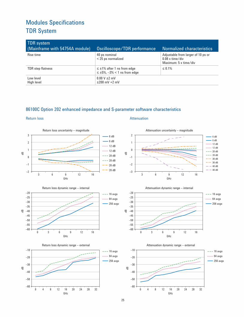
Modules SpecificationsTDR System
TDR system (Mainframe with 54754A module) Oscilloscope/TDR performance Normalized characteristicsRise time 40 ps nominal
< 25 ps normalizedAdjustable from larger of 10 ps or 0.08 x time/div Maximum: 5 x time/div
TDR step flatness ≤ ±1% after 1 ns from edge≤ ±5%, –3% < 1 ns from edge
≤ 0.1%
Low levelHigh level
0.00 V ±2 mV±200 mV +2 mV
86100C Option 202 enhanced impedance and S-parameter software characteristics
Return loss Attenuation
Return loss uncertainty – magnitude
GHz
dB
3
2
1
0
–1
–2
6 dB6 dB12 dB12 dB20 dB20 dB26 dB26 dB
3 6 9 12 16
Return loss dynamic range – internal
GHz
dB
–20–25–30–35–40–45–50–55–60
16 avgs64 avgs256 avgs
0 3 6 9 12 16
Return loss dynamic range – external
GHz
dB
–10
–20
–30
–40
–50
–60
16 avgs64 avgs256 avgs
0 4 8 12 16 20 24 28 32
Attenuation uncertainty – magnitude
GHz
dB
2
1
0
–1
–2
–3
6 dB6 dB12 dB12 dB20 dB20 dB30 dB30 dB40 dB40 dB
3 6 9 12 16
Attenuation dynamic range – internal
GHz
dB
–20–25–30–35–40–45–50–55–60
16 avgs64 avgs256 avgs
0 3 6 9 12 16
Attenuation dynamic range – external
GHz
dB
–10
–20
–30
–40
–50
–60
16 avgs64 avgs256 avgs
0 4 8 12 16 20 24 28 32
26
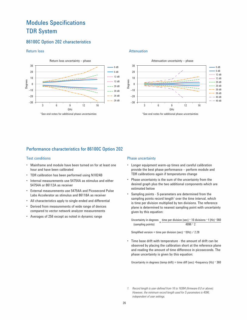
Modules SpecificationsTDR System86100C Option 202 characteristics
Return loss Attenuation
Return loss uncertainty – phase
*See end notes for additional phase uncertaintiesGHz
Degr
ees
30
20
10
0
–10
–20
–30
6 dB
6 dB
12 dB
12 dB
20 dB
20 dB
26 dB
26 dB
3 6 9 12 16
Attenuation uncertainty – phase
*See end notes for additional phase uncertaintiesGHz
Degr
ees
30
20
10
0
–10
–20
–30
6 dB6 dB12 dB12 dB20 dB20 dB30 dB30 dB40 dB40 dB
3 6 9 12 16
Test conditions• Mainframe and module have been turned on for at least one
hour and have been calibrated• TDR calibration has been performed using N1024B• Internal measurements use 54754A as stimulus and either
54754A or 86112A as receiver• External measurements use 54754A and Picosecond Pulse
Labs Accelerator as stimulus and 86118A as receiver• All characteristics apply to single-ended and differential• Derived from measurements of wide range of devices
compared to vector network analyzer measurements• Averages of 256 except as noted in dynamic range
Phase uncertainty• Longer equipment warm-up times and careful calibration
provide the best phase performance – perform module and TDR calibrations again if temperatures change
• Phase uncertainty is the sum of the uncertainty from the desired graph plus the two additional components which are estimated below
• Sampling points - S-parameters are determined from the sampling points record length1 over the time interval, which is time per division multiplied by ten divisions. The reference plane is determined to nearest sampling point with uncertainty given by this equation:
Uncertainty in degrees =
time per division (sec) * 10 divisions * f (Hz) *360 (sampling points) 4096 * 2
Simplified version = time per division (sec) * f(Hz) / 2.28
• Time base drift with temperature - the amount of drift can be observed by placing the calibration short at the reference plane and reading the amount of time difference in picoseconds. The phase uncertainty is given by this equation:
Uncertaintyindegrees(tempdrift)=timediff(sec)•frequency(Hz)* 360
Performance characteristics for 86100C Option 202
1. Record length is user-defined from 16 to 16384 (firmware 8.0 or above). However, the minimum record length used for S-parameters is 4096, independent of user settings.
27
Modules Specifications
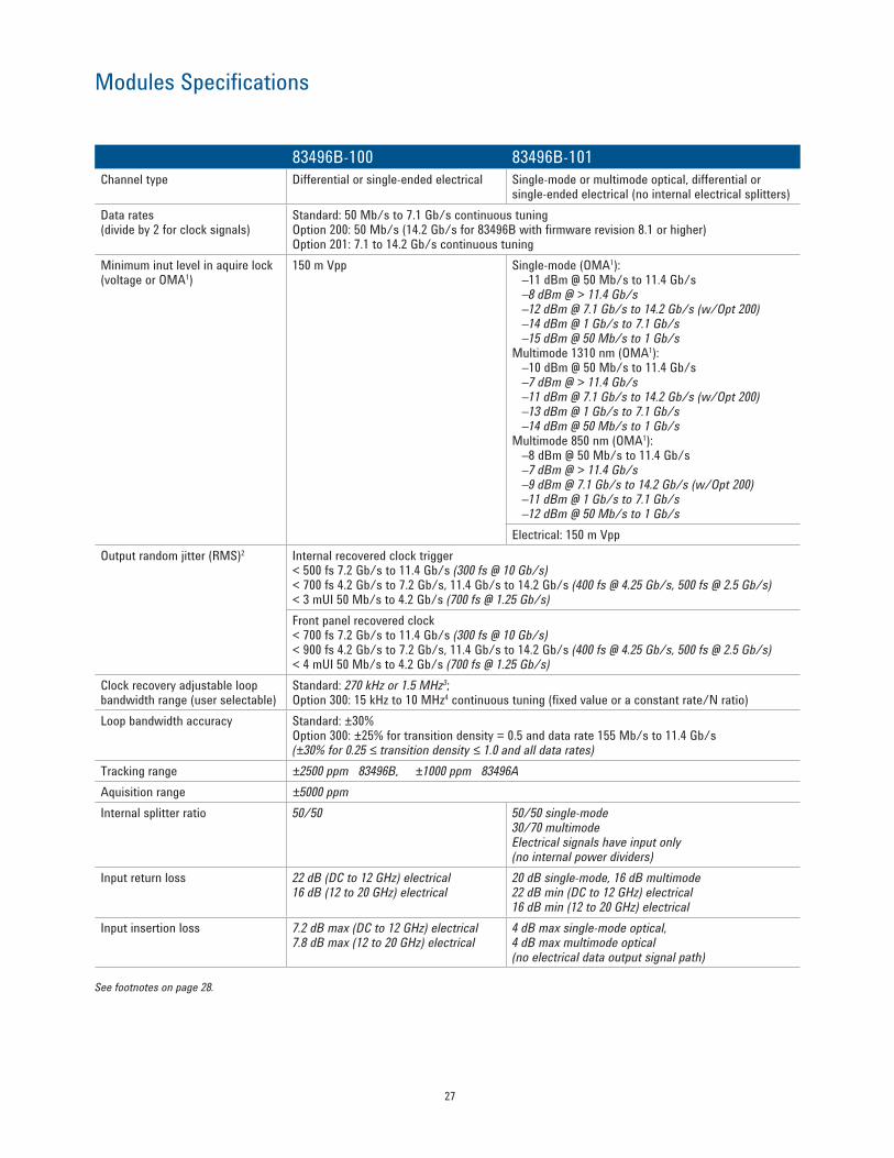
83496B-100 83496B-101Channel type Differential or single-ended electrical Single-mode or multimode optical, differential or
single-ended electrical (no internal electrical splitters)Data rates (divide by 2 for clock signals)
Standard: 50 Mb/s to 7.1 Gb/s continuous tuning Option 200: 50 Mb/s (14.2 Gb/s for 83496B with firmware revision 8.1 or higher) Option 201: 7.1 to 14.2 Gb/s continuous tuning
Minimum inut level in aquire lock(voltage or OMA1)
150 m Vpp Single-mode (OMA1): –11 dBm @ 50 Mb/s to 11.4 Gb/s –8 dBm @ > 11.4 Gb/s –12 dBm @ 7.1 Gb/s to 14.2 Gb/s (w/Opt 200) –14 dBm @ 1 Gb/s to 7.1 Gb/s –15 dBm @ 50 Mb/s to 1 Gb/sMultimode 1310 nm (OMA1): –10 dBm @ 50 Mb/s to 11.4 Gb/s –7 dBm @ > 11.4 Gb/s –11 dBm @ 7.1 Gb/s to 14.2 Gb/s (w/Opt 200) –13 dBm @ 1 Gb/s to 7.1 Gb/s –14 dBm @ 50 Mb/s to 1 Gb/sMultimode 850 nm (OMA1): –8 dBm @ 50 Mb/s to 11.4 Gb/s –7 dBm @ > 11.4 Gb/s –9 dBm @ 7.1 Gb/s to 14.2 Gb/s (w/Opt 200) –11 dBm @ 1 Gb/s to 7.1 Gb/s –12 dBm @ 50 Mb/s to 1 Gb/sElectrical: 150 m Vpp
Output random jitter (RMS)2 Internal recovered clock trigger< 500 fs 7.2 Gb/s to 11.4 Gb/s (300 fs @ 10 Gb/s)< 700 fs 4.2 Gb/s to 7.2 Gb/s, 11.4 Gb/s to 14.2 Gb/s (400 fs @ 4.25 Gb/s, 500 fs @ 2.5 Gb/s)< 3 mUI 50 Mb/s to 4.2 Gb/s (700 fs @ 1.25 Gb/s)Front panel recovered clock< 700 fs 7.2 Gb/s to 11.4 Gb/s (300 fs @ 10 Gb/s)< 900 fs 4.2 Gb/s to 7.2 Gb/s, 11.4 Gb/s to 14.2 Gb/s (400 fs @ 4.25 Gb/s, 500 fs @ 2.5 Gb/s)< 4 mUI 50 Mb/s to 4.2 Gb/s (700 fs @ 1.25 Gb/s)
Clock recovery adjustable loop bandwidth range (user selectable)
Standard: 270 kHz or 1.5 MHz3;Option 300: 15 kHz to 10 MHz4 continuous tuning (fixed value or a constant rate/N ratio)
Loop bandwidth accuracy Standard: ±30%Option 300: ±25% for transition density = 0.5 and data rate 155 Mb/s to 11.4 Gb/s(±30% for 0.25 ≤ transition density ≤ 1.0 and all data rates)
Tracking range ±2500 ppm 83496B, ±1000 ppm 83496AAquisition range ±5000 ppmInternal splitter ratio 50/50 50/50 single-mode
30/70 multimodeElectrical signals have input only(no internal power dividers)
Input return loss 22 dB (DC to 12 GHz) electrical16 dB (12 to 20 GHz) electrical
20 dB single-mode, 16 dB multimode22 dB min (DC to 12 GHz) electrical16 dB min (12 to 20 GHz) electrical
Input insertion loss 7.2 dB max (DC to 12 GHz) electrical7.8 dB max (12 to 20 GHz) electrical
4 dB max single-mode optical,4 dB max multimode optical(no electrical data output signal path)
See footnotes on page 28.
28
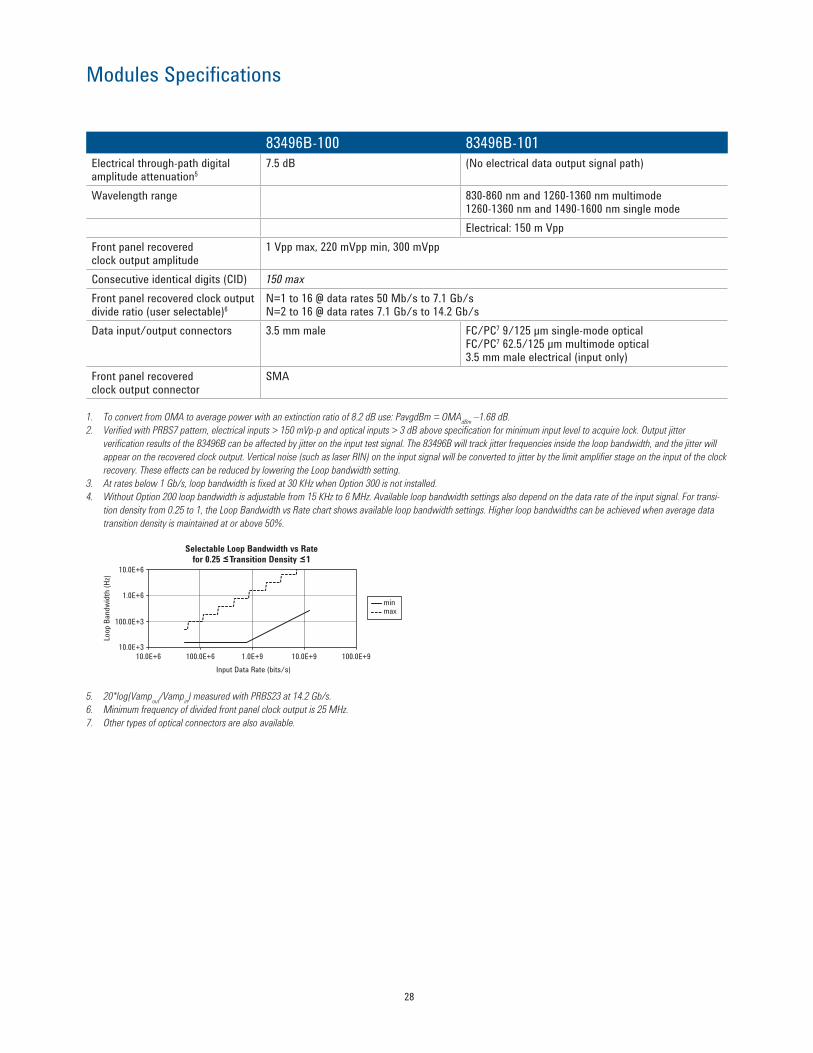
Modules Specifications
83496B-100 83496B-101Electrical through-path digitalamplitude attenuation5
7.5 dB (No electrical data output signal path)
Wavelength range 830-860 nm and 1260-1360 nm multimode1260-1360 nm and 1490-1600 nm single modeElectrical: 150 m Vpp
Front panel recoveredclock output amplitude
1 Vpp max, 220 mVpp min, 300 mVpp
Consecutive identical digits (CID) 150 maxFront panel recovered clock outputdivide ratio (user selectable)6
N=1 to 16 @ data rates 50 Mb/s to 7.1 Gb/sN=2 to 16 @ data rates 7.1 Gb/s to 14.2 Gb/s
Data input/output connectors 3.5 mm male FC/PC7 9/125 μm single-mode opticalFC/PC7 62.5/125 μm multimode optical3.5 mm male electrical (input only)
Front panel recoveredclock output connector
SMA
1. To convert from OMA to average power with an extinction ratio of 8.2 dB use: PavgdBm = OMAdBm –1.68 dB.2. Verified with PRBS7 pattern, electrical inputs > 150 mVp-p and optical inputs > 3 dB above specification for minimum input level to acquire lock. Output jitter
verification results of the 83496B can be affected by jitter on the input test signal. The 83496B will track jitter frequencies inside the loop bandwidth, and the jitter will appear on the recovered clock output. Vertical noise (such as laser RIN) on the input signal will be converted to jitter by the limit amplifier stage on the input of the clock recovery. These effects can be reduced by lowering the Loop bandwidth setting.
3. At rates below 1 Gb/s, loop bandwidth is fixed at 30 KHz when Option 300 is not installed.4. Without Option 200 loop bandwidth is adjustable from 15 KHz to 6 MHz. Available loop bandwidth settings also depend on the data rate of the input signal. For transi-
tion density from 0.25 to 1, the Loop Bandwidth vs Rate chart shows available loop bandwidth settings. Higher loop bandwidths can be achieved when average data transition density is maintained at or above 50%.
5. 20*log(Vampout/Vampin) measured with PRBS23 at 14.2 Gb/s.6. Minimum frequency of divided front panel clock output is 25 MHz.7. Other types of optical connectors are also available.
Selectable Loop Bandwidth vs Ratefor 0.25 Transition Density 1
10.0E+3
100.0E+3
1.0E+6
10.0E+6
10.0E+6 100.0E+6 1.0E+9 10.0E+9 100.0E+9Input Data Rate (bits/s)
Loop
Ban
dwidt
h (H
z)
minmax
29
Ordering Information
86100C Infiniium DCA-J mainframe86100C-001 Enhanced trigger86100CS-001 Enhanced trigger upgrade kit86100C-061 MATLAB - Basic Oscilloscope Package86100C-062 MATLAB - Standard Oscilloscope Package86100C-701 Standard trigger (default)86100C-090 Removable hard drive86100C-092 Internal hard drive (default)86100C-200 Jitter analysis software86100CU-200 Enhanced Jitter analysis software upgrade86100C-201 Advanced waveform analysis software86100CU-201 Advanced waveform analysis software upgrade86100C-202 Enhanced impedance and S-parameter software86100CU-202 Enhanced impedance and S-parameter software upgrade86100C-300 Amplitude analysis/RIN/Q-factor86100CU-300 Amplitude analysis/RIN/Q-factor upgrade86100CU-400 PLL and Jitter Spectrum software86100CU-401 Advanced EYE analysis software86100C-AFP Module slot filler panel86100C-AX4 Rack mount flange kit86100C-AXE Rack mount flange kit with handles86100C-UK6 Commercial cal certificate with test data
NOTE: Options 200 and 201 require Option 001 (enhanced trigger). Option 300 requires Options 200 and 001. Option 400 and 401 require Microsoft Office Excel 2003/2007. Option 401 requires Options 001/200 for DDPWS measurement. Options 610 and 620 require a 54754A module and Option 202.
Optical/electrical modules86105C 9 GHz optical channel; single-mode and multimode, amplified (750 to 1650 nm) 20 GHz electrical channel86105C-100 155 Mb/s through 8.5 Gb/s (choose 4 filter rates from Options 86105C-110 through 86105C-195)86105C-110 155 Mb/s86105C-120 622 Mb/s (also covers 614 Mb/s)86105C-130 1.063 Gb/s86105C-140 1.244/1.250 Gb/s (also covers 1.229 Mb/s)86105C-150 2.125 Gb/s86105C-160 2.488/2.500 Gb/s (also covers 2.458 Gb/s) 86105C-170 2.666 Gb/s
86105C-180 3.125 Gb/s (also covers 3.072 Gb/s)86105C-190 4.250 Gb/s86105C-193 5.0 Gb/s86105C-195 6.250 Gb/s (also covers 6.144 Gb/s) 86105C-200 8.5, 9.953, 10.3125, 10.519, 10.664, 10.709, 11.096, 11.317 Gb/s86105C-300 Combination of rates available in 86105C-100 and 86105C-200
86105D2 20 GHz optical channel; single-mode and multimode, (750-1650 nm); filters for 8.5, 9.953, 10.3125, 10.519, 10.664, 10.709, 11.096, 11.317, 14.025 Gb/s; 35 GHz electrical channel
86115D2 20 GHz multi-optical port plug-in module; single-mode and multimode (750-1650 nm); filters for 8.5, 9.953, 10.3125, 10.519, 10.664, 10.709, 11.096, 11.317, 14.925 Gb/s86115D-002 Two optical channels86115D-004 Four optical ports mulitplexed to two optical channels through 2 integral 1X2 optical switches
86116C2 40 to 65 GHz optical / 80 GHz electrical sampling module, 1300 to 1620 nm
Select exactly one reference receiver option:86116C-025: 40 GHz opt./80 GHz elec. channels, 17.0/25.8/27.7 Gb/s reference receiver86116C-041: 65 GHz opt./80 GHz elec. channels, 39.81/41.25/43.02 Gb/s reference receiver
This module is not compatible with the 86100A and 86100B DCA mainframes. If you want to upgrade older DCAs, contact Agilent Technologies to discuss current trade-in deals.
All optical modules have FC/PC connectors installed on each optical port. Other connector adapters available as options are: Diamond HMS-10, DIN, ST and SC.
1. 86105C Option 197 provides a 6.375 GHz BT filter and is compatible with early drafts of the 8X Fibre Channel standard. The final version of INCITS FC-PI-4 requires compliance test to be done with the 10.3125 Gb/s Ethernet filter that is provided only in Options 200 or 300.
2. This module is not compatible with the 86100A and 86100B DCA mainframes. If you want to upgrade older DCAs, contact Agilent Technologies to discuss current trade-in deals.
30
Ordering Information
Dual electrical channel modules86112A Dual 20 GHz electrical channels86117A Dual 50 GHz electrical channels86118A Dual 70 GHz electrical remote sampling channels86118A-H01 Differential De-SkewTDR/TDT modulesIncluded with each of these TDR modules is a TDR trigger cable, two 50 Ω SMA terminations and one SMA short.
54754A Differential TDR module with dual 18 GHz TDR/electrical channelsN1020A 6 GHz TDR probe kitN1021B 18 GHz Differential TDR Probe KitN1024B TDR Calibration kit
Precision timebase module86107A Precision timebase reference module 86107A-010 2.5 and 10 GHz clock input capability 86107A-020 10 and 20 GHz clock input capability 86107A-040 10, 20 and 40 GHz clock input capability
Clock recovery modulesThe following modules provide a recovered clock from the data signal for triggering at indicated data rates:
83496B 50 Mb/s to 7.1 Gb/s Clock recovery module. This module is not compatible with the 86100A and 86100B DCA mainframes. If you want to upgrade older DCAs, contact Agilent Technologies and ask for current trade-in deals. 83496B-100 Single-ended and differential electrical with integrated signal taps 83496B-101 Single Mode (1260-1360 nm and 1490-1600 nm) and multimode (830-860 nm and 1260-1360 nm) optical. Integrated signal taps. Single-ended or differential electrical inputs (no signal taps). 83496B-200 Increase operating range to 50 Mb/s to 14.2 Gb/s 83496BU-200 Upgrade data rate 0.05 Gb/s to 14.2 Gb/s83496B-201 Shift operating range to 7.1 to 14.2 Gb/s83496BU-201 Upgrade shift operating range to 7.1 to 14.2 Gb/s83496B-300 Add tunable loop bandwidth “golden PLL” capability 83496BU-300 Upgrade adjustable loop bandwidth
Precision waveform analyzer moduleDual electrical channel module with integrated clock recovery and precision timebase.
86108A-100 Dual 32 GHz electrical channels, integrated clock recovery (50 Mb/s to 14.2 Gb/s) with integrated precision timebase 86108A-001 Two 3.5 mm phase trimmers for skew adjustment
86108A-002 Two precision 3.5 mm 18 inch cables 86108A-003 Two 3.5 mm 3 dB attenuators 86108A-006 Two 3.5 mm 6 dB attenuators 86108A-010 Two 3.5 mm 10 dB attenuators 86108A-020 Two 3.5 mm 20 dB attenuators
Warranty options (for all products)R1280A Customer return repair service R1282A Customer return calibration service
Accessories11898A Extender module for plug-in modules 86101-60005 Filler panel 0960-2427 USB keyboard (included with 86100C) 1150-7799 USB mouse (included with 86100C) 9300-1308 ESD Heel strap 9300-1367 ESD Wrist strap 9300-1484 ESD Desk mat 9300-0980 ESD Wrist strap ground cord
Optical connector adaptersNote: Optical modules come standard with one FC/PC connector adapter
81000 AI Diamond HMS-10 connector 81000 FI FC/PC connector adapter 81000 SI DIN connector adapter 81000 VI ST connector adapter 81000 KI SC Connector adapter
RF/Microwave accessories11636B Power divider, DC to 26.5 GHz, APC 3.5 mm 11636C Power divider, DC to 50 GHz, 2.4 mm
11742A 45 MHz to 26.5 GHz DC blocking capacitor 11742A-K01 50 GHz DC blocking capacitor
8490D-020 2.4 mm 20 dB attenuator
11900B 2.4 mm (f-f) adapter 11901B 2.4 mm (f) to 3.5 mm (f) adapter 11901C 2.4 mm (m) to 3.5 mm (f) adapter 11901D 2.4 mm (f) to 3.5 mm (m) adapter 5061-5311 3.5 mm (f-f) adapter 1250-1158 SMA (f-f) adapter
1810-0118 3.5 mm termination 0960-0055 Short 1250-1666 SMA (f-f) adapter feedthru
31
Ordering Information
Passive probe54006A 6 GHz passive probe
Infiniimax I active probes (1.5 to 7 GHz)Note: The N1022B probe adapter is required to use these probes with the 86100 DCA
Infiniimax I probe amplifiersNote: Order one or more Infiniimax I probe head or connectivity kit for each amplifier
1130A 1.5 GHz probe amp1131A 3.5 GHz probe amp1132A 5 GHz Iprobe amp1134A 7 GHz probe amp
Infiniimax I probe headsE2675A InfiniiMax differential browser probe head and accessories. Includes 20 replaceable tips and ergonomic handle. Order E2658A for replacement accessories.E2676A InfiniiMax single-ended browser probe head and accessories. Includes two ground collar assemblies, 10 replaceable tips, a ground lead socket and ergonomic browser handle. Order E2663A for replacement accessories.E2677A InfiniiMax differential solder-in probe head and accessories. Includes 20 full bandwidth and 10 medium bandwidth damping resistors. Order E2670A for replacement accessories.E2678A InfiniiMax single-ended/differential socketed probe head and accessories. Includes 48 full bandwidth damping resistors, six damped wire accessories, four square pin sockets and socket heatshrink. Order E2671A for replacement accessories.E2679A InfiniiMax single-ended solder-in probe head and accessories. Includes 16 full bandwidth and eight medium bandwidth damping resistors and 24 zero ohm ground resistors. Order E2672A for replacement accessories.
Infiniimax I connectivity kits (popular collections of the aboveprobe heads)E2669A InfiniiMax connectivity kit for differential measurementsE2668A InfiniiMax connectivity kit for single-ended measurements
Infiniimax II active probes (10 to 13 GHz)Note: The N1022B probe adapter is required to use these probes with the 86100 DCA
Infiniimax II probe amplifiersNote: Order 1 or more Infiniimax II probe heads for each amplifier. Infiniimax I probe heads and connectivity kits can also be used but will have limited bandwidth.1168A 10 GHz probe amp1169A 13 GHz probe amp
Infiniimax II probe headsN5380A InfiniiMax II 12 GHz differential SMA adapterN5381A InfiniiMax II 12 GHz solder-in probe headN5382A InfiniiMax II 12 GHz differential browser
Probe adaptersN1022B Adapts 113x/115x,/116x active probes to 86100 Infiniium DCA
The N1022B adapter is powered by connecting it to the built-in probe power connector available on some DCA modules (see page 18 ), or to an external probe power supply. On modules that do not have a built-in probe power connector, use an 1143A external power supply. It is recommended to order option 001 on the 1143A, which provides a 5-foot power extension cable (01143-61602). The 1143A power supply can power two probes.
Connectivity solutionsHDMIN1080A H01 High performance coax based HDMI fixture with plug (TPA-P)N1080A H02 High performance coax based HDMI fixture with receptacle (TPA-R)N1080A H03 HDMI low frequency board
SATANote: These are available from COMAX Technology, see www.comaxtech.comiSATA plug to SMA – COMAX P/N H303000104iSATA receptacle to SMA – COMAX P/N H303000204
ATCANote: These are available from F9 Systems, see www.f9-systems.comAdvanced TCA Tx/Rx Signal Blade™Advanced TCA Tx/Rx Bench Blade™
Call Agilent for connectivity and probing solutions not listed above.
Firmware and softwareFirmware and software upgrades are available through the Web or your local sales office. www.agilent.com/find/dcaj
Windows is a U.S. registered trademark of Microsoft CorporationMATLAB is a U.S. registered trademark of The Math Works, Inc.
www.lxistandard.org LAN eXtensions for Instruments puts the power of Ethernet and the Web inside your test systems. Agilent is a founding member of the LXI consortium.
Agilent Channel Partnerswww.agilent.com/find/channelpartnersGet the best of both worlds: Agilent’s measurement expertise and product breadth, combined with channel partner convenience.
For more information on Agilent Technologies’ products, applications or services, please contact your local Agilent office. The complete list is available at:www.agilent.com/find/contactus
Americas Canada (877) 894 4414 Brazil (11) 4197 3600Mexico 01800 5064 800 United States (800) 829 4444
Asia Pacific Australia 1 800 629 485China 800 810 0189Hong Kong 800 938 693India 1 800 112 929Japan 0120 (421) 345Korea 080 769 0800Malaysia 1 800 888 848Singapore 1 800 375 8100Taiwan 0800 047 866Other AP Countries (65) 375 8100
Europe & Middle EastBelgium 32 (0) 2 404 93 40 Denmark 45 45 80 12 15Finland 358 (0) 10 855 2100France 0825 010 700* *0.125 €/minuteGermany 49 (0) 7031 464 6333 Ireland 1890 924 204Israel 972-3-9288-504/544Italy 39 02 92 60 8484Netherlands 31 (0) 20 547 2111Spain 34 (91) 631 3300Sweden 0200-88 22 55United Kingdom 44 (0) 118 927 6201For other unlisted countries: www.agilent.com/find/contactus(BP2-19-13)
Product specifications and descriptions in this document subject to change without notice.
© Agilent Technologies, Inc. 2012, 2013Published in USA, March 8, 20135989-0278EN
www.agilent.comwww.agilent.com/find/dcaj
www.agilent.com/quality
www.axiestandard.org AdvancedTCA® Extensions for Instrumentation and Test (AXIe) is an open standard that extends the AdvancedTCA for general purpose and semiconductor test. Agilent is a founding member of the AXIe consortium.
www.pxisa.org PCI eXtensions for Instrumentation (PXI) modular instrumentation delivers a rugged, PC-based high-performance measurement and automation system.
Quality Management SystemQuality Management SysISO 9001:2008Agilent Electronic Measurement Group
DEKRA Certified
www.agilent.com/find/myagilent A personalized view into the information most relevant to you.
myAgilentmyAgilent
www.agilent.com/find/AdvantageServicesAccurate measurements throughout the life of your instruments.
Agilent Advantage Services
Three-Year Warranty
www.agilent.com/find/ThreeYearWarrantyAgilent’s combination of product reliability and three-year warranty coverage is another way we help you achieve your business goals: increased confidence in uptime, reduced cost of ownership and greater convenience.