datasheet - intersil · cmos programmable interval timer ... - enhanced version of nmos 8253 ......
TRANSCRIPT
FN2970Rev 6.00
Sep 15, 2015
82C54CMOS Programmable Interval Timer
DATASHEET
The Intersil 82C54 is a high performance CMOS Programmable Interval Timer manufactured using an advanced 2 micron CMOS process.
The 82C54 has three independently programmable and functional 16-bit counters, each capable of handling clock input frequencies of up to 8MHz (82C54) or 10MHz (82C54-10) or 12MHz (82C54-12).
The high speed and industry standard configuration of the 82C54 make it compatible with the Intersil 80C86, 80C88, and 80C286 CMOS microprocessors along with many other industry standard processors. Six programmable timer modes allow the 82C54 to be used as an event counter, elapsed time indicator, programmable one-shot, and many other applications. Static CMOS circuit design insures low power operation.
The Intersil advanced CMOS process results in a significant reduction in power with performance equal to or greater than existing equivalent products.
Features
• 8MHz to 12MHz Clock Input Frequency
• Compatible with NMOS 8254
- Enhanced Version of NMOS 8253
• Three Independent 16-Bit Counters
• Six Programmable Counter Modes
• Status Read Back Command
• Binary or BCD Counting
• Fully TTL Compatible
• Single 5V Power Supply
• Low Power
- ICCSB. . . . . . . . . . . . . . . . . . . . . . . . . . . . . . . . . . .10µA
- ICCOP . . . . . . . . . . . . . . . . . . . . . . . . . . 10mA at 8MHz
• Operating Temperature Ranges
- CX82C54 . . . . . . . . . . . . . . . . . . . . . . . . . 0°C to +70°C
- IX82C54 . . . . . . . . . . . . . . . . . . . . . . . . . -40°C to +85°C
- MD82C54 . . . . . . . . . . . . . . . . . . . . . . . -55°C to +125°C
• Pb-Free Plus Anneal Available (RoHS Compliant)
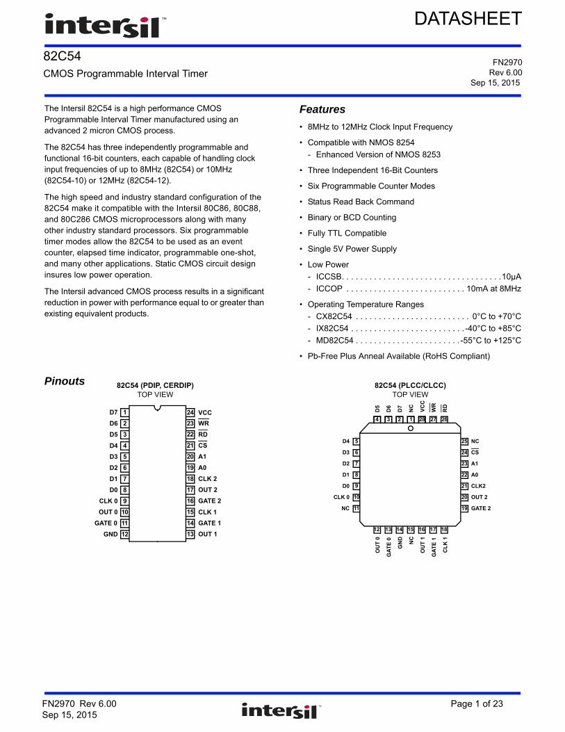
Pinouts 82C54 (PDIP, CERDIP)TOP VIEW
82C54 (PLCC/CLCC)TOP VIEW
1
2
3
4
5
6
7
8
9
10
11
12
16
17
18
19
20
21
22
23
24
15
14
13
D7
D6
D5
D4
D3
D2
D1
D0
CLK 0
OUT 0
GATE 0
GND
VCC
RD
CS
A1
A0
OUT 2
CLK 1
GATE 1
OUT 1
WR
CLK 2
GATE 2
GN
D
NC
OU
T 1
GA
TE
1
CL
K 1
OU
T 0
GA
TE
0
D7
NC
VC
C
WR
RD
D5
D6
CS
A1
A0
CLK2
NC
GATE 2
OUT 2
1234
5
6
7
8
9
10
11
12 13 14 15 16 17 18
19
20
21
22
23
24
25
262728
D3
D2
D1
D0
D4
NC
CLK 0
FN2970 Rev 6.00 Page 1 of 23Sep 15, 2015
82C54
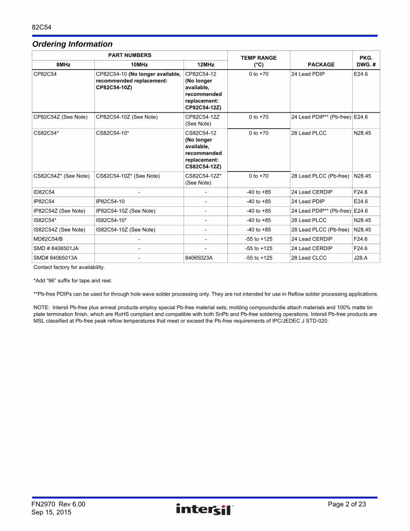
Ordering InformationPART NUMBERS TEMP RANGE
(°C) PACKAGEPKG.
DWG. #8MHz 10MHz 12MHz
CP82C54 CP82C54-10 (No longer available, recommended replacement: CP82C54-10Z)
CP82C54-12 (No longer available, recommended replacement: CP82C54-12Z)
0 to +70 24 Lead PDIP E24.6
CP82C54Z (See Note) CP82C54-10Z (See Note) CP82C54-12Z (See Note)
0 to +70 24 Lead PDIP** (Pb-free) E24.6
CS82C54* CS82C54-10* CS82C54-12 (No longer available, recommended replacement: CS82C54-12Z)
0 to +70 28 Lead PLCC N28.45
CS82C54Z* (See Note) CS82C54-10Z* (See Note) CS82C54-12Z* (See Note)
0 to +70 28 Lead PLCC (Pb-free) N28.45
ID82C54 - - -40 to +85 24 Lead CERDIP F24.6
IP82C54 IP82C54-10 - -40 to +85 24 Lead PDIP E24.6
IP82C54Z (See Note) IP82C54-10Z (See Note) - -40 to +85 24 Lead PDIP** (Pb-free) E24.6
IS82C54* IS82C54-10* - -40 to +85 28 Lead PLCC N28.45
IS82C54Z (See Note) IS82C54-10Z (See Note) - -40 to +85 28 Lead PLCC (Pb-free) N28.45
MD82C54/B - - -55 to +125 24 Lead CERDIP F24.6
SMD # 8406501JA - - -55 to +125 24 Lead CERDIP F24.6
SMD# 84065013A - 84065023A -55 to +125 28 Lead CLCC J28.A
Contact factory for availability.
*Add “96” suffix for tape and reel.
**Pb-free PDIPs can be used for through hole wave solder processing only. They are not intended for use in Reflow solder processing applications.
NOTE: Intersil Pb-free plus anneal products employ special Pb-free material sets; molding compounds/die attach materials and 100% matte tin plate termination finish, which are RoHS compliant and compatible with both SnPb and Pb-free soldering operations. Intersil Pb-free products are MSL classified at Pb-free peak reflow temperatures that meet or exceed the Pb-free requirements of IPC/JEDEC J STD-020.
FN2970 Rev 6.00 Page 2 of 23Sep 15, 2015

82C54
Absolute Maximum Ratings Thermal Information
Supply Voltage . . . . . . . . . . . . . . . . . . . . . . . . . . . . . . . . . . . . . +8.0VInput, Output or I/O Voltage . . . . . . . . . . . . GND-0.5V to VCC +0.5VESD Classification . . . . . . . . . . . . . . . . . . . . . . . . . . . . . . . . . Class 1
Operating ConditionsOperating Voltage Range. . . . . . . . . . . . . . . . . . . . . . +4.5V to +5.5VOperating Temperature Range
CX82C54 . . . . . . . . . . . . . . . . . . . . . . . . . . . . . . . . . 0°C to +70°CIX82C54 . . . . . . . . . . . . . . . . . . . . . . . . . . . . . . . . .-40°C to +85°CMD82C54 . . . . . . . . . . . . . . . . . . . . . . . . . . . . . . .-55°C to +125°C
Thermal Resistance (Typical) JA (oC/W) JC (oC/W)
CERDIP Package. . . . . . . . . . . . . . . . . 55 12CLCC Package . . . . . . . . . . . . . . . . . . 65 14PDIP Package* . . . . . . . . . . . . . . . . . . 55 N/APLCC Package. . . . . . . . . . . . . . . . . . . 60 N/A
Storage Temperature Range . . . . . . . . . . . . . . . . . . -65°C to +150°CMaximum Junction Temperature Ceramic Package . . . . . . . +175°CMaximum Junction Temperature Plastic Package . . . . . . . . . +150°CMaximum Lead Temperature Package (Soldering 10s). . . . . +300°C
(PLCC - Lead Tips Only)
*Pb-free PDIPs can be used for through hole wave solderprocessing only. They are not intended for use in Reflow solderprocessing applications.
Die CharacteristicsGate Count . . . . . . . . . . . . . . . . . . . . . . . . . . . . . . . . . . .2250 Gates
CAUTION: Stresses above those listed in “Absolute Maximum Ratings” may cause permanent damage to the device. This is a stress only rating and operation of thedevice at these or any other conditions above those indicated in the operational sections of this specification is not implied.
DC Electrical Specifications VCC = +5.0V ± 10%, Includes all Temperature Ranges
SYMBOL PARAMETER MIN MAX UNITS TEST CONDITIONS
VIH Logical One Input Voltage 2.0 - V CX82C54, IX82C54
2.2 - V MD82C54
VIL Logical Zero Input Voltage - 0.8 V -
VOH Output HIGH Voltage 3.0 - V IOH = -2.5mA
VCC -0.4 - V IOH = -100A
VOL Output LOW Voltage - 0.4 V IOL = +2.5mA
II Input Leakage Current -1 +1 A VIN = GND or VCCDIP Pins 9,11,14-16,18-23
IO Output Leakage Current -10 +10 A VOUT = GND or VCCDIP Pins 1-8
ICCSB Standby Power Supply Current - 10 A VCC = 5.5V, VIN = GND or VCC, Outputs Open, CountersProgrammed
ICCOP Operating Power Supply Current - 10 mA VCC = 5.5V,CLK0 = CLK1 = CLK2 = 8MHz,VIN = GND or VCC,Outputs Open
Capacitance TA = +25oC; All Measurements Referenced to Device GND, Note 1
SYMBOL PARAMETER TYP UNITS TEST CONDITIONS
CIN Input Capacitance 20 pF FREQ = 1MHz
COUT Output Capacitance 20 pF FREQ = 1MHz
CI/O I/O Capacitance 20 pF FREQ = 1MHz
NOTE:
1. Not tested, but characterized at initial design and at major process/design changes.
FN2970 Rev 6.00 Page 3 of 23Sep 15, 2015
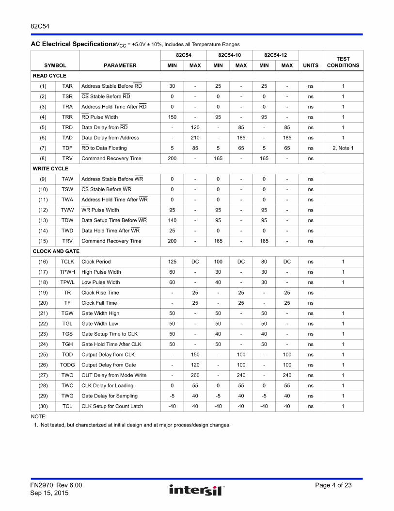
82C54
AC Electrical SpecificationsVCC = +5.0V ± 10%, Includes all Temperature Ranges
SYMBOL PARAMETER
82C54 82C54-10 82C54-12
UNITSTEST
CONDITIONSMIN MAX MIN MAX MIN MAX
READ CYCLE
(1) TAR Address Stable Before RD 30 - 25 - 25 - ns 1
(2) TSR CS Stable Before RD 0 - 0 - 0 - ns 1
(3) TRA Address Hold Time After RD 0 - 0 - 0 - ns 1
(4) TRR RD Pulse Width 150 - 95 - 95 - ns 1
(5) TRD Data Delay from RD - 120 - 85 - 85 ns 1
(6) TAD Data Delay from Address - 210 - 185 - 185 ns 1
(7) TDF RD to Data Floating 5 85 5 65 5 65 ns 2, Note 1
(8) TRV Command Recovery Time 200 - 165 - 165 - ns
WRITE CYCLE
(9) TAW Address Stable Before WR 0 - 0 - 0 - ns
(10) TSW CS Stable Before WR 0 - 0 - 0 - ns
(11) TWA Address Hold Time After WR 0 - 0 - 0 - ns
(12) TWW WR Pulse Width 95 - 95 - 95 - ns
(13) TDW Data Setup Time Before WR 140 - 95 - 95 - ns
(14) TWD Data Hold Time After WR 25 - 0 - 0 - ns
(15) TRV Command Recovery Time 200 - 165 - 165 - ns
CLOCK AND GATE
(16) TCLK Clock Period 125 DC 100 DC 80 DC ns 1
(17) TPWH High Pulse Width 60 - 30 - 30 - ns 1
(18) TPWL Low Pulse Width 60 - 40 - 30 - ns 1
(19) TR Clock Rise Time - 25 - 25 - 25 ns
(20) TF Clock Fall Time - 25 - 25 - 25 ns
(21) TGW Gate Width High 50 - 50 - 50 - ns 1
(22) TGL Gate Width Low 50 - 50 - 50 - ns 1
(23) TGS Gate Setup Time to CLK 50 - 40 - 40 - ns 1
(24) TGH Gate Hold Time After CLK 50 - 50 - 50 - ns 1
(25) TOD Output Delay from CLK - 150 - 100 - 100 ns 1
(26) TODG Output Delay from Gate - 120 - 100 - 100 ns 1
(27) TWO OUT Delay from Mode Write - 260 - 240 - 240 ns 1
(28) TWC CLK Delay for Loading 0 55 0 55 0 55 ns 1
(29) TWG Gate Delay for Sampling -5 40 -5 40 -5 40 ns 1
(30) TCL CLK Setup for Count Latch -40 40 -40 40 -40 40 ns 1
NOTE:
1. Not tested, but characterized at initial design and at major process/design changes.
FN2970 Rev 6.00 Page 4 of 23Sep 15, 2015
82C54
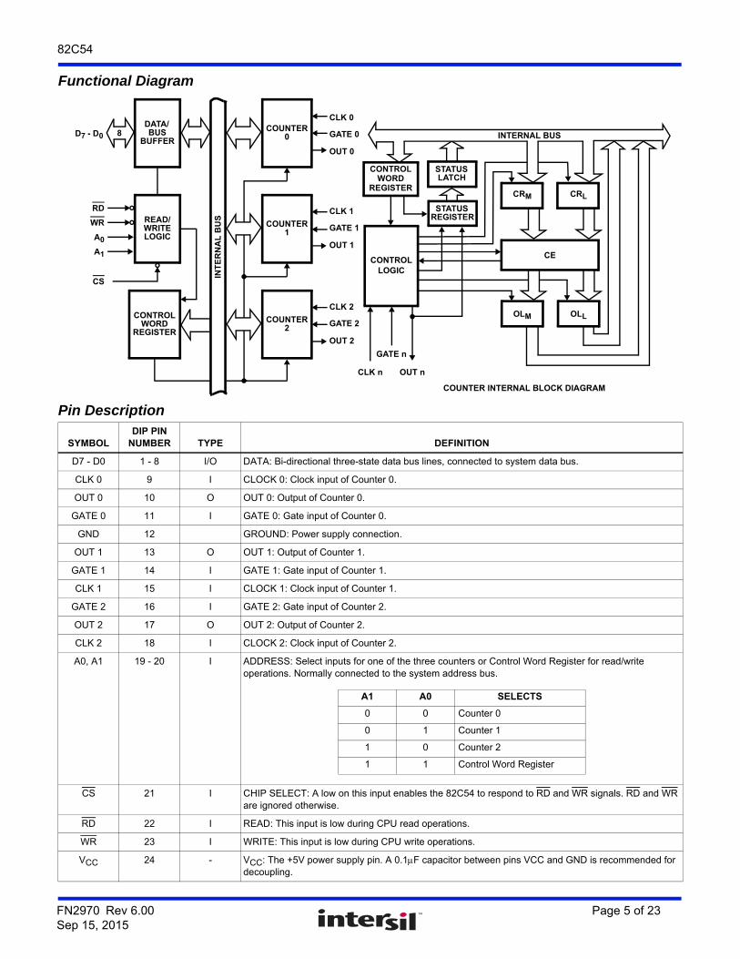
Functional Diagram
CONTROLWORD
REGISTER
READ/WRITELOGIC
DATA/BUS
BUFFER
COUNTER2
COUNTER1
COUNTER0
INT
ER
NA
L B
US
INTERNAL BUS
CONTROLLOGIC
CONTROLWORD
REGISTER
STATUSLATCH
STATUSREGISTER
CLK n
GATE n
OUT n
OUT 2
GATE 2
CLK 2
OUT 1
GATE 1
CLK 1
OUT 0
GATE 0
CLK 0
WR
RD
D7 - D0
A0
A1
CS
OLM OLL
CE
CRM CRL
COUNTER INTERNAL BLOCK DIAGRAM
8
Pin Description
SYMBOLDIP PIN
NUMBER TYPE DEFINITION
D7 - D0 1 - 8 I/O DATA: Bi-directional three-state data bus lines, connected to system data bus.
CLK 0 9 I CLOCK 0: Clock input of Counter 0.
OUT 0 10 O OUT 0: Output of Counter 0.
GATE 0 11 I GATE 0: Gate input of Counter 0.
GND 12 GROUND: Power supply connection.
OUT 1 13 O OUT 1: Output of Counter 1.
GATE 1 14 I GATE 1: Gate input of Counter 1.
CLK 1 15 I CLOCK 1: Clock input of Counter 1.
GATE 2 16 I GATE 2: Gate input of Counter 2.
OUT 2 17 O OUT 2: Output of Counter 2.
CLK 2 18 I CLOCK 2: Clock input of Counter 2.
A0, A1 19 - 20 I ADDRESS: Select inputs for one of the three counters or Control Word Register for read/writeoperations. Normally connected to the system address bus.
CS 21 I CHIP SELECT: A low on this input enables the 82C54 to respond to RD and WR signals. RD and WR are ignored otherwise.
RD 22 I READ: This input is low during CPU read operations.
WR 23 I WRITE: This input is low during CPU write operations.
VCC 24 - VCC: The +5V power supply pin. A 0.1F capacitor between pins VCC and GND is recommended for decoupling.
A1 A0 SELECTS
0 0 Counter 0
0 1 Counter 1
1 0 Counter 2
1 1 Control Word Register
FN2970 Rev 6.00 Page 5 of 23Sep 15, 2015
82C54
Functional Description
General
The 82C54 is a programmable interval timer/counter designed for use with microcomputer systems. It is a general purpose, multi-timing element that can be treated as an array of I/O ports in the system software.
The 82C54 solves one of the most common problems in any microcomputer system, the generation of accurate time delays under software control. Instead of setting up timing loops in software, the programmer configures the 82C54 to match his requirements and programs one of the counters for the desired delay. After the desired delay, the 82C54 will interrupt the CPU. Software overhead is minimal and variable length delays can easily be accommodated.
Some of the other computer/timer functions common to microcomputers which can be implemented with the 82C54 are:
• Real time clock
• Event counter
• Digital one-shot
• Programmable rate generator
• Square wave generator
• Binary rate multiplier
• Complex waveform generator
• Complex motor controller
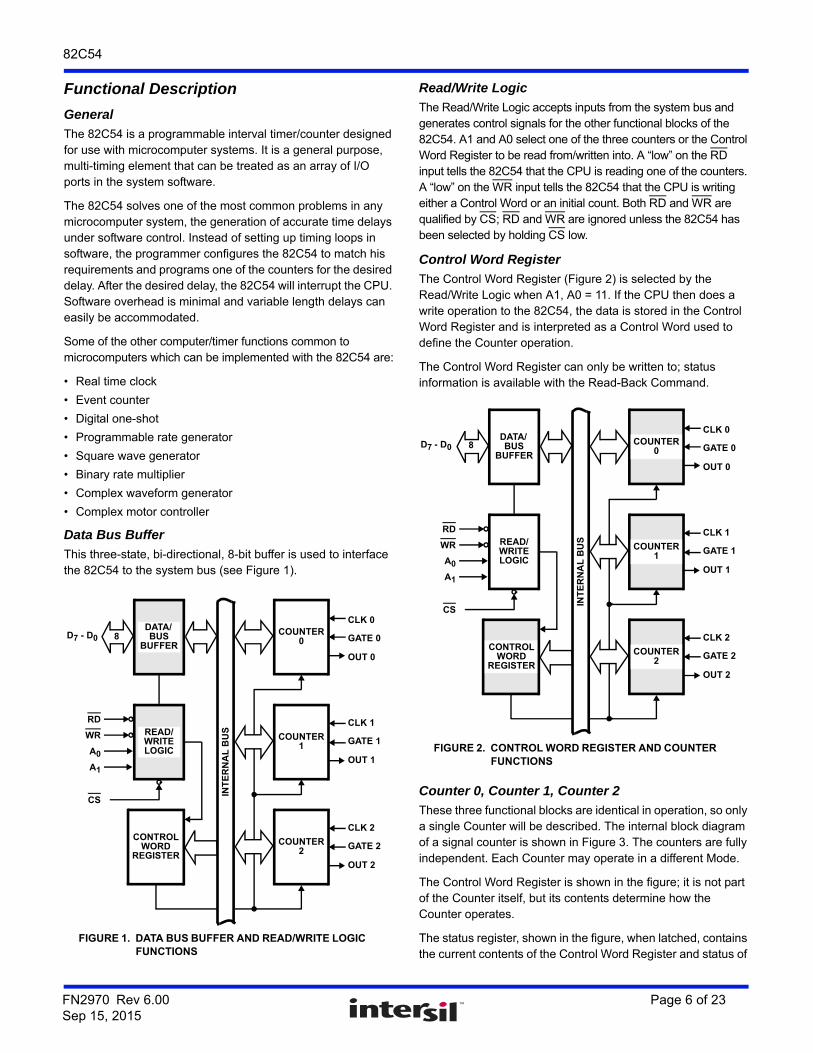
Data Bus Buffer
This three-state, bi-directional, 8-bit buffer is used to interface the 82C54 to the system bus (see Figure 1).
Read/Write Logic
The Read/Write Logic accepts inputs from the system bus and generates control signals for the other functional blocks of the 82C54. A1 and A0 select one of the three counters or the Control Word Register to be read from/written into. A “low” on the RD input tells the 82C54 that the CPU is reading one of the counters. A “low” on the WR input tells the 82C54 that the CPU is writing either a Control Word or an initial count. Both RD and WR are qualified by CS; RD and WR are ignored unless the 82C54 has been selected by holding CS low.
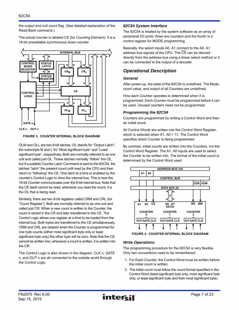
Control Word Register
The Control Word Register (Figure 2) is selected by the Read/Write Logic when A1, A0 = 11. If the CPU then does a write operation to the 82C54, the data is stored in the Control Word Register and is interpreted as a Control Word used to define the Counter operation.
The Control Word Register can only be written to; status information is available with the Read-Back Command.
Counter 0, Counter 1, Counter 2
These three functional blocks are identical in operation, so only a single Counter will be described. The internal block diagram of a signal counter is shown in Figure 3. The counters are fully independent. Each Counter may operate in a different Mode.
The Control Word Register is shown in the figure; it is not part of the Counter itself, but its contents determine how the Counter operates.
The status register, shown in the figure, when latched, contains the current contents of the Control Word Register and status of
CONTROLWORD
REGISTER
COUNTER2
COUNTER1
COUNTER0
INT
ER
NA
L B
US
OUT 2
GATE 2
CLK 2
OUT 1
GATE 1
CLK 1
OUT 0
GATE 0
CLK 0
WR
RD
D7 - D0
A0
A1
CS
FIGURE 1. DATA BUS BUFFER AND READ/WRITE LOGIC FUNCTIONS
8DATA/BUS
BUFFER
READ/WRITELOGIC
READ/WRITELOGIC
DATA/BUS
BUFFER
INT
ER
NA
L B
US
OUT 2
GATE 2
CLK 2
OUT 1
GATE 1
CLK 1
OUT 0
GATE 0
CLK 0
WR
RD
D7 - D0
A0
A1
CS
FIGURE 2. CONTROL WORD REGISTER AND COUNTER FUNCTIONS
8
CONTROLWORD
REGISTER
COUNTER2
COUNTER1
COUNTER0
FN2970 Rev 6.00 Page 6 of 23Sep 15, 2015
82C54
the output and null count flag. (See detailed explanation of the Read-Back command.)
The actual counter is labeled CE (for Counting Element). It is a 16-bit presettable synchronous down counter.
OLM and OLL are two 8-bit latches. OL stands for “Output Latch”; the subscripts M and L for “Most significant byte” and “Least significant byte”, respectively. Both are normally referred to as one unit and called just OL. These latches normally “follow” the CE, but if a suitable Counter Latch Command is sent to the 82C54, the latches “latch” the present count until read by the CPU and then return to “following” the CE. One latch at a time is enabled by the counter’s Control Logic to drive the internal bus. This is how the 16-bit Counter communicates over the 8-bit internal bus. Note that the CE itself cannot be read; whenever you read the count, it is the OL that is being read.
Similarly, there are two 8-bit registers called CRM and CRL (for “Count Register”). Both are normally referred to as one unit and called just CR. When a new count is written to the Counter, the count is stored in the CR and later transferred to the CE. The Control Logic allows one register at a time to be loaded from the internal bus. Both bytes are transferred to the CE simultaneously. CRM and CRL are cleared when the Counter is programmed for one byte counts (either most significant byte only or least significant byte only) the other byte will be zero. Note that the CE cannot be written into; whenever a count is written, it is written into the CR.
The Control Logic is also shown in the diagram. CLK n, GATE n, and OUT n are all connected to the outside world through the Control Logic.
82C54 System Interface
The 82C54 is treated by the system software as an array of peripheral I/O ports; three are counters and the fourth is a control register for MODE programming.
Basically, the select inputs A0, A1 connect to the A0, A1 address bus signals of the CPU. The CS can be derived directly from the address bus using a linear select method or it can be connected to the output of a decoder.
Operational Description
General
After power-up, the state of the 82C54 is undefined. The Mode, count value, and output of all Counters are undefined.
How each Counter operates is determined when it is programmed. Each Counter must be programmed before it can be used. Unused counters need not be programmed.
Programming the 82C54
Counters are programmed by writing a Control Word and then an initial count.
All Control Words are written into the Control Word Register, which is selected when A1, A0 = 11. The Control Word specifies which Counter is being programmed.
By contrast, initial counts are written into the Counters, not the Control Word Register. The A1, A0 inputs are used to select the Counter to be written into. The format of the initial count is determined by the Control Word used.
Write Operations
The programming procedure for the 82C54 is very flexible. Only two conventions need to be remembered:
1. For Each Counter, the Control Word must be written before the initial count is written.
2. The initial count must follow the count format specified in the Control Word (least significant byte only, most significant byte only, or least significant byte and then most significant byte).
INTERNAL BUS
CONTROLLOGIC
CONTROLWORD
REGISTER
STATUSLATCH
STATUSREGISTER
CLK n
GATE n
OUT n
OLM OLL
CE
CRM CRL
FIGURE 3. COUNTER INTERNAL BLOCK DIAGRAM
ADDRESS BUS (16)
CONTROL BUS
DATA BUS (8)
I/OR I/OW
WRRDCSA0A1
A1 A0
8
COUNTER0
OUTGATE CLK
COUNTER1
COUNTER2
OUTGATE CLK OUTGATE CLK
D0 - D782C54
FIGURE 4. COUNTER INTERNAL BLOCK DIAGRAM
FN2970 Rev 6.00 Page 7 of 23Sep 15, 2015
82C54
Since the Control Word Register and the three Counters have separate addresses (selected by the A1, A0 inputs), and each Control Word specifies the Counter it applies to (SC0, SC1 bits), no special instruction sequence is required. Any programming sequence that follows the conventions above is acceptable.
CONTROL WORD FORMAT
A1, A0 = 11; CS = 0; RD = 1; WR = 0
D7 D6 D5 D4 D3 D2 D1 D0
SC1 SC0 RW1 RW0 M2 M1 M0 BCD
SC - SELECT COUNTER
SC1 SC0
0 0 Select Counter 0
0 1 Select Counter 1
1 0 Select Counter 2
1 1 Read-Back Command (See Read Operations)
RW - READ/WRITE
RW1 RW0
0 0 Counter Latch Command (See Read Operations)
0 1 Read/Write least significant byte only.
1 0 Read/Write most significant byte only.
1 1 Read/Write least significant byte first, then mostsignificant byte.
M - MODE
M2 M1 M0
0 0 0 Mode 0
0 0 1 Mode 1
X 1 0 Mode 2
X 1 1 Mode 3
1 0 0 Mode 4
1 0 1 Mode 5
BCD - BINARY CODED DECIMAL
0 Binary Counter 16-bit
1 Binary Coded Decimal (BCD) Counter (4 Decades)
NOTE: Don’t Care bits (X) should be 0 to insure compatibility withfuture products.
POSSIBLE PROGRAMMING SEQUENCE
A1 A0
Control Word - Counter 0 1 1
LSB of Count - Counter 0 0 0
MSB of Count - Counter 0 0 0
Control Word - Counter 1 1 1
LSB of Count - Counter 1 0 1
MSB of Count - Counter 1 0 1
Control Word - Counter 2 1 1
LSB of Count - Counter 2 1 0
MSB of Count - Counter 2 1 0
POSSIBLE PROGRAMMING SEQUENCE
A1 A0
Control Word - Counter 0 1 1
Control Word - Counter 1 1 1
Control Word - Counter 2 1 1
LSB of Count - Counter 2 1 0
LSB of Count - Counter 1 0 1
LSB of Count - Counter 0 0 0
MSB of Count - Counter 0 0 0
MSB of Count - Counter 1 0 1
MSB of Count - Counter 2 1 0
POSSIBLE PROGRAMMING SEQUENCE
A1 A0
Control Word - Counter 2 1 1
Control Word - Counter 1 1 1
Control Word - Counter 0 1 1
LSB of Count - Counter 2 1 0
MSB of Count - Counter 2 1 0
LSB of Count - Counter 1 0 1
MSB of Count - Counter 1 0 1
LSB of Count - Counter 0 0 0
MSB of Count - Counter 0 0 0
FN2970 Rev 6.00 Page 8 of 23Sep 15, 2015
82C54
A new initial count may be written to a Counter at any time without affecting the Counter’s programmed Mode in any way. Counting will be affected as described in the Mode definitions. The new count must follow the programmed count format.
If a Counter is programmed to read/write two-byte counts, the following precaution applies. A program must not transfer control between writing the first and second byte to another routine which also writes into that same Counter. Otherwise, the Counter will be loaded with an incorrect count.
READ OPERATIONS
It is often desirable to read the value of a Counter without disturbing the count in progress. This is easily done in the 82C54.
There are three possible methods for reading the Counters. The first is through the Read-Back command, which is explained later. The second is a simple read operation of the Counter, which is selected with the A1, A0 inputs. The only requirement is that the CLK input of the selected Counter must be inhibited by using either the GATE input or external logic. Otherwise, the count may be in process of changing when it is read, giving an undefined result.
COUNTER LATCH COMMAND
The other method for reading the Counters involves a special software command called the “Counter Latch Command”. Like a Control Word, this command is written to the Control Word Register, which is selected when A1, A0 = 11. Also, like a Control Word, the SC0, SC1 bits select one of the three Counters, but two other bits, D5 and D4, distinguish this command from a Control Word.
.
The selected Counter’s output latch (OL) latches the count when the Counter Latch Command is received. This count is held in the latch until it is read by the CPU (or until the Counter is reprogrammed). The count is then unlatched automatically and the OL returns to “following” the counting element (CE). This allows reading the contents of the Counters “on the fly” without affecting counting in progress. Multiple Counter Latch Commands may be used to latch more than one Counter. Each latched Counter’s OL holds its count until read. Counter Latch Commands do not affect the programmed Mode of the Counter in any way.
If a Counter is latched and then, some time later, latched again before the count is read, the second Counter Latch Command is ignored. The count read will be the count at the time the first Counter Latch Command was issued.
With either method, the count must be read according to the programmed format; specifically, if the Counter is programmed for two byte counts, two bytes must be read. The two bytes do not have to be read one right after the other; read or write or programming operations of other Counters may be inserted between them.
Another feature of the 82C54 is that reads and writes of the same Counter may be interleaved; for example, if the Counter is programmed for two byte counts, the following sequence is valid.
1. Read least significant byte.
2. Write new least significant byte.
3. Read most significant byte.
4. Write new most significant byte.
If a counter is programmed to read or write two-byte counts, the following precaution applies: A program MUST NOT transfer control between reading the first and second byte to another routine which also reads from that same Counter. Otherwise, an incorrect count will be read.
READ-BACK COMMAND
The read-back command allows the user to check the count value, programmed Mode, and current state of the OUT pin and Null Count flag of the selected counter(s).
The command is written into the Control Word Register and has the format shown in Figure 5. The command applies to the
POSSIBLE PROGRAMMING SEQUENCE
A1 A0
Control Word - Counter 1 1 1
Control Word - Counter 0 1 1
LSB of Count - Counter 1 0 1
Control Word - Counter 2 1 1
LSB of Count - Counter 0 0 0
MSB of Count - Counter 1 0 1
LSB of Count - Counter 2 1 0
MSB of Count - Counter 0 0 0
MSB of Count - Counter 2 1 0
NOTE: In all four examples, all counters are programmed to Read/Write two-byte counts. These are only four of many programming sequences.
A1, A0 = 11; CS = 0; RD = 1; WR = 0
D7 D6 D5 D4 D3 D2 D1 D0
SC1 SC0 0 0 X X X X
SC1, SC0 - specify counter to be latched
SC1 SC0 COUNTER
0 0 0
0 1 1
1 0 2
1 1 Read-Back Command
D5, D4 - 00 designates Counter Latch Command, X - Don’t Care.NOTE: Don’t Care bits (X) should be 0 to insure compatibility with future products.
FN2970 Rev 6.00 Page 9 of 23Sep 15, 2015
82C54
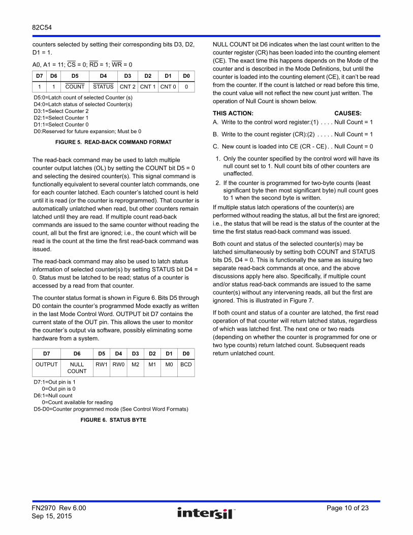
counters selected by setting their corresponding bits D3, D2, D1 = 1.
The read-back command may be used to latch multiple counter output latches (OL) by setting the COUNT bit D5 = 0 and selecting the desired counter(s). This signal command is functionally equivalent to several counter latch commands, one for each counter latched. Each counter’s latched count is held until it is read (or the counter is reprogrammed). That counter is automatically unlatched when read, but other counters remain latched until they are read. If multiple count read-back commands are issued to the same counter without reading the count, all but the first are ignored; i.e., the count which will be read is the count at the time the first read-back command was issued.
The read-back command may also be used to latch status information of selected counter(s) by setting STATUS bit D4 = 0. Status must be latched to be read; status of a counter is accessed by a read from that counter.
The counter status format is shown in Figure 6. Bits D5 through D0 contain the counter’s programmed Mode exactly as written in the last Mode Control Word. OUTPUT bit D7 contains the current state of the OUT pin. This allows the user to monitor the counter’s output via software, possibly eliminating some hardware from a system.
NULL COUNT bit D6 indicates when the last count written to the counter register (CR) has been loaded into the counting element (CE). The exact time this happens depends on the Mode of the counter and is described in the Mode Definitions, but until the counter is loaded into the counting element (CE), it can’t be read from the counter. If the count is latched or read before this time, the count value will not reflect the new count just written. The operation of Null Count is shown below.
THIS ACTION: CAUSES:
A. Write to the control word register:(1) . . . . Null Count = 1
B. Write to the count register (CR):(2) . . . . . Null Count = 1
C. New count is loaded into CE (CR - CE) . . Null Count = 0
1. Only the counter specified by the control word will have its null count set to 1. Null count bits of other counters are unaffected.
2. If the counter is programmed for two-byte counts (least significant byte then most significant byte) null count goes to 1 when the second byte is written.
If multiple status latch operations of the counter(s) are performed without reading the status, all but the first are ignored; i.e., the status that will be read is the status of the counter at the time the first status read-back command was issued.
Both count and status of the selected counter(s) may be latched simultaneously by setting both COUNT and STATUS bits D5, D4 = 0. This is functionally the same as issuing two separate read-back commands at once, and the above discussions apply here also. Specifically, if multiple count and/or status read-back commands are issued to the same counter(s) without any intervening reads, all but the first are ignored. This is illustrated in Figure 7.
If both count and status of a counter are latched, the first read operation of that counter will return latched status, regardless of which was latched first. The next one or two reads (depending on whether the counter is programmed for one or two type counts) return latched count. Subsequent reads return unlatched count.
A0, A1 = 11; CS = 0; RD = 1; WR = 0
D7 D6 D5 D4 D3 D2 D1 D0
1 1 COUNT STATUS CNT 2 CNT 1 CNT 0 0
D5:0=Latch count of selected Counter (s)D4:0=Latch status of selected Counter(s)D3:1=Select Counter 2D2:1=Select Counter 1D1:1=Select Counter 0D0:Reserved for future expansion; Must be 0
FIGURE 5. READ-BACK COMMAND FORMAT
D7 D6 D5 D4 D3 D2 D1 D0
OUTPUT NULL COUNT
RW1 RW0 M2 M1 M0 BCD
D7:1=Out pin is 10=Out pin is 0
D6:1=Null count0=Count available for reading
D5-D0=Counter programmed mode (See Control Word Formats)
FIGURE 6. STATUS BYTE
FN2970 Rev 6.00 Page 10 of 23Sep 15, 2015
82C54
MODE DEFINITIONS
The following are defined for use in describing the operation of the 82C54.
CLK PULSE - A rising edge, then a falling edge, in that order, of a Counter’s CLK input.
TRIGGER - A rising edge of a Counter’s Gate input.
COUNTER LOADING - The transfer of a count from the CR to the CE (See “Functional Description”)
MODE 0: INTERRUPT ON TERMINAL COUNT
Mode 0 is typically used for event counting. After the Control Word is written, OUT is initially low, and will remain low until the Counter reaches zero. OUT then goes high and remains high until a new count or a new Mode 0 Control Word is written to the Counter.
GATE = 1 enables counting; GATE = 0 disables counting. GATE has no effect on OUT.
After the Control Word and initial count are written to a Counter, the initial count will be loaded on the next CLK pulse. This CLK pulse does not decrement the count, so for an initial count of N, OUT does not go high until N + 1 CLK pulses after the initial count is written.
If a new count is written to the Counter it will be loaded on the next CLK pulse and counting will continue from the new count. If a two-byte count is written, the following happens:
1. Writing the first byte disables counting. Out is set low immediately (no clock pulse required).
2. Writing the second byte allows the new count to be loaded on the next CLK pulse.
This allows the counting sequence to be synchronized by software. Again OUT does not go high until N + 1 CLK pulses after the new count of N is written.
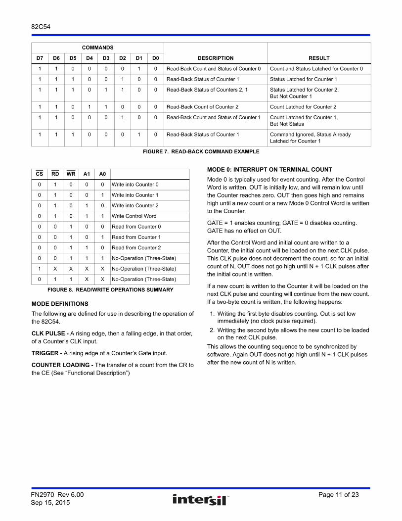
COMMANDS
DESCRIPTION RESULTD7 D6 D5 D4 D3 D2 D1 D0
1 1 0 0 0 0 1 0 Read-Back Count and Status of Counter 0 Count and Status Latched for Counter 0
1 1 1 0 0 1 0 0 Read-Back Status of Counter 1 Status Latched for Counter 1
1 1 1 0 1 1 0 0 Read-Back Status of Counters 2, 1 Status Latched for Counter 2,But Not Counter 1
1 1 0 1 1 0 0 0 Read-Back Count of Counter 2 Count Latched for Counter 2
1 1 0 0 0 1 0 0 Read-Back Count and Status of Counter 1 Count Latched for Counter 1,But Not Status
1 1 1 0 0 0 1 0 Read-Back Status of Counter 1 Command Ignored, Status Already Latched for Counter 1
FIGURE 7. READ-BACK COMMAND EXAMPLE
CS RD WR A1 A0
0 1 0 0 0 Write into Counter 0
0 1 0 0 1 Write into Counter 1
0 1 0 1 0 Write into Counter 2
0 1 0 1 1 Write Control Word
0 0 1 0 0 Read from Counter 0
0 0 1 0 1 Read from Counter 1
0 0 1 1 0 Read from Counter 2
0 0 1 1 1 No-Operation (Three-State)
1 X X X X No-Operation (Three-State)
0 1 1 X X No-Operation (Three-State)
FIGURE 8. READ/WRITE OPERATIONS SUMMARY
FN2970 Rev 6.00 Page 11 of 23Sep 15, 2015
82C54
If an initial count is written while GATE = 0, it will still be loaded on the next CLK pulse. When GATE goes high, OUT will go high N CLK pulses later; no CLK pulse is needed to load the counter as this has already been done.
NOTES: The following conventions apply to all mode timing diagrams.
1. Counters are programmed for binary (not BCD) counting and for reading/writing least significant byte (LSB) only.
2. The counter is always selected (CS always low).
3. CW stands for “Control Word”; CW = 10 means a control word of 10, Hex is written to the counter.
4. LSB stands for Least significant “byte” of count.
5. Numbers below diagrams are count values. The lower number is the least significant byte. The upper number is the most significant byte. Since the counter is programmed to read/write LSB only, the most significant byte cannot be read.
6. N stands for an undefined count.
7. Vertical lines show transitions between count values.
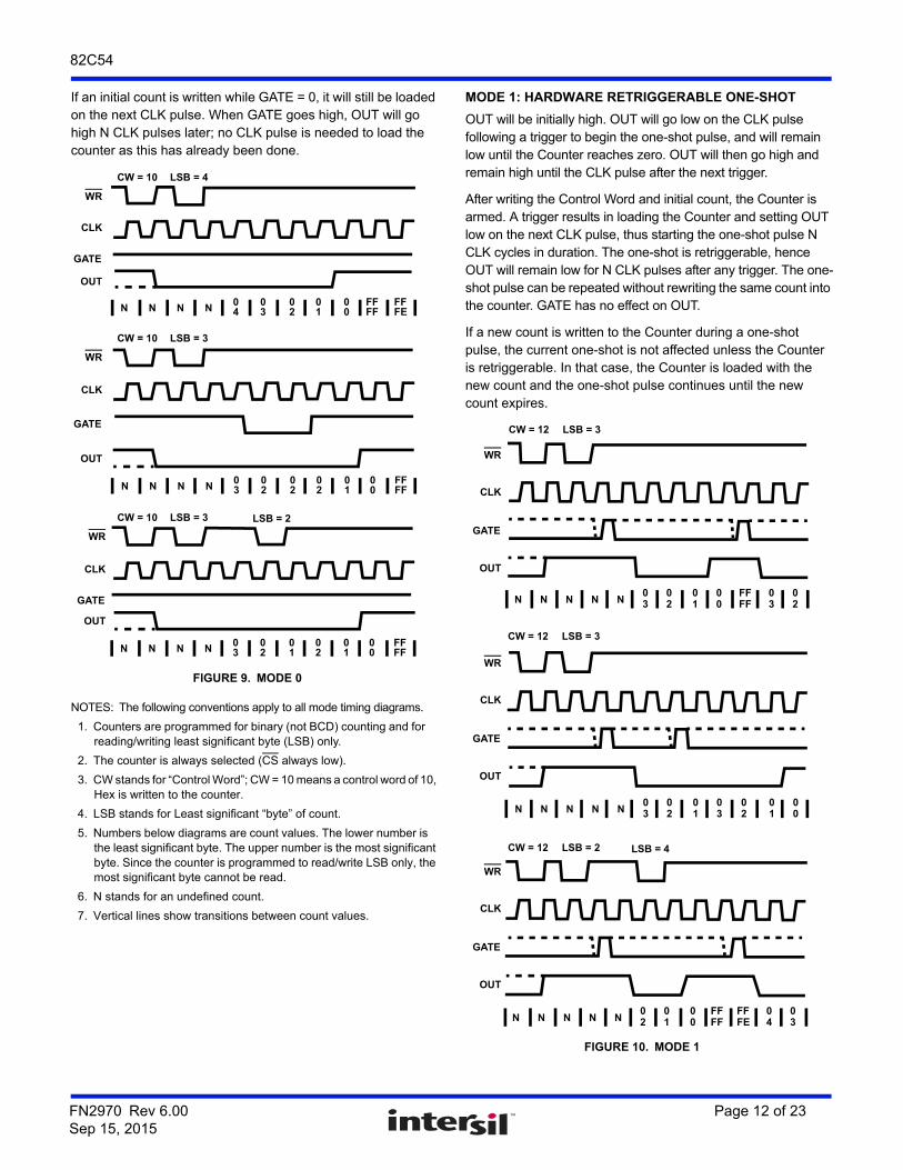
MODE 1: HARDWARE RETRIGGERABLE ONE-SHOT
OUT will be initially high. OUT will go low on the CLK pulse following a trigger to begin the one-shot pulse, and will remain low until the Counter reaches zero. OUT will then go high and remain high until the CLK pulse after the next trigger.
After writing the Control Word and initial count, the Counter is armed. A trigger results in loading the Counter and setting OUT low on the next CLK pulse, thus starting the one-shot pulse N CLK cycles in duration. The one-shot is retriggerable, hence OUT will remain low for N CLK pulses after any trigger. The one-shot pulse can be repeated without rewriting the same count into the counter. GATE has no effect on OUT.
If a new count is written to the Counter during a one-shot pulse, the current one-shot is not affected unless the Counter is retriggerable. In that case, the Counter is loaded with the new count and the one-shot pulse continues until the new count expires.
CW = 10 LSB = 4
WR
CLK
GATE
OUT
WR
CLK
GATE
OUT
WR
CLK
GATE
OUT
CW = 10 LSB = 3
CW = 10 LSB = 3 LSB = 2
N N N N04
03
02
01
00
FFFF
FFFE
N N N N03
02
02
02
01
00
FFFF
N N N N03
02
01
02
01
00
FFFF
FIGURE 9. MODE 0
WR
CLK
GATE
OUT
WR
CLK
GATE
OUT
WR
CLK
GATE
OUT
N N N N03
02
01
00
FFFF
03
02N
CW = 12 LSB = 3
CW = 12 LSB = 3
CW = 12 LSB = 2 LSB = 4
N N N N02
01
00
FFFF
FFFE
04
03N
N N N N03
02
01
03
02
01
00N
FIGURE 10. MODE 1
FN2970 Rev 6.00 Page 12 of 23Sep 15, 2015
82C54
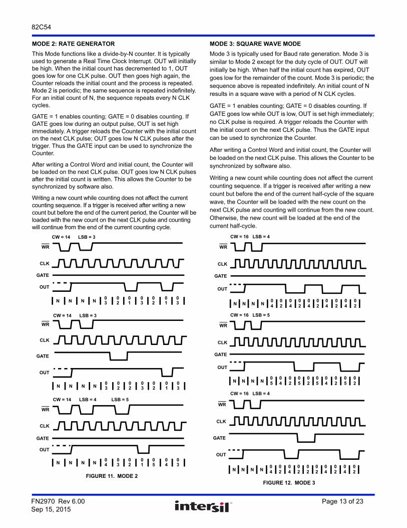
MODE 2: RATE GENERATOR
This Mode functions like a divide-by-N counter. It is typically used to generate a Real Time Clock Interrupt. OUT will initially be high. When the initial count has decremented to 1, OUT goes low for one CLK pulse. OUT then goes high again, the Counter reloads the initial count and the process is repeated. Mode 2 is periodic; the same sequence is repeated indefinitely. For an initial count of N, the sequence repeats every N CLK cycles.
GATE = 1 enables counting; GATE = 0 disables counting. If GATE goes low during an output pulse, OUT is set high immediately. A trigger reloads the Counter with the initial count on the next CLK pulse; OUT goes low N CLK pulses after the trigger. Thus the GATE input can be used to synchronize the Counter.
After writing a Control Word and initial count, the Counter will be loaded on the next CLK pulse. OUT goes low N CLK pulses after the initial count is written. This allows the Counter to be synchronized by software also.
Writing a new count while counting does not affect the current counting sequence. If a trigger is received after writing a new count but before the end of the current period, the Counter will be loaded with the new count on the next CLK pulse and counting will continue from the end of the current counting cycle.
MODE 3: SQUARE WAVE MODE
Mode 3 is typically used for Baud rate generation. Mode 3 is similar to Mode 2 except for the duty cycle of OUT. OUT will initially be high. When half the initial count has expired, OUT goes low for the remainder of the count. Mode 3 is periodic; the sequence above is repeated indefinitely. An initial count of N results in a square wave with a period of N CLK cycles.
GATE = 1 enables counting; GATE = 0 disables counting. If GATE goes low while OUT is low, OUT is set high immediately; no CLK pulse is required. A trigger reloads the Counter with the initial count on the next CLK pulse. Thus the GATE input can be used to synchronize the Counter.
After writing a Control Word and initial count, the Counter will be loaded on the next CLK pulse. This allows the Counter to be synchronized by software also.
Writing a new count while counting does not affect the current counting sequence. If a trigger is received after writing a new count but before the end of the current half-cycle of the square wave, the Counter will be loaded with the new count on the next CLK pulse and counting will continue from the new count. Otherwise, the new count will be loaded at the end of the current half-cycle.
N N N N02
01
03
02
01
03
03
N N N N02
02
03
02
01
03
03
N N N N03
02
01
05
04
03
04
WR
CLK
GATE
OUT
CW = 14 LSB = 3
WR
CLK
GATE
OUT
CW = 14 LSB = 3
WR
CLK
GATE
OUT
CW = 14 LSB = 4 LSB = 5
FIGURE 11. MODE 2
N N N N02
04
02
04
02
04
02
04
04
02
N N N N04
02
05
02
05
04
02
05
05
02
N N N N02
04
02
02
02
04
02
04
04
02
WR
CLK
GATE
OUT
CW = 16 LSB = 4
WR
CLK
GATE
OUT
WR
CLK
GATE
OUT
CW = 16 LSB = 5
CW = 16 LSB = 4
FIGURE 12. MODE 3
FN2970 Rev 6.00 Page 13 of 23Sep 15, 2015
82C54
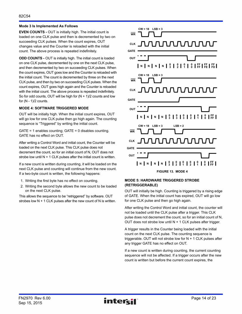
Mode 3 Is Implemented As Follows
EVEN COUNTS - OUT is initially high. The initial count is loaded on one CLK pulse and then is decremented by two on succeeding CLK pulses. When the count expires, OUT changes value and the Counter is reloaded with the initial count. The above process is repeated indefinitely.
ODD COUNTS - OUT is initially high. The initial count is loaded on one CLK pulse, decremented by one on the next CLK pulse, and then decremented by two on succeeding CLK pulses. When the count expires, OUT goes low and the Counter is reloaded with the initial count. The count is decremented by three on the next CLK pulse, and then by two on succeeding CLK pulses. When the count expires, OUT goes high again and the Counter is reloaded with the initial count. The above process is repeated indefinitely. So for odd counts, OUT will be high for (N + 1)/2 counts and low for (N - 1)/2 counts.
MODE 4: SOFTWARE TRIGGERED MODE
OUT will be initially high. When the initial count expires, OUT will go low for one CLK pulse then go high again. The counting sequence is “Triggered” by writing the initial count.
GATE = 1 enables counting; GATE = 0 disables counting. GATE has no effect on OUT.
After writing a Control Word and initial count, the Counter will be loaded on the next CLK pulse. This CLK pulse does not decrement the count, so for an initial count of N, OUT does not strobe low until N + 1 CLK pulses after the initial count is written.
If a new count is written during counting, it will be loaded on the next CLK pulse and counting will continue from the new count. If a two-byte count is written, the following happens:
1. Writing the first byte has no effect on counting.
2. Writing the second byte allows the new count to be loaded on the next CLK pulse.
This allows the sequence to be “retriggered” by software. OUT strobes low N + 1 CLK pulses after the new count of N is written.
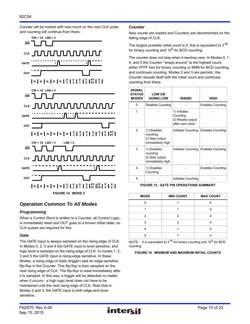
MODE 5: HARDWARE TRIGGERED STROBE (RETRIGGERABLE)
OUT will initially be high. Counting is triggered by a rising edge of GATE. When the initial count has expired, OUT will go low for one CLK pulse and then go high again.
After writing the Control Word and initial count, the counter will not be loaded until the CLK pulse after a trigger. This CLK pulse does not decrement the count, so for an initial count of N, OUT does not strobe low until N + 1 CLK pulses after trigger.
A trigger results in the Counter being loaded with the initial count on the next CLK pulse. The counting sequence is triggerable. OUT will not strobe low for N + 1 CLK pulses after any trigger GATE has no effect on OUT.
If a new count is written during counting, the current counting sequence will not be affected. If a trigger occurs after the new count is written but before the current count expires, the
N N N N02
01
00
FFFF
FFFE
FFFD
03
WR
CLK
GATE
OUT
CW = 18 LSB = 3
WR
CLK
GATE
OUT
WR
CLK
GATE
OUT
CW = 18 LSB = 3
CW = 18 LSB = 3
N N N03
02
01
02
01
00
FFFF
N N N N03
03
02
01
00
FFFF
03
LSB = 2
N
FIGURE 13. MODE 4
FN2970 Rev 6.00 Page 14 of 23Sep 15, 2015
82C54
Counter will be loaded with new count on the next CLK pulse and counting will continue from there.
Operation Common To All Modes
Programming
When a Control Word is written to a Counter, all Control Logic, is immediately reset and OUT goes to a known initial state; no CLK pulses are required for this.
Gate
The GATE input is always sampled on the rising edge of CLK. In Modes 0, 2, 3 and 4 the GATE input is level sensitive, and logic level is sampled on the rising edge of CLK. In modes 1, 2, 3 and 5 the GATE input is rising-edge sensitive. In these Modes, a rising edge of Gate (trigger) sets an edge-sensitive flip-flop in the Counter. This flip-flop is then sampled on the next rising edge of CLK. The flip-flop is reset immediately after it is sampled. In this way, a trigger will be detected no matter when it occurs - a high logic level does not have to be maintained until the next rising edge of CLK. Note that in Modes 2 and 3, the GATE input is both edge-and level-sensitive.
Counter
New counts are loaded and Counters are decremented on the falling edge of CLK.
The largest possible initial count is 0; this is equivalent to 216 for binary counting and 104 for BCD counting.
The counter does not stop when it reaches zero. In Modes 0, 1, 4, and 5 the Counter “wraps around” to the highest count, either FFFF hex for binary counting or 9999 for BCD counting, and continues counting. Modes 2 and 3 are periodic; the Counter reloads itself with the initial count and continues counting from there.N N N N
03
02
01
00
FFFF
03
WR
CLK
GATE
OUT
CW = 1A LSB = 3
N N N N03
02
03
02
01
N N N N03
02
01
00
FFFF
FFFE
WR
CLK
GATE
OUT
CW = 1A LSB = 3
WR
CLK
GATE
OUT
CW = 1A LSB = 3
N
N N00
FFFF
LSB = 5
N05
04
FIGURE 14. MODE 5
SIGNAL STATUS MODES
LOW ORGOING LOW RISING HIGH
0 Disables Counting - Enables Counting
1 - 1) InitiatesCounting2) Resets output after next clock
-
2 1) Disables counting2) Sets output immediately high
Initiates Counting Enables Counting
3 1) Disables counting2) Sets output immediately high
Initiates Counting Enables Counting
4 1) Disables Counting
- Enables Counting
5 - Initiates Counting -
FIGURE 15. GATE PIN OPERATIONS SUMMARY
MODE MIN COUNT MAX COUNT
0 1 0
1 1 0
2 2 0
3 2 0
4 1 0
5 1 0
NOTE: 0 is equivalent to 216 for binary counting and 104 for BCD counting.
FIGURE 16. MINIMUM AND MAXIMUM INITIAL COUNTS
FN2970 Rev 6.00 Page 15 of 23Sep 15, 2015
82C54
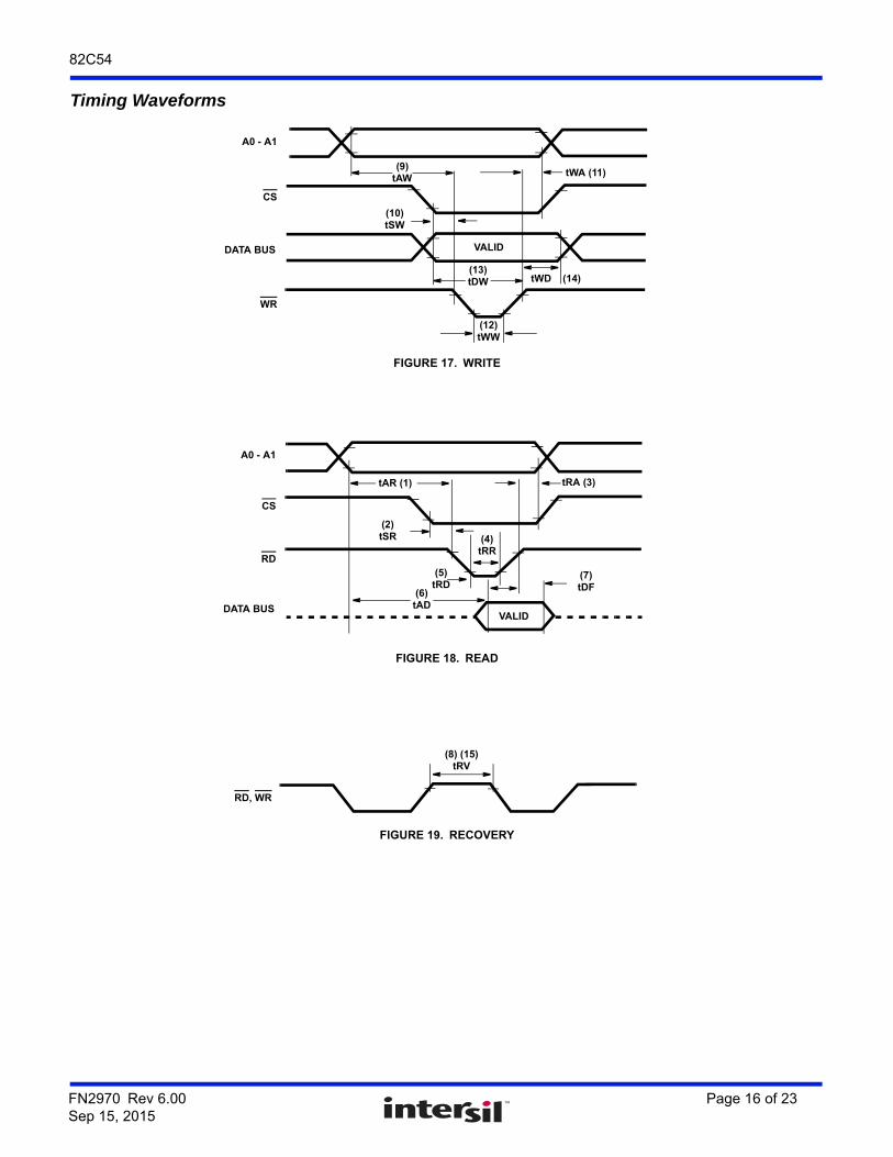
Timing Waveforms
FIGURE 17. WRITE
FIGURE 18. READ
FIGURE 19. RECOVERY
A0 - A1
CS
DATA BUS
WR
(12)tWW
(13)tDW
(10)tSW
(9)tAW
VALID
tWD (14)
tWA (11)
VALID
A0 - A1
CS
RD
DATA BUS
(2)tSR
(6)tAD
(5)tRD
(4)tRR
(7)tDF
tRA (3)tAR (1)
(8) (15)tRV
RD, WR
FN2970 Rev 6.00 Page 16 of 23Sep 15, 2015
82C54
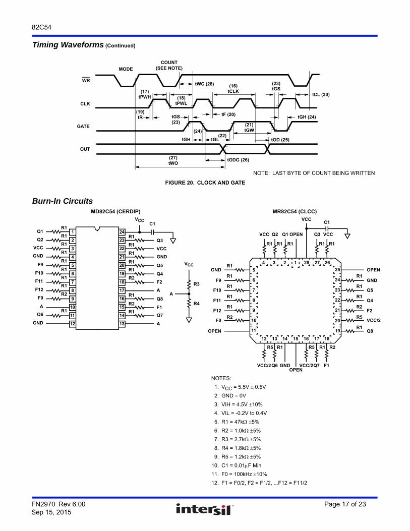
Burn-In CircuitsMD82C54 (CERDIP) MR82C54 (CLCC)
NOTES:
1. VCC = 5.5V 0.5V
2. GND = 0V
3. VIH = 4.5V 10%
4. VIL = -0.2V to 0.4V
5. R1 = 47k 5%
6. R2 = 1.0k 5%
7. R3 = 2.7k 5%
8. R4 = 1.8k 5%
9. R5 = 1.2k 5%
10. C1 = 0.01F Min
11. F0 = 100kHz10%
12. F1 = F0/2, F2 = F1/2, ...F12 = F11/2
FIGURE 20. CLOCK AND GATE
Timing Waveforms (Continued)
WR
CLK
GATE
OUT
MODE
COUNT(SEE NOTE)
(17)tPWH (18)
tPWL
(16)tCLK tGS
(21)tGW
(27)tWO
tGS(23)
tGH
(24)
tGL
tODG (26)
tF (20)
tOD (25)
tGH (24)
NOTE: LAST BYTE OF COUNT BEING WRITTEN
(19)tR
(22)
(23)
tCL (30)
tWC (28)
R1
R1
R1
R1
R1
R1
R1
R1
R2
R1
R1
R1
R1
R1
R2
R1
R1
R2
R1
VCC
GND
Q5
Q4
A
F1
Q7
A
Q3
F2
Q8
Q2
VCC
GND
F9
F11
F0
A
Q6
GND
Q1
F10
F12
VCC
A
1
2
3
4
5
6
7
8
9
10
11
12
16
17
18
19
20
21
22
23
24
15
14
13
VCCC1
R4
R323
24
25
22
21
20
1911
3 2 14
14 15 16 17 1812 13
28 27 26
10
5
6
7
8
9
VCC/2Q6 GNDOPEN
VCC/2 F1Q7
R1
R1
R1
R1
R2
R5
GND
Q5
Q4
Q8
OPEN
F2
VCC/2
R1
R1
R1
R1
R1
R2
F9
F10
F11
OPEN
GND
F12
F0
R5 R1 R5 R1 R2
R1R1R1R1R1
VCC Q2 Q1 OPEN
C1
Q3 VCC
VCC
FN2970 Rev 6.00 Page 17 of 23Sep 15, 2015
82C54
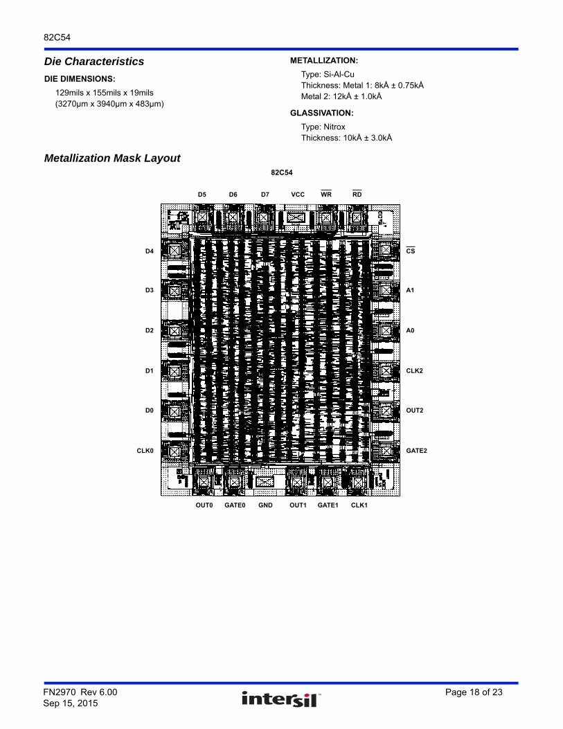
Die Characteristics
DIE DIMENSIONS:
129mils x 155mils x 19mils(3270µm x 3940µm x 483µm)
METALLIZATION:
Type: Si-Al-CuThickness: Metal 1: 8kÅ ± 0.75kÅMetal 2: 12kÅ ± 1.0kÅ
GLASSIVATION:
Type: NitroxThickness: 10kÅ ± 3.0kÅ
Metallization Mask Layout82C54
CS
A1
A0
CLK2
OUT2
GATE2
D4
D3
D2
D1
D0
CLK0
D5 D6 D7 VCC WR RD
OUT0 GATE0 GND OUT1 GATE1 CLK1
FN2970 Rev 6.00 Page 18 of 23Sep 15, 2015

82C54
About IntersilIntersil Corporation is a leading provider of innovative power management and precision analog solutions. The company's products address some of the largest markets within the industrial and infrastructure, mobile computing and high-end consumer markets.
For the most updated datasheet, application notes, related documentation and related parts, please see the respective product information page found at www.intersil.com.
You may report errors or suggestions for improving this datasheet by visiting www.intersil.com/ask.
Reliability reports are also available from our website at www.intersil.com/support.
Revision HistoryThe revision history provided is for informational purposes only and is believed to be accurate, but not warranted. Please go to the web to make sure that you have the latest revision.
DATE REVISION CHANGE
September 15, 2015 FN2970.6 - Updated Ordering Information Table on page 2.- Added Revision History.
FN2970 Rev 6.00 Page 19 of 23Sep 15, 2015
82C54
FN2970 Rev 6.00 Page 20 of 23Sep 15, 2015
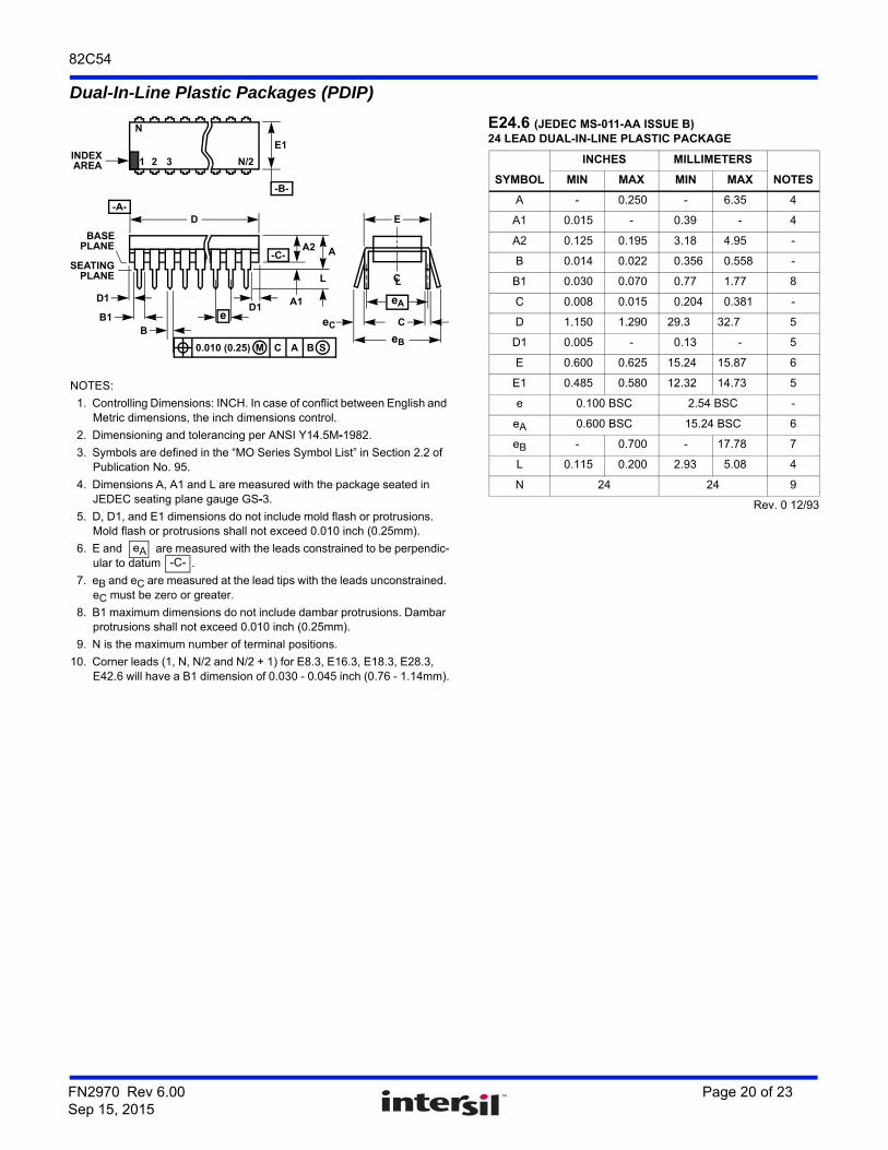
Dual-In-Line Plastic Packages (PDIP)
NOTES:
1. Controlling Dimensions: INCH. In case of conflict between English and Metric dimensions, the inch dimensions control.
2. Dimensioning and tolerancing per ANSI Y14.5M-1982.
3. Symbols are defined in the “MO Series Symbol List” in Section 2.2 of Publication No. 95.
4. Dimensions A, A1 and L are measured with the package seated in JEDEC seating plane gauge GS-3.
5. D, D1, and E1 dimensions do not include mold flash or protrusions. Mold flash or protrusions shall not exceed 0.010 inch (0.25mm).
6. E and are measured with the leads constrained to be perpendic-ular to datum .
7. eB and eC are measured at the lead tips with the leads unconstrained. eC must be zero or greater.
8. B1 maximum dimensions do not include dambar protrusions. Dambar protrusions shall not exceed 0.010 inch (0.25mm).
9. N is the maximum number of terminal positions.
10. Corner leads (1, N, N/2 and N/2 + 1) for E8.3, E16.3, E18.3, E28.3, E42.6 will have a B1 dimension of 0.030 - 0.045 inch (0.76 - 1.14mm).
eA-C-
CL
E
eA
C
eB
eC
-B-
E1INDEX
1 2 3 N/2
N
AREA
SEATING
BASEPLANE
PLANE
-C-
D1
B1B
e
D
D1
AA2
L
A1
-A-
0.010 (0.25) C AM B S
E24.6 (JEDEC MS-011-AA ISSUE B)24 LEAD DUAL-IN-LINE PLASTIC PACKAGE
SYMBOL
INCHES MILLIMETERS
NOTESMIN MAX MIN MAX
A - 0.250 - 6.35 4
A1 0.015 - 0.39 - 4
A2 0.125 0.195 3.18 4.95 -
B 0.014 0.022 0.356 0.558 -
B1 0.030 0.070 0.77 1.77 8
C 0.008 0.015 0.204 0.381 -
D 1.150 1.290 29.3 32.7 5
D1 0.005 - 0.13 - 5
E 0.600 0.625 15.24 15.87 6
E1 0.485 0.580 12.32 14.73 5
e 0.100 BSC 2.54 BSC -
eA 0.600 BSC 15.24 BSC 6
eB - 0.700 - 17.78 7
L 0.115 0.200 2.93 5.08 4
N 24 24 9
Rev. 0 12/93
82C54
FN2970 Rev 6.00 Page 21 of 23Sep 15, 2015
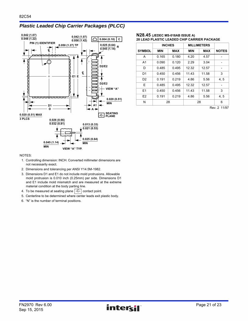
Plastic Leaded Chip Carrier Packages (PLCC)
NOTES:
1. Controlling dimension: INCH. Converted millimeter dimensions are not necessarily exact.
2. Dimensions and tolerancing per ANSI Y14.5M-1982.
3. Dimensions D1 and E1 do not include mold protrusions. Allowable mold protrusion is 0.010 inch (0.25mm) per side. Dimensions D1and E1 include mold mismatch and are measured at the extremematerial condition at the body parting line.
4. To be measured at seating plane contact point.
5. Centerline to be determined where center leads exit plastic body.
6. “N” is the number of terminal positions.
-C-
A1
A
SEATINGPLANE
0.020 (0.51)
MIN
VIEW “A”
D2/E2
0.025 (0.64)0.045 (1.14)
R
0.042 (1.07)0.056 (1.42)
0.050 (1.27) TP
EE1
0.042 (1.07)0.048 (1.22)
PIN (1) IDENTIFIER
CL
D1D
0.020 (0.51) MAX
3 PLCS 0.026 (0.66)0.032 (0.81)
0.045 (1.14)
MIN
0.013 (0.33)
0.021 (0.53)
0.025 (0.64)
MIN
VIEW “A” TYP.
0.004 (0.10) C
-C-
D2/E2
CL
N28.45 (JEDEC MS-018AB ISSUE A)28 LEAD PLASTIC LEADED CHIP CARRIER PACKAGE
SYMBOL
INCHES MILLIMETERS
NOTESMIN MAX MIN MAX
A 0.165 0.180 4.20 4.57 -
A1 0.090 0.120 2.29 3.04 -
D 0.485 0.495 12.32 12.57 -
D1 0.450 0.456 11.43 11.58 3
D2 0.191 0.219 4.86 5.56 4, 5
E 0.485 0.495 12.32 12.57 -
E1 0.450 0.456 11.43 11.58 3
E2 0.191 0.219 4.86 5.56 4, 5
N 28 28 6
Rev. 2 11/97
82C54
FN2970 Rev 6.00 Page 22 of 23Sep 15, 2015
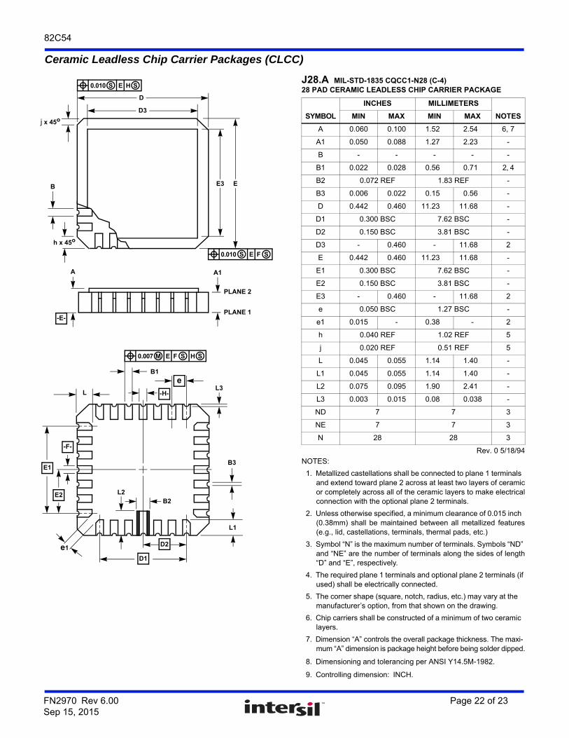
Ceramic Leadless Chip Carrier Packages (CLCC)
D
j x 45o
D3
B
h x 45o
A A1
E
LL3
e
B3
L1
D2
D1
e1
E2
E1
L2
PLANE 2
PLANE 1
E3
B2
0.010 E HS S
0.010 E FS S
-E-
0.007 E FM S H S
B1
-H-
-F-
J28.A MIL-STD-1835 CQCC1-N28 (C-4)28 PAD CERAMIC LEADLESS CHIP CARRIER PACKAGE
SYMBOL
INCHES MILLIMETERS
NOTESMIN MAX MIN MAX
A 0.060 0.100 1.52 2.54 6, 7
A1 0.050 0.088 1.27 2.23 -
B - - - - -
B1 0.022 0.028 0.56 0.71 2, 4
B2 0.072 REF 1.83 REF -
B3 0.006 0.022 0.15 0.56 -
D 0.442 0.460 11.23 11.68 -
D1 0.300 BSC 7.62 BSC -
D2 0.150 BSC 3.81 BSC -
D3 - 0.460 - 11.68 2
E 0.442 0.460 11.23 11.68 -
E1 0.300 BSC 7.62 BSC -
E2 0.150 BSC 3.81 BSC -
E3 - 0.460 - 11.68 2
e 0.050 BSC 1.27 BSC -
e1 0.015 - 0.38 - 2
h 0.040 REF 1.02 REF 5
j 0.020 REF 0.51 REF 5
L 0.045 0.055 1.14 1.40 -
L1 0.045 0.055 1.14 1.40 -
L2 0.075 0.095 1.90 2.41 -
L3 0.003 0.015 0.08 0.038 -
ND 7 7 3
NE 7 7 3
N 28 28 3
Rev. 0 5/18/94
NOTES:
1. Metallized castellations shall be connected to plane 1 terminals and extend toward plane 2 across at least two layers of ceramicor completely across all of the ceramic layers to make electricalconnection with the optional plane 2 terminals.
2. Unless otherwise specified, a minimum clearance of 0.015 inch (0.38mm) shall be maintained between all metallized features(e.g., lid, castellations, terminals, thermal pads, etc.)
3. Symbol “N” is the maximum number of terminals. Symbols “ND” and “NE” are the number of terminals along the sides of length“D” and “E”, respectively.
4. The required plane 1 terminals and optional plane 2 terminals (if used) shall be electrically connected.
5. The corner shape (square, notch, radius, etc.) may vary at the manufacturer’s option, from that shown on the drawing.
6. Chip carriers shall be constructed of a minimum of two ceramic layers.
7. Dimension “A” controls the overall package thickness. The maxi-mum “A” dimension is package height before being solder dipped.
8. Dimensioning and tolerancing per ANSI Y14.5M-1982.
9. Controlling dimension: INCH.
FN2970 Rev 6.00 Page 23 of 23Sep 15, 2015
82C54
Intersil products are manufactured, assembled and tested utilizing ISO9001 quality systems as notedin the quality certifications found at www.intersil.com/en/support/qualandreliability.html
Intersil products are sold by description only. Intersil may modify the circuit design and/or specifications of products at any time without notice, provided that such modification does not, in Intersil's sole judgment, affect the form, fit or function of the product. Accordingly, the reader is cautioned to verify that datasheets are current before placing orders. Information furnished by Intersil is believed to be accurate and reliable. However, no responsibility is assumed by Intersil or its subsidiaries for its use; nor for any infringements of patents or other rights of third parties which may result from its use. No license is granted by implication or otherwise under any patent or patent rights of Intersil or its subsidiaries.
For information regarding Intersil Corporation and its products, see www.intersil.com
For additional products, see www.intersil.com/en/products.html
© Copyright Intersil Americas LLC 1997-2015. All Rights Reserved.All trademarks and registered trademarks are the property of their respective owners.
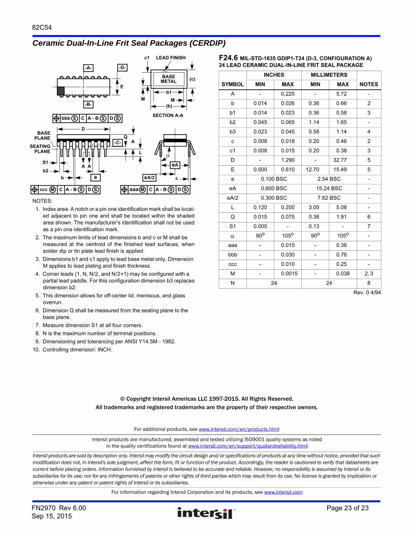
Ceramic Dual-In-Line Frit Seal Packages (CERDIP)
NOTES:
1. Index area: A notch or a pin one identification mark shall be locat-ed adjacent to pin one and shall be located within the shadedarea shown. The manufacturer’s identification shall not be usedas a pin one identification mark.
2. The maximum limits of lead dimensions b and c or M shall be measured at the centroid of the finished lead surfaces, whensolder dip or tin plate lead finish is applied.
3. Dimensions b1 and c1 apply to lead base metal only. Dimension M applies to lead plating and finish thickness.
4. Corner leads (1, N, N/2, and N/2+1) may be configured with a partial lead paddle. For this configuration dimension b3 replacesdimension b2.
5. This dimension allows for off-center lid, meniscus, and glass overrun.
6. Dimension Q shall be measured from the seating plane to the base plane.
7. Measure dimension S1 at all four corners.
8. N is the maximum number of terminal positions.
9. Dimensioning and tolerancing per ANSI Y14.5M - 1982.
10. Controlling dimension: INCH.
bbb C A - BS
c
Q
L
ASEATING
BASE
D
PLANE
PLANE
-D--A-
-C-
-B-
D
E
S1
b2
b
A
e
M
c1
b1
(c)
(b)
SECTION A-A
BASE
LEAD FINISH
METAL
eA/2
A
M
S S
ccc C A - BM DS S aaa C A - BM DS S
eA
F24.6 MIL-STD-1835 GDIP1-T24 (D-3, CONFIGURATION A)24 LEAD CERAMIC DUAL-IN-LINE FRIT SEAL PACKAGE
SYMBOL
INCHES MILLIMETERS
NOTESMIN MAX MIN MAX
A - 0.225 - 5.72 -
b 0.014 0.026 0.36 0.66 2
b1 0.014 0.023 0.36 0.58 3
b2 0.045 0.065 1.14 1.65 -
b3 0.023 0.045 0.58 1.14 4
c 0.008 0.018 0.20 0.46 2
c1 0.008 0.015 0.20 0.38 3
D - 1.290 - 32.77 5
E 0.500 0.610 12.70 15.49 5
e 0.100 BSC 2.54 BSC -
eA 0.600 BSC 15.24 BSC -
eA/2 0.300 BSC 7.62 BSC -
L 0.120 0.200 3.05 5.08 -
Q 0.015 0.075 0.38 1.91 6
S1 0.005 - 0.13 - 7
90o 105o 90o 105o -
aaa - 0.015 - 0.38 -
bbb - 0.030 - 0.76 -
ccc - 0.010 - 0.25 -
M - 0.0015 - 0.038 2, 3
N 24 24 8
Rev. 0 4/94