coupling - uni-due.de · in our directional coupler design between second transmission line and...
TRANSCRIPT
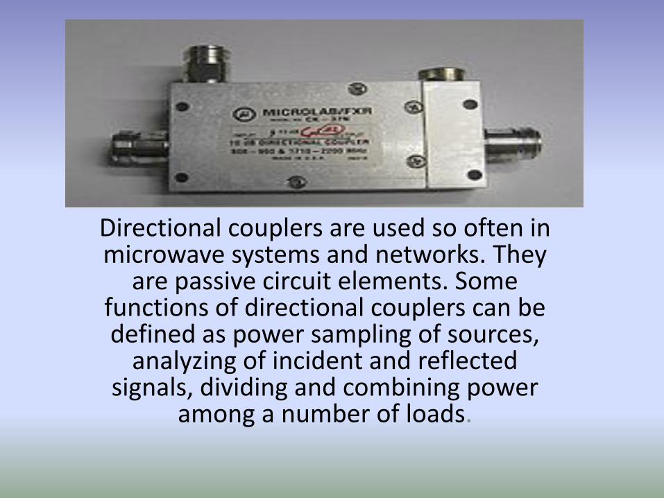
Directional couplers are used so often in microwave systems and networks. They
are passive circuit elements. Some functions of directional couplers can be defined as power sampling of sources, analyzing of incident and reflected
signals, dividing and combining power among a number of loads.
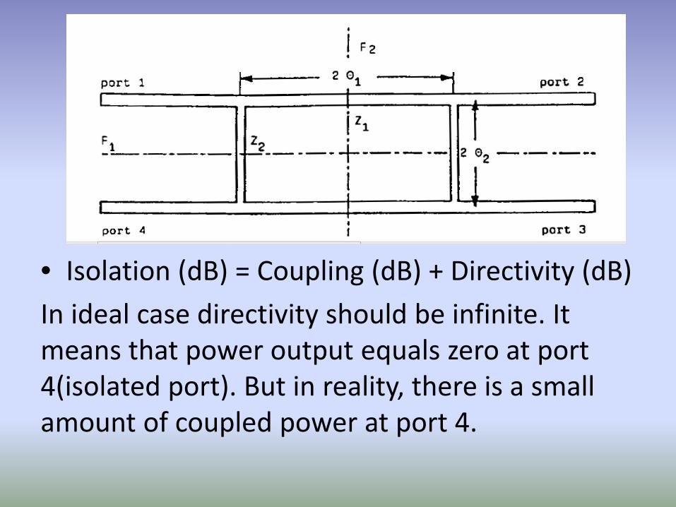
• Isolation (dB) = Coupling (dB) + Directivity (dB)
In ideal case directivity should be infinite. It means that power output equals zero at port 4(isolated port). But in reality, there is a small amount of coupled power at port 4.
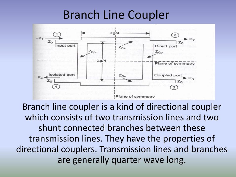
Branch Line Coupler
Branch line coupler is a kind of directional coupler which consists of two transmission lines and two
shunt connected branches between these transmission lines. They have the properties of
directional couplers. Transmission lines and branches are generally quarter wave long.
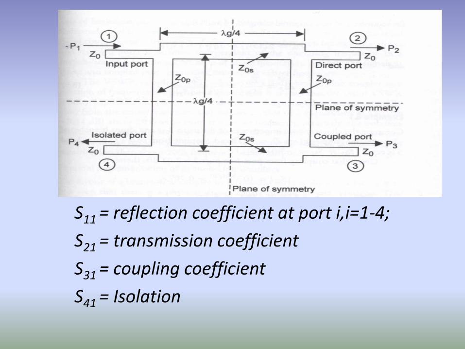
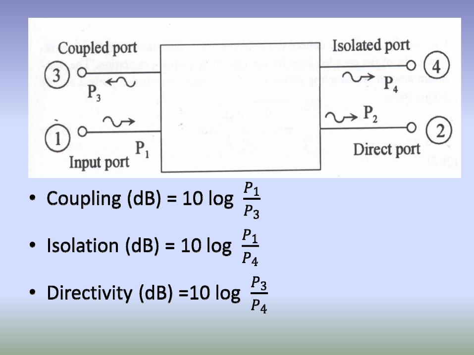
S11 = reflection coefficient at port i,i=1‐4;
S21 = transmission coefficient
S31 = coupling coefficient
S41 = Isolation
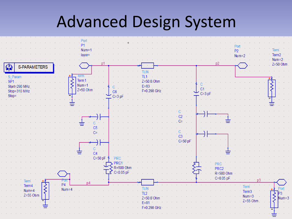
Advanced Design System
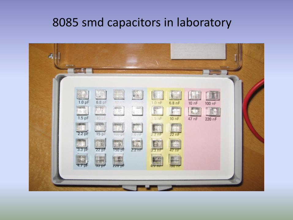
8085 smd capacitors in laboratory
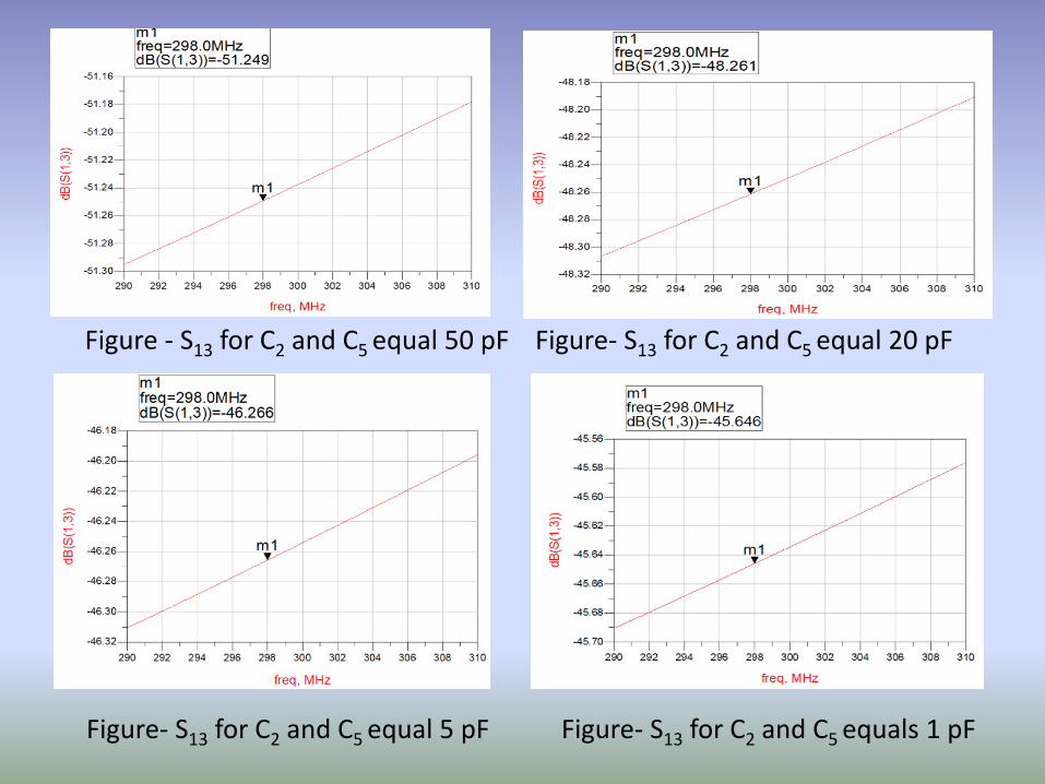
Figure ‐ S13 for C2 and C5 equal 50 pF Figure‐ S13 for C2 and C5 equal 20 pF
Figure‐ S13 for C2 and C5 equal 5 pF Figure‐ S13 for C2 and C5 equals 1 pF
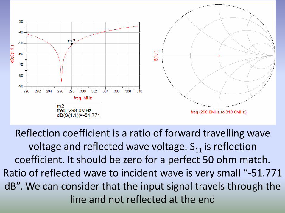
Reflection coefficient is a ratio of forward travelling wave voltage and reflected wave voltage. S11 is reflection
coefficient. It should be zero for a perfect 50 ohm match. Ratio of reflected wave to incident wave is very small “‐51.771 dB”. We can consider that the input signal travels through the
line and not reflected at the end

Figure ‐ S21 transmission coefficient (dB and magnitude)
• As shown in figure, ratio of output voltage to input voltage is nearly ” 0 dB” .The magnitude is “1”.It means that nearly all of the travelling signal passes through and none of that input signal is reflected.

Figure21‐ S41 isolation• S41 is isolation .If all input signal travels through the line, it means that port 4 is isolated from that signal. S41 equals “‐89.264 dB” and less than S31. “ ‐45.646 dB”. It proves that our design works as a directional coupler.
• ‐ 89.264 dB = ‐ 45.646 dB + Directivity(dB) • Directivity = ” ‐43.618 dB”
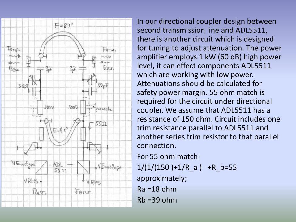
In our directional coupler design between second transmission line and ADL5511, there is another circuit which is designed for tuning to adjust attenuation. The power amplifier employs 1 kW (60 dB) high power level, it can effect components ADL5511 which are working with low power. Attenuations should be calculated for safety power margin. 55 ohm match is required for the circuit under directional coupler. We assume that ADL5511 has a resistance of 150 ohm. Circuit includes one trim resistance parallel to ADL5511 and another series trim resistor to that parallel connection. For 55 ohm match: 1/(1/(150 )+1/R_a ) +R_b=55approximately;Ra =18 ohmRb =39 ohm
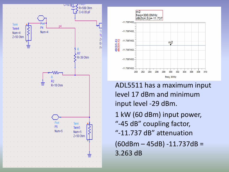
ADL5511 has a maximum input level 17 dBm and minimum input level ‐29 dBm.
1 kW (60 dBm) input power, “‐45 dB” coupling factor, “‐11.737 dB” attenuation
(60dBm – 45dB) ‐11.737dB = 3.263 dB
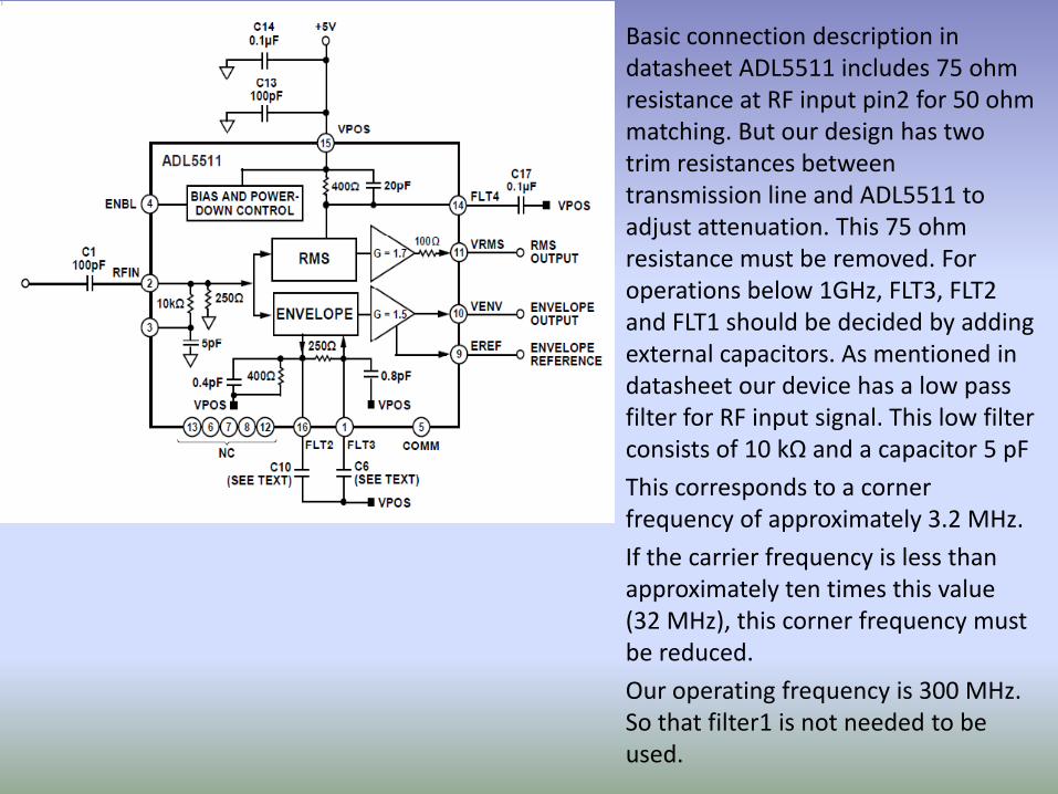
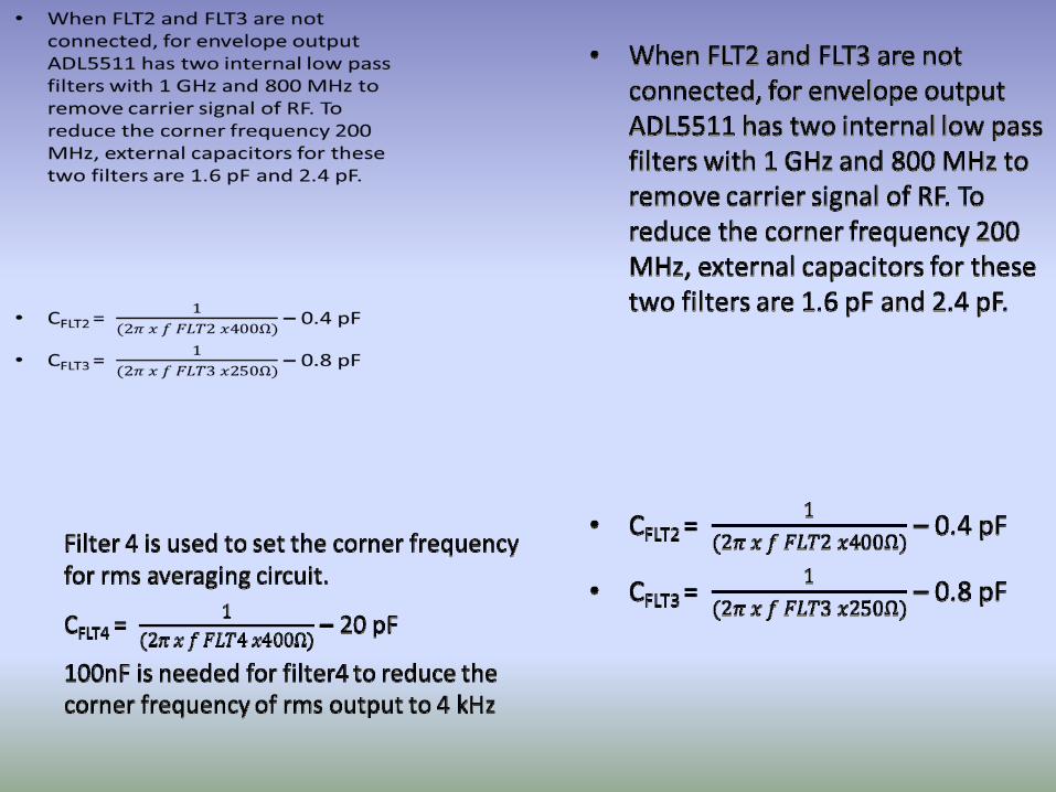
Basic connection description in datasheet ADL5511 includes 75 ohm resistance at RF input pin2 for 50 ohm matching. But our design has two trim resistances between transmission line and ADL5511 to adjust attenuation. This 75 ohm resistance must be removed. For operations below 1GHz, FLT3, FLT2 and FLT1 should be decided by adding external capacitors. As mentioned in datasheet our device has a low pass filter for RF input signal. This low filter consists of 10 kΩ and a capacitor 5 pF
This corresponds to a corner frequency of approximately 3.2 MHz.
If the carrier frequency is less than approximately ten times this value (32 MHz), this corner frequency must be reduced.
Our operating frequency is 300 MHz. So that filter1 is not needed to be used.
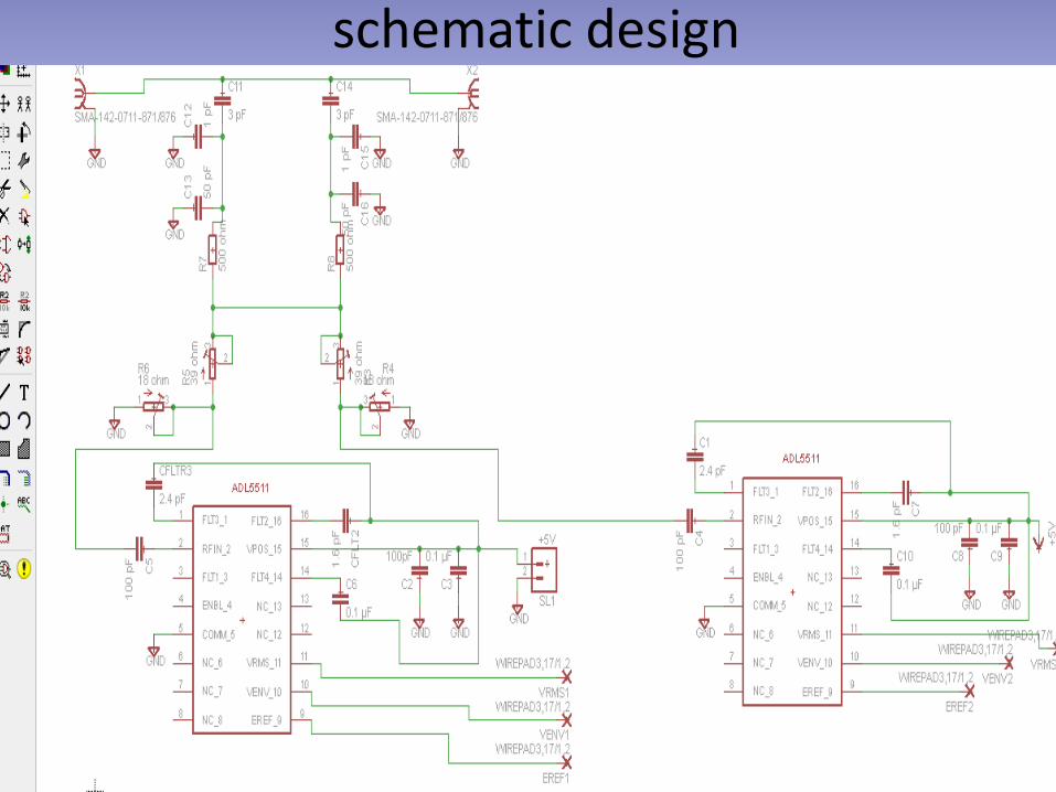
schematic design
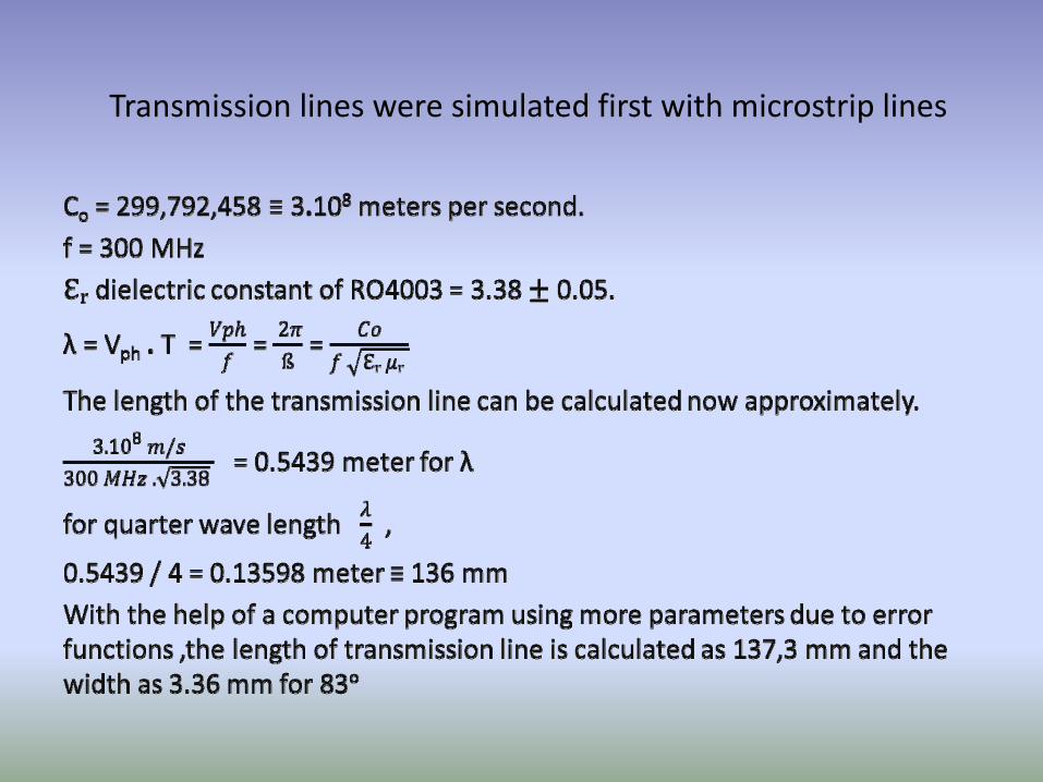
Transmission lines were simulated first with microstrip lines
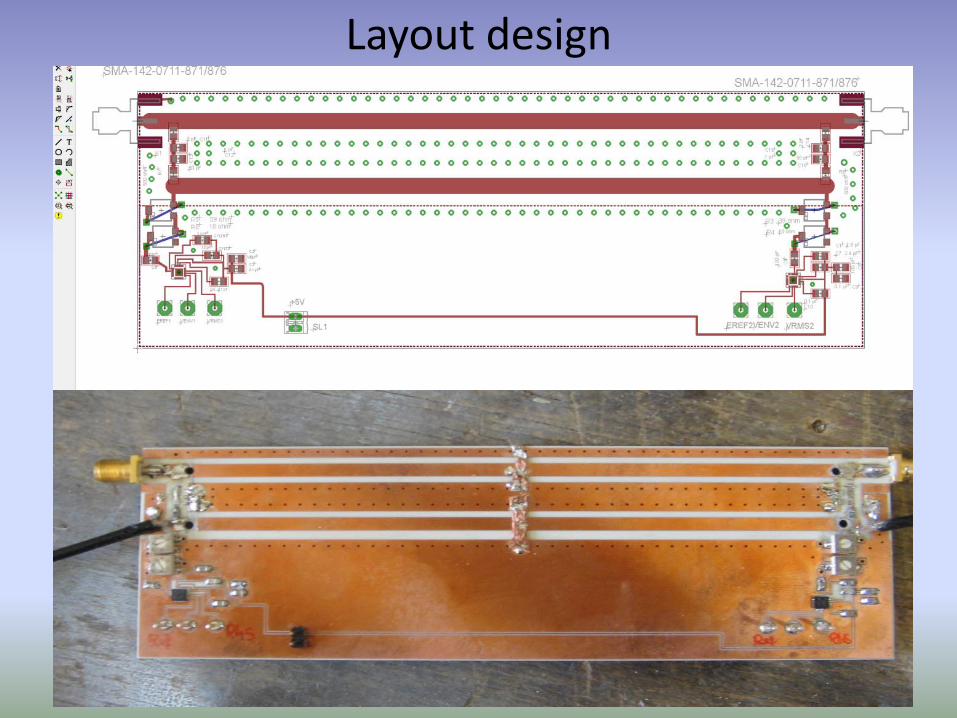
Layout design
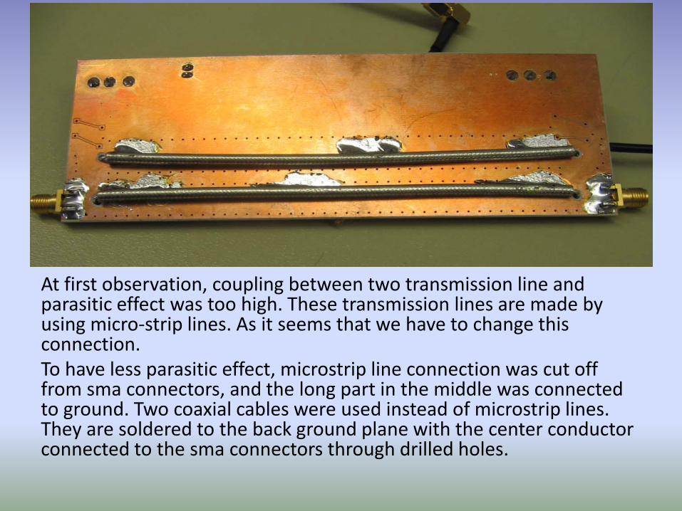
At first observation, coupling between two transmission line and parasitic effect was too high. These transmission lines are made by using micro‐strip lines. As it seems that we have to change this connection. To have less parasitic effect, microstrip line connection was cut off from sma connectors, and the long part in the middle was connected to ground. Two coaxial cables were used instead of microstrip lines. They are soldered to the back ground plane with the center conductor connected to the sma connectors through drilled holes.
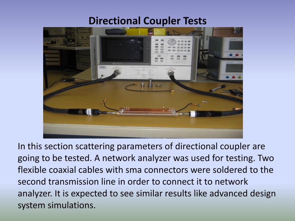
Directional Coupler Tests
In this section scattering parameters of directional coupler are going to be tested. A network analyzer was used for testing. Two flexible coaxial cables with sma connectors were soldered to the second transmission line in order to connect it to network analyzer. It is expected to see similar results like advanced design system simulations.
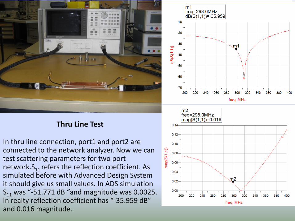
Thru Line Test
In thru line connection, port1 and port2 are connected to the network analyzer. Now we can test scattering parameters for two port network.S11 refers the reflection coefficient. As simulated before with Advanced Design System it should give us small values. In ADS simulation S11 was “‐51.771 dB “and magnitude was 0.0025. In realty reflection coefficient has “‐35.959 dB” and 0.016 magnitude.
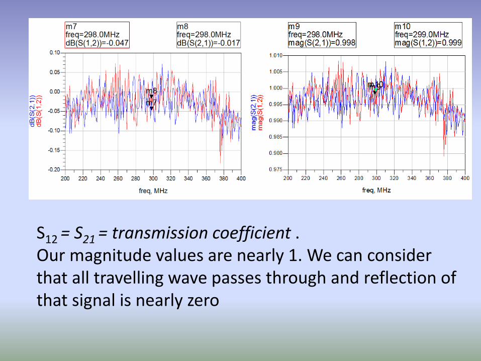
S12 = S21 = transmission coefficient . Our magnitude values are nearly 1. We can consider that all travelling wave passes through and reflection of that signal is nearly zero
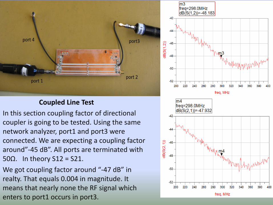
Coupled Line Test
In this section coupling factor of directional coupler is going to be tested. Using the same network analyzer, port1 and port3 were connected. We are expecting a coupling factor around”‐45 dB”. All ports are terminated with 50Ω. In theory S12 = S21.
We got coupling factor around “‐47 dB” in realty. That equals 0.004 in magnitude. It means that nearly none the RF signal which enters to port1 occurs in port3.
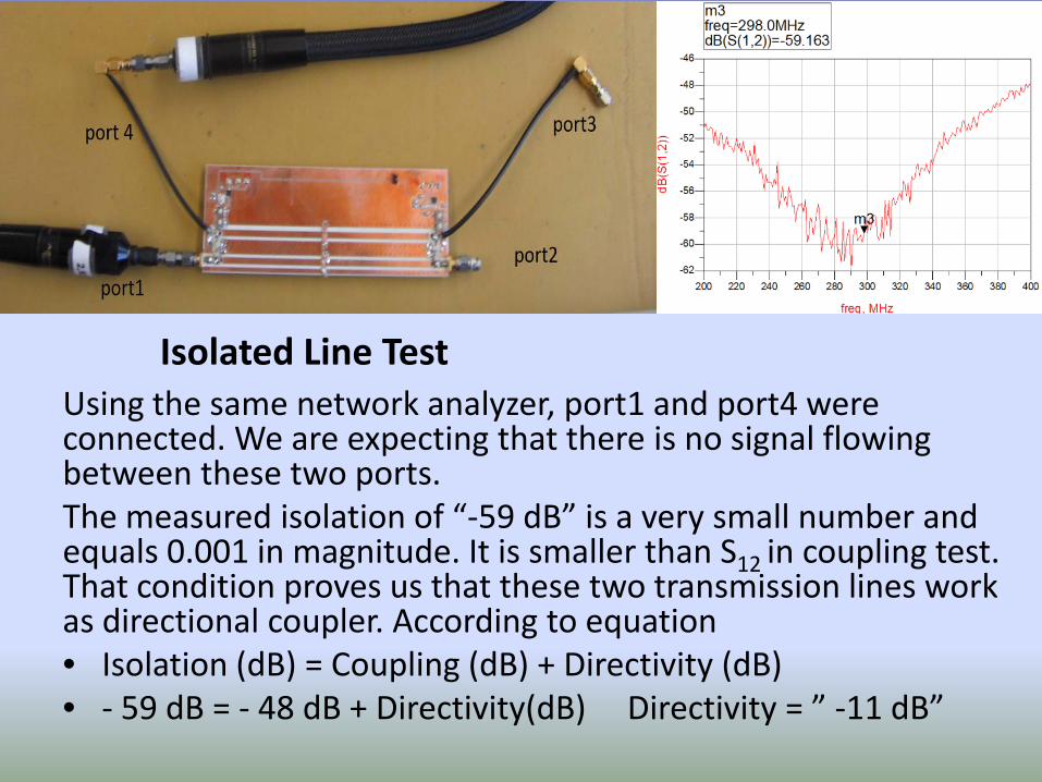
Isolated Line TestUsing the same network analyzer, port1 and port4 were connected. We are expecting that there is no signal flowing between these two ports.The measured isolation of “‐59 dB” is a very small number and equals 0.001 in magnitude. It is smaller than S12 in coupling test. That condition proves us that these two transmission lines work as directional coupler. According to equation • Isolation (dB) = Coupling (dB) + Directivity (dB)• ‐ 59 dB = ‐ 48 dB + Directivity(dB) Directivity = ” ‐11 dB”
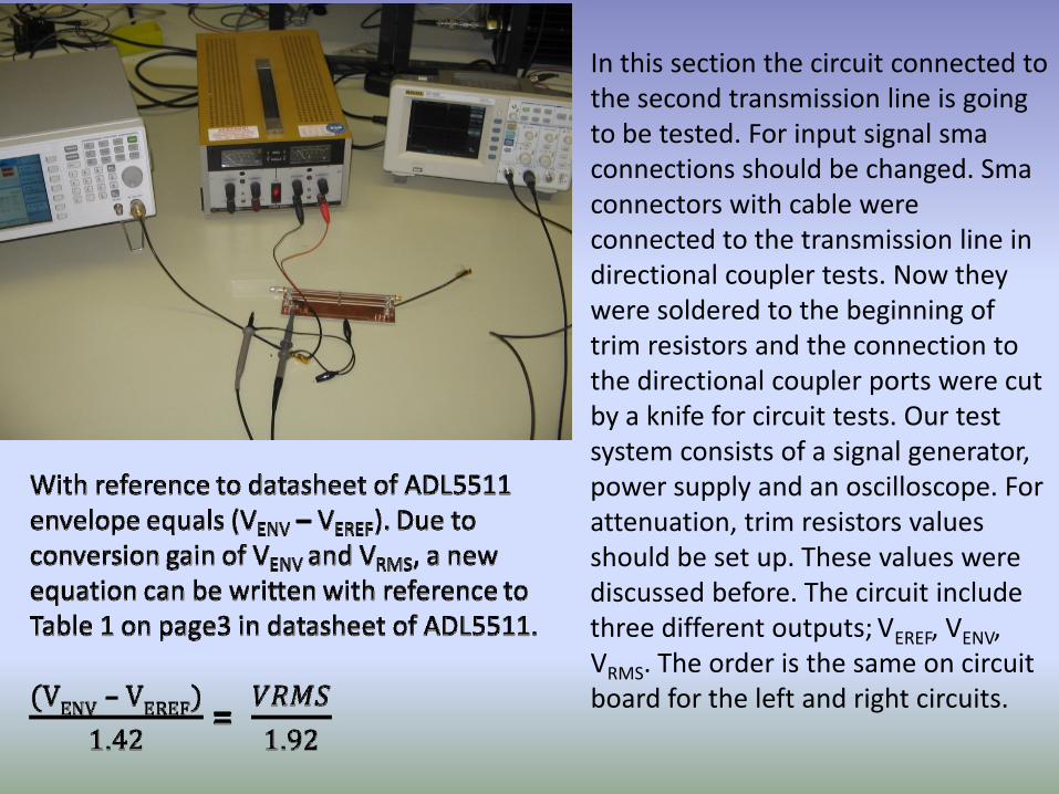
In this section the circuit connected to the second transmission line is going to be tested. For input signal sma connections should be changed. Sma connectors with cable were connected to the transmission line in directional coupler tests. Now they were soldered to the beginning of trim resistors and the connection to the directional coupler ports were cut by a knife for circuit tests. Our test system consists of a signal generator, power supply and an oscilloscope. For attenuation, trim resistors values should be set up. These values were discussed before. The circuit include three different outputs; VEREF, VENV, VRMS. The order is the same on circuit board for the left and right circuits.
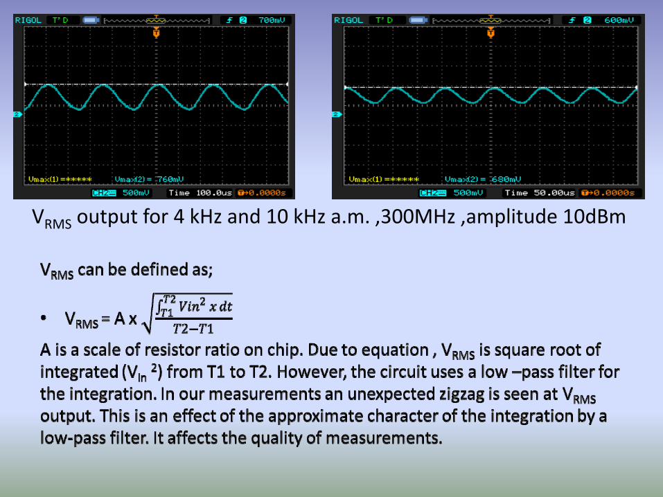
VRMS output for 4 kHz and 10 kHz a.m. ,300MHz ,amplitude 10dBm
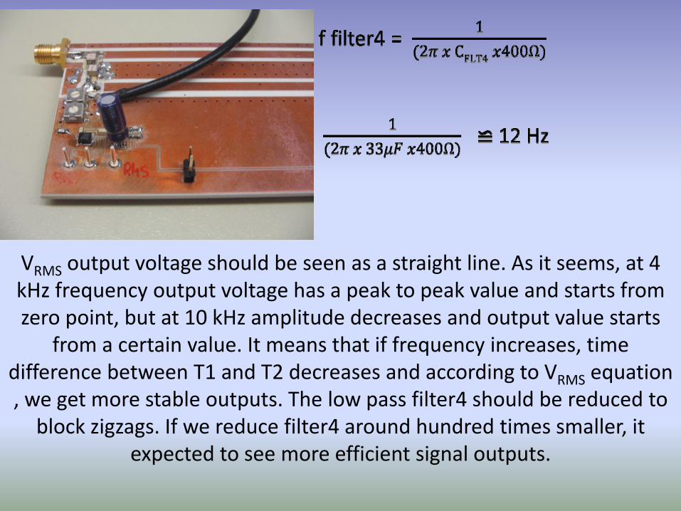
VRMS output voltage should be seen as a straight line. As it seems, at 4 kHz frequency output voltage has a peak to peak value and starts from zero point, but at 10 kHz amplitude decreases and output value starts
from a certain value. It means that if frequency increases, time difference between T1 and T2 decreases and according to VRMS equation , we get more stable outputs. The low pass filter4 should be reduced to block zigzags. If we reduce filter4 around hundred times smaller, it
expected to see more efficient signal outputs.
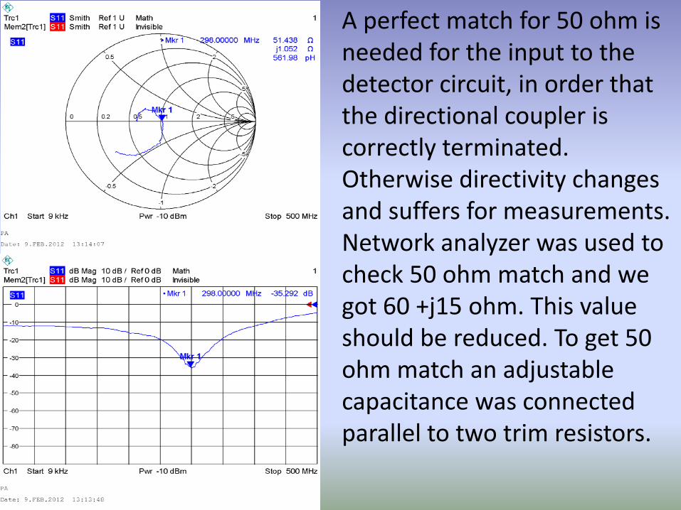
A perfect match for 50 ohm is needed for the input to the detector circuit, in order that the directional coupler is correctly terminated. Otherwise directivity changes and suffers for measurements. Network analyzer was used to check 50 ohm match and we got 60 +j15 ohm. This value should be reduced. To get 50 ohm match an adjustable capacitance was connected parallel to two trim resistors.
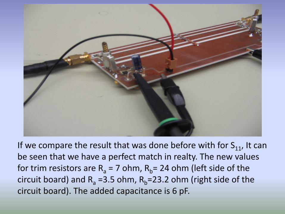
If we compare the result that was done before with for S11, It can be seen that we have a perfect match in realty. The new values for trim resistors are Ra = 7 ohm, Rb= 24 ohm (left side of the circuit board) and Ra =3.5 ohm, Rb=23.2 ohm (right side of the circuit board). The added capacitance is 6 pF.
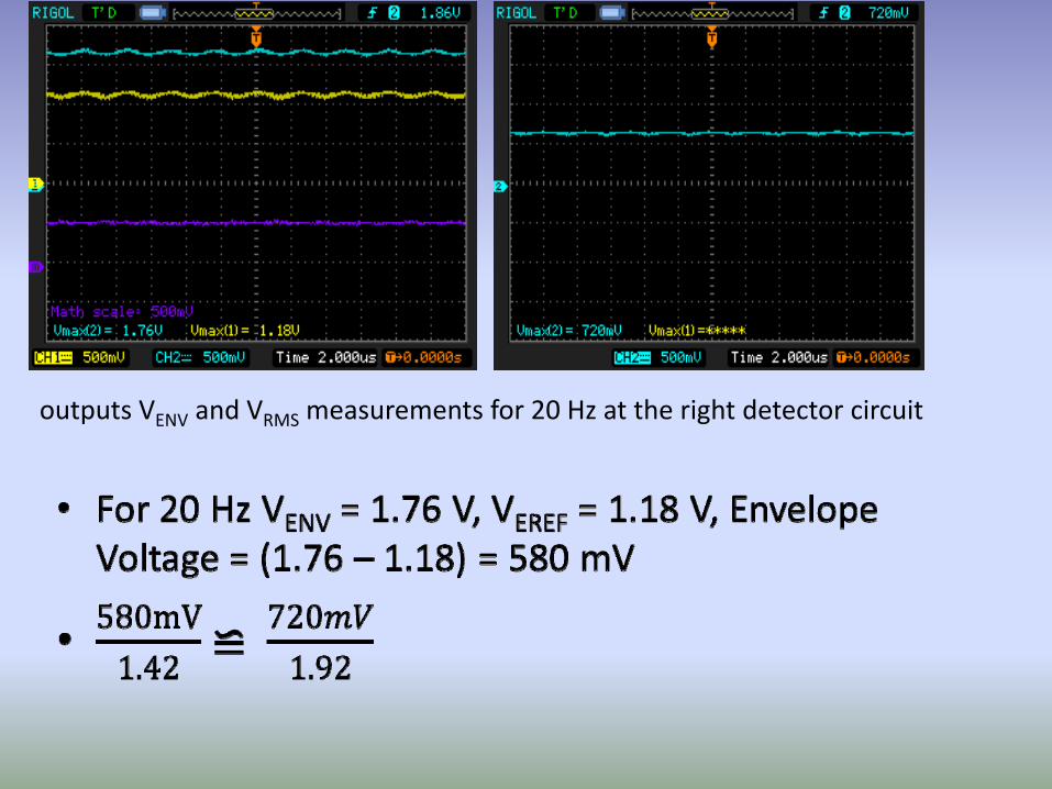
outputs VENV and VRMS measurements for 20 Hz at the right detector circuit
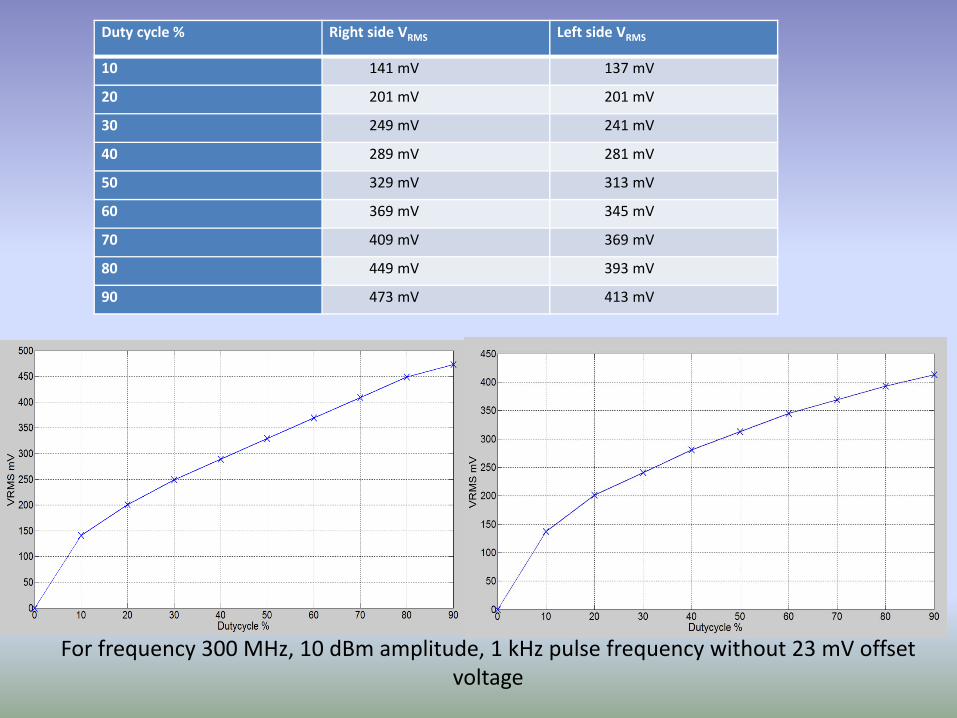
For frequency 300 MHz, 10 dBm amplitude, 1 kHz pulse frequency without 23 mV offset voltage
Duty cycle % Right side VRMS Left side VRMS
10 141 mV 137 mV
20 201 mV 201 mV
30 249 mV 241 mV
40 289 mV 281 mV
50 329 mV 313 mV
60 369 mV 345 mV
70 409 mV 369 mV
80 449 mV 393 mV
90 473 mV 413 mV
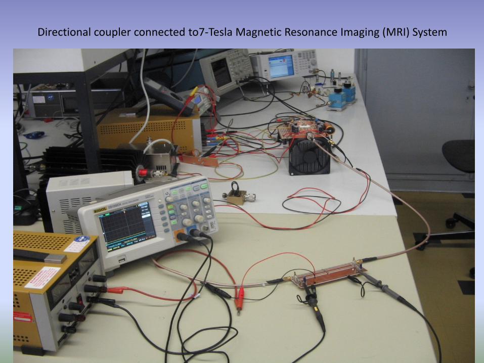
Directional coupler connected to7‐Tesla Magnetic Resonance Imaging (MRI) System
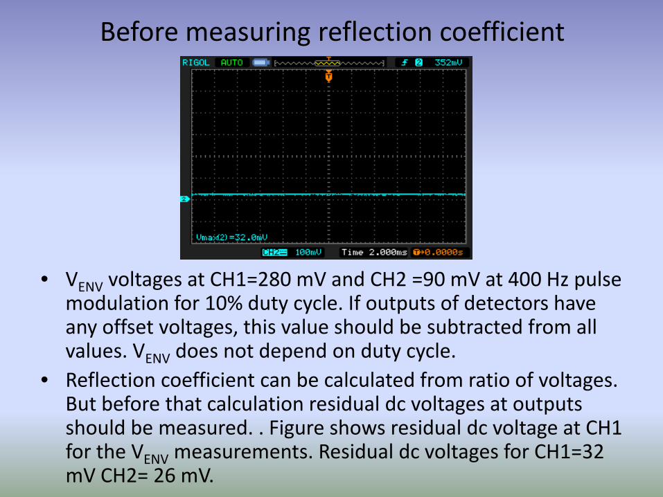
Before measuring reflection coefficient
• VENV voltages at CH1=280 mV and CH2 =90 mV at 400 Hz pulse modulation for 10% duty cycle. If outputs of detectors have any offset voltages, this value should be subtracted from all values. VENV does not depend on duty cycle.
• Reflection coefficient can be calculated from ratio of voltages. But before that calculation residual dc voltages at outputs should be measured. . Figure shows residual dc voltage at CH1 for the VENV measurements. Residual dc voltages for CH1=32 mV CH2= 26 mV.
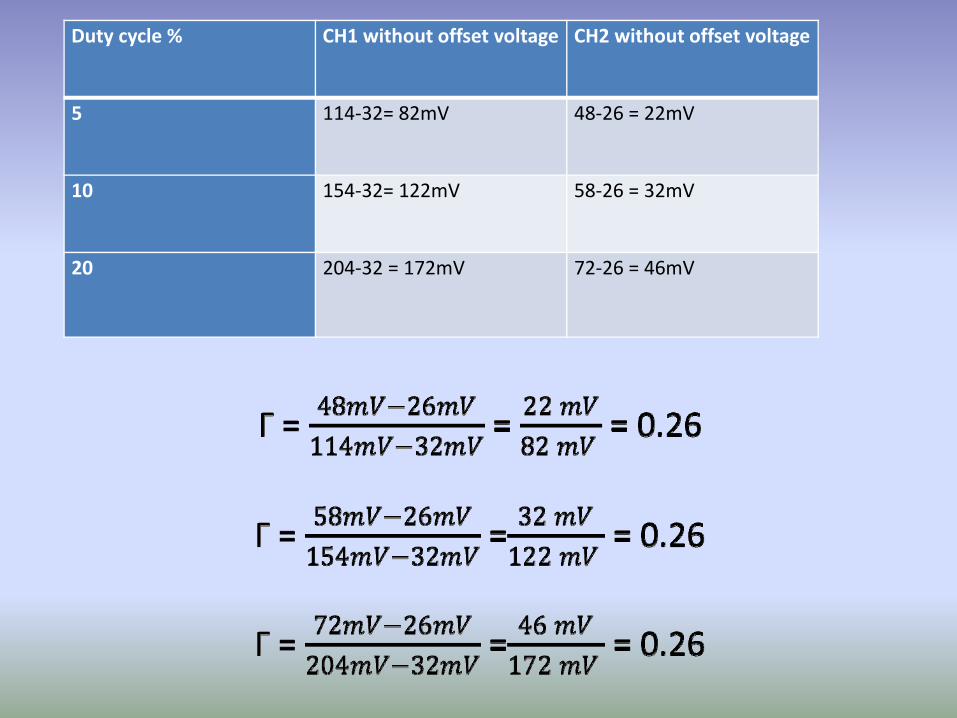
Duty cycle % CH1 without offset voltage CH2 without offset voltage
5 114‐32= 82mV 48‐26 = 22mV
10 154‐32= 122mV 58‐26 = 32mV
20 204‐32 = 172mV 72‐26 = 46mV
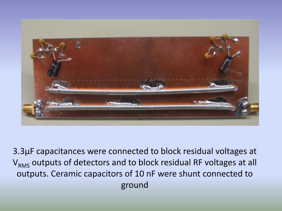
3.3μF capacitances were connected to block residual voltages at VRMS outputs of detectors and to block residual RF voltages at all outputs. Ceramic capacitors of 10 nF were shunt connected to
ground
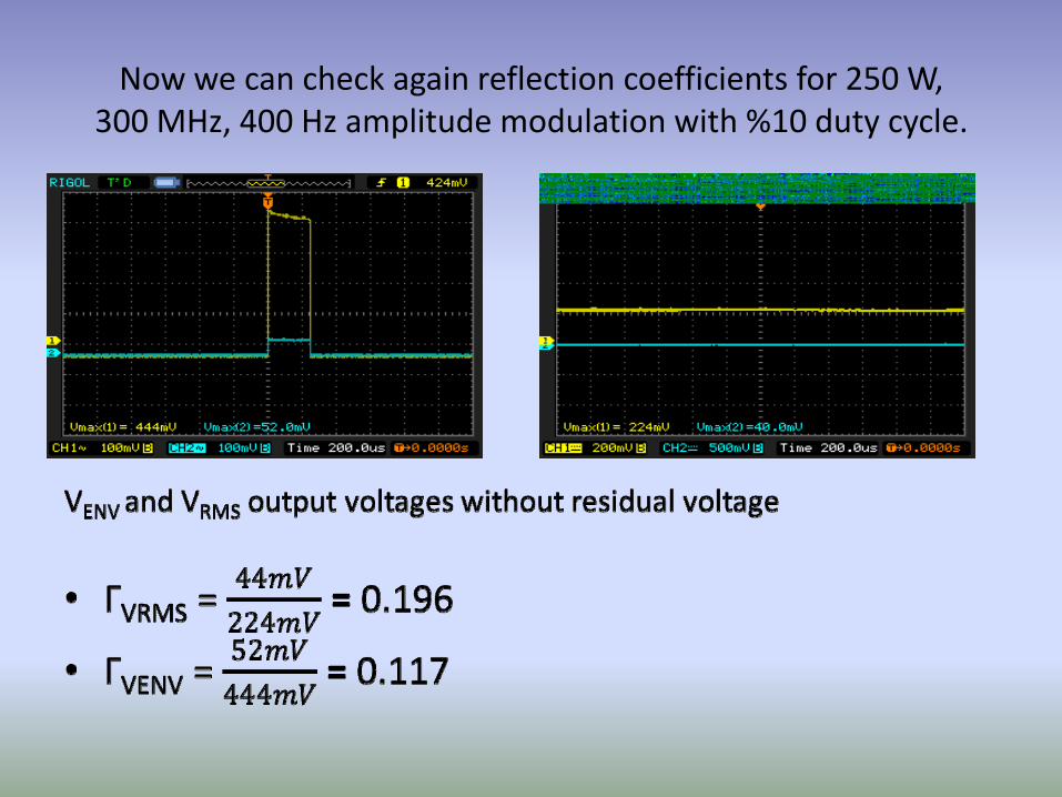
Now we can check again reflection coefficients for 250 W,300 MHz, 400 Hz amplitude modulation with %10 duty cycle.
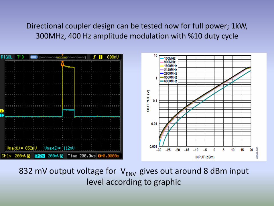
Directional coupler design can be tested now for full power; 1kW, 300MHz, 400 Hz amplitude modulation with %10 duty cycle
832 mV output voltage for VENV gives out around 8 dBm input level according to graphic
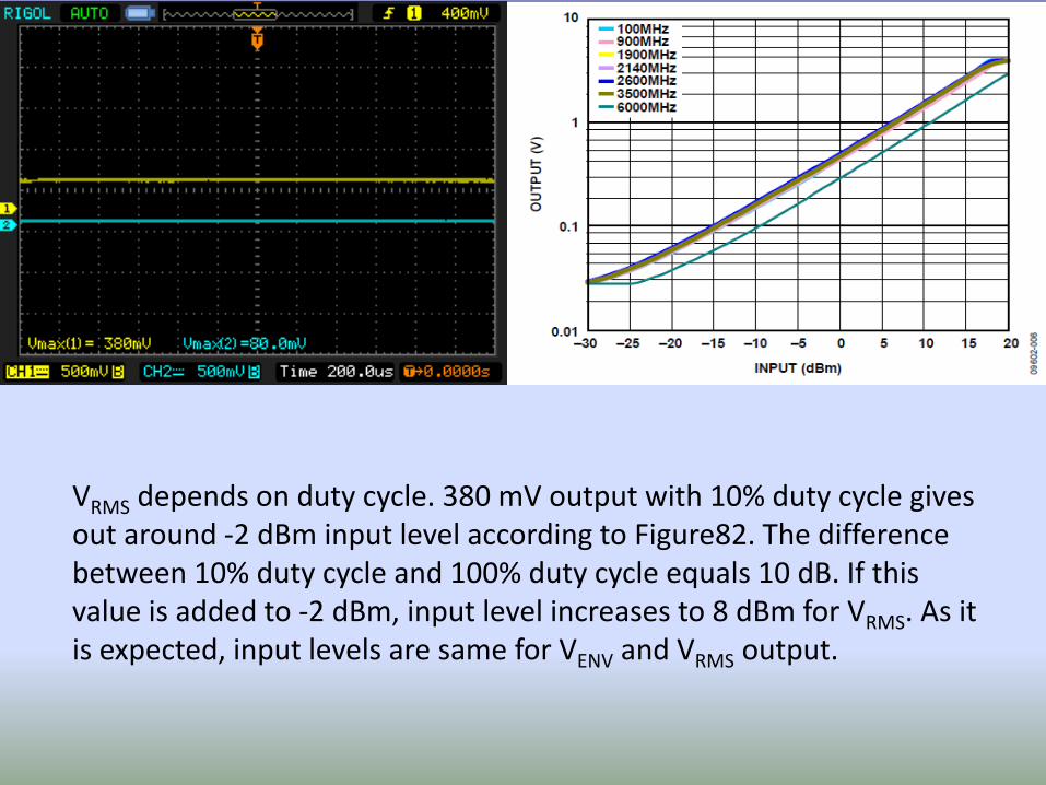
VRMS depends on duty cycle. 380 mV output with 10% duty cycle gives out around ‐2 dBm input level according to Figure82. The difference between 10% duty cycle and 100% duty cycle equals 10 dB. If this value is added to ‐2 dBm, input level increases to 8 dBm for VRMS. As it is expected, input levels are same for VENV and VRMS output.
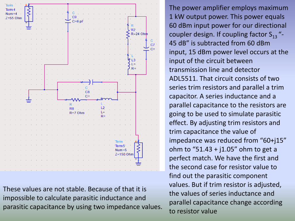
These values are not stable. Because of that it is impossible to calculate parasitic inductance and parasitic capacitance by using two impedance values.
The power amplifier employs maximum 1 kW output power. This power equals 60 dBm input power for our directional coupler design. If coupling factor S13 “‐45 dB” is subtracted from 60 dBminput, 15 dBm power level occurs at the input of the circuit between transmission line and detector ADL5511. That circuit consists of two series trim resistors and parallel a trim capacitor. A series inductance and a parallel capacitance to the resistors are going to be used to simulate parasitic effect. By adjusting trim resistors and trim capacitance the value of impedance was reduced from “60+j15” ohm to “51.43 + j1.05” ohm to get a perfect match. We have the first and the second case for resistor value to find out the parasitic component values. But if trim resistor is adjusted, the values of series inductance and parallel capacitance change according to resistor value
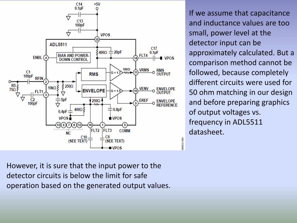
However, it is sure that the input power to the detector circuits is below the limit for safe operation based on the generated output values.
If we assume that capacitance and inductance values are too small, power level at the detector input can be approximately calculated. But a comparison method cannot be followed, because completely different circuits were used for 50 ohm matching in our design and before preparing graphics of output voltages vs. frequency in ADL5511 datasheet.