cortex-m3 reference manual - silicon labs · cortex-m3 reference manual ... the efm32 cortex™ -m3...
TRANSCRIPT

...the world's most energy friendly microcontrollers
2011-02-04 - d0002_Rev1.00 1 www.energymicro.com
Cortex-M3 Reference ManualEFM32 Microcontroller Family
• 32-bit ARM Cortex-M3 processor running up to 32 MHz• Up to 128 KB Flash and 16 KB RAM memory• Energy efficient and fast autonomous peripherals• Ultra low power Energy Modes
The EFM32 microcontroller family revolutionizes the 8- to 32-bit market with acombination of unmatched performance and ultra low power consumption in bothactive- and sleep modes. EFM32 devices only consume 180 µA per MHz in runmode.
EFM32's low energy consumption by far outperforms any other available 8-, 16-,and 32-bit solution. The EFM32 includes autonomous and very energy efficientperipherals, high overall chip- and analog integration, and the performance of theindustry standard 32-bit ARM Cortex-M3 processor.
Innovative and ultra efficient low energy modes with sub µA operation furtherenhance EFM32's ultra low power behaviour and makes the EFM32 microcontrollersperfect for long-lasting battery operated applications.

...the world's most energy friendly microcontrollers
2011-02-04 - d0002_Rev1.00 2 www.energymicro.com
1 Introduction
1.1 About this document
This document provides the information required to use the ARM Cortex-M3 core in EFM32microcontrollers. Further details on the specific implementations within the EFM32 devices can befound in the reference manual and datasheet for the specific device. This document does not provideinformation on debug components, features, or operation.
This material is for microcontroller software and hardware engineers, including those who have noexperience of ARM products.
1.1.1 Typographical conventions
The typographical conventions used in this document are:
italic Highlights important notes, introduces special terminology, denotesinternal cross-references, and citations.
bold Denotes signal names. Also used for terms in descriptive lists, whereappropriate.
< and > Enclose replaceable terms for assembler syntax where they appearin code or code fragments. For example:
LDRSB<cond> <Rt>, [<Rn>, #<offset>]
1.2 About the EFM32 Cortex-M3 processor and core peripherals
The EFM32 Cortex™-M3 processor is a high performance 32-bit processor designed for themicrocontroller market. It offers significant benefits to developers, including:
• outstanding processing performance combined with fast interrupt handling• enhanced system debug with extensive breakpoint and trace capabilities• efficient processor core, system and memories• ultra-low power consumption with integrated sleep modes• platform security, with integrated memory protection unit (MPU). Only available in some devices.

...the world's most energy friendly microcontrollers
2011-02-04 - d0002_Rev1.00 3 www.energymicro.com
Figure 1.1. EFM32 Cortex-M3 implementation
Processorcore
NVIC
Debug Access
Port
Mem oryprotect ion unit
WIC
Serial Wire
viewer
Bus m atrix
Code interface
SRAM and peripheral interface
Data watchpoints
Flashpatch
EFM32 Cortex-M3processor
Em bedded Trace Macrocell
The Cortex-M3 processor is built on a high-performance processor core, with a 3-stage pipeline Harvardarchitecture, making it ideal for demanding embedded applications. The processor delivers exceptionalpower efficiency through an efficient instruction set and extensively optimized design, providing high-end processing hardware including single-cycle 32x32 multiplication and dedicated hardware division.
To facilitate the design of cost-sensitive devices, the Cortex-M3 processor implements tightly-coupledsystem components that reduce processor area while significantly improving interrupt handling andsystem debug capabilities. The Cortex-M3 processor implements a version of the Thumb® instructionset, ensuring high code density and reduced program memory requirements. The Cortex-M3 instructionset provides the exceptional performance expected of a modern 32-bit architecture, with the high codedensity of 8-bit and 16-bit microcontrollers.
The Cortex-M3 processor closely integrates a configurable nested interrupt controller (NVIC), to deliverindustry-leading interrupt performance. The NVIC includes a non-maskable interrupt (NMI), and providesup to 8 interrupt priority levels. The tight integration of the processor core and NVIC provides fastexecution of interrupt service routines (ISRs), dramatically reducing the interrupt latency. This isachieved through the hardware stacking of registers, and the ability to suspend load-multiple and store-multiple operations. Interrupt handlers do not require any assembler stubs, removing any code overheadfrom the ISRs. Tail-chaining optimization also significantly reduces the overhead when switching fromone ISR to another.
To optimize low-power designs, the NVIC integrates with the sleep modes, that include a deep sleepfunction that enables the entire device to be rapidly powered down.
1.2.1 System level interface
The Cortex-M3 processor provides multiple interfaces using AMBA® technology to provide highspeed, low latency memory accesses. It supports unaligned data accesses and implements atomic bitmanipulation that enables faster peripheral controls, system spinlocks and thread-safe Boolean datahandling.

...the world's most energy friendly microcontrollers
2011-02-04 - d0002_Rev1.00 4 www.energymicro.com
The Cortex-M3 processor in some EFM32 devices include a memory protection unit (MPU) that providesfine grain memory control, enabling applications to implement security privilege levels, separating code,data and stack on a task-by-task basis. Such requirements are becoming critical in many embeddedapplications such as automotive. The Memory Protection Unit is only available in some EFM32 devices(Table 1.1 (p. 5) ).
1.2.2 Integrated configurable debug
The Cortex-M3 processor implements a complete hardware debug solution. This provides high systemvisibility of the processor and memory through a 2-pin Serial Wire Debug (SWD) port that is ideal formicrocontrollers and other small package devices.
For system trace the processor integrates an Instrumentation Trace Macrocell (ITM) alongside datawatchpoints and a profiling unit. To enable simple and cost-effective profiling of the system events thesegenerate, a Serial Wire Viewer (SWV) can export a stream of software-generated messages, data trace,and profiling information through a single pin.
The Embedded Trace Macrocell™ (ETM) delivers unrivalled instruction trace capture in an area farsmaller than traditional trace units. The ETM is only available in some EFM32 devices (Table 1.1 (p.5) ).
1.2.3 Cortex-M3 processor features and benefits summary
• tight integration of system peripherals reduces area and development costs• Thumb instruction set combines high code density with 32-bit performance• code-patch ability for ROM system updates• power control optimization of system components• integrated sleep modes for low power consumption• fast code execution permits slower processor clock or increases sleep mode time• hardware division and fast multiplier• deterministic, high-performance interrupt handling for time-critical applications• memory protection unit (MPU) for safety-critical applications. Only available on some devices.• extensive debug and trace capabilities:
• Serial Wire Debug and Serial Wire Trace reduce the number of pins required for debugging andtracing.
1.2.4 Cortex-M3 core peripherals
These are:
Nested Vectored InterruptController
The Nested Vectored Interrupt Controller (NVIC) is an embeddedinterrupt controller that supports low latency interrupt processing.
System control block The System control block (SCB) is the programmers model interfaceto the processor. It provides system implementation information andsystem control, including configuration, control, and reporting ofsystem exceptions.
System timer The system timer, SysTick, is a 24-bit count-down timer. Use thisas a Real Time Operating System (RTOS) tick timer or as a simplecounter.
Memory protection unit The Memory protection unit (MPU) improves system reliability bydefining the memory attributes for different memory regions. Itprovides up to eight different regions, and an optional predefinedbackground region. The Memory Protection Unit is only available insome EFM32 devices (Table 1.1 (p. 5) ).

...the world's most energy friendly microcontrollers
2011-02-04 - d0002_Rev1.00 5 www.energymicro.com
1.2.5 EFM32 Cortex-M3 configurations
The different EFM32 series contain different subsets of peripherals within the ARM Cortex-M3.Table 1.1 (p. 5) shows which features are included in the different EFM32 series.
Table 1.1. Cortex-M3 configuration in EFM32 series
Feature EFM32G EFM32TG EFM32GG
ARM Cortex-M3 version and revision r2p0 r2p1 r2p1
Number of interrupts 30 23 38
Memory Protection Unit (MPU) Yes No Yes
Embedded Trace Macrocell (ETM) No No Yes

...the world's most energy friendly microcontrollers
2011-02-04 - d0002_Rev1.00 6 www.energymicro.com
2 The Cortex-M3 Processor
2.1 Programmers model
This section describes the Cortex-M3 programmers model. In addition to the individual core registerdescriptions, it contains information about the processor modes and privilege levels for softwareexecution and stacks.
2.1.1 Processor mode and privilege levels for software execution
The processor modes are:
Thread mode Used to execute application software. The processor enters Thread mode when itcomes out of reset.
Handler mode Used to handle exceptions. The processor returns to Thread mode when it hasfinished exception processing.
The privilege levels for software execution are:
Unprivileged The software:• has limited access to the MSR and MRS instructions, and cannot use the CPS
instruction• cannot access the system timer, NVIC, or system control block• might have restricted access to memory or peripherals.
Unprivileged software executes at the unprivileged level.Privileged The software can use all the instructions and has access to all resources.
Privileged software executes at the privileged level.
In Thread mode, the CONTROL register controls whether software execution is privileged orunprivileged, see Section 2.1.3.7 (p. 12) . In Handler mode, software execution is always privileged.
Only privileged software can write to the CONTROL register to change the privilege level for softwareexecution in Thread mode. Unprivileged software can use the SVC instruction to make a supervisor callto transfer control to privileged software.
2.1.2 Stacks
The processor uses a full descending stack. This means the stack pointer indicates the last stacked itemon the stack memory. When the processor pushes a new item onto the stack, it decrements the stackpointer and then writes the item to the new memory location. The processor implements two stacks, themain stack and the process stack, with independent copies of the stack pointer, see Section 2.1.3.2 (p.8) .
In Thread mode, the CONTROL register controls whether the processor uses the main stack or theprocess stack, see Section 2.1.3.7 (p. 12) . In Handler mode, the processor always uses the mainstack. The options for processor operations are:
Table 2.1. Summary of processor mode, execution privilege level, and stack use options
Processormode
Used to execute Privilege level for softwareexecution
Stack used
Thread Applications Privileged or unprivileged 1 Main stack or process stack 1

...the world's most energy friendly microcontrollers
2011-02-04 - d0002_Rev1.00 7 www.energymicro.com
Processormode
Used to execute Privilege level for softwareexecution
Stack used
Handler Exception handlers Always privileged Main stack
1See Section 2.1.3.7 (p. 12) .
2.1.3 Core registers
The processor core registers are:
SP (R13)
LR (R14)
PC (R15)
R5
R6
R7
R0
R1
R3
R4
R2
R10
R11
R12
R8
R9
Low registers
High registers
MSP‡PSP‡
PSR
PRIMASK
FAULTMASK
BASEPRI
CONTROL
General-purpose registers
Stack Pointer
Link Register
Program Counter
Program status register
Except ion m ask registers
CONTROL register
Special registers
‡Banked version of SP
Table 2.2. Core register set summary
Name Type 1 Requiredprivilege 2
Reset value Description
R0-R12 RW Either Unknown Section 2.1.3.1 (p. 8)
MSP RW Privileged See description Section 2.1.3.2 (p. 8)
PSP RW Either Unknown Section 2.1.3.2 (p. 8)
LR RW Either 0xFFFFFFFF Section 2.1.3.3 (p. 8)
PC RW Either See description Section 2.1.3.4 (p. 8)
PSR RW Privileged 0x01000000 Section 2.1.3.5 (p. 8)
ASPR RW Either 0x00000000 Section 2.1.3.5.1 (p. 9)
IPSR RO Privileged 0x00000000 Section 2.1.3.5.2 (p. 10)
EPSR RO Privileged 0x01000000 Section 2.1.3.5.3 (p. 10)

...the world's most energy friendly microcontrollers
2011-02-04 - d0002_Rev1.00 8 www.energymicro.com
Name Type 1 Requiredprivilege 2
Reset value Description
PRIMASK RW Privileged 0x00000000 Section 2.1.3.6.1 (p. 11)
FAULTMASK RW Privileged 0x00000000 Section 2.1.3.6.2 (p. 11)
BASEPRI RW Privileged 0x00000000 Section 2.1.3.6.3 (p. 12)
CONTROL RW Privileged 0x00000000 Section 2.1.3.7 (p. 12)
1Describes access type during program execution in thread mode and Handler mode. Debug access can differ.2An entry of Either means privileged and unprivileged software can access the register.
2.1.3.1 General-purpose registers
R0-R12 are 32-bit general-purpose registers for data operations.
2.1.3.2 Stack Pointer
The Stack Pointer (SP) is register R13. In Thread mode, bit[1] of the CONTROL register indicates thestack pointer to use:
• 0 = Main Stack Pointer (MSP). This is the reset value.• 1 = Process Stack Pointer (PSP).
On reset, the processor loads the MSP with the value from address 0x00000000.
2.1.3.3 Link Register
The Link Register (LR) is register R14. It stores the return information for subroutines, function calls,and exceptions. On reset, the processor loads the LR value 0xFFFFFFFF.
2.1.3.4 Program Counter
The Program Counter (PC) is register R15. It contains the current program address. Bit[0] is always 0because instruction fetches must be halfword aligned. On reset, the processor loads the PC with thevalue of the reset vector, which is at address 0x00000004.
2.1.3.5 Program Status Register
The Program Status Register (PSR) combines:
• Application Program Status Register (APSR)• Interrupt Program Status Register (IPSR)• Execution Program Status Register (EPSR).
These registers are mutually exclusive bitfields in the 32-bit PSR. The bit assignments are:
25 24 23
Reserved ISR_NUMBER
31 30 29 28 27
N Z C V
0
ReservedAPSR
IPSR
EPSR Reserved Reserved
26 16 15 10 9
ReservedICI/IT ICI/ITT
Q
8
The PSR bit assignments are:

...the world's most energy friendly microcontrollers
2011-02-04 - d0002_Rev1.00 9 www.energymicro.com
N
31 30 29 28 27 26 25 24 23 16 15 10 9 8 0
Z C V Q ICI/IT T Reserved ICI/IT ISR_NUMBER
Reserved
Access these registers individually or as a combination of any two or all three registers, using the registername as an argument to the MSR or MRS instructions. For example:
• read all of the registers using PSR with the MRS instruction• write to the APSR using APSR with the MSR instruction.
The PSR combinations and attributes are:
Table 2.3. PSR register combinations
Register Type Combination
PSR RW1, 2 APSR, EPSR, and IPSR
IEPSR RO EPSR and IPSR
IAPSR RW1 APSR and IPSR
EAPSR RW2 APSR and EPSR
1The processor ignores writes to the IPSR bits.2Reads of the EPSR bits return zero, and the processor ignores writes to the these bits
See the instruction descriptions Section 3.10.6 (p. 83) and Section 3.10.7 (p. 83) for moreinformation about how to access the program status registers.
2.1.3.5.1 Application Program Status Register
The APSR contains the current state of the condition flags from previous instruction executions. See theregister summary in Table 2.2 (p. 7) for its attributes. The bit assignments are:
Table 2.4. APSR bit assignments
Bits Name Function
[31] N Negative or less than flag:
0 = operation result was positive, zero, greater than, or equal1 = operation result was negative orless than.
[30] Z Zero flag:
0 = operation result was not zero1 = operation result was zero.
[29] C Carry or borrow flag:
0 = add operation did not result in a carry bit or subtract operation resulted in a borrow bit1 = addoperation resulted in a carry bit or subtract operation did not result in a borrow bit.
[28] V Overflow flag:
0 = operation did not result in an overflow1 = operation resulted in an overflow.
[27] Q Sticky saturation flag:
0 = indicates that saturation has not occurred since reset or since the bit was last cleared to zero1= indicates when an SSAT or USAT instruction results in saturation.
This bit is cleared to zero by software using an MRS instruction.
[26:0] - Reserved.

...the world's most energy friendly microcontrollers
2011-02-04 - d0002_Rev1.00 10 www.energymicro.com
2.1.3.5.2 Interrupt Program Status Register
The IPSR contains the exception type number of the current Interrupt Service Routine (ISR). See theregister summary in Table 2.2 (p. 7) for its attributes. The bit assignments are:
Table 2.5. IPSR bit assignments
Bits Name Function
[31:9] - Reserved
[8:0] ISR_NUMBER This is the number of the current exception:
0 = Thread mode
1 = Reserved
2 = NMI
3 = Hard fault
4 = Memory management fault
5 = Bus fault
6 = Usage fault7-10 = Reserved11 = SVCall
12 = Reserved for Debug
13 = Reserved
14 = PendSV
15 = SysTick
16 = IRQ0.
.
.
N = IRQ(N-16). See Table 1.1 (p. 5) for device specificinterrupt number.
see Section 2.3.2 (p. 22) for more information.
2.1.3.5.3 Execution Program Status Register
The EPSR contains the Thumb state bit, and the execution state bits for either the:
• If-Then (IT) instruction• Interruptible-Continuable Instruction (ICI) field for an interrupted load multiple or store multiple
instruction.
See the register summary in Table 2.2 (p. 7) for the EPSR attributes. The bit assignments are:
Table 2.6. EPSR bit assignments
Bits Name Function
[31:27] - Reserved.
[26:25], [15:10] ICI Interruptible-continuable instruction bits, see Section 2.1.3.5.4 (p. 11) .
[26:25], [15:10] IT Indicates the execution state bits of the IT instruction, see Section 3.9.3 (p. 76) .
[24] T Always set to 1.
[23:16] - Reserved.
[9:0] - Reserved.
Attempts to read the EPSR directly through application software using the MSR instruction always returnzero. Attempts to write the EPSR using the MSR instruction in application software are ignored. Fault

...the world's most energy friendly microcontrollers
2011-02-04 - d0002_Rev1.00 11 www.energymicro.com
handlers can examine EPSR value in the stacked PSR to indicate the operation that is at fault. SeeSection 2.3.7 (p. 26)
2.1.3.5.4 Interruptible-continuable instructions
When an interrupt occurs during the execution of an LDM or STM instruction, the processor:
• stops the load multiple or store multiple instruction operation temporarily• stores the next register operand in the multiple operation to EPSR bits[15:12].
After servicing the interrupt, the processor:
• returns to the register pointed to by bits[15:12]• resumes execution of the multiple load or store instruction.
When the EPSR holds ICI execution state, bits[26:25,11:10] are zero.
2.1.3.5.5 If-Then block
The If-Then block contains up to four instructions following a 16-bit IT instruction. Each instruction inthe block is conditional. The conditions for the instructions are either all the same, or some can be theinverse of others. See Section 3.9.3 (p. 76) for more information.
2.1.3.6 Exception mask registers
The exception mask registers disable the handling of exceptions by the processor. Disable exceptionswhere they might impact on timing critical tasks.
To access the exception mask registers use the MSR and MRS instructions, or the CPS instruction tochange the value of PRIMASK or FAULTMASK. See Section 3.10.6 (p. 83) , Section 3.10.7 (p. 83), and Section 3.10.2 (p. 80) for more information.
2.1.3.6.1 Priority Mask Register
The PRIMASK register prevents activation of all exceptions with configurable priority. See the registersummary in Table 2.2 (p. 7) for its attributes. The bit assignments are:
31
Reserved
1 0
PRIMASK
Table 2.7. PRIMASK register bit assignments
Bits Name Function
[31:1] - Reserved
[0] PRIMASK 0 = no effect
1 = prevents the activation of all exceptions with configurable priority.
2.1.3.6.2 Fault Mask Register
The FAULTMASK register prevents activation of all exceptions except for Non-Maskable Interrupt (NMI).See the register summary in Table 2.2 (p. 7) for its attributes. The bit assignments are:

...the world's most energy friendly microcontrollers
2011-02-04 - d0002_Rev1.00 12 www.energymicro.com
Reserved
0131
FAULTMASK
Table 2.8. FAULTMASK register bit assignments
Bits Name Function
[31:1] - Reserved
[0] FAULTMASK 0 = no effect
1 = prevents the activation of all exceptions except for NMI.
The processor clears the FAULTMASK bit to 0 on exit from any exception handler except the NMIhandler.
2.1.3.6.3 Base Priority Mask Register
The BASEPRI register defines the minimum priority for exception processing. When BASEPRI is setto a nonzero value, it prevents the activation of all exceptions with same or lower priority level as theBASEPRI value. See the register summary in Table 2.2 (p. 7) for its attributes. The bit assignmentsare:
BASEPRIReserved
31 078
Table 2.9. BASEPRI register bit assignments
Bits Name Function
[31:8] - Reserved
[7:0] BASEPRI 1 Priority mask bits:
0x0000 = no effectNonzero = defines the base priority for exception processing.
The processor does not process any exception with a priority value greater than or equal toBASEPRI.
1This field is similar to the priority fields in the interrupt priority registers. The processor implements only bits[7:5 of this field,bits[4:0] read as zero and ignore writes. See Section 4.2.7 (p. 92) for more information. Remember that higher priority fieldvalues correspond to lower exception priorities.
2.1.3.7 CONTROL register
The CONTROL register controls the stack used and the privilege level for software execution when theprocessor is in Thread mode. See the register summary in Table 2.2 (p. 7) for its attributes. Thebit assignments are:
31 2 1 0
Reserved
Act ive stack pointerThread m ode privilege level

...the world's most energy friendly microcontrollers
2011-02-04 - d0002_Rev1.00 13 www.energymicro.com
Table 2.10. CONTROL register bit assignments
Bits Name Function
[31:2] - Reserved
[1] Active stack pointer Defines the current stack:
0 = MSP is the current stack pointer
1 = PSP is the current stack pointer.
In Handler mode this bit reads as zero and ignores writes.
[0] Thread mode privilege level Defines the Thread mode privilege level:
0 = privileged1 = unprivileged.
Handler mode always uses the MSP, so the processor ignores explicit writes to the active stack pointerbit of the CONTROL register when in Handler mode. The exception entry and return mechanisms updatethe CONTROL register.
In an OS environment, it is recommended that threads running in Thread mode use the process stackand the kernel and exception handlers use the main stack.
By default, Thread mode uses the MSP. To switch the stack pointer used in Thread mode to the PSP,use the MSR instruction to set the Active stack pointer bit to 1, see Section 3.10.7 (p. 83) .
NoteWhen changing the stack pointer, software must use an ISB instruction immediately afterthe MSR instruction. This ensures that instructions after the ISB execute using the new stackpointer. See Section 3.10.5 (p. 82)
2.1.4 Exceptions and interrupts
The Cortex-M3 processor supports interrupts and system exceptions. The processor and the NestedVectored Interrupt Controller (NVIC) prioritize and handle all exceptions. An exception changes thenormal flow of software control. The processor uses handler mode to handle all exceptions except forreset. See Section 2.3.7.1 (p. 27) and Section 2.3.7.2 (p. 27) for more information.
The NVIC registers control interrupt handling. See Section 4.2 (p. 88) for more information.
2.1.5 Data types
The processor:
• supports the following data types:• 32-bit words• 16-bit halfwords• 8-bit bytes
• supports 64-bit data transfer instructions.• manages all data memory accesses as little-endian. See Section 2.2.1 (p. 15) for more information.
2.1.6 The Cortex Microcontroller Software Interface Standard
For a Cortex-M3 microcontroller system, the Cortex Microcontroller Software Interface Standard(CMSIS) defines:
• a common way to:

...the world's most energy friendly microcontrollers
2011-02-04 - d0002_Rev1.00 14 www.energymicro.com
• access peripheral registers• define exception vectors
• the names of:• the registers of the core peripherals• the core exception vectors
• a device-independent interface for RTOS kernels, including a debug channel.
The CMSIS includes address definitions and data structures for the core peripherals in the Cortex-M3processor. It also includes optional interfaces for middleware components comprising a TCP/IP stackand a Flash file system.
CMSIS simplifies software development by enabling the reuse of template code and the combinationof CMSIS-compliant software components from various middleware vendors. Software vendors canexpand the CMSIS to include their peripheral definitions and access functions for those peripherals.
This document includes the register names defined by the CMSIS, and gives short descriptions of theCMSIS functions that address the processor core and the core peripherals.
NoteThis document uses the register short names defined by the CMSIS. In a few cases thesediffer from the architectural short names that might be used in other documents.
The following sections give more information about the CMSIS:
• Section 2.5.4 (p. 32)• Section 3.2 (p. 37)• Section 4.2.1 (p. 89)• Section 4.2.10.1 (p. 94) .
2.2 Memory model
This section describes the processor memory map, the behavior of memory accesses, and the bit-banding features. The processor has a fixed memory map that provides up to 4GB of addressablememory. The memory map is:

...the world's most energy friendly microcontrollers
2011-02-04 - d0002_Rev1.00 15 www.energymicro.com
Reserved
External device
External RAM
Peripheral
SRAM
Code
0xFFFFFFFF
Private peripheral
bus
0xE01000000xE00FFFFF
0x9FFFFFFF0xA0000000
0x5FFFFFFF0x60000000
0x3FFFFFFF0x40000000
0x1FFFFFFF0x20000000
0x00000000
0x40000000Bit band region
Bit band alias32MB
1MB0x400FFFFF
0x42000000
0x43FFFFFF
Bit band region
Bit band alias32MB
1MB0x20000000
0x200FFFFF
0x22000000
0x23FFFFFF
1.0GB
1.0GB
0.5GB
0.5GB
0.5GB
0xDFFFFFFF0xE0000000
1.0MB
511MB
The regions for SRAM and peripherals include bit-band regions. Bit-banding provides atomic operationsto bit data, see Section 2.2.5 (p. 18) .
The processor reserves regions of the Private peripheral bus (PPB) address range for core peripheralregisters, see Section 4.1 (p. 88) .
2.2.1 Memory regions, types and attributes
The memory map and the programming of the MPU split the memory map into regions. Each region hasa defined memory type, and some regions have additional memory attributes. The memory type andattributes determine the behavior of accesses to the region.
The memory types are:
Normal The processor can re-order transactions for efficiency, or perform speculativereads.

...the world's most energy friendly microcontrollers
2011-02-04 - d0002_Rev1.00 16 www.energymicro.com
Device The processor preserves transaction order relative to other transactions toDevice or Strongly-ordered memory.
Strongly-ordered The processor preserves transaction order relative to all other transactions.
The different ordering requirements for Device and Strongly-ordered memory mean that the memorysystem can buffer a write to Device memory, but must not buffer a write to Strongly-ordered memory.
The additional memory attributes include.
Execute Never (XN) Means the processor prevents instruction accesses. Any attempt to fetch aninstruction from an XN region causes a memory management fault exception.
2.2.2 Memory system ordering of memory accesses
For most memory accesses caused by explicit memory access instructions, the memory system does notguarantee that the order in which the accesses complete matches the program order of the instructions,providing this does not affect the behavior of the instruction sequence. Normally, if correct programexecution depends on two memory accesses completing in program order, software must insert amemory barrier instruction between the memory access instructions, see Section 2.2.4 (p. 17) .
However, the memory system does guarantee some ordering of accesses to Device and Strongly-ordered memory. For two memory access instructions A1 and A2, if A1 occurs before A2 in programorder, the ordering of the memory accesses caused by two instructions is:
Norm al access
Device access, non-shareable
Device access, shareable
Strongly-ordered access
Norm alaccess
Non-shareable Shareable
Strongly-orderedaccess
Device access
A1A2
-
-
-
-
-
<
-
<
-
-
<
<
-
<
<
<
Where:
- Means that the memory system does not guarantee the ordering of the accesses.< Means that accesses are observed in program order, that is, A1 is always observed before A2.
2.2.3 Behavior of memory accesses
The behavior of accesses to each region in the memory map is:
Table 2.11. Memory access behavior
Addressrange
Memory region Memorytype
XN Description
0x00000000-0x1FFFFFFF
Code Normal 1 - Executable region for program code. You can also put data here.
0x20000000-0x3FFFFFFF
SRAM Normal 1 - Executable region for data. You can also put code here.This regionincludes bit band and bit band alias areas, see Table 2.12 (p. 18).
0x40000000-0x5FFFFFFF
Peripheral Device 1 XN 1 This region includes bit band and bit band alias areas, seeTable 2.13 (p. 18) .

...the world's most energy friendly microcontrollers
2011-02-04 - d0002_Rev1.00 17 www.energymicro.com
Addressrange
Memory region Memorytype
XN Description
0x60000000-0x9FFFFFFF
External RAM Normal 1 - Executable region for data.
0xA0000000-0xDFFFFFFF
External device Device 1 XN 1 External Device memory
0xE0000000-0xE00FFFFF
PrivatePeripheral Bus
Strongly-ordered 1
XN 1 This region includes the NVIC, System timer, and system controlblock.
0xE0100000-0xFFFFFFFF
Reserved Device 1 XN 1 Reserved
1See Section 2.2.1 (p. 15) for more information.
The Code, SRAM, and external RAM regions can hold programs. However, ARM recommends thatprograms always use the Code region. This is because the processor has separate buses that enableinstruction fetches and data accesses to occur simultaneously.
The MPU can override the default memory access behavior described in this section. For moreinformation, see Section 4.5 (p. 113) .
2.2.4 Software ordering of memory accesses
The order of instructions in the program flow does not always guarantee the order of the correspondingmemory transactions. This is because:
• the processor can reorder some memory accesses to improve efficiency, providing this does not affectthe behavior of the instruction sequence.
• the processor has multiple bus interfaces• memory or devices in the memory map have different wait states• some memory accesses are buffered or speculative.
Section 2.2.2 (p. 16) describes the cases where the memory system guarantees the order of memoryaccesses. Otherwise, if the order of memory accesses is critical, software must include memory barrierinstructions to force that ordering. The processor provides the following memory barrier instructions:
DMB The Data Memory Barrier (DMB) instruction ensures thatoutstanding memory transactions complete before subsequentmemory transactions. See Section 3.10.3 (p. 81) .
DSB The Data Synchronization Barrier (DSB) instruction ensures thatoutstanding memory transactions complete before subsequentinstructions execute. See Section 3.10.4 (p. 82) .
ISB The Instruction Synchronization Barrier (ISB) ensures that the effectof all completed memory transactions is recognizable by subsequentinstructions. See Section 3.10.5 (p. 82) .
Use memory barrier instructions in, for example:
• MPU programming:• Use a DSB instruction to ensure the effect of the MPU takes place immediately at the end of context
switching.• Use an ISB instruction to ensure the new MPU setting takes effect immediately after programming
the MPU region or regions, if the MPU configuration code was accessed using a branch or call.If the MPU configuration code is entered using exception mechanisms, then an ISB instruction isnot required.
• Vector table. If the program changes an entry in the vector table, and then enables the correspondingexception, use a DMB instruction between the operations. This ensures that if the exception is takenimmediately after being enabled the processor uses the new exception vector.

...the world's most energy friendly microcontrollers
2011-02-04 - d0002_Rev1.00 18 www.energymicro.com
• Self-modifying code. If a program contains self-modifying code, use an ISB instruction immediatelyafter the code modification in the program. This ensures subsequent instruction execution uses theupdated program.
• Memory map switching. If the system contains a memory map switching mechanism, use a DSBinstruction after switching the memory map in the program. This ensures subsequent instructionexecution uses the updated memory map.
• Dynamic exception priority change. When an exception priority has to change when the exception ispending or active, use DSB instructions after the change. This ensures the change takes effect oncompletion of the DSB instruction.
• Using a semaphore in multi-master system. If the system contains more than one bus master, forexample, if another processor is present in the system, each processor must use a DMB instructionafter any semaphore instructions, to ensure other bus masters see the memory transactions in theorder in which they were executed.
Memory accesses to Strongly-ordered memory, such as the system control block, do not require theuse of DMB instructions.
2.2.5 Bit-banding
A bit-band region maps each word in a bit-band alias region to a single bit in the bit-band region. Thebit-band regions occupy the lowest 1MB of the SRAM and peripheral memory regions.
The memory map has two 32MB alias regions that map to two 1MB bit-band regions:
• accesses to the 32MB SRAM alias region map to the 1MB SRAM bit-band region, as shown inTable 2.12 (p. 18)
• accesses to the 32MB peripheral alias region map to the 1MB peripheral bit-band region, as shownin Table 2.13 (p. 18) .
Table 2.12. SRAM memory bit-banding regions
Addressrange
Memory region Instruction and data accesses
0x20000000-
0x200FFFFF
SRAM bit-band region Direct accesses to this memory range behave as SRAM memory accesses, butthis region is also bit addressable through bit-band alias.
0x22000000-
0x23FFFFFF
SRAM bit-band alias Data accesses to this region are remapped to bit band region. A write operationis performed as read-modify-write. Instruction accesses are not remapped.
Table 2.13. Peripheral memory bit-banding regions
Addressrange
Memory region Instruction and data accesses
0x40000000-
0x400FFFFF
Peripheral bit-band region Direct accesses to this memory range behave as peripheral memoryaccesses, but this region is also bit addressable through bit-band alias.
0x42000000-
0x43FFFFFF
Peripheral bit-band alias Data accesses to this region are remapped to bit band region. A writeoperation is performed as read-modify-write. Instruction accesses are notpermitted.
NoteA word access to the SRAM or peripheral bit-band alias regions map to a single bit in theSRAM or peripheral bit-band region.
The following formula shows how the alias region maps onto the bit-band region:

...the world's most energy friendly microcontrollers
2011-02-04 - d0002_Rev1.00 19 www.energymicro.com
bit_word_offset = (byte_offset x 32) + (bit_number x 4)
bit_word_addr = bit_band_base + bit_word_offset
where:
• Bit_word_offset is the position of the target bit in the bit-band memory region.• Bit_word_addr is the address of the word in the alias memory region that maps to the targeted bit.• Bit_band_base is the starting address of the alias region.• Byte_offset is the number of the byte in the bit-band region that contains the targeted bit.• Bit_number is the bit position, 0-7, of the targeted bit.
Figure 2.1 (p. 19) shows examples of bit-band mapping between the SRAM bit-band alias regionand the SRAM bit-band region:
• The alias word at 0x23FFFFE0 maps to bit[0] of the bit-band byte at 0x200FFFFF: 0x23FFFFE0 =0x22000000 + (0xFFFFF*32) + (0*4).
• The alias word at 0x23FFFFFC maps to bit[7] of the bit-band byte at 0x200FFFFF: 0x23FFFFFC =0x22000000 + (0xFFFFF*32) + (7*4).
• The alias word at 0x22000000 maps to bit[0] of the bit-band byte at 0x20000000: 0x22000000 =0x22000000 + (0*32) + (0 *4).
• The alias word at 0x2200001C maps to bit[7] of the bit-band byte at 0x20000000: 0x2200001C =0x22000000+ (0*32) + (7*4).
Figure 2.1. Bit-band mapping
0x23FFFFE4
0x22000004
0x23FFFFE00x23FFFFE80x23FFFFEC0x23FFFFF00x23FFFFF40x23FFFFF80x23FFFFFC
0x220000000x220000140x220000180x2200001C 0x220000080x22000010 0x2200000C
32MB alias region
0
7 0
07
0x200000000x200000010x200000020x20000003
6 5 4 3 2 1 07 6 5 4 3 2 1 7 6 5 4 3 2 1 07 6 5 4 3 2 1
07 6 5 4 3 2 1 6 5 4 3 2 107 6 5 4 3 2 1 07 6 5 4 3 2 1
0x200FFFFC0x200FFFFD0x200FFFFE0x200FFFFF
1MB SRAM bit-band region
2.2.5.1 Directly accessing an alias region
Writing to a word in the alias region updates a single bit in the bit-band region.
Bit[0] of the value written to a word in the alias region determines the value written to the targeted bit inthe bit-band region. Writing a value with bit[0] set to 1 writes a 1 to the bit-band bit, and writing a valuewith bit[0] set to 0 writes a 0 to the bit-band bit.

...the world's most energy friendly microcontrollers
2011-02-04 - d0002_Rev1.00 20 www.energymicro.com
Bits[31:1] of the alias word have no effect on the bit-band bit. Writing 0x01 has the same effect as writing0xFF. Writing 0x00 has the same effect as writing 0x0E.
Reading a word in the alias region:
• 0x00000000 indicates that the targeted bit in the bit-band region is set to zero• 0x00000001 indicates that the targeted bit in the bit-band region is set to 1
2.2.5.2 Directly accessing a bit-band region
Section 2.2.3 (p. 16) describes the behavior of direct byte, halfword, or word accesses to the bit-band regions.
2.2.6 Memory endianness
The processor views memory as a linear collection of bytes numbered in ascending order fromzero. For example, bytes 0-3 hold the first stored word, and bytes 4-7 hold the second stored word.Section 2.2.6.1 (p. 20) describes how words of data are stored in memory.
2.2.6.1 Little-endian format
The EFM32 uses a little-endian format, in which the processor stores the least significant byte of a wordat the lowest-numbered byte, and the most significant byte at the highest-numbered byte. For example:
Mem ory Register
Address A
A+ 1
lsbyte
m sbyte
A+ 2
A+ 3
07
B0B1B3 B2
31 2423 1615 8 7 0
B0
B1
B2
B3
2.2.7 Synchronization primitives
The Cortex-M3 instruction set includes pairs of synchronization primitives. These provide a non-blockingmechanism that a thread or process can use to obtain exclusive access to a memory location. Softwarecan use them to perform a guaranteed read-modify-write memory update sequence, or for a semaphoremechanism.
A pair of synchronization primitives comprises:
A Load-Exclusive instruction Used to read the value of a memory location, requesting exclusiveaccess to that location.
A Store-Exclusive instruction Used to attempt to write to the same memory location, returning astatus bit to a register. If this bit is:0 it indicates that the thread or process gained exclusive access to
the memory, and the write succeeds,1 it indicates that the thread or process did not gain exclusive
access to the memory, and no write is performed,
The pairs of Load-Exclusive and Store-Exclusive instructions are:

...the world's most energy friendly microcontrollers
2011-02-04 - d0002_Rev1.00 21 www.energymicro.com
• the word instructions LDREX and STREX• the halfword instructions LDREXH and STREXH• the byte instructions LDREXB and STREXB.
Software must use a Load-Exclusive instruction with the corresponding Store-Exclusive instruction.
To perform a guaranteed read-modify-write of a memory location, software must:
1. Use a Load-Exclusive instruction to read the value of the location.2. Update the value, as required.3. Use a Store-Exclusive instruction to attempt to write the new value back to the memory location, and
tests the returned status bit. If this bit is:0 The read-modify-write completed successfully,1 No write was performed. This indicates that the value returned at step 1 (p. 21) might be out
of date. The software must retry the read-modify-write sequence,
Software can use the synchronization primitives to implement a semaphores as follows:
1. Use a Load-Exclusive instruction to read from the semaphore address to check whether thesemaphore is free.
2. If the semaphore is free, use a Store-Exclusive to write the claim value to the semaphore address.3. If the returned status bit from step 2 (p. 21) indicates that the Store-Exclusive succeeded then the
software has claimed the semaphore. However, if the Store-Exclusive failed, another process mighthave claimed the semaphore after the software performed step 1 (p. 21) .
The Cortex-M3 includes an exclusive access monitor, that tags the fact that the processor has executeda Load-Exclusive instruction.
The processor removes its exclusive access tag if:
• It executes a CLREX instruction• It executes a Store-Exclusive instruction, regardless of whether the write succeeds.• An exception occurs. This means the processor can resolve semaphore conflicts between different
threads.
For more information about the synchronization primitive instructions, see Section 3.4.8 (p. 54) andSection 3.4.9 (p. 56) .
2.2.8 Programming hints for the synchronization primitives
ANSI C cannot directly generate the exclusive access instructions. Some C compilers provide intrinsicfunctions for generation of these instructions:
Table 2.14. C compiler intrinsic functions for exclusive access instructions
Instruction Intrinsic function
LDREX, LDREXH, orLDREXB
unsigned int __ldrex(volatile void *ptr)
STREX, STREXH, orSTREXB
int __strex(unsigned int val, volatilevoid *ptr)
CLREX void __clrex(void)
The actual exclusive access instruction generated depends on the data type of the pointer passed tothe intrinsic function. For example, the following C code generates the require LDREXB operation:

...the world's most energy friendly microcontrollers
2011-02-04 - d0002_Rev1.00 22 www.energymicro.com
__ldrex((volatile char *) 0xFF);
2.3 Exception model
This section describes the exception model.
2.3.1 Exception states
Each exception is in one of the following states:
Inactive The exception is not active and not pending.Pending The exception is waiting to be serviced by the processor.
An interrupt request from a peripheral or from software can change the stateof the corresponding interrupt to pending.
Active An exception that is being serviced by the processor but has not completed.
NoteAn exception handler can interrupt the execution of anotherexception handler. In this case both exceptions are in the activestate.
Active and pending The exception is being serviced by the processor and there is a pendingexception from the same source.
2.3.2 Exception types
The exception types are:
Reset Reset is invoked on power up or a warm reset. The exception modeltreats reset as a special form of exception. When reset is asserted,the operation of the processor stops, potentially at any point in aninstruction. When reset is deasserted, execution restarts from theaddress provided by the reset entry in the vector table. Executionrestarts as privileged execution in Thread mode.
NMI In the EFM32 devices a NonMaskable Interrupt (NMI) can only betriggered by software. This is the highest priority exception other thanreset. It is permanently enabled and has a fixed priority of -2. NMIscannot be:• masked or prevented from activation by any other exception• preempted by any exception other than Reset.
Hard fault A hard fault is an exception that occurs because of an error duringexception processing, or because an exception cannot be managed byany other exception mechanism. Hard faults have a fixed priority of -1,meaning they have higher priority than any exception with configurablepriority.
Memory management fault A memory management fault is an exception that occurs becauseof a memory protection related fault. The MPU or the fixed memoryprotection constraints determines this fault, for both instruction anddata memory transactions. This fault is used to abort instructionaccesses to Execute Never (XN) memory regions, even if the MPUis disabled.
Bus fault A bus fault is an exception that occurs because of a memory relatedfault for an instruction or data memory transaction. This might be froman error detected on a bus in the memory system.

...the world's most energy friendly microcontrollers
2011-02-04 - d0002_Rev1.00 23 www.energymicro.com
Usage fault A usage fault is an exception that occurs because of a fault related toinstruction execution. This includes:• an undefined instruction• an illegal unaligned access• invalid state on instruction execution• an error on exception return.
The following can cause a usage fault when the core is configured toreport them:• an unaligned address on word and halfword memory access• division by zero.
SVCall A supervisor call (SVC) is an exception that is triggered by theSVC instruction. In an OS environment, applications can use SVCinstructions to access OS kernel functions and device drivers.
PendSV PendSV is an interrupt-driven request for system-level service. In anOS environment, use PendSV for context switching when no otherexception is active.
SysTick A SysTick exception is an exception the system timer generates whenit reaches zero. Software can also generate a SysTick exception. In anOS environment, the processor can use this exception as system tick.
Interrupt (IRQ) A interrupt, or IRQ, is an exception signalled by a peripheral, orgenerated by a software request. All interrupts are asynchronousto instruction execution. In the system, peripherals use interrupts tocommunicate with the processor.
Table 2.15. Properties of the different exception types
Exceptionnumber 1
IRQnumber 1
Exception type Priority Vector address oroffset 2
Activation
1 - Reset -3, the highest 0x00000004 Asynchronous
2 -14 NMI -2 0x00000008 Software only
3 -13 Hard fault -1 0x0000000C -
4 -12 Memorymanagement fault
Configurable 3 0x00000010 Synchronous
5 -11 Bus fault Configurable 3 0x00000014 Synchronous when precise,asynchronous when imprecise
6 -10 Usage fault Configurable 3 0x00000018 Synchronous
7-10 - - - Reserved -
11 -5 SVCall Configurable 3 0x0000002C Synchronous
12-13 - - - Reserved -
14 -2 PendSV Configurable 3 0x00000038 Asynchronous
15 -1 SysTick Configurable 3 0x0000003C Asynchronous
16 andabove
0 andabove
Interrupt (IRQ) Configurable 4 0x00000040 andabove 5
Asynchronous
1To simplify the software layer, the CMSIS only uses IRQ numbers and therefore uses negative values for exceptions other thaninterrupts. The IPSR returns the Exception number, see Section 2.1.3.5.2 (p. 10) .2See Section 2.3.4 (p. 24) for more information.3See Section 4.3.9 (p. 102) .4See Section 4.2.7 (p. 92) .5Increasing in steps of 4.
For an asynchronous exception, other than reset, the processor can execute another instruction betweenwhen the exception is triggered and when the processor enters the exception handler.

...the world's most energy friendly microcontrollers
2011-02-04 - d0002_Rev1.00 24 www.energymicro.com
Privileged software can disable the exceptions that Table 2.15 (p. 23) shows as having configurablepriority, see:
• Section 4.3.10 (p. 103)• Section 4.2.3 (p. 90) .
For more information about hard faults, memory management faults, bus faults, and usage faults, seeSection 2.4 (p. 28) .
2.3.3 Exception handlers
The processor handles exceptions using:
Interrupt Service Routines(ISRs)
Interrupts IRQ0 to IRQ(n-1) (n is given by the number of interruptsfor the device, given by Table 1.1 (p. 5) ) are the exceptions handledby ISRs.
Fault handlers Hard fault, memory management fault, usage fault, bus fault are faultexceptions handled by the fault handlers.
System handlers NMI, PendSV, SVCall SysTick, and the fault exceptions are allsystem exceptions that are handled by system handlers.
2.3.4 Vector table
The vector table contains the reset value of the stack pointer, and the start addresses, also calledexception vectors, for all exception handlers. Figure 2.2 (p. 25) shows the order of the exceptionvectors in the vector table. The least-significant bit of each vector must be 1, indicating that the exceptionhandler is Thumb code. The parameter n denotes the number of interrupts for the device, given byTable 1.1 (p. 5) .

...the world's most energy friendly microcontrollers
2011-02-04 - d0002_Rev1.00 25 www.energymicro.com
Figure 2.2. Vector table
Init ial SP value
Reset
Hard fault
NMI
Mem ory m anagem ent fault
Usage fault
Bus fault
0x0000
0x0004
0x0008
0x000C
0x0010
0x0014
0x0018
Reserved
SVCall
PendSV
Reserved for Debug
Syst ick
IRQ0
Reserved
0x002C
0x0038
0x003C
0x0040
OffsetExcept ion num ber
2
3
4
5
6
11
12
14
15
16
18
13
7
10
1
Vector
.
.
.
8
9
IRQ1
IRQ2
0x0044
IRQ(n-1)
170x0048
0x004C
n+ 16
.
.
.
.
.
.
0x040+ 4x(n-1)
IRQ num ber
-14
-13
-12
-11
-10
-5
-2
-1
0
2
1
n-1
On system reset, the vector table is fixed at address 0x00000000. Privileged software can write to theVTOR to relocate the vector table start address to a different memory location, in the range 0x00000080to 0x3FFFFF80, see Section 4.3.5 (p. 98) .
2.3.5 Exception priorities
As Table 2.15 (p. 23) shows, all exceptions have an associated priority, with:
• a lower priority value indicating a higher priority• configurable priorities for all exceptions except Reset, Hard fault, and NMI.
If software does not configure any priorities, then all exceptions with a configurable priority have a priorityof 0. For information about configuring exception priorities see
• Section 4.3.9 (p. 102)• Section 4.2.7 (p. 92) .
NoteConfigurable priority values are in the range 0-7. This means that the Reset, Hard fault, andNMI exceptions, with fixed negative priority values, always have higher priority than anyother exception.

...the world's most energy friendly microcontrollers
2011-02-04 - d0002_Rev1.00 26 www.energymicro.com
For example, assigning a higher priority value to IRQ[0] and a lower priority value to IRQ[1] meansthat IRQ[1] has higher priority than IRQ[0]. If both IRQ[1] and IRQ[0] are asserted, IRQ[1] is processedbefore IRQ[0].
If multiple pending exceptions have the same priority, the pending exception with the lowest exceptionnumber takes precedence. For example, if both IRQ[0] and IRQ[1] are pending and have the samepriority, then IRQ[0] is processed before IRQ[1].
When the processor is executing an exception handler, the exception handler is preempted if a higherpriority exception occurs. If an exception occurs with the same priority as the exception being handled,the handler is not preempted, irrespective of the exception number. However, the status of the newinterrupt changes to pending.
2.3.6 Interrupt priority grouping
To increase priority control in systems with interrupts, the NVIC supports priority grouping. This divideseach interrupt priority register entry into two fields:
• an upper field that defines the group priority• a lower field that defines a subpriority within the group.
Only the group priority determines preemption of interrupt exceptions. When the processor is executingan interrupt exception handler, another interrupt with the same group priority as the interrupt beinghandled does not preempt the handler,
If multiple pending interrupts have the same group priority, the subpriority field determines the order inwhich they are processed. If multiple pending interrupts have the same group priority and subpriority,the interrupt with the lowest IRQ number is processed first.
For information about splitting the interrupt priority fields into group priority and subpriority, seeSection 4.3.6 (p. 99) .
2.3.7 Exception entry and return
Descriptions of exception handling use the following terms:
Preemption When the processor is executing an exception handler, an exception can preemptthe exception handler if its priority is higher than the priority of the exception beinghandled. See Section 2.3.6 (p. 26) for more information about preemption byan interrupt.
When one exception preempts another, the exceptions are called nestedexceptions. See Section 2.3.7.1 (p. 27) more information.
Return This occurs when the exception handler is completed, and:• there is no pending exception with sufficient priority to be serviced• the completed exception handler was not handling a late-arriving exception.
The processor pops the stack and restores the processor state to the state it hadbefore the interrupt occurred. See Section 2.3.7.2 (p. 27) for more information.
Tail-chaining This mechanism speeds up exception servicing. On completion of an exceptionhandler, if there is a pending exception that meets the requirements for exceptionentry, the stack pop is skipped and control transfers to the new exception handler.
Late-arriving This mechanism speeds up preemption. If a higher priority exception occurs duringstate saving for a previous exception, the processor switches to handle the higherpriority exception and initiates the vector fetch for that exception. State saving is notaffected by late arrival because the state saved is the same for both exceptions.Therefore the state saving continues uninterrupted. The processor can accept a latearriving exception until the first instruction of the exception handler of the original

...the world's most energy friendly microcontrollers
2011-02-04 - d0002_Rev1.00 27 www.energymicro.com
exception enters the execute stage of the processor. On return from the exceptionhandler of the late-arriving exception, the normal tail-chaining rules apply.
2.3.7.1 Exception entry
Exception entry occurs when there is a pending exception with sufficient priority and either:
• the processor is in Thread mode• the new exception is of higher priority than the exception being handled, in which case the new
exception preempts the original exception.
When one exception preempts another, the exceptions are nested.
Sufficient priority means the exception has more priority than any limits set by the mask registers, seeSection 2.1.3.6 (p. 11) . An exception with less priority than this is pending but is not handled bythe processor.
When the processor takes an exception, unless the exception is a tail-chained or a late-arrivingexception, the processor pushes information onto the current stack. This operation is referred as stackingand the structure of eight data words is referred as stack frame. The stack frame contains the followinginformation:
• R0-R3, R12• Return address• PSR• LR.
Immediately after stacking, the stack pointer indicates the lowest address in the stack frame. Unlessstack alignment is disabled, the stack frame is aligned to a double-word address. If the STKALIGN bit ofthe Configuration Control Register (CCR) is set to 1, stack align adjustment is performed during stacking.
The stack frame includes the return address. This is the address of the next instruction in the interruptedprogram. This value is restored to the PC at exception return so that the interrupted program resumes.
In parallel to the stacking operation, the processor performs a vector fetch that reads the exceptionhandler start address from the vector table. When stacking is complete, the processor starts executingthe exception handler. At the same time, the processor writes an EXC_RETURN value to the LR.This indicates which stack pointer corresponds to the stack frame and what operation mode the wasprocessor was in before the entry occurred.
If no higher priority exception occurs during exception entry, the processor starts executing the exceptionhandler and automatically changes the status of the corresponding pending interrupt to active.
If another higher priority exception occurs during exception entry, the processor starts executing theexception handler for this exception and does not change the pending status of the earlier exception.This is the late arrival case.
2.3.7.2 Exception return
Exception return occurs when the processor is in Handler mode and executes one of the followinginstructions to load the EXC_RETURN value into the PC:
• a POP instruction that includes the PC• a BX instruction with any register.• an LDR or LDM instruction with the PC as the destination.
EXC_RETURN is the value loaded into the LR on exception entry. The exception mechanism relies onthis value to detect when the processor has completed an exception handler. The lowest four bits of

...the world's most energy friendly microcontrollers
2011-02-04 - d0002_Rev1.00 28 www.energymicro.com
this value provide information on the return stack and processor mode. Table 2.16 (p. 28) shows theEXC_RETURN[3:0] values with a description of the exception return behavior.
The processor sets EXC_RETURN bits[31:4] to 0xFFFFFFF. When this value is loaded into the PCit indicates to the processor that the exception is complete, and the processor initiates the exceptionreturn sequence.
Table 2.16. Exception return behavior
EXC_RETURN[3:0] Description
bXXX0 Reserved.
b0001 Return to Handler mode.
Exception return gets state from MSP.
Execution uses MSP after return.
b0011 Reserved.
b01X1 Reserved.
b1001 Return to Thread mode.
Exception return gets state from MSP.
Execution uses MSP after return.
b1101 Return to Thread mode.
Exception return gets state from PSP.
Execution uses PSP after return.
b1X11 Reserved.
2.4 Fault handling
Faults are a subset of the exceptions, see Section 2.3 (p. 22) . The following generate a fault:
• a bus error on:• an instruction fetch or vector table load• a data access
• an internally-detected error such as an undefined instruction or an attempt to change state with a BXinstruction
• attempting to execute an instruction from a memory region marked as Non-Executable (XN)• an MPU fault because of a privilege violation or an attempt to access an unmanaged region.
2.4.1 Fault types
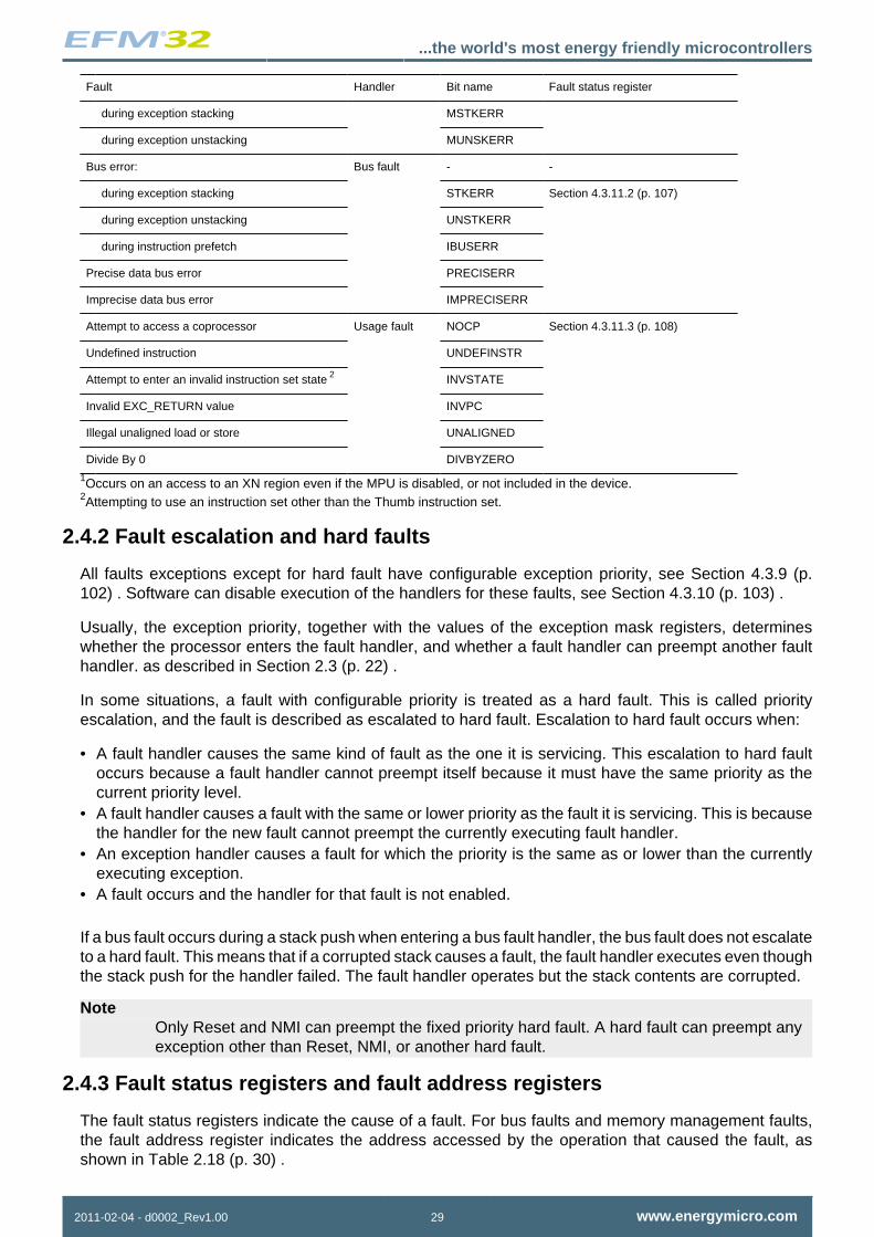
Table 2.17 (p. 28) shows the types of fault, the handler used for the fault, the corresponding faultstatus register, and the register bit that indicates that the fault has occurred. See Section 4.3.11 (p.105) for more information about the fault status registers.
Table 2.17. Faults
Fault Handler Bit name Fault status register
Bus error on a vector read VECTTBL
Fault escalated to a hard fault
Hard fault
FORCED
Section 4.3.12 (p. 109)
MPU mismatch: - -
on instruction access IACCVIOL 1
on data access
Memorymanagementfault
DACCVIOL
Section 4.3.11.1 (p. 105)
...the world's most energy friendly microcontrollers
2011-02-04 - d0002_Rev1.00 29 www.energymicro.com
Fault Handler Bit name Fault status register
during exception stacking MSTKERR
during exception unstacking MUNSKERR
Bus error: - -
during exception stacking STKERR
during exception unstacking UNSTKERR
during instruction prefetch IBUSERR
Precise data bus error PRECISERR
Imprecise data bus error
Bus fault
IMPRECISERR
Section 4.3.11.2 (p. 107)
Attempt to access a coprocessor NOCP
Undefined instruction UNDEFINSTR
Attempt to enter an invalid instruction set state 2 INVSTATE
Invalid EXC_RETURN value INVPC
Illegal unaligned load or store UNALIGNED
Divide By 0
Usage fault
DIVBYZERO
Section 4.3.11.3 (p. 108)
1Occurs on an access to an XN region even if the MPU is disabled, or not included in the device.2Attempting to use an instruction set other than the Thumb instruction set.
2.4.2 Fault escalation and hard faults
All faults exceptions except for hard fault have configurable exception priority, see Section 4.3.9 (p.102) . Software can disable execution of the handlers for these faults, see Section 4.3.10 (p. 103) .
Usually, the exception priority, together with the values of the exception mask registers, determineswhether the processor enters the fault handler, and whether a fault handler can preempt another faulthandler. as described in Section 2.3 (p. 22) .
In some situations, a fault with configurable priority is treated as a hard fault. This is called priorityescalation, and the fault is described as escalated to hard fault. Escalation to hard fault occurs when:
• A fault handler causes the same kind of fault as the one it is servicing. This escalation to hard faultoccurs because a fault handler cannot preempt itself because it must have the same priority as thecurrent priority level.
• A fault handler causes a fault with the same or lower priority as the fault it is servicing. This is becausethe handler for the new fault cannot preempt the currently executing fault handler.
• An exception handler causes a fault for which the priority is the same as or lower than the currentlyexecuting exception.
• A fault occurs and the handler for that fault is not enabled.
If a bus fault occurs during a stack push when entering a bus fault handler, the bus fault does not escalateto a hard fault. This means that if a corrupted stack causes a fault, the fault handler executes even thoughthe stack push for the handler failed. The fault handler operates but the stack contents are corrupted.
NoteOnly Reset and NMI can preempt the fixed priority hard fault. A hard fault can preempt anyexception other than Reset, NMI, or another hard fault.
2.4.3 Fault status registers and fault address registers
The fault status registers indicate the cause of a fault. For bus faults and memory management faults,the fault address register indicates the address accessed by the operation that caused the fault, asshown in Table 2.18 (p. 30) .

...the world's most energy friendly microcontrollers
2011-02-04 - d0002_Rev1.00 30 www.energymicro.com
Table 2.18. Fault status and fault address registers
Handler Status registername
Address registername
Register description
Hard fault HFSR - Section 4.3.12 (p. 109)
Memory managementfault
MMFSR MMFAR Section 4.3.11.1 (p. 105)
Section 4.3.13 (p. 110)
Bus fault BFSR BFAR Section 4.3.11.2 (p. 107)
Section 4.3.14 (p. 110)
Usage fault UFSR - Section 4.3.11.3 (p. 108)
2.4.4 Lockup
The processor enters a lockup state if a hard fault occurs when executing the NMI or hard fault handlers.When the processor is in lockup state it does not execute any instructions. The processor remains inlockup state until either:
• it is reset• an NMI occurs.
NoteIf lockup state occurs from the NMI handler a subsequent NMI does not cause theprocessor to leave lockup state.
2.5 Power managementThe Cortex-M3 processor sleep modes reduce power consumption:
• Sleep mode (Energy Mode 1) stops the processor clock• Deep sleep mode (Energy Mode 2/3) stops the high frequency oscillators and HFPERCLK/
HFCORECLK as well as flash memory.
The SLEEPDEEP bit of the SCR selects which sleep mode is used, see Section 4.3.7 (p. 100) . Formore information about the behavior of the sleep modes see the EMU documentation in the referencemanual for the device.
This section describes the mechanisms for entering sleep mode, and the conditions for waking up fromsleep mode.
2.5.1 Entering sleep mode
This section describes the mechanisms software can use to put the processor into sleep mode.
The system can generate spurious wakeup events, for example a debug operation wakes up theprocessor. Therefore software must be able to put the processor back into sleep mode after such anevent. A program might have an idle loop to put the processor back to sleep mode.
2.5.1.1 Wait for interrupt
The wait for interrupt instruction, WFI, causes immediate entry to sleep mode. When the processorexecutes a WFI instruction it stops executing instructions and enters sleep mode. See Section 3.10.12 (p.86) for more information.
2.5.1.2 Wait for event
The wait for event instruction, WFE, causes entry to sleep mode conditional on the value of an one-bitevent register. When the processor executes a WFE instruction, it checks this register:

...the world's most energy friendly microcontrollers
2011-02-04 - d0002_Rev1.00 31 www.energymicro.com
• if the register is 0 the processor stops executing instructions and enters sleep mode• if the register is 1 the processor clears the register to 0 and continues executing instructions without
entering sleep mode.
See Section 3.10.11 (p. 86) for more information.
If the event register is 1, this indicate that the processor must not enter sleep mode on executionof a WFE instruction. Typically, this is because the processor has executed an SEV instruction, seeSection 3.10.9 (p. 85) . Software cannot access this register directly.
2.5.1.3 Sleep-on-exit
If the SLEEPONEXIT bit of the SCR is set to 1, when the processor completes the execution of anexception handler it returns to Thread mode and immediately enters sleep mode. Use this mechanismin applications that only require the processor to run when an exception occurs.
2.5.2 Wakeup from sleep mode
The conditions for the processor to wakeup depend on the mechanism that cause it to enter sleep mode.
2.5.2.1 Wakeup from WFI or sleep-on-exit
Normally, the processor wakes up only when it detects an exception with sufficient priority to causeexception entry.
Some embedded systems might have to execute system restore tasks after the processor wakes up, andbefore it executes an interrupt handler. To achieve this set the PRIMASK bit to 1 and the FAULTMASKbit to 0. If an interrupt arrives that is enabled and has a higher priority than current exception priority,the processor wakes up but does not execute the interrupt handler until the processor sets PRIMASKto zero. For more information about PRIMASK and FAULTMASK see Section 2.1.3.6 (p. 11) .
2.5.2.2 Wakeup from WFE
The processor wakes up if:
• it detects an exception with sufficient priority to cause exception entry• in a multiprocessor system, another processor in the system executes an SEV instruction.
In addition, if the SEVONPEND bit in the SCR is set to 1, any new pending interrupt triggers an event andwakes up the processor, even if the interrupt is disabled or has insufficient priority to cause exceptionentry. For more information about the SCR see Section 4.3.7 (p. 100) .
2.5.3 The Wakeup Interrupt Controller
The Wakeup Interrupt Controller (WIC) is a peripheral that can detect an interrupt and wake theprocessor from deep sleep mode. The WIC is enabled only when the DEEPSLEEP bit in the SCR isset to 1, see Section 4.3.7 (p. 100) .
The WIC is not programmable, and does not have any registers or user interface. It operates entirelyfrom hardware signals.
When the WIC is enabled and the processor enters deep sleep mode, the power management unitin the system can power down most of the Cortex-M3 processor. This has the side effect of stoppingthe SysTick timer. When the WIC receives an interrupt, it takes a number of clock cycles to wakeupthe processor and restore its state, before it can process the interrupt. This means interrupt latency isincreased in deep sleep mode.
Note

...the world's most energy friendly microcontrollers
2011-02-04 - d0002_Rev1.00 32 www.energymicro.com
If the processor detects a connection to a debugger it disables the WIC.
2.5.4 Power management programming hints
ANSI C cannot directly generate the WFI and WFE instructions. The CMSIS provides the followingintrinsic functions for these instructions:
void __WFE(void) // Wait for Event
void __WFI(void) // Wait for Interrupt
...the world's most energy friendly microcontrollers
2011-02-04 - d0002_Rev1.00 33 www.energymicro.com
3 The Cortex-M3 Instruction Set
3.1 Instruction set summary
The processor implements a version of the Thumb instruction set. Table 3.1 (p. 33) lists the supportedinstructions.
NoteIn Table 3.1 (p. 33) :
• angle brackets, <>, enclose alternative forms of the operand• braces, {}, enclose optional operands• the Operands column is not exhaustive• Op2 is a flexible second operand that can be either a register or a constant• most instructions can use an optional condition code suffix.
For more information on the instructions and operands, see the instruction descriptions.
Table 3.1. Cortex-M3 instructions
Mnemonic Operands Brief description Flags Page
ADC, ADCS {Rd,} Rn, Op2 Add with Carry N,Z,C,V Section 3.5.1 (p.57)
ADD, ADDS {Rd,} Rn, Op2 Add N,Z,C,V Section 3.5.1 (p.57)
ADD, ADDW {Rd,} Rn, #imm12 Add N,Z,C,V Section 3.5.1 (p.57)
ADR Rd, label Load PC-relative address - Section 3.4.1 (p.46)
AND, ANDS {Rd,} Rn, Op2 Logical AND N,Z,C Section 3.5.2 (p.59)
ASR, ASRS Rd, Rm, <Rs|#n> Arithmetic Shift Right N,Z,C Section 3.5.3 (p.60)
B label Branch - Section 3.9.1 (p.74)
BFC Rd, #lsb, #width Bit Field Clear - Section 3.8.1 (p.71)
BFI Rd, Rn, #lsb,#width
Bit Field Insert - Section 3.8.1 (p.71)
BIC, BICS {Rd,} Rn, Op2 Bit Clear N,Z,C Section 3.5.2 (p.59)
BKPT #imm Breakpoint - Section 3.10.1 (p.80)
BL label Branch with Link - Section 3.9.1 (p.74)
BLX Rm Branch indirect with Link - Section 3.9.1 (p.74)
BX Rm Branch indirect - Section 3.9.1 (p.74)
CBNZ Rn, label Compare and Branch if Non Zero - Section 3.9.2 (p.75)
CBZ Rn, label Compare and Branch if Zero - Section 3.9.2 (p.75)

...the world's most energy friendly microcontrollers
2011-02-04 - d0002_Rev1.00 34 www.energymicro.com
Mnemonic Operands Brief description Flags Page
CLREX - Clear Exclusive - Section 3.4.9 (p.56)
CLZ Rd, Rm Count leading zeros - Section 3.5.4 (p.61)
CMN, CMNS Rn, Op2 Compare Negative N,Z,C,V Section 3.5.5 (p.62)
CMP, CMPS Rn, Op2 Compare N,Z,C,V Section 3.5.5 (p.62)
CPSID iflags Change Processor State, Disable Interrupts - Section 3.10.2 (p.80)
CPSIE iflags Change Processor State, Enable Interrupts - Section 3.10.2 (p.80)
DMB - Data Memory Barrier - Section 3.10.3 (p.81)
DSB - Data Synchronization Barrier - Section 3.10.4 (p.82)
EOR, EORS {Rd,} Rn, Op2 Exclusive OR N,Z,C Section 3.5.2 (p.59)
ISB - Instruction Synchronization Barrier - Section 3.10.5 (p.82)
IT - If#Then condition block - Section 3.9.3 (p.76)
LDM Rn{!}, reglist Load Multiple registers, increment after - Section 3.4.6 (p.52)
LDMDB,LDMEA
Rn{!}, reglist Load Multiple registers, decrement before - Section 3.4.6 (p.52)
LDMFD,LDMIA
Rn{!}, reglist Load Multiple registers, increment after - Section 3.4.6 (p.52)
LDR Rt, [Rn, #offset] Load Register with word - Section 3.4 (p.45)
LDRB, LDRBT Rt, [Rn, #offset] Load Register with byte - Section 3.4 (p.45)
LDRD Rt, Rt2, [Rn,#offset]
Load Register with two bytes - Section 3.4.2 (p.46)
LDREX Rt, [Rn, #offset] Load Register Exclusive - Section 3.4.8 (p.54)
LDREXB Rt, [Rn] Load Register Exclusive with byte - Section 3.4.8 (p.54)
LDREXH Rt, [Rn] Load Register Exclusive with halfword - Section 3.4.8 (p.54)
LDRH, LDRHT Rt, [Rn, #offset] Load Register with halfword - Section 3.4 (p.45)
LDRSB,LDRSBT
Rt, [Rn, #offset] Load Register with signed byte - Section 3.4 (p.45)
LDRSH,LDRSHT
Rt, [Rn, #offset] Load Register with signed halfword - Section 3.4 (p.45)
LDRT Rt, [Rn, #offset] Load Register with word - Section 3.4 (p.45)
LSL, LSLS Rd, Rm, <Rs|#n> Logical Shift Left N,Z,C Section 3.5.3 (p.60)
LSR, LSRS Rd, Rm, <Rs|#n> Logical Shift Right N,Z,C Section 3.5.3 (p.60)

...the world's most energy friendly microcontrollers
2011-02-04 - d0002_Rev1.00 35 www.energymicro.com
Mnemonic Operands Brief description Flags Page
MLA Rd, Rn, Rm, Ra Multiply with Accumulate, 32-bit result - Section 3.6.1 (p.67)
MLS Rd, Rn, Rm, Ra Multiply and Subtract, 32-bit result - Section 3.6.1 (p.67)
MOV, MOVS Rd, Op2 Move N,Z,C Section 3.5.6 (p.62)
MOVT Rd, #imm16 Move Top - Section 3.5.7 (p.64)
MOVW, MOV Rd, #imm16 Move 16-bit constant N,Z,C Section 3.5.6 (p.62)
MRS Rd, spec_reg Move from special register to general register - Section 3.10.6 (p.83)
MSR spec_reg, Rm Move from general register to special register N,Z,C,V Section 3.10.7 (p.83)
MUL, MULS {Rd,} Rn, Rm Multiply, 32-bit result N,Z Section 3.6.1 (p.67)
MVN, MVNS Rd, Op2 Move NOT N,Z,C Section 3.5.6 (p.62)
NOP - No Operation - Section 3.10.8 (p.84)
ORN, ORNS {Rd,} Rn, Op2 Logical OR NOT N,Z,C Section 3.5.2 (p.59)
ORR, ORRS {Rd,} Rn, Op2 Logical OR N,Z,C Section 3.5.2 (p.59)
POP reglist Pop registers from stack - Section 3.4.7 (p.53)
PUSH reglist Push registers onto stack - Section 3.4.7 (p.53)
RBIT Rd, Rn Reverse Bits - Section 3.5.8 (p.64)
REV Rd, Rn Reverse byte order in a word - Section 3.5.8 (p.64)
REV16 Rd, Rn Reverse byte order in each halfword - Section 3.5.8 (p.64)
REVSH Rd, Rn Reverse byte order in bottom halfword and signextend
- Section 3.5.8 (p.64)
ROR, RORS Rd, Rm, <Rs|#n> Rotate Right N,Z,C Section 3.5.3 (p.60)
RRX, RRXS Rd, Rm Rotate Right with Extend N,Z,C Section 3.5.3 (p.60)
RSB, RSBS {Rd,} Rn, Op2 Reverse Subtract N,Z,C,V Section 3.5.1 (p.57)
SBC, SBCS {Rd,} Rn, Op2 Subtract with Carry N,Z,C,V Section 3.5.1 (p.57)
SBFX Rd, Rn, #lsb,#width
Signed Bit Field Extract - Section 3.8.2 (p.72)
SDIV {Rd,} Rn, Rm Signed Divide - Section 3.6.3 (p.69)
SEV - Send Event - Section 3.10.9 (p.85)
SMLAL RdLo, RdHi, Rn, Rm Signed Multiply with Accumulate (32 x 32 + 64),64-bit result
- Section 3.6.2 (p.68)

...the world's most energy friendly microcontrollers
2011-02-04 - d0002_Rev1.00 36 www.energymicro.com
Mnemonic Operands Brief description Flags Page
SMULL RdLo, RdHi, Rn, Rm Signed Multiply (32 x 32), 64-bit result - Section 3.6.2 (p.68)
SSAT Rd, #n, Rm {,shift#s}
Signed Saturate Q Section 3.7.1 (p.69)
STM Rn{!}, reglist Store Multiple registers, increment after - Section 3.4.6 (p.52)
STMDB,STMEA
Rn{!}, reglist Store Multiple registers, decrement before - Section 3.4.6 (p.52)
STMFD,STMIA
Rn{!}, reglist Store Multiple registers, increment after - Section 3.4.6 (p.52)
STR Rt, [Rn, #offset] Store Register word - Section 3.4 (p.45)
STRB, STRBT Rt, [Rn, #offset] Store Register byte - Section 3.4 (p.45)
STRD Rt, Rt2, [Rn,#offset]
Store Register two words - Section 3.4.2 (p.46)
STREX Rd, Rt, [Rn,#offset]
Store Register Exclusive - Section 3.4.8 (p.54)
STREXB Rd, Rt, [Rn] Store Register Exclusive byte - Section 3.4.8 (p.54)
STREXH Rd, Rt, [Rn] Store Register Exclusive halfword - Section 3.4.8 (p.54)
STRH, STRHT Rt, [Rn, #offset] Store Register halfword - Section 3.4 (p.45)
STRT Rt, [Rn, #offset] Store Register word - Section 3.4 (p.45)
SUB, SUBS {Rd,} Rn, Op2 Subtract N,Z,C,V Section 3.5.1 (p.57)
SUB, SUBW {Rd,} Rn, #imm12 Subtract N,Z,C,V Section 3.5.1 (p.57)
SVC #imm Supervisor Call - Section 3.10.10 (p.85)
SXTB {Rd,} Rm {,ROR #n} Sign extend a byte - Section 3.8.3 (p.72)
SXTH {Rd,} Rm {,ROR #n} Sign extend a halfword - Section 3.8.3 (p.72)
TBB [Rn, Rm] Table Branch Byte - Section 3.9.4 (p.78)
TBH [Rn, Rm, LSL #1] Table Branch Halfword - Section 3.9.4 (p.78)
TEQ Rn, Op2 Test Equivalence N,Z,C Section 3.5.9 (p.65)
TST Rn, Op2 Test N,Z,C Section 3.5.9 (p.65)
UBFX Rd, Rn, #lsb,#width
Unsigned Bit Field Extract - Section 3.8.2 (p.72)
UDIV {Rd,} Rn, Rm Unsigned Divide - Section 3.6.3 (p.69)
UMLAL RdLo, RdHi, Rn, Rm Unsigned Multiply with Accumulate (32 x 32 + 64),64-bit result
- Section 3.6.2 (p.68)
UMULL RdLo, RdHi, Rn, Rm Unsigned Multiply (32 x 32), 64-bit result - Section 3.6.2 (p.68)
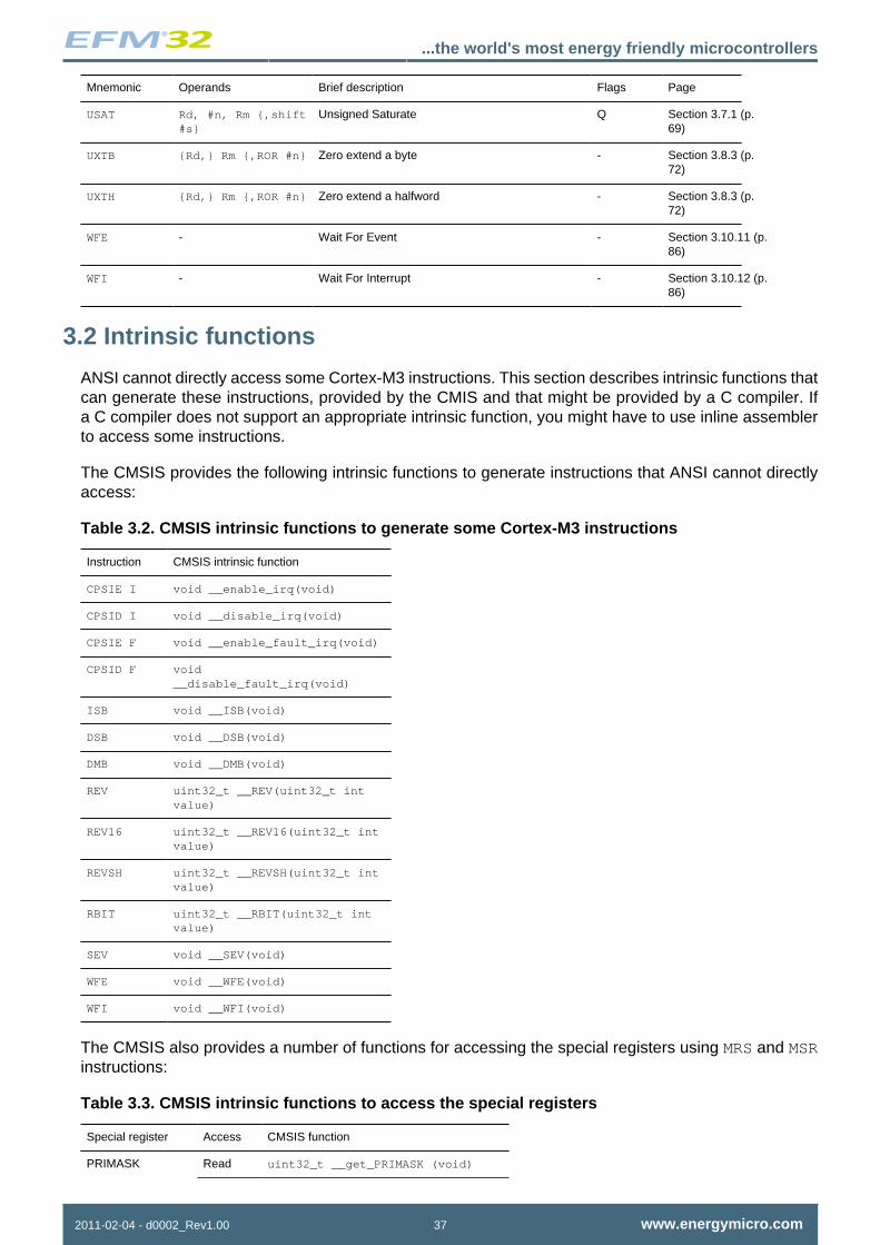
...the world's most energy friendly microcontrollers
2011-02-04 - d0002_Rev1.00 37 www.energymicro.com
Mnemonic Operands Brief description Flags Page
USAT Rd, #n, Rm {,shift#s}
Unsigned Saturate Q Section 3.7.1 (p.69)
UXTB {Rd,} Rm {,ROR #n} Zero extend a byte - Section 3.8.3 (p.72)
UXTH {Rd,} Rm {,ROR #n} Zero extend a halfword - Section 3.8.3 (p.72)
WFE - Wait For Event - Section 3.10.11 (p.86)
WFI - Wait For Interrupt - Section 3.10.12 (p.86)
3.2 Intrinsic functions
ANSI cannot directly access some Cortex-M3 instructions. This section describes intrinsic functions thatcan generate these instructions, provided by the CMIS and that might be provided by a C compiler. Ifa C compiler does not support an appropriate intrinsic function, you might have to use inline assemblerto access some instructions.
The CMSIS provides the following intrinsic functions to generate instructions that ANSI cannot directlyaccess:
Table 3.2. CMSIS intrinsic functions to generate some Cortex-M3 instructions
Instruction CMSIS intrinsic function
CPSIE I void __enable_irq(void)
CPSID I void __disable_irq(void)
CPSIE F void __enable_fault_irq(void)
CPSID F void__disable_fault_irq(void)
ISB void __ISB(void)
DSB void __DSB(void)
DMB void __DMB(void)
REV uint32_t __REV(uint32_t intvalue)
REV16 uint32_t __REV16(uint32_t intvalue)
REVSH uint32_t __REVSH(uint32_t intvalue)
RBIT uint32_t __RBIT(uint32_t intvalue)
SEV void __SEV(void)
WFE void __WFE(void)
WFI void __WFI(void)
The CMSIS also provides a number of functions for accessing the special registers using MRS and MSRinstructions:
Table 3.3. CMSIS intrinsic functions to access the special registers
Special register Access CMSIS function
PRIMASK Read uint32_t __get_PRIMASK (void)

...the world's most energy friendly microcontrollers
2011-02-04 - d0002_Rev1.00 38 www.energymicro.com
Special register Access CMSIS function
Write void __set_PRIMASK (uint32_tvalue)
Read uint32_t __get_FAULTMASK (void)FAULTMASK
Write void __set_FAULTMASK (uint32_tvalue)
Read uint32_t __get_BASEPRI (void)BASEPRI
Write void __set_BASEPRI (uint32_tvalue)
Read uint32_t __get_CONTROL (void)CONTROL
Write void __set_CONTROL (uint32_tvalue)
Read uint32_t __get_MSP (void)MSP
Write void __set_MSP (uint32_tTopOfMainStack)
Read uint32_t __get_PSP (void)PSP
Write void __set_PSP (uint32_tTopOfProcStack)
3.3 About the instruction descriptions
This section gives more information about using the instructions.
3.3.1 Operands
An instruction operand can be an ARM register, a constant, or another instruction-specific parameter.Instructions act on the operands and often store the result in a destination register. When there is adestination register in the instruction, it is usually specified before the operands.
Operands in some instructions are flexible in that they can either be a register or a constant. SeeSection 3.3.3 (p. 38) .
3.3.2 Restrictions when using PC or SP
Many instructions have restrictions on whether you can use the Program Counter (PC) or Stack Pointer(SP) for the operands or destination register. See instruction descriptions for more information.
NoteBit[0] of any address you write to the PC with a BX, BLX, LDM, LDR, or POP instruction mustbe 1 for correct execution, because this bit indicates the required instruction set, and theCortex-M3 processor only supports Thumb instructions.
3.3.3 Flexible second operand
Many general data processing instructions have a flexible second operand. This is shown as Operand2in the descriptions of the syntax of each instruction.
Operand2 can be a:
• Section 3.3.3.1 (p. 38)• Section 3.3.3.2 (p. 39)
3.3.3.1 Constant
You specify an Operand2 constant in the form:

...the world's most energy friendly microcontrollers
2011-02-04 - d0002_Rev1.00 39 www.energymicro.com
#constant
where constant can be:
• any constant that can be produced by shifting an 8#bit value left by any number of bits within a 32#bitword
• any constant of the form 0x00XY00XY• any constant of the form 0xXY00XY00• any constant of the form 0xXYXYXYXY.
NoteIn the constants shown above, X and Y are hexadecimal digits.
In addition, in a small number of instructions, constant can take a wider range of values. These aredescribed in the individual instruction descriptions.
When an Operand2 constant is used with the instructions MOVS, MVNS, ANDS, ORRS, ORNS, EORS, BICS,TEQ or TST, the carry flag is updated to bit[31] of the constant, if the constant is greater than 255 andcan be produced by shifting an 8-bit value. These instructions do not affect the carry flag if Operand2is any other constant.
3.3.3.1.1 Instruction substitution
Your assembler might be able to produce an equivalent instruction in cases where you specify a constantthat is not permitted. For example, an assembler might assemble the instruction CMP Rd, #0xFFFFFFFEas the equivalent instruction CMN Rd, #0x2.
3.3.3.2 Register with optional shift
You specify an Operand2 register in the form:
Rm {, shift}
where:
Rm is the register holding the data for the second operand.shift is an optional shift to be applied to Rm. It can be one of:
ASR #n arithmetic shift right n bits, 1 # n # 32.LSL #n logical shift left n bits, 1 # n # 31.LSR #n logical shift right n bits, 1 # n # 32.ROR #n rotate right n bits, 1 # n # 31.RRX rotate right one bit, with extend.- if omitted, no shift occurs, equivalent to LSL #0.
If you omit the shift, or specify LSL #0, the instruction uses the value in Rm.
If you specify a shift, the shift is applied to the value in Rm, and the resulting 32-bit value is used by theinstruction. However, the contents in the register Rm remains unchanged. Specifying a register with shiftalso updates the carry flag when used with certain instructions. For information on the shift operationsand how they affect the carry flag, see Section 3.3.4 (p. 39)
3.3.4 Shift Operations
Register shift operations move the bits in a register left or right by a specified number of bits, the shiftlength. Register shift can be performed:

...the world's most energy friendly microcontrollers
2011-02-04 - d0002_Rev1.00 40 www.energymicro.com
• directly by the instructions ASR, LSR, LSL, ROR, and RRX, and the result is written to a destinationregister
• during the calculation of Operand2 by the instructions that specify the second operand as a registerwith shift, see Section 3.3.3 (p. 38) . The result is used by the instruction.
The permitted shift lengths depend on the shift type and the instruction, see the individual instructiondescription or Section 3.3.3 (p. 38) . If the shift length is 0, no shift occurs. Register shift operationsupdate the carry flag except when the specified shift length is 0. The following sub-sections describethe various shift operations and how they affect the carry flag. In these descriptions, Rm is the registercontaining the value to be shifted, and n is the shift length.
3.3.4.1 ASR
Arithmetic shift right by n bits moves the left-hand 32-n bits of the register Rm, to the right by n places,into the right-hand 32-n bits of the result. And it copies the original bit[31] of the register into the left#handn bits of the result. See Figure 3.1 (p. 40) .
You can use the ASR #n operation to divide the value in the register Rm by 2n, with the result beingrounded towards negative-infinity.
When the instruction is ASRS or when ASR #n is used in Operand2 with the instructions MOVS, MVNS,ANDS, ORRS, ORNS, EORS, BICS, TEQ or TST, the carry flag is updated to the last bit shifted out, bit[n-1],of the register Rm.
Note• If n is 32 or more, then all the bits in the result are set to the value of bit[31] of Rm.• If n is 32 or more and the carry flag is updated, it is updated to the value of bit[31] of Rm.
Figure 3.1. ASR #3
31 1 0
CarryFlag
...
2345
3.3.4.2 LSR
Logical shift right by n bits moves the left-hand 32-n bits of the register Rm, to the right by n places, intothe right-hand 32-n bits of the result. And it sets the left#hand n bits of the result to 0. See Figure 3.2 (p.41) .
You can use the LSR #n operation to divide the value in the register Rm by 2n, if the value is regardedas an unsigned integer.
When the instruction is LSRS or when LSR #n is used in Operand2 with the instructions MOVS, MVNS,ANDS, ORRS, ORNS, EORS, BICS, TEQ or TST, the carry flag is updated to the last bit shifted out, bit[n-1],of the register Rm.
Note• If n is 32 or more, then all the bits in the result are cleared to 0.• If n is 33 or more and the carry flag is updated, it is updated to 0.

...the world's most energy friendly microcontrollers
2011-02-04 - d0002_Rev1.00 41 www.energymicro.com
Figure 3.2. LSR #3
31 1 0
CarryFlag
...
000
2345
3.3.4.3 LSL
Logical shift left by n bits moves the right-hand 32-n bits of the register Rm, to the left by n places, intothe left-hand 32-n bits of the result. And it sets the right#hand n bits of the result to 0. See Figure 3.3 (p.41) .
You can use he LSL #n operation to multiply the value in the register Rm by 2n, if the value is regardedas an unsigned integer or a two’s complement signed integer. Overflow can occur without warning.
When the instruction is LSLS or when LSL #n, with non-zero n, is used in Operand2 with the instructionsMOVS, MVNS, ANDS, ORRS, ORNS, EORS, BICS, TEQ or TST, the carry flag is updated to the last bit shiftedout, bit[32-n], of the register Rm. These instructions do not affect the carry flag when used with LSL #0.
Note• If n is 32 or more, then all the bits in the result are cleared to 0.• If n is 33 or more and the carry flag is updated, it is updated to 0.
Figure 3.3. LSL #3
31 1 0
CarryFlag ...
000
2345
3.3.4.4 ROR
Rotate right by n bits moves the left-hand 32-n bits of the register Rm, to the right by n places, into theright-hand 32-n bits of the result. And it moves the right#hand n bits of the register into the left#handn bits of the result. See Figure 3.4 (p. 42) .
When the instruction is RORS or when ROR #n is used in Operand2 with the instructions MOVS, MVNS,ANDS, ORRS, ORNS, EORS, BICS, TEQ or TST, the carry flag is updated to the last bit rotation, bit[n-1],of the register Rm.
Note• If n is 32, then the value of the result is same as the value in Rm, and if the carry flag is
updated, it is updated to bit[31] of Rm.• ROR with shift length, n, more than 32 is the same as ROR with shift length n-32.

...the world's most energy friendly microcontrollers
2011-02-04 - d0002_Rev1.00 42 www.energymicro.com
Figure 3.4. ROR #3
31 1 0
CarryFlag
...
2345
3.3.4.5 RRX
Rotate right with extend moves the bits of the register Rm to the right by one bit. And it copies the carryflag into bit[31] of the result. See Figure 3.5 (p. 42) .
When the instruction is RRXS or when RRX is used in Operand2 with the instructions MOVS, MVNS, ANDS,ORRS, ORNS, EORS, BICS, TEQ or TST, the carry flag is updated to bit[0] of the register Rm.
Figure 3.5. RRX
31 30 1 0
CarryFlag
... ...
3.3.5 Address alignment
An aligned access is an operation where a word-aligned address is used for a word, dual word, ormultiple word access, or where a halfword-aligned address is used for a halfword access. Byte accessesare always aligned.
The Cortex-M3 processor supports unaligned access only for the following instructions:
• LDR, LDRT• LDRH, LDRHT• LDRSH, LDRSHT• STR, STRT• STRH, STRHT
All other load and store instructions generate a usage fault exception if they perform an unaligned access,and therefore their accesses must be address aligned. For more information about usage faults seeSection 2.4 (p. 28) .
Unaligned accesses are usually slower than aligned accesses. In addition, some memory regions mightnot support unaligned accesses. Therefore, ARM recommends that programmers ensure that accessesare aligned. To avoid accidental generation of unaligned accesses, use the UNALIGN_TRP bit in theConfiguration and Control Register to trap all unaligned accesses, see Section 4.3.8 (p. 101) .
3.3.6 PC#relative expressions
A PC#relative expression or label is a symbol that represents the address of an instruction or literaldata. It is represented in the instruction as the PC value plus or minus a numeric offset. The assemblercalculates the required offset from the label and the address of the current instruction. If the offset is toobig, the assembler produces an error.

...the world's most energy friendly microcontrollers
2011-02-04 - d0002_Rev1.00 43 www.energymicro.com
Note• For B, BL, CBNZ, and CBZ instructions, the value of the PC is the address of the current
instruction plus 4 bytes.• For all other instructions that use labels, the value of the PC is the address of the current
instruction plus 4 bytes, with bit[1] of the result cleared to 0 to make it word-aligned.• Your assembler might permit other syntaxes for PC-relative expressions, such as a label
plus or minus a number, or an expression of the form [PC, #number].
3.3.7 Conditional execution
Most data processing instructions can optionally update the condition flags in the Application ProgramStatus Register (APSR) according to the result of the operation, see Section 2.1.3.5.1 (p. 9) . Someinstructions update all flags, and some only update a subset. If a flag is not updated, the original valueis preserved. See the instruction descriptions for the flags they affect.
You can execute an instruction conditionally, based on the condition flags set in another instruction,either:
• immediately after the instruction that updated the flags• after any number of intervening instructions that have not updated the flags.
Conditional execution is available by using conditional branches or by adding condition code suffixesto instructions. See Table 3.4 (p. 44) for a list of the suffixes to add to instructions to make themconditional instructions. The condition code suffix enables the processor to test a condition based onthe flags. If the condition test of a conditional instruction fails, the instruction:
• does not execute• does not write any value to its destination register• does not affect any of the flags• does not generate any exception.
Conditional instructions, except for conditional branches, must be inside an If-Then instruction block. SeeSection 3.9.3 (p. 76) for more information and restrictions when using the IT instruction. Dependingon the vendor, the assembler might automatically insert an IT instruction if you have conditionalinstructions outside the IT block.
Use the CBZ and CBNZ instructions to compare the value of a register against zero and branch on theresult.
This section describes:
• Section 3.3.7.1 (p. 43)• Section 3.3.7.2 (p. 44) .
3.3.7.1 The condition flags
The APSR contains the following condition flags:
N Set to 1 when the result of the operation was negative, cleared to 0 otherwise.Z Set to 1 when the result of the operation was zero, cleared to 0 otherwise.C Set to 1 when the operation resulted in a carry, cleared to 0 otherwise.V Set to 1 when the operation caused overflow, cleared to 0 otherwise.
For more information about the APSR see Section 2.1.3.5 (p. 8) .
A carry occurs:

...the world's most energy friendly microcontrollers
2011-02-04 - d0002_Rev1.00 44 www.energymicro.com
• if the result of an addition is greater than or equal to 232
• if the result of a subtraction is positive or zero• as the result of an inline barrel shifter operation in a move or logical instruction.
Overflow occurs if the result of an add, subtract, or compare is greater than or equal to 231, or lessthan –231.
NoteMost instructions update the status flags only if the S suffix is specified. See the instructiondescriptions for more information.
3.3.7.2 Condition code suffixes
The instructions that can be conditional have an optional condition code, shown in syntax descriptionsas {cond}. Conditional execution requires a preceding IT instruction. An instruction with a conditioncode is only executed if the condition code flags in the APSR meet the specified condition. Table 3.4 (p.44) shows the condition codes to use.
You can use conditional execution with the IT instruction to reduce the number of branch instructionsin code.
Table 3.4 (p. 44) also shows the relationship between condition code suffixes and the N, Z, C, andV flags.
Table 3.4. Condition code suffixes
Suffix Flags Meaning
EQ Z = 1 Equal
NE Z = 0 Not equal
CS orHS
C = 1 Higher or same, unsigned #
CC orLO
C = 0 Lower, unsigned <
MI N = 1 Negative
PL N = 0 Positive or zero
VS V = 1 Overflow
VC V = 0 No overflow
HI C = 1 and Z = 0 Higher, unsigned >
LS C = 0 or Z = 1 Lower or same, unsigned #
GE N = V Greater than or equal, signed #
LT N != V Less than, signed <
GT Z = 0 and N = V Greater than, signed >
LE Z = 1 and N != V Less than or equal, signed #
AL Can have any value Always. This is the default when no suffix is specified.
Example 3.1 (p. 44) shows the use of a conditional instruction to find the absolute value of a number.R0 = ABS(R1).
Example 3.1. Absolute value
MOVS R0, R1 ; R0 = R1, setting flags IT MI ; IT instruction for the negative condition RSBMI R0, R1, #0 ; If negative, R0 = -R1
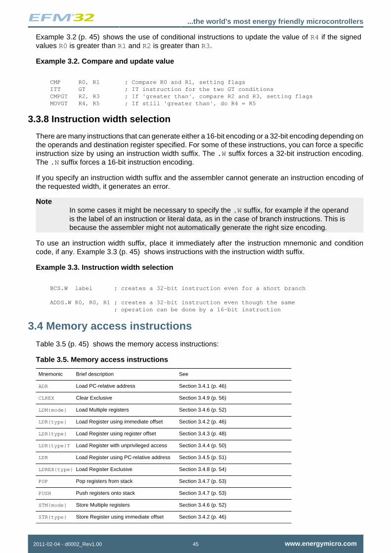
...the world's most energy friendly microcontrollers
2011-02-04 - d0002_Rev1.00 45 www.energymicro.com
Example 3.2 (p. 45) shows the use of conditional instructions to update the value of R4 if the signedvalues R0 is greater than R1 and R2 is greater than R3.
Example 3.2. Compare and update value
CMP R0, R1 ; Compare R0 and R1, setting flags ITT GT ; IT instruction for the two GT conditions CMPGT R2, R3 ; If 'greater than', compare R2 and R3, setting flags MOVGT R4, R5 ; If still 'greater than', do R4 = R5
3.3.8 Instruction width selection
There are many instructions that can generate either a 16-bit encoding or a 32-bit encoding depending onthe operands and destination register specified. For some of these instructions, you can force a specificinstruction size by using an instruction width suffix. The .W suffix forces a 32-bit instruction encoding.The .N suffix forces a 16-bit instruction encoding.
If you specify an instruction width suffix and the assembler cannot generate an instruction encoding ofthe requested width, it generates an error.
NoteIn some cases it might be necessary to specify the .W suffix, for example if the operandis the label of an instruction or literal data, as in the case of branch instructions. This isbecause the assembler might not automatically generate the right size encoding.
To use an instruction width suffix, place it immediately after the instruction mnemonic and conditioncode, if any. Example 3.3 (p. 45) shows instructions with the instruction width suffix.
Example 3.3. Instruction width selection
BCS.W label ; creates a 32-bit instruction even for a short branch
ADDS.W R0, R0, R1 ; creates a 32-bit instruction even though the same ; operation can be done by a 16-bit instruction
3.4 Memory access instructions
Table 3.5 (p. 45) shows the memory access instructions:
Table 3.5. Memory access instructions
Mnemonic Brief description See
ADR Load PC-relative address Section 3.4.1 (p. 46)
CLREX Clear Exclusive Section 3.4.9 (p. 56)
LDM{mode} Load Multiple registers Section 3.4.6 (p. 52)
LDR{type} Load Register using immediate offset Section 3.4.2 (p. 46)
LDR{type} Load Register using register offset Section 3.4.3 (p. 48)
LDR{type}T Load Register with unprivileged access Section 3.4.4 (p. 50)
LDR Load Register using PC-relative address Section 3.4.5 (p. 51)
LDREX{type} Load Register Exclusive Section 3.4.8 (p. 54)
POP Pop registers from stack Section 3.4.7 (p. 53)
PUSH Push registers onto stack Section 3.4.7 (p. 53)
STM{mode} Store Multiple registers Section 3.4.6 (p. 52)
STR{type} Store Register using immediate offset Section 3.4.2 (p. 46)

...the world's most energy friendly microcontrollers
2011-02-04 - d0002_Rev1.00 46 www.energymicro.com
Mnemonic Brief description See
STR{type} Store Register using register offset Section 3.4.3 (p. 48)
STR{type}T Store Register with unprivileged access Section 3.4.4 (p. 50)
STREX{type} Store Register Exclusive Section 3.4.8 (p. 54)
3.4.1 ADR
Load PC-relative address.
3.4.1.1 Syntax
ADR{cond} Rd, label
where:
cond is an optional condition code, see Section 3.3.7 (p. 43) .Rd is the destination register.label is a PC#relative expression. See Section 3.3.6 (p. 42) .
3.4.1.2 Operation
ADR determines the address by adding an immediate value to the PC, and writes the result to thedestination register.
ADR produces position#independent code, because the address is PC#relative.
If you use ADR to generate a target address for a BX or BLX instruction, you must ensure that bit[0] ofthe address you generate is set to1 for correct execution.
Values of label must be within the range of #4095 to +4095 from the address in the PC.
NoteYou might have to use the .W suffix to get the maximum offset range or to generateaddresses that are not word-aligned. See Section 3.3.8 (p. 45) .
3.4.1.3 Restrictions
Rd must not be SP and must not be PC.
3.4.1.4 Condition flags
This instruction does not change the flags.
3.4.1.5 Examples
ADR R1, TextMessage ; Write address value of a location labelled as ; TextMessage to R1
3.4.2 LDR and STR, immediate offset
Load and Store with immediate offset, pre-indexed immediate offset, or post-indexed immediate offset.
3.4.2.1 Syntax
op{type}{cond} Rt, [Rn {, #offset}] ; immediate offset

...the world's most energy friendly microcontrollers
2011-02-04 - d0002_Rev1.00 47 www.energymicro.com
op{type}{cond} Rt, [Rn, #offset]! ; pre-indexed
op{type}{cond} Rt, [Rn], #offset ; post-indexed
opD{cond} Rt, Rt2, [Rn {, #offset}] ; immediate offset, two words
opD{cond} Rt, Rt2, [Rn, #offset]! ; pre-indexed, two words
opD{cond} Rt, Rt2, [Rn], #offset ; post-indexed, two words
where:
op is one of:LDR Load Register.STR Store Register.
type is one of:B unsigned byte, zero extend to 32 bits on loads.SB signed byte, sign extend to 32 bits (LDR only).H unsigned halfword, zero extend to 32 bits on loads.SH signed halfword, sign extend to 32 bits (LDR only).# omit, for word.
cond is an optional condition code, see Section 3.3.7 (p. 43) .Rt is the register to load or store.Rn is the register on which the memory address is based.offset is an offset from Rn. If offset is omitted, the address is the contents of Rn.Rt2 is the additional register to load or store for two-word operations.
3.4.2.2 Operation
LDR instructions load one or two registers with a value from memory.
STR instructions store one or two register values to memory.
Load and store instructions with immediate offset can use the following addressing modes:
Offset addressing The offset value is added to or subtracted from the address obtainedfrom the register Rn. The result is used as the address for the memoryaccess. The register Rn is unaltered. The assembly language syntaxfor this mode is:
[Rn, #offset]
Pre-indexed addressing The offset value is added to or subtracted from the address obtainedfrom the register Rn. The result is used as the address for the memoryaccess and written back into the register Rn. The assembly languagesyntax for this mode is:
[Rn, #offset]!
Post-indexed addressing The address obtained from the register Rn is used as the addressfor the memory access. The offset value is added to or subtractedfrom the address, and written back into the register Rn. The assemblylanguage syntax for this mode is:
[Rn], #offset

...the world's most energy friendly microcontrollers
2011-02-04 - d0002_Rev1.00 48 www.energymicro.com
The value to load or store can be a byte, halfword, word, or two words. Bytes and halfwords can eitherbe signed or unsigned. See Section 3.3.5 (p. 42) .
Table 3.6 (p. 48) shows the ranges of offset for immediate, pre-indexed and post-indexed forms.
Table 3.6. Offset ranges
Instruction type Immediate offset Pre-indexed Post-indexed
Word, halfword, signedhalfword, byte, or signed byte
#255 to 4095 #255 to 255 #255 to 255
Two words multiple of 4 in therange #1020 to 1020
multiple of 4 in therange #1020 to 1020
multiple of 4 in therange #1020 to 1020
3.4.2.3 Restrictions
For load instructions:
• Rt can be SP or PC for word loads only• Rt must be different from Rt2 for two-word loads• Rn must be different from Rt and Rt2 in the pre-indexed or post-indexed forms.
When Rt is PC in a word load instruction:
• bit[0] of the loaded value must be 1 for correct execution• a branch occurs to the address created by changing bit[0] of the loaded value to 0• if the instruction is conditional, it must be the last instruction in the IT block.
For store instructions:
• Rt can be SP for word stores only• Rt must not be PC• Rn must not be PC• Rn must be different from Rt and Rt2 in the pre-indexed or post-indexed forms.
3.4.2.4 Condition flags
These instructions do not change the flags.
3.4.2.5 Examples
LDR R8, [R10] ; Loads R8 from the address in R10. LDRNE R2, [R5, #960]! ; Loads (conditionally) R2 from a word ; 960 bytes above the address in R5, and ; increments R5 by 960. STR R2, [R9,#const#struc] ; const#struc is an expression evaluating ; to a constant in the range 0#4095. STRH R3, [R4], #4 ; Store R3 as halfword data into address in ; R4, then increment R4 by 4 LDRD R8, R9, [R3, #0x20] ; Load R8 from a word 32 bytes above the ; address in R3, and load R9 from a word 36 ; bytes above the address in R3 STRD R0, R1, [R8], #-16 ; Store R0 to address in R8, and store R1 to ; a word 4 bytes above the address in R8, ; and then decrement R8 by 16.
3.4.3 LDR and STR, register offset
Load and Store with register offset.

...the world's most energy friendly microcontrollers
2011-02-04 - d0002_Rev1.00 49 www.energymicro.com
3.4.3.1 Syntax
op{type}{cond} Rt, [Rn, Rm {, LSL #n}]
where:
op is one of:LDR Load Register.STR Store Register.
type is one of:B unsigned byte, zero extend to 32 bits on loads.SB signed byte, sign extend to 32 bits (LDR only).H unsigned halfword, zero extend to 32 bits on loads.SH signed halfword, sign extend to 32 bits (LDR only).# omit, for word.
cond is an optional condition code, see Section 3.3.7 (p. 43) .Rt is the register to load or store.Rn is the register on which the memory address is based.Rm is a register containing a value to be used as the offset.LSL #n is an optional shift, with n in the range 0 to 3.
3.4.3.2 Operation
LDR instructions load a register with a value from memory.
STR instructions store a register value into memory.
The memory address to load from or store to is at an offset from the register Rn. The offset is specifiedby the register Rm and can be shifted left by up to 3 bits using LSL.
The value to load or store can be a byte, halfword, or word. For load instructions, bytes and halfwordscan either be signed or unsigned. See Section 3.3.5 (p. 42) .
3.4.3.3 Restrictions
In these instructions:
• Rn must not be PC• Rm must not be SP and must not be PC• Rt can be SP only for word loads and word stores• Rt can be PC only for word loads.
When Rt is PC in a word load instruction:
• bit[0] of the loaded value must be 1 for correct execution, and a branch occurs to this halfword-alignedaddress
• if the instruction is conditional, it must be the last instruction in the IT block.
3.4.3.4 Condition flags
These instructions do not change the flags.
3.4.3.5 Examples
STR R0, [R5, R1] ; Store value of R0 into an address equal to ; sum of R5 and R1
...the world's most energy friendly microcontrollers
2011-02-04 - d0002_Rev1.00 50 www.energymicro.com
LDRSB R0, [R5, R1, LSL #1] ; Read byte value from an address equal to ; sum of R5 and two times R1, sign extended it ; to a word value and put it in R0 STR R0, [R1, R2, LSL #2] ; Stores R0 to an address equal to sum of R1 ; and four times R2
3.4.4 LDR and STR, unprivileged
Load and Store with unprivileged access.
3.4.4.1 Syntax
op{type}T{cond} Rt, [Rn {, #offset}] ; immediate offset
where:
op is one of:LDR Load Register.STR Store Register.
type is one of:B unsigned byte, zero extend to 32 bits on loads.SB signed byte, sign extend to 32 bits (LDR only).H unsigned halfword, zero extend to 32 bits on loads.SH signed halfword, sign extend to 32 bits (LDR only).# omit, for word.
cond is an optional condition code, see Section 3.3.7 (p. 43) .Rt is the register to load or store.Rn is the register on which the memory address is based.offset is an offset from Rn and can be 0 to 255. If offset is omitted, the address is the value in Rn.
3.4.4.2 Operation
These load and store instructions perform the same function as the memory access instructions withimmediate offset, see Section 3.4.2 (p. 46) . The difference is that these instructions have onlyunprivileged access even when used in privileged software.
When used in unprivileged software, these instructions behave in exactly the same way as normalmemory access instructions with immediate offset.
3.4.4.3 Restrictions
In these instructions:
• Rn must not be PC• Rt must not be SP and must not be PC.
3.4.4.4 Condition flags
These instructions do not change the flags.
3.4.4.5 Examples
STRBTEQ R4, [R7] ; Conditionally store least significant byte in ; R4 to an address in R7, with unprivileged access LDRHT R2, [R2, #8] ; Load halfword value from an address equal to ; sum of R2 and 8 into R2, with unprivileged access

...the world's most energy friendly microcontrollers
2011-02-04 - d0002_Rev1.00 51 www.energymicro.com
3.4.5 LDR, PC#relative
Load register from memory.
3.4.5.1 Syntax
LDR{type}{cond} Rt, label
LDRD{cond} Rt, Rt2, label ; Load two words
where:
type is one of:B unsigned byte, zero extend to 32 bits.SB signed byte, sign extend to 32 bits.H unsigned halfword, zero extend to 32 bits.SH signed halfword, sign extend to 32 bits.# omit, for word.
cond is an optional condition code, see Section 3.3.7 (p. 43) .Rt is the register to load or store.Rt2 is the second register to load or store.label is a PC#relative expression. See Section 3.3.6 (p. 42) .
3.4.5.2 Operation
LDR loads a register with a value from a PC-relative memory address. The memory address is specifiedby a label or by an offset from the PC.
The value to load or store can be a byte, halfword, or word. For load instructions, bytes and halfwordscan either be signed or unsigned. See Section 3.3.5 (p. 42) .
label must be within a limited range of the current instruction. Table 3.7 (p. 51) shows the possibleoffsets between label and the PC.
Table 3.7. Offset ranges
Instruction type Offset range
Word, halfword, signed halfword, byte, signed byte #4095 to 4095
Two words #1020 to 1020
NoteYou might have to use the .W suffix to get the maximum offset range. See Section 3.3.8 (p.45) .
3.4.5.3 Restrictions
In these instructions:
• Rt can be SP or PC only for word loads• Rt2 must not be SP and must not be PC• Rt must be different from Rt2.
When Rt is PC in a word load instruction:
• bit[0] of the loaded value must be 1 for correct execution, and a branch occurs to this halfword-alignedaddress

...the world's most energy friendly microcontrollers
2011-02-04 - d0002_Rev1.00 52 www.energymicro.com
• if the instruction is conditional, it must be the last instruction in the IT block.
3.4.5.4 Condition flags
These instructions do not change the flags.
3.4.5.5 Examples
LDR R0, LookUpTable ; Load R0 with a word of data from an address ; labelled as LookUpTable LDRSB R7, localdata ; Load a byte value from an address labelled ; as localdata, sign extend it to a word ; value, and put it in R7
3.4.6 LDM and STM
Load and Store Multiple registers.
3.4.6.1 Syntax
op{addr_mode}{cond} Rn{!}, reglist
where:
op is one of:LDM Load Multiple registers.STM Store Multiple registers.
addr_mode is any one of the following:IA Increment address After each access. This is the default.DB Decrement address Before each access.
cond is an optional condition code, see Section 3.3.7 (p. 43) .Rn is the register on which the memory addresses are based.! is an optional writeback suffix. If ! is present the final address, that is loaded from or
stored to, is written back into Rn.reglist is a list of one or more registers to be loaded or stored, enclosed in braces. It can contain
register ranges. It must be comma separated if it contains more than one register orregister range, see Section 3.4.6.5 (p. 53) .
LDM and LDMFD are synonyms for LDMIA. LDMFD refers to its use for popping data from Full Descendingstacks.
LDMEA is a synonym for LDMDB, and refers to its use for popping data from Empty Ascending stacks.
STM and STMEA are synonyms for STMIA. STMEA refers to its use for pushing data onto Empty Ascendingstacks.
STMFD is s synonym for STMDB, and refers to its use for pushing data onto Full Descending stacks
3.4.6.2 Operation
LDM instructions load the registers in reglist with word values from memory addresses based on Rn.
STM instructions store the word values in the registers in reglist to memory addresses based on Rn.
For LDM, LDMIA, LDMFD, STM, STMIA, and STMEA the memory addresses used for the accesses areat 4-byte intervals ranging from Rn to Rn + 4 * (n-1), where n is the number of registers in reglist.The accesses happens in order of increasing register numbers, with the lowest numbered register using

...the world's most energy friendly microcontrollers
2011-02-04 - d0002_Rev1.00 53 www.energymicro.com
the lowest memory address and the highest number register using the highest memory address. If thewriteback suffix is specified, the value of Rn + 4 * (n-1) is written back to Rn.
For LDMDB, LDMEA, STMDB, and STMFD the memory addresses used for the accesses are at 4-byteintervals ranging from Rn to Rn - 4 * (n-1), where n is the number of registers in reglist. The accesseshappen in order of decreasing register numbers, with the highest numbered register using the highestmemory address and the lowest number register using the lowest memory address. If the writebacksuffix is specified, the value of Rn - 4 * (n-1) is written back to Rn.
The PUSH and POP instructions can be expressed in this form. See Section 3.4.7 (p. 53) for details.
3.4.6.3 Restrictions
In these instructions:
• Rn must not be PC• reglist must not contain SP• in any STM instruction, reglist must not contain PC• in any LDM instruction, reglist must not contain PC if it contains LR• reglist must not contain Rn if you specify the writeback suffix.
When PC is in reglist in an LDM instruction:
• bit[0] of the value loaded to the PC must be 1 for correct execution, and a branch occurs to thishalfword-aligned address
• if the instruction is conditional, it must be the last instruction in the IT block.
3.4.6.4 Condition flags
These instructions do not change the flags.
3.4.6.5 Examples
LDM R8,{R0,R2,R9} ; LDMIA is a synonym for LDM STMDB R1!,{R3#R6,R11,R12}
3.4.6.6 Incorrect examples
STM R5!,{R5,R4,R9} ; Value stored for R5 is unpredictable LDM R2, {} ; There must be at least one register in the list
3.4.7 PUSH and POP
Push registers onto, and pop registers off a full-descending stack.
3.4.7.1 Syntax
PUSH{cond} reglist
POP{cond} reglist
where:
cond is an optional condition code, see Section 3.3.7 (p. 43) .reglist is a non-empty list of registers, enclosed in braces. It can contain register ranges. It must be
comma separated if it contains more than one register or register range.

...the world's most energy friendly microcontrollers
2011-02-04 - d0002_Rev1.00 54 www.energymicro.com
PUSH and POP are synonyms for STMDB and LDM (or LDMIA) with the memory addresses for the accessbased on SP, and with the final address for the access written back to the SP. PUSH and POP are thepreferred mnemonics in these cases.
3.4.7.2 Operation
PUSH stores registers on the stack in order of decreasing the register numbers, with the highestnumbered register using the highest memory address and the lowest numbered register using the lowestmemory address.
POP loads registers from the stack in order of increasing register numbers, with the lowest numberedregister using the lowest memory address and the highest numbered register using the highest memoryaddress.
See Section 3.4.6 (p. 52) for more information.
3.4.7.3 Restrictions
In these instructions:
• reglist must not contain SP• for the PUSH instruction, reglist must not contain PC• for the POP instruction, reglist must not contain PC if it contains LR.
When PC is in reglist in a POP instruction:
• bit[0] of the value loaded to the PC must be 1 for correct execution, and a branch occurs to thishalfword-aligned address
• if the instruction is conditional, it must be the last instruction in the IT block.
3.4.7.4 Condition flags
These instructions do not change the flags.
3.4.7.5 Examples
PUSH {R0,R4#R7} PUSH {R2,LR} POP {R0,R10,PC}
3.4.8 LDREX and STREX
Load and Store Register Exclusive.
3.4.8.1 Syntax
LDREX{cond} Rt, [Rn {, #offset}]
STREX{cond} Rd, Rt, [Rn {, #offset}]
LDREXB{cond} Rt, [Rn]
STREXB{cond} Rd, Rt, [Rn]
LDREXH{cond} Rt, [Rn]

...the world's most energy friendly microcontrollers
2011-02-04 - d0002_Rev1.00 55 www.energymicro.com
STREXH{cond} Rd, Rt, [Rn]
where:
cond is an optional condition code, see Section 3.3.7 (p. 43) .Rd is the destination register for the returned status.Rt is the register to load or store.Rn is the register on which the memory address is based.offset is an optional offset applied to the value in Rn. If offset is omitted, the address is the value
in Rn.
3.4.8.2 Operation
LDREX, LDREXB, and LDREXH load a word, byte, and halfword respectively from a memory address.
STREX, STREXB, and STREXH attempt to store a word, byte, and halfword respectively to a memoryaddress. The address used in any Store-Exclusive instruction must be the same as the address in themost recently executed Load-exclusive instruction. The value stored by the Store-Exclusive instructionmust also have the same data size as the value loaded by the preceding Load-exclusive instruction.This means software must always use a Load-exclusive instruction and a matching Store-Exclusiveinstruction to perform a synchronization operation, see Section 2.2.7 (p. 20)
If an Store-Exclusive instruction performs the store, it writes 0 to its destination register. If it does notperform the store, it writes 1 to its destination register. If the Store-Exclusive instruction writes 0 to thedestination register, it is guaranteed that no other process in the system has accessed the memorylocation between the Load-exclusive and Store-Exclusive instructions.
For reasons of performance, keep the number of instructions between corresponding Load-Exclusiveand Store-Exclusive instruction to a minimum.
NoteThe result of executing a Store-Exclusive instruction to an address that is different from thatused in the preceding Load-Exclusive instruction is unpredictable.
3.4.8.3 Restrictions
In these instructions:
• do not use PC• do not use SP for Rd and Rt• for STREX, Rd must be different from both Rt and Rn• the value of offset must be a multiple of four in the range 0-1020.
3.4.8.4 Condition flags
These instructions do not change the flags.
3.4.8.5 Examples
MOV R1, #0x1 ; Initialize the ‘lock taken’ valuetry LDREX R0, [LockAddr] ; Load the lock value CMP R0, #0 ; Is the lock free? ITT EQ ; IT instruction for STREXEQ and CMPEQ STREXEQ R0, R1, [LockAddr] ; Try and claim the lock CMPEQ R0, #0 ; Did this succeed? BNE try ; No – try again .... ; Yes – we have the lock

...the world's most energy friendly microcontrollers
2011-02-04 - d0002_Rev1.00 56 www.energymicro.com
3.4.9 CLREX
Clear Exclusive.
3.4.9.1 Syntax
CLREX{cond}
where:
cond is an optional condition code, see Section 3.3.7 (p. 43) .
3.4.9.2 Operation
Use CLREX to make the next STREX, STREXB, or STREXH instruction write 1 to its destination register andfail to perform the store. It is useful in exception handler code to force the failure of the store exclusive ifthe exception occurs between a load exclusive instruction and the matching store exclusive instructionin a synchronization operation.
See Section 2.2.7 (p. 20) for more information.
3.4.9.3 Condition flags
These instructions do not change the flags.
3.4.9.4 Examples
CLREX
3.5 General data processing instructions
Table 3.8 (p. 56) shows the data processing instructions:
Table 3.8. Data processing instructions
Mnemonic Brief description See
ADC Add with Carry Section 3.5.1 (p. 57)
ADD Add Section 3.5.1 (p. 57)
ADDW Add Section 3.5.1 (p. 57)
AND Logical AND Section 3.5.2 (p. 59)
ASR Arithmetic Shift Right Section 3.5.3 (p. 60)
BIC Bit Clear Section 3.5.2 (p. 59)
CLZ Count leading zeros Section 3.5.4 (p. 61)
CMN Compare Negative Section 3.5.5 (p. 62)
CMP Compare Section 3.5.5 (p. 62)
EOR Exclusive OR Section 3.5.2 (p. 59)
LSL Logical Shift Left Section 3.5.3 (p. 60)
LSR Logical Shift Right Section 3.5.3 (p. 60)
MOV Move Section 3.5.6 (p. 62)
MOVT Move Top Section 3.5.7 (p. 64)
MOVW Move 16-bit constant Section 3.5.6 (p. 62)

...the world's most energy friendly microcontrollers
2011-02-04 - d0002_Rev1.00 57 www.energymicro.com
Mnemonic Brief description See
MVN Move NOT Section 3.5.6 (p. 62)
ORN Logical OR NOT Section 3.5.2 (p. 59)
ORR Logical OR Section 3.5.2 (p. 59)
RBIT Reverse Bits Section 3.5.8 (p. 64)
REV Reverse byte order in a word Section 3.5.8 (p. 64)
REV16 Reverse byte order in each halfword Section 3.5.8 (p. 64)
REVSH Reverse byte order in bottom halfword and sign extend Section 3.5.8 (p. 64)
ROR Rotate Right Section 3.5.3 (p. 60)
RRX Rotate Right with Extend Section 3.5.3 (p. 60)
RSB Reverse Subtract Section 3.5.1 (p. 57)
SBC Subtract with Carry Section 3.5.1 (p. 57)
SUB Subtract Section 3.5.1 (p. 57)
SUBW Subtract Section 3.5.1 (p. 57)
TEQ Test Equivalence Section 3.5.9 (p. 65)
TST Test Section 3.5.9 (p. 65)
3.5.1 ADD, ADC, SUB, SBC, and RSB
Add, Add with carry, Subtract, Subtract with carry, and Reverse Subtract.
3.5.1.1 Syntax
op{S}{cond} {Rd,} Rn, Operand2
op{cond} {Rd,} Rn, #imm12 ; ADD and SUB only
where:
op is one of:ADD Add.ADC Add with Carry.SUB Subtract.SBC Subtract with Carry.RSB Reverse Subtract.
S is an optional suffix. If S is specified, the condition code flags are updated on the result ofthe operation, see Section 3.3.7 (p. 43) .
cond is an optional condition code, see Section 3.3.7 (p. 43) .Rd is the destination register. If Rd is omitted, the destination register is Rn.Rn is the register holding the first operand.Operand2 is a flexible second operand. See Section 3.3.3 (p. 38) for details of the options.imm12 is any value in the range 0-4095.
3.5.1.2 Operation
The ADD instruction adds the value of Operand2 or imm12 to the value in Rn.
The ADC instruction adds the values in Rn and Operand2, together with the carry flag.
The SUB instruction subtracts the value of Operand2 or imm12 from the value in Rn.

...the world's most energy friendly microcontrollers
2011-02-04 - d0002_Rev1.00 58 www.energymicro.com
The SBC instruction subtracts the value of Operand2 from the value in Rn. If the carry flag is clear, theresult is reduced by one.
The RSB instruction subtracts the value in Rn from the value of Operand2. This is useful because ofthe wide range of options for Operand2.
Use ADC and SBC to synthesize multiword arithmetic, see Section 3.5.1.6 (p. 59) .
See also Section 3.4.1 (p. 46) .
NoteADDW is equivalent to the ADD syntax that uses the imm12 operand. SUBW is equivalent tothe SUB syntax that uses the imm12 operand.
3.5.1.3 Restrictions
In these instructions:
• Operand2 must not be SP and must not be PC• Rd can be SP only in ADD and SUB, and only with the additional restrictions:
• Rn must also be SP• any shift in Operand2 must be limited to a maximum of 3 bits using LSL
• Rn can be SP only in ADD and SUB• Rd can be PC only in the ADD{cond} PC, PC, Rm instruction where:
• you must not specify the S suffix• Rm must not be PC and must not be SP• if the instruction is conditional, it must be the last instruction in the IT block
• with the exception of the ADD{cond} PC, PC, Rm instruction, Rn can be PC only in ADD and SUB,and only with the additional restrictions:• you must not specify the S suffix• the second operand must be a constant in the range 0 to 4095.
Note• When using the PC for an addition or a subtraction, bits[1:0] of the PC are rounded
to b00 before performing the calculation, making the base address for the calculationword-aligned.
• If you want to generate the address of an instruction, you have to adjust the constantbased on the value of the PC. ARM recommends that you use the ADR instructioninstead of ADD or SUB with Rn equal to the PC, because your assembler automaticallycalculates the correct constant for the ADR instruction.
When Rd is PC in the ADD{cond} PC, PC, Rm instruction:
• bit[0] of the value written to the PC is ignored• a branch occurs to the address created by forcing bit[0] of that value to 0.
3.5.1.4 Condition flags
If S is specified, these instructions update the N, Z, C and V flags according to the result.
3.5.1.5 Examples
ADD R2, R1, R3 SUBS R8, R6, #240 ; Sets the flags on the result RSB R4, R4, #1280 ; Subtracts contents of R4 from 1280 ADCHI R11, R0, R3 ; Only executed if C flag set and Z ; flag clear

...the world's most energy friendly microcontrollers
2011-02-04 - d0002_Rev1.00 59 www.energymicro.com
3.5.1.6 Multiword arithmetic examples
Example 3.4 (p. 59) shows two instructions that add a 64#bit integer contained in R2 and R3 toanother 64#bit integer contained in R0 and R1, and place the result in R4 and R5.
Example 3.4. 64-bit addition
ADDS R4, R0, R2 ; add the least significant words ADC R5, R1, R3 ; add the most significant words with carry
Multiword values do not have to use consecutive registers. Example 3.5 (p. 59) shows instructionsthat subtract a 96#bit integer contained in R9, R1, and R11 from another contained in R6, R2, and R8.The example stores the result in R6, R9, and R2.
Example 3.5. 96-bit subtraction
SUBS R6, R6, R9 ; subtract the least significant words SBCS R9, R2, R1 ; subtract the middle words with carry SBC R2, R8, R11 ; subtract the most significant words with carry
3.5.2 AND, ORR, EOR, BIC, and ORN
Logical AND, OR, Exclusive OR, Bit Clear, and OR NOT.
3.5.2.1 Syntax
op{S}{cond} {Rd,} Rn, Operand2
where:
op is one of:AND logical AND.ORR logical OR, or bit set.EOR logical Exclusive OR.BIC logical AND NOT, or bit clear.ORN logical OR NOT.
S is an optional suffix. If S is specified, the condition code flags are updated on the result ofthe operation, see Section 3.3.7 (p. 43) .
cond is an optional condition code, see Section 3.3.7 (p. 43) .Rd is the destination register.Rn is the register holding the first operand.Operand2 is a flexible second operand. See Section 3.3.3 (p. 38) for details of the options.
3.5.2.2 Operation
The AND, EOR, and ORR instructions perform bitwise AND, Exclusive OR, and OR operations on thevalues in Rn and Operand2.
The BIC instruction performs an AND operation on the bits in Rn with the complements of thecorresponding bits in the value of Operand2.
The ORN instruction performs an OR operation on the bits in Rn with the complements of thecorresponding bits in the value of Operand2.
3.5.2.3 Restrictions
Do not use SP and do not use PC.

...the world's most energy friendly microcontrollers
2011-02-04 - d0002_Rev1.00 60 www.energymicro.com
3.5.2.4 Condition flags
If S is specified, these instructions:
• update the N and Z flags according to the result• can update the C flag during the calculation of Operand2, see Section 3.3.3 (p. 38)• do not affect the V flag.
3.5.2.5 Examples
AND R9, R2, #0xFF00 ORREQ R2, R0, R5 ANDS R9, R8, #0x19 EORS R7, R11, #0x18181818 BIC R0, R1, #0xab ORN R7, R11, R14, ROR #4 ORNS R7, R11, R14, ASR #32
3.5.3 ASR, LSL, LSR, ROR, and RRX
Arithmetic Shift Right, Logical Shift Left, Logical Shift Right, Rotate Right, and Rotate Right with Extend.
3.5.3.1 Syntax
op{S}{cond} Rd, Rm, Rs
op{S}{cond} Rd, Rm, #n
RRX{S}{cond} Rd, Rm
where:
op is one of:ASR Arithmetic Shift Right.LSL Logical Shift Left.LSR Logical Shift Right.ROR Rotate Right.
S is an optional suffix. If S is specified, the condition code flags are updated on the result of theoperation, see Section 3.3.7 (p. 43) .
Rd is the destination register.Rm is the register holding the value to be shifted.Rs is the register holding the shift length to apply to the value in Rm. Only the least significant byte is
used and can be in the range 0 to 255.n is the shift length. The range of shift length depends on the instruction:
ASR shift length from 1 to 32LSL shift length from 0 to 31LSR shift length from 1 to 32ROR shift length from 1 to 31.
NoteMOV{S}{cond} Rd, Rm is the preferred syntax for LSL{S}{cond} Rd, Rm, #0.
3.5.3.2 Operation
ASR, LSL, LSR, and ROR move the bits in the register Rm to the left or right by the number of placesspecified by constant n or register Rs.

...the world's most energy friendly microcontrollers
2011-02-04 - d0002_Rev1.00 61 www.energymicro.com
RRX moves the bits in register Rm to the right by 1.
In all these instructions, the result is written to Rd, but the value in register Rm remains unchanged. Fordetails on what result is generated by the different instructions, see Section 3.3.4 (p. 39) .
3.5.3.3 Restrictions
Do not use SP and do not use PC.
3.5.3.4 Condition flags
If S is specified:
• these instructions update the N and Z flags according to the result• the C flag is updated to the last bit shifted out, except when the shift length is 0, see Section 3.3.4 (p.
39) .
3.5.3.5 Examples
ASR R7, R8, #9 ; Arithmetic shift right by 9 bits LSLS R1, R2, #3 ; Logical shift left by 3 bits with flag update LSR R4, R5, #6 ; Logical shift right by 6 bits ROR R4, R5, R6 ; Rotate right by the value in the bottom byte of R6 RRX R4, R5 ; Rotate right with extend
3.5.4 CLZ
Count Leading Zeros.
3.5.4.1 Syntax
CLZ{cond} Rd, Rm
where:
cond is an optional condition code, see Section 3.3.7 (p. 43) .Rd is the destination register.Rm is the operand register.
3.5.4.2 Operation
The CLZ instruction counts the number of leading zeros in the value in Rm and returns the result in Rd.The result value is 32 if no bits are set in the source register, and zero if bit[31] is set.
3.5.4.3 Restrictions
Do not use SP and do not use PC.
3.5.4.4 Condition flags
This instruction does not change the flags.
3.5.4.5 Examples
CLZ R4,R9 CLZNE R2,R3

...the world's most energy friendly microcontrollers
2011-02-04 - d0002_Rev1.00 62 www.energymicro.com
3.5.5 CMP and CMN
Compare and Compare Negative.
3.5.5.1 Syntax
CMP{cond} Rn, Operand2
CMN{cond} Rn, Operand2
where:
cond is an optional condition code, see Section 3.3.7 (p. 43) .Rn is the register holding the first operand.Operand2 is a flexible second operand. See Section 3.3.3 (p. 38) for details of the options.
3.5.5.2 Operation
These instructions compare the value in a register with Operand2. They update the condition flags onthe result, but do not write the result to a register.
The CMP instruction subtracts the value of Operand2 from the value in Rn. This is the same as a SUBSinstruction, except that the result is discarded.
The CMN instruction adds the value of Operand2 to the value in Rn. This is the same as an ADDSinstruction, except that the result is discarded.
3.5.5.3 Restrictions
In these instructions:
• do not use PC• Operand2 must not be SP.
3.5.5.4 Condition flags
These instructions update the N, Z, C and V flags according to the result.
3.5.5.5 Examples
CMP R2, R9 CMN R0, #6400 CMPGT SP, R7, LSL #2
3.5.6 MOV and MVN
Move and Move NOT.
3.5.6.1 Syntax
MOV{S}{cond} Rd, Operand2
MOV{cond} Rd, #imm16
MVN{S}{cond} Rd, Operand2

...the world's most energy friendly microcontrollers
2011-02-04 - d0002_Rev1.00 63 www.energymicro.com
where:
S is an optional suffix. If S is specified, the condition code flags are updated on the result ofthe operation, see Section 3.3.7 (p. 43) .
cond is an optional condition code, see Section 3.3.7 (p. 43) .Rd is the destination register.Operand2 is a flexible second operand. See Section 3.3.3 (p. 38) for details of the options.imm16 is any value in the range 0-65535.
3.5.6.2 Operation
The MOV instruction copies the value of Operand2 into Rd.
When Operand2 in a MOV instruction is a register with a shift other than LSL #0, the preferred syntaxis the corresponding shift instruction:
• ASR{S}{cond} Rd, Rm, #n is the preferred syntax for MOV{S}{cond} Rd, Rm, ASR #n• LSL{S}{cond} Rd, Rm, #n is the preferred syntax for MOV{S}{cond} Rd, Rm, LSL #n if n != 0• LSR{S}{cond} Rd, Rm, #n is the preferred syntax for MOV{S}{cond} Rd, Rm, LSR #n• ROR{S}{cond} Rd, Rm, #n is the preferred syntax for MOV{S}{cond} Rd, Rm, ROR #n• RRX{S}{cond} Rd, Rm is the preferred syntax for MOV{S}{cond} Rd, Rm, RRX.
Also, the MOV instruction permits additional forms of Operand2 as synonyms for shift instructions:
• MOV{S}{cond} Rd, Rm, ASR Rs is a synonym for ASR{S}{cond} Rd, Rm, Rs• MOV{S}{cond} Rd, Rm, LSL Rs is a synonym for LSL{S}{cond} Rd, Rm, Rs• MOV{S}{cond} Rd, Rm, LSR Rs is a synonym for LSR{S}{cond} Rd, Rm, Rs• MOV{S}{cond} Rd, Rm, ROR Rs is a synonym for ROR{S}{cond} Rd, Rm, Rs
See Section 3.5.3 (p. 60) .
The MVN instruction takes the value of Operand2, performs a bitwise logical NOT operation on the value,and places the result into Rd.
NoteThe MOVW instruction provides the same function as MOV, but is restricted to using theimm16 operand.
3.5.6.3 Restrictions
You can use SP and PC only in the MOV instruction, with the following restrictions:
• the second operand must be a register without shift• you must not specify the S suffix.
When Rd is PC in a MOV instruction:
• bit[0] of the value written to the PC is ignored• a branch occurs to the address created by forcing bit[0] of that value to 0.
NoteThough it is possible to use MOV as a branch instruction, ARM strongly recommends theuse of a BX or BLX instruction to branch for software portability to the ARM instruction set.
3.5.6.4 Condition flags
If S is specified, these instructions:

...the world's most energy friendly microcontrollers
2011-02-04 - d0002_Rev1.00 64 www.energymicro.com
• update the N and Z flags according to the result• can update the C flag during the calculation of Operand2, see Section 3.3.3 (p. 38)• do not affect the V flag.
3.5.6.5 Example
MOVS R11, #0x000B ; Write value of 0x000B to R11, flags get updated MOV R1, #0xFA05 ; Write value of 0xFA05 to R1, flags are not updated MOVS R10, R12 ; Write value in R12 to R10, flags get updated MOV R3, #23 ; Write value of 23 to R3 MOV R8, SP ; Write value of stack pointer to R8 MVNS R2, #0xF ; Write value of 0xFFFFFFF0 (bitwise inverse of 0xF) ; to the R2 and update flags
3.5.7 MOVT
Move Top.
3.5.7.1 Syntax
MOVT{cond} Rd, #imm16
where:
cond is an optional condition code, see Section 3.3.7 (p. 43) .Rd is the destination register.imm16 is a 16#bit immediate constant.
3.5.7.2 Operation
MOVT writes a 16#bit immediate value, imm16, to the top halfword, Rd[31:16], of its destination register.The write does not affect Rd[15:0].
The MOV, MOVT instruction pair enables you to generate any 32#bit constant.
3.5.7.3 Restrictions
Rd must not be SP and must not be PC.
3.5.7.4 Condition flags
This instruction does not change the flags.
3.5.7.5 Examples
MOVT R3, #0xF123 ; Write 0xF123 to upper halfword of R3, lower halfword ; and APSR are unchanged
3.5.8 REV, REV16, REVSH, and RBIT
Reverse bytes and Reverse bits.
3.5.8.1 Syntax
op{cond} Rd, Rn

...the world's most energy friendly microcontrollers
2011-02-04 - d0002_Rev1.00 65 www.energymicro.com
where:
op is any of:REV Reverse byte order in a word.REV16 Reverse byte order in each halfword independently.REVSH Reverse byte order in the bottom halfword, and sign extend to 32 bits.RBIT Reverse the bit order in a 32#bit word.
cond is an optional condition code, see Section 3.3.7 (p. 43) .Rd is the destination register.Rn is the register holding the operand.
3.5.8.2 Operation
Use these instructions to change endianness of data:
REV converts 32#bit big#endian data into little#endian data or 32#bit little#endian data intobig#endian data.
REV16 converts 16#bit big#endian data into little#endian data or 16#bit little#endian data intobig#endian data.
REVSH converts either:• 16#bit signed big#endian data into 32#bit signed little#endian data• 16#bit signed little#endian data into 32#bit signed big#endian data.
3.5.8.3 Restrictions
Do not use SP and do not use PC.
3.5.8.4 Condition flags
These instructions do not change the flags.
3.5.8.5 Examples
REV R3, R7 ; Reverse byte order of value in R7 and write it to R3 REV16 R0, R0 ; Reverse byte order of each 16-bit halfword in R0 REVSH R0, R5 ; Reverse Signed Halfword REVHS R3, R7 ; Reverse with Higher or Same condition RBIT R7, R8 ; Reverse bit order of value in R8 and write the result to R7
3.5.9 TST and TEQ
Test bits and Test Equivalence.
3.5.9.1 Syntax
TST{cond} Rn, Operand2
TEQ{cond} Rn, Operand2
where:
cond is an optional condition code, see Section 3.3.7 (p. 43) .Rn is the register holding the first operand.Operand2 is a flexible second operand. See Section 3.3.3 (p. 38) for details of the options.

...the world's most energy friendly microcontrollers
2011-02-04 - d0002_Rev1.00 66 www.energymicro.com
3.5.9.2 Operation
These instructions test the value in a register against Operand2. They update the condition flags basedon the result, but do not write the result to a register.
The TST instruction performs a bitwise AND operation on the value in Rn and the value of Operand2.This is the same as the ANDS instruction, except that it discards the result.
To test whether a bit of Rn is 0 or 1, use the TST instruction with an Operand2 constant that has thatbit set to 1 and all other bits cleared to 0.
The TEQ instruction performs a bitwise Exclusive OR operation on the value in Rn and the value ofOperand2. This is the same as the EORS instruction, except that it discards the result.
Use the TEQ instruction to test if two values are equal without affecting the V or C flags.
TEQ is also useful for testing the sign of a value. After the comparison, the N flag is the logical ExclusiveOR of the sign bits of the two operands.
3.5.9.3 Restrictions
Do not use SP and do not use PC.
3.5.9.4 Condition flags
These instructions:
• update the N and Z flags according to the result• can update the C flag during the calculation of Operand2, see Section 3.3.3 (p. 38)• do not affect the V flag.
3.5.9.5 Examples
TST R0, #0x3F8 ; Perform bitwise AND of R0 value to 0x3F8, ; APSR is updated but result is discarded TEQEQ R10, R9 ; Conditionally test if value in R10 is equal to ; value in R9, APSR is updated but result is discarded
3.6 Multiply and divide instructions
Table 3.9 (p. 66) shows the multiply and divide instructions:
Table 3.9. Multiply and divide instructions
Mnemonic Brief description See
MLA Multiply with Accumulate, 32-bit result Section 3.6.1 (p. 67)
MLS Multiply and Subtract, 32-bit result Section 3.6.1 (p. 67)
MUL Multiply, 32-bit result Section 3.6.1 (p. 67)
SDIV Signed Divide Section 3.6.3 (p. 69)
SMLAL Signed Multiply with Accumulate(32x32+64), 64-bit result
Section 3.6.2 (p. 68)
SMULL Signed Multiply (32x32), 64-bit result Section 3.6.2 (p. 68)
UDIV Unsigned Divide Section 3.6.3 (p. 69)
UMLAL Unsigned Multiply with Accumulate(32x32+64), 64-bit result
Section 3.6.2 (p. 68)

...the world's most energy friendly microcontrollers
2011-02-04 - d0002_Rev1.00 67 www.energymicro.com
Mnemonic Brief description See
UMULL Unsigned Multiply (32x32), 64-bit result Section 3.6.2 (p. 68)
3.6.1 MUL, MLA, and MLS
Multiply, Multiply with Accumulate, and Multiply with Subtract, using 32#bit operands, and producing a32-bit result.
3.6.1.1 Syntax
MUL{S}{cond} {Rd,} Rn, Rm ; Multiply
MLA{cond} Rd, Rn, Rm, Ra ; Multiply with accumulate
MLS{cond} Rd, Rn, Rm, Ra ; Multiply with subtract
where:
cond is an optional condition code, see Section 3.3.7 (p. 43) .S is an optional suffix. If S is specified, the condition code flags are updated on the result of the
operation, see Section 3.3.7 (p. 43) .Rd is the destination register. If Rd is omitted, the destination register is Rn.Rn, Rm are registers holding the values to be multiplied.Ra is a register holding the value to be added or subtracted from.
3.6.1.2 Operation
The MUL instruction multiplies the values from Rn and Rm, and places the least significant 32 bits of theresult in Rd.
The MLA instruction multiplies the values from Rn and Rm, adds the value from Ra, and places the leastsignificant 32 bits of the result in Rd.
The MLS instruction multiplies the values from Rn and Rm, subtracts the product from the value from Ra,and places the least significant 32 bits of the result in Rd.
The results of these instructions do not depend on whether the operands are signed or unsigned.
3.6.1.3 Restrictions
In these instructions, do not use SP and do not use PC.
If you use the S suffix with the MUL instruction:
• Rd, Rn, and Rm must all be in the range R0 to R7• Rd must be the same as Rm• you must not use the cond suffix.
3.6.1.4 Condition flags
If S is specified, the MUL instruction:
• updates the N and Z flags according to the result• does not affect the C and V flags.

...the world's most energy friendly microcontrollers
2011-02-04 - d0002_Rev1.00 68 www.energymicro.com
3.6.1.5 Examples
MUL R10, R2, R5 ; Multiply, R10 = R2 x R5 MLA R10, R2, R1, R5 ; Multiply with accumulate, R10 = (R2 x R1) + R5 MULS R0, R2, R2 ; Multiply with flag update, R0 = R2 x R2 MULLT R2, R3, R2 ; Conditionally multiply, R2 = R3 x R2 MLS R4, R5, R6, R7 ; Multiply with subtract, R4 = R7 - (R5 x R6)
3.6.2 UMULL, UMLAL, SMULL, and SMLAL
Signed and Unsigned Long Multiply, with optional Accumulate, using 32#bit operands and producinga 64#bit result.
3.6.2.1 Syntax
op{cond} RdLo, RdHi, Rn, Rm
where:
op is one of:UMULL Unsigned Long Multiply.UMLAL Unsigned Long Multiply, with Accumulate.SMULL Signed Long Multiply.SMLAL Signed Long Multiply, with Accumulate.
cond is an optional condition code, see Section 3.3.7 (p. 43) .RdHi, RdLo are the destination registers. For UMLAL and SMLAL they also hold
the accumulating value.Rn, Rm are registers holding the operands.
3.6.2.2 Operation
The UMULL instruction interprets the values from Rn and Rm as unsigned integers. It multiplies theseintegers and places the least significant 32 bits of the result in RdLo, and the most significant 32 bitsof the result in RdHi.
The UMLAL instruction interprets the values from Rn and Rm as unsigned integers. It multiplies theseintegers, adds the 64#bit result to the 64#bit unsigned integer contained in RdHi and RdLo, and writesthe result back to RdHi and RdLo.
The SMULL instruction interprets the values from Rn and Rm as two’s complement signed integers. Itmultiplies these integers and places the least significant 32 bits of the result in RdLo, and the mostsignificant 32 bits of the result in RdHi.
The SMLAL instruction interprets the values from Rn and Rm as two’s complement signed integers. Itmultiplies these integers, adds the 64#bit result to the 64#bit signed integer contained in RdHi and RdLo,and writes the result back to RdHi and RdLo.
3.6.2.3 Restrictions
In these instructions:
• do not use SP and do not use PC• RdHi and RdLo must be different registers.
3.6.2.4 Condition flags
These instructions do not affect the condition code flags.

...the world's most energy friendly microcontrollers
2011-02-04 - d0002_Rev1.00 69 www.energymicro.com
3.6.2.5 Examples
UMULL R0, R4, R5, R6 ; Unsigned (R4,R0) = R5 x R6 SMLAL R4, R5, R3, R8 ; Signed (R5,R4) = (R5,R4) + R3 x R8
3.6.3 SDIV and UDIV
Signed Divide and Unsigned Divide.
3.6.3.1 Syntax
SDIV{cond} {Rd,} Rn, Rm
UDIV{cond} {Rd,} Rn, Rm
where:
cond is an optional condition code, see Section 3.3.7 (p. 43) .Rd is the destination register. If Rd is omitted, the destination register is Rn.Rn is the register holding the value to be divided.Rm is a register holding the divisor.
3.6.3.2 Operation
SDIV performs a signed integer division of the value in Rn by the value in Rm.
UDIV performs an unsigned integer division of the value in Rn by the value in Rm.
For both instructions, if the value in Rn is not divisible by the value in Rm, the result is rounded towardszero.
3.6.3.3 Restrictions
Do not use SP and do not use PC.
3.6.3.4 Condition flags
These instructions do not change the flags.
3.6.3.5 Examples
SDIV R0, R2, R4 ; Signed divide, R0 = R2/R4 UDIV R8, R8, R1 ; Unsigned divide, R8 = R8/R1
3.7 Saturating instructions
This section describes the saturating instructions, SSAT and USAT.
3.7.1 SSAT and USAT
Signed Saturate and Unsigned Saturate to any bit position, with optional shift before saturating.
3.7.1.1 Syntax
op{cond} Rd, #n, Rm {, shift #s}

...the world's most energy friendly microcontrollers
2011-02-04 - d0002_Rev1.00 70 www.energymicro.com
where:
op is one of:SSAT Saturates a signed value to a signed range.USAT Saturates a signed value to an unsigned range.
cond is an optional condition code, see Section 3.3.7 (p. 43) .Rd is the destination register.n specifies the bit position to saturate to:
• n ranges from 1 to 32 for SSAT• n ranges from 0 to 31 for USAT.
Rm is the register containing the value to saturate.shift#s is an optional shift applied to Rm before saturating. It must be one of
the following:ASR #s where s is in the range 1 to 31LSL #s where s is in the range 0 to 31.
3.7.1.2 Operation
These instructions saturate to a signed or unsigned n-bit value.
The SSAT instruction applies the specified shift, then saturates to the signed range #2n–1 # x # 2n–1#1.
The USAT instruction applies the specified shift, then saturates to the unsigned range 0 # x # 2n#1.
For signed n-bit saturation using SSAT, this means that:
• if the value to be saturated is less than #2n#1, the result returned is #2n-1
• if the value to be saturated is greater than 2n#1#1, the result returned is 2n-1#1• otherwise, the result returned is the same as the value to be saturated.
For unsigned n-bit saturation using USAT, this means that:
• if the value to be saturated is less than 0, the result returned is 0• if the value to be saturated is greater than 2n#1, the result returned is 2n#1• otherwise, the result returned is the same as the value to be saturated.
If the returned result is different from the value to be saturated, it is called saturation. If saturation occurs,the instruction sets the Q flag to 1 in the APSR. Otherwise, it leaves the Q flag unchanged. To clear theQ flag to 0, you must use the MSR instruction, see Section 3.10.7 (p. 83) .
To read the state of the Q flag, use the MRS instruction, see Section 3.10.6 (p. 83) .
3.7.1.3 Restrictions
Do not use SP and do not use PC.
3.7.1.4 Condition flags
These instructions do not affect the condition code flags.
If saturation occurs, these instructions set the Q flag to 1.
3.7.1.5 Examples
SSAT R7, #16, R7, LSL #4 ; Logical shift left value in R7 by 4, then

...the world's most energy friendly microcontrollers
2011-02-04 - d0002_Rev1.00 71 www.energymicro.com
; saturate it as a signed 16-bit value and ; write it back to R7 USATNE R0, #7, R5 ; Conditionally saturate value in R5 as an ; unsigned 7 bit value and write it to R0
3.8 Bitfield instructions
Table 3.10 (p. 71) shows the instructions that operate on adjacent sets of bits in registers or bitfields:
Table 3.10. Packing and unpacking instructions
Mnemonic Brief description See
BFC Bit Field Clear Section 3.8.1 (p. 71)
BFI Bit Field Insert Section 3.8.1 (p. 71)
SBFX Signed Bit Field Extract Section 3.8.2 (p. 72)
SXTB Sign extend a byte Section 3.8.3 (p. 72)
SXTH Sign extend a halfword Section 3.8.3 (p. 72)
UBFX Unsigned Bit Field Extract Section 3.8.2 (p. 72)
UXTB Zero extend a byte Section 3.8.3 (p. 72)
UXTH Zero extend a halfword Section 3.8.3 (p. 72)
3.8.1 BFC and BFI
Bit Field Clear and Bit Field Insert.
3.8.1.1 Syntax
BFC{cond} Rd, #lsb, #width
BFI{cond} Rd, Rn, #lsb, #width
where:
cond is an optional condition code, see Section 3.3.7 (p. 43) .Rd is the destination register.Rn is the source register.lsb is the position of the least significant bit of the bitfield. lsb must be in the range 0 to 31.width is the width of the bitfield and must be in the range 1 to 32#lsb.
3.8.1.2 Operation
BFC clears a bitfield in a register. It clears width bits in Rd, starting at the low bit position lsb. Otherbits in Rd are unchanged.
BFI copies a bitfield into one register from another register. It replaces width bits in Rd starting at thelow bit position lsb, with width bits from Rn starting at bit[0]. Other bits in Rd are unchanged.
3.8.1.3 Restrictions
Do not use SP and do not use PC.
3.8.1.4 Condition flags
These instructions do not affect the flags.

...the world's most energy friendly microcontrollers
2011-02-04 - d0002_Rev1.00 72 www.energymicro.com
3.8.1.5 Examples
BFC R4, #8, #12 ; Clear bit 8 to bit 19 (12 bits) of R4 to 0 BFI R9, R2, #8, #12 ; Replace bit 8 to bit 19 (12 bits) of R9 with ; bit 0 to bit 11 from R2
3.8.2 SBFX and UBFX
Signed Bit Field Extract and Unsigned Bit Field Extract.
3.8.2.1 Syntax
SBFX{cond} Rd, Rn, #lsb, #width
UBFX{cond} Rd, Rn, #lsb, #width
where:
cond is an optional condition code, see Section 3.3.7 (p. 43) .Rd is the destination register.Rn is the source register.lsb is the position of the least significant bit of the bitfield. lsb must be in the range 0 to 31.width is the width of the bitfield and must be in the range 1 to 32#lsb.
3.8.2.2 Operation
SBFX extracts a bitfield from one register, sign extends it to 32 bits, and writes the result to the destinationregister.
UBFX extracts a bitfield from one register, zero extends it to 32 bits, and writes the result to the destinationregister.
3.8.2.3 Restrictions
Do not use SP and do not use PC.
3.8.2.4 Condition flags
These instructions do not affect the flags.
3.8.2.5 Examples
SBFX R0, R1, #20, #4 ; Extract bit 20 to bit 23 (4 bits) from R1 and sign ; extend to 32 bits and then write the result to R0. UBFX R8, R11, #9, #10 ; Extract bit 9 to bit 18 (10 bits) from R11 and zero ; extend to 32 bits and then write the result to R8
3.8.3 SXT and UXT
Sign extend and Zero extend.
3.8.3.1 Syntax
SXTextend{cond} {Rd,} Rm {, ROR #n}

...the world's most energy friendly microcontrollers
2011-02-04 - d0002_Rev1.00 73 www.energymicro.com
UXTextend{cond} {Rd}, Rm {, ROR #n}
where:
extend is one of:B Extends an 8#bit value to a 32#bit value.H Extends a 16#bit value to a 32#bit value.
cond is an optional condition code, see Section 3.3.7 (p. 43) .Rd is the destination register.Rm is the register holding the value to extend.ROR #n is one of:
ROR #8 Value from Rm is rotated right 8 bits.ROR #16 Value from Rm is rotated right 16 bits.ROR #24 Value from Rm is rotated right 24 bits.
If ROR #n is omitted, no rotation is performed.
3.8.3.2 Operation
These instructions do the following:
1. Rotate the value from Rm right by 0, 8, 16 or 24 bits.2. Extract bits from the resulting value:
• SXTB extracts bits[7:0] and sign extends to 32 bits.• UXTB extracts bits[7:0] and zero extends to 32 bits.• SXTH extracts bits[15:0] and sign extends to 32 bits.• UXTH extracts bits[15:0] and zero extends to 32 bits.
3.8.3.3 Restrictions
Do not use SP and do not use PC.
3.8.3.4 Condition flags
These instructions do not affect the flags.
3.8.3.5 Examples
SXTH R4, R6, ROR #16 ; Rotate R6 right by 16 bits, then obtain the lower ; halfword of the result and then sign extend to ; 32 bits and write the result to R4. UXTB R3, R10 ; Extract lowest byte of the value in R10 and zero ; extend it, and write the result to R3
3.9 Branch and control instructions
Table 3.11 (p. 73) shows the branch and control instructions:
Table 3.11. Branch and control instructions
Mnemonic Brief description See
B Branch Section 3.9.1 (p. 74)
BL Branch with Link Section 3.9.1 (p. 74)
BLX Branch indirect with Link Section 3.9.1 (p. 74)
...the world's most energy friendly microcontrollers
2011-02-04 - d0002_Rev1.00 74 www.energymicro.com
Mnemonic Brief description See
BX Branch indirect Section 3.9.1 (p. 74)
CBNZ Compare and Branch if Non Zero Section 3.9.2 (p. 75)
CBZ Compare and Branch if Non Zero Section 3.9.2 (p. 75)
IT If#Then Section 3.9.3 (p. 76)
TBB Table Branch Byte Section 3.9.4 (p. 78)
TBH Table Branch Halfword Section 3.9.4 (p. 78)
3.9.1 B, BL, BX, and BLX
Branch instructions.
3.9.1.1 Syntax
B{cond} label
BL{cond} label
BX{cond} Rm
BLX{cond} Rm
where:
B is branch (immediate).BL is branch with link (immediate).BX is branch indirect (register).BLX is branch indirect with link (register).cond is an optional condition code, see Section 3.3.7 (p. 43) .label is a PC#relative expression. See Section 3.3.6 (p. 42) .Rm is a register that indicates an address to branch to. Bit[0] of the value in Rm must be 1, but the
address to branch to is created by changing bit[0] to 0.
3.9.1.2 Operation
All these instructions cause a branch to label, or to the address indicated in Rm. In addition:
• The BL and BLX instructions write the address of the next instruction to LR (the link register, R14).• The BX and BLX instructions cause a UsageFault exception if bit[0] of Rm is 0.
Bcond label is the only conditional instruction that can be either inside or outside an IT block. Allother branch instructions must be conditional inside an IT block, and must be unconditional outside theIT block, see Section 3.9.3 (p. 76) .
Table 3.12 (p. 74) shows the ranges for the various branch instructions.
Table 3.12. Branch ranges
Instruction Branch range
B label #16 MB to +16 MB
Bcond label (outside ITblock)
#1 MB to +1 MB

...the world's most energy friendly microcontrollers
2011-02-04 - d0002_Rev1.00 75 www.energymicro.com
Instruction Branch range
Bcond label (inside IT block) #16 MB to +16 MB
BL{cond} label #16 MB to +16 MB
BX{cond} Rm Any value in register
BLX{cond} Rm Any value in register
NoteYou might have to use the .W suffix to get the maximum branch range. SeeSection 3.3.8 (p. 45) .
3.9.1.3 Restrictions
The restrictions are:
• do not use PC in the BLX instruction• for BX and BLX, bit[0] of Rm must be 1 for correct execution but a branch occurs to the target address
created by changing bit[0] to 0• when any of these instructions is inside an IT block, it must be the last instruction of the IT block.
NoteBcond is the only conditional instruction that is not required to be inside an IT block.However, it has a longer branch range when it is inside an IT block.
3.9.1.4 Condition flags
These instructions do not change the flags.
3.9.1.5 Examples
B loopA ; Branch to loopA BLE ng ; Conditionally branch to label ng B.W target ; Branch to target within 16MB range BEQ target ; Conditionally branch to target BEQ.W target ; Conditionally branch to target within 1MB BL funC ; Branch with link (Call) to function funC, return address ; stored in LR BX LR ; Return from function call BXNE R0 ; Conditionally branch to address stored in R0 BLX R0 ; Branch with link and exchange (Call) to a address stored ; in R0
3.9.2 CBZ and CBNZ
Compare and Branch on Zero, Compare and Branch on Non#Zero.
3.9.2.1 Syntax
CBZ Rn, label
CBNZ Rn, label
where:
Rn is the register holding the operand.label is the branch destination.

...the world's most energy friendly microcontrollers
2011-02-04 - d0002_Rev1.00 76 www.energymicro.com
3.9.2.2 Operation
Use the CBZ or CBNZ instructions to avoid changing the condition code flags and to reduce the numberof instructions.
CBZ Rn, label does not change condition flags but is otherwise equivalent to:
CMP Rn, #0 BEQ label
CBNZ Rn, label does not change condition flags but is otherwise equivalent to:
CMP Rn, #0 BNE label
3.9.2.3 Restrictions
The restrictions are:
• Rn must be in the range of R0 to R7• the branch destination must be within 4 to 130 bytes after the instruction• these instructions must not be used inside an IT block.
3.9.2.4 Condition flags
These instructions do not change the flags.
3.9.2.5 Examples
CBZ R5, target ; Forward branch if R5 is zero CBNZ R0, target ; Forward branch if R0 is not zero
3.9.3 IT
If-Then condition instruction.
3.9.3.1 Syntax
IT{x{y{z}}} cond
where:
x specifies the condition switch for the second instruction in the IT block.y specifies the condition switch for the third instruction in the IT block.z specifies the condition switch for the fourth instruction in the IT block.cond specifies the condition for the first instruction in the IT block.
The condition switch for the second, third and fourth instruction in the IT block can be either:
T Then. Applies the condition cond to the instruction.E Else. Applies the inverse condition of cond to the instruction.
NoteIt is possible to use AL (the always condition) for cond in an IT instruction. If this is done,all of the instructions in the IT block must be unconditional, and each of x, y, and z must beT or omitted but not E.

...the world's most energy friendly microcontrollers
2011-02-04 - d0002_Rev1.00 77 www.energymicro.com
3.9.3.2 Operation
The IT instruction makes up to four following instructions conditional. The conditions can be all thesame, or some of them can be the logical inverse of the others. The conditional instructions followingthe IT instruction form the IT block.
The instructions in the IT block, including any branches, must specify the condition in the {cond} partof their syntax.
NoteYour assembler might be able to generate the required IT instructions for conditionalinstructions automatically, so that you do not need to write them yourself. See yourassembler documentation for details.
A BKPT instruction in an IT block is always executed, even if its condition fails.
Exceptions can be taken between an IT instruction and the corresponding IT block, or within an IT block.Such an exception results in entry to the appropriate exception handler, with suitable return informationin LR and stacked PSR.
Instructions designed for use for exception returns can be used as normal to return from the exception,and execution of the IT block resumes correctly. This is the only way that a PC#modifying instruction ispermitted to branch to an instruction in an IT block.
3.9.3.3 Restrictions
The following instructions are not permitted in an IT block:
• IT• CBZ and CBNZ• CPSID and CPSIE.
Other restrictions when using an IT block are:
• a branch or any instruction that modifies the PC must either be outside an IT block or must be thelast instruction inside the IT block. These are:• ADD PC, PC, Rm• MOV PC, Rm• B, BL, BX, BLX• any LDM, LDR, or POP instruction that writes to the PC• TBB and TBH
• do not branch to any instruction inside an IT block, except when returning from an exception handler• all conditional instructions except Bcond must be inside an IT block. Bcond can be either outside or
inside an IT block but has a larger branch range if it is inside one• each instruction inside the IT block must specify a condition code suffix that is either the same or
logical inverse as for the other instructions in the block.
NoteYour assembler might place extra restrictions on the use of IT blocks, such as prohibitingthe use of assembler directives within them.
3.9.3.4 Condition flags
This instruction does not change the flags.
3.9.3.5 Example

...the world's most energy friendly microcontrollers
2011-02-04 - d0002_Rev1.00 78 www.energymicro.com
ITTE NE ; Next 3 instructions are conditional ANDNE R0, R0, R1 ; ANDNE does not update condition flags ADDSNE R2, R2, #1 ; ADDSNE updates condition flags MOVEQ R2, R3 ; Conditional move
CMP R0, #9 ; Convert R0 hex value (0 to 15) into ASCII ; ('0'-'9', 'A'-'F') ITE GT ; Next 2 instructions are conditional ADDGT R1, R0, #55 ; Convert 0xA -> 'A' ADDLE R1, R0, #48 ; Convert 0x0 -> '0'
IT GT ; IT block with only one conditional instruction ADDGT R1, R1, #1 ; Increment R1 conditionally
ITTEE EQ ; Next 4 instructions are conditional MOVEQ R0, R1 ; Conditional move ADDEQ R2, R2, #10 ; Conditional add ANDNE R3, R3, #1 ; Conditional AND BNE.W dloop ; Branch instruction can only be used in the last ; instruction of an IT block
IT NE ; Next instruction is conditional ADD R0, R0, R1 ; Syntax error: no condition code used in IT block
3.9.4 TBB and TBH
Table Branch Byte and Table Branch Halfword.
3.9.4.1 Syntax
TBB [Rn, Rm]
TBH [Rn, Rm, LSL #1]
where:
Rn is the register containing the address of the table of branch lengths.
If Rn is PC, then the address of the table is the address of the byte immediately following the TBBor TBH instruction.
Rm is the index register. This contains an index into the table. For halfword tables, LSL #1 doublesthe value in Rm to form the right offset into the table.
3.9.4.2 Operation
These instructions cause a PC#relative forward branch using a table of single byte offsets for TBB, orhalfword offsets for TBH. Rn provides a pointer to the table, and Rm supplies an index into the table. ForTBB the branch offset is twice the unsigned value of the byte returned from the table. and for TBH thebranch offset is twice the unsigned value of the halfword returned from the table. The branch occurs tothe address at that offset from the address of the byte immediately after the TBB or TBH instruction.
3.9.4.3 Restrictions
The restrictions are:
• Rn must not be SP

...the world's most energy friendly microcontrollers
2011-02-04 - d0002_Rev1.00 79 www.energymicro.com
• Rm must not be SP and must not be PC• when any of these instructions is used inside an IT block, it must be the last instruction of the IT block.
3.9.4.4 Condition flags
These instructions do not change the flags.
3.9.4.5 Examples
ADR.W R0, BranchTable_Byte TBB [R0, R1] ; R1 is the index, R0 is the base address of the ; branch tableCase1; an instruction sequence followsCase2; an instruction sequence followsCase3; an instruction sequence followsBranchTable_Byte DCB 0 ; Case1 offset calculation DCB ((Case2-Case1)/2) ; Case2 offset calculation DCB ((Case3-Case1)/2) ; Case3 offset calculation
TBH [PC, R1, LSL #1] ; R1 is the index, PC is used as base of the ; branch tableBranchTable_H DCI ((CaseA - BranchTable_H)/2) ; CaseA offset calculation DCI ((CaseB - BranchTable_H)/2) ; CaseB offset calculation DCI ((CaseC - BranchTable_H)/2) ; CaseC offset calculation
CaseA; an instruction sequence followsCaseB; an instruction sequence followsCaseC; an instruction sequence follows
3.10 Miscellaneous instructions
Table 3.13 (p. 79) shows the remaining Cortex-M3 instructions:
Table 3.13. Miscellaneous instructions
Mnemonic Brief description See
BKPT Breakpoint Section 3.10.1 (p.80)
CPSID Change Processor State, Disable Interrupts Section 3.10.2 (p.80)
CPSIE Change Processor State, Enable Interrupts Section 3.10.2 (p.80)
DMB Data Memory Barrier Section 3.10.3 (p.81)
DSB Data Synchronization Barrier Section 3.10.4 (p.82)
ISB Instruction Synchronization Barrier Section 3.10.5 (p.82)

...the world's most energy friendly microcontrollers
2011-02-04 - d0002_Rev1.00 80 www.energymicro.com
Mnemonic Brief description See
MRS Move from special register to register Section 3.10.6 (p.83)
MSR Move from register to special register Section 3.10.7 (p.83)
NOP No Operation Section 3.10.8 (p.84)
SEV Send Event Section 3.10.9 (p.85)
SVC Supervisor Call Section 3.10.10 (p.85)
WFE Wait For Event Section 3.10.11 (p.86)
WFI Wait For Interrupt Section 3.10.12 (p.86)
3.10.1 BKPT
Breakpoint.
3.10.1.1 Syntax
BKPT #imm
where:
imm is an expression evaluating to an integer in the range 0-255 (8-bit value).
3.10.1.2 Operation
The BKPT instruction causes the processor to enter Debug state. Debug tools can use this to investigatesystem state when the instruction at a particular address is reached.
imm is ignored by the processor. If required, a debugger can use it to store additional information aboutthe breakpoint.
The BKPT instruction can be placed inside an IT block, but it executes unconditionally, unaffected bythe condition specified by the IT instruction.
3.10.1.3 Condition flags
This instruction does not change the flags.
3.10.1.4 Examples
BKPT 0xAB ; Breakpoint with immediate value set to 0xAB (debugger can ; extract the immediate value by locating it using the PC)
3.10.2 CPS
Change Processor State.
3.10.2.1 Syntax

...the world's most energy friendly microcontrollers
2011-02-04 - d0002_Rev1.00 81 www.energymicro.com
CPSeffect iflags
where:
effect is one of:IE Clears the special purpose register.ID Sets the special purpose register.
iflags is a sequence of one or more flags:i Set or clear PRIMASK.f Set or clear FAULTMASK.
3.10.2.2 Operation
CPS changes the PRIMASK and FAULTMASK special register values. See Section 2.1.3.6 (p. 11) formore information about these registers.
3.10.2.3 Restrictions
The restrictions are:
• use CPS only from privileged software, it has no effect if used in unprivileged software• CPS cannot be conditional and so must not be used inside an IT block.
3.10.2.4 Condition flags
This instruction does not change the condition flags.
3.10.2.5 Examples
CPSID i ; Disable interrupts and configurable fault handlers (set PRIMASK) CPSID f ; Disable interrupts and all fault handlers (set FAULTMASK) CPSIE i ; Enable interrupts and configurable fault handlers (clear PRIMASK) CPSIE f ; Enable interrupts and fault handlers (clear FAULTMASK)
3.10.3 DMB
Data Memory Barrier.
3.10.3.1 Syntax
DMB{cond}
where:
cond is an optional condition code, see Section 3.3.7 (p. 43) .
3.10.3.2 Operation
DMB acts as a data memory barrier. It ensures that all explicit memory accesses that appear, in programorder, before the DMB instruction are completed before any explicit memory accesses that appear, inprogram order, after the DMB instruction. DMB does not affect the ordering or execution of instructionsthat do not access memory.
3.10.3.3 Condition flags
This instruction does not change the flags.

...the world's most energy friendly microcontrollers
2011-02-04 - d0002_Rev1.00 82 www.energymicro.com
3.10.3.4 Examples
DMB ; Data Memory Barrier
3.10.4 DSB
Data Synchronization Barrier.
3.10.4.1 Syntax
DSB{cond}
where:
cond is an optional condition code, see Section 3.3.7 (p. 43) .
3.10.4.2 Operation
DSB acts as a special data synchronization memory barrier. Instructions that come after the DSB, inprogram order, do not execute until the DSB instruction completes. The DSB instruction completes whenall explicit memory accesses before it complete.
3.10.4.3 Condition flags
This instruction does not change the flags.
3.10.4.4 Examples
DSB ; Data Synchronisation Barrier
3.10.5 ISB
Instruction Synchronization Barrier.
3.10.5.1 Syntax
ISB{cond}
where:
cond is an optional condition code, see Section 3.3.7 (p. 43) .
3.10.5.2 Operation
ISB acts as an instruction synchronization barrier. It flushes the pipeline of the processor, so that allinstructions following the ISB are fetched from cache or memory again, after the ISB instruction hasbeen completed.
3.10.5.3 Condition flags
This instruction does not change the flags.
3.10.5.4 Examples

...the world's most energy friendly microcontrollers
2011-02-04 - d0002_Rev1.00 83 www.energymicro.com
ISB ; Instruction Synchronisation Barrier
3.10.6 MRS
Move the contents of a special register to a general#purpose register.
3.10.6.1 Syntax
MRS{cond} Rd, spec_reg
where:
cond is an optional condition code, see Section 3.3.7 (p. 43) .Rd is the destination register.spec_reg can be any of: APSR, IPSR, EPSR, IEPSR, IAPSR, EAPSR, PSR, MSP, PSP, PRIMASK,
BASEPRI, BASEPRI_MAX, FAULTMASK, or CONTROL.
3.10.6.2 Operation
Use MRS in combination with MSR as part of a read#modify#write sequence for updating a PSR, forexample to clear the Q flag.
In process swap code, the programmers model state of the process being swapped out must be saved,including relevant PSR contents. Similarly, the state of the process being swapped in must also berestored. These operations use MRS in the state-saving instruction sequence and MSR in the state-restoring instruction sequence.
NoteBASEPRI_MAX is an alias of BASEPRI when used with the MRS instruction.
See Section 3.10.7 (p. 83) .
3.10.6.3 Restrictions
Rd must not be SP and must not be PC.
3.10.6.4 Condition flags
This instruction does not change the flags.
3.10.6.5 Examples
MRS R0, PRIMASK ; Read PRIMASK value and write it to R0
3.10.7 MSR
Move the contents of a general#purpose register into the specified special register.
3.10.7.1 Syntax
MSR{cond} spec_reg, Rn
where:
cond is an optional condition code, see Section 3.3.7 (p. 43) .

...the world's most energy friendly microcontrollers
2011-02-04 - d0002_Rev1.00 84 www.energymicro.com
Rn is the source register.spec_reg can be any of: APSR, IPSR, EPSR, IEPSR, IAPSR, EAPSR, PSR, MSP, PSP, PRIMASK,
BASEPRI, BASEPRI_MAX, FAULTMASK, or CONTROL.
3.10.7.2 Operation
The register access operation in MSR depends on the privilege level. Unprivileged software can onlyaccess the APSR, see Table 2.4 (p. 9) . Privileged software can access all special registers.
In unprivileged software writes to unallocated or execution state bits in the PSR are ignored.
NoteWhen you write to BASEPRI_MAX, the instruction writes to BASEPRI only if either:
• Rn is non-zero and the current BASEPRI value is 0• Rn is non-zero and less than the current BASEPRI value.
See Section 3.10.6 (p. 83) .
3.10.7.3 Restrictions
Rn must not be SP and must not be PC.
3.10.7.4 Condition flags
This instruction updates the flags explicitly based on the value in Rn.
3.10.7.5 Examples
MSR CONTROL, R1 ; Read R1 value and write it to the CONTROL register
3.10.8 NOP
No Operation.
3.10.8.1 Syntax
NOP{cond}
where:
cond is an optional condition code, see Section 3.3.7 (p. 43) .
3.10.8.2 Operation
NOP does nothing. NOP is not necessarily a time#consuming NOP. The processor might remove it fromthe pipeline before it reaches the execution stage.
Use NOP for padding, for example to place the following instruction on a 64#bit boundary.
3.10.8.3 Condition flags
This instruction does not change the flags.
3.10.8.4 Examples

...the world's most energy friendly microcontrollers
2011-02-04 - d0002_Rev1.00 85 www.energymicro.com
NOP ; No operation
3.10.9 SEV
Send Event.
3.10.9.1 Syntax
SEV{cond}
where:
cond is an optional condition code, see Section 3.3.7 (p. 43) .
3.10.9.2 Operation
SEV is a hint instruction that causes an event to be signaled to all processors within a multiprocessorsystem. It also sets the local event register to 1, see Section 2.5 (p. 30) .
3.10.9.3 Condition flags
This instruction does not change the flags.
3.10.9.4 Examples
SEV ; Send Event
3.10.10 SVC
Supervisor Call.
3.10.10.1 Syntax
SVC{cond} #imm
where:
cond is an optional condition code, see Section 3.3.7 (p. 43) .imm is an expression evaluating to an integer in the range 0#255 (8#bit value).
3.10.10.2 Operation
The SVC instruction causes the SVC exception.
imm is ignored by the processor. If required, it can be retrieved by the exception handler to determinewhat service is being requested.
3.10.10.3 Condition flags
This instruction does not change the flags.
3.10.10.4 Examples
SVC 0x32 ; Supervisor Call (SVC handler can extract the immediate value

...the world's most energy friendly microcontrollers
2011-02-04 - d0002_Rev1.00 86 www.energymicro.com
; by locating it via the stacked PC)
3.10.11 WFE
Wait For Event.
3.10.11.1 Syntax
WFE{cond}
where:
cond is an optional condition code, see Section 3.3.7 (p. 43) .
3.10.11.2 Operation
WFE is a hint instruction.
If the event register is 0, WFE suspends execution until one of the following events occurs:
• an exception, unless masked by the exception mask registers or the current priority level• an exception enters the Pending state, if SEVONPEND in the System Control Register is set• a Debug Entry request, if Debug is enabled• an event signaled by a peripheral or another processor in a multiprocessor system using the SEV
instruction.
If the event register is 1, WFE clears it to 0 and returns immediately.
For more information see Section 2.5 (p. 30) .
3.10.11.3 Condition flags
This instruction does not change the flags.
3.10.11.4 Examples
WFE ; Wait for event
3.10.12 WFI
Wait for Interrupt.
3.10.12.1 Syntax
WFI{cond}
where:
cond is an optional condition code, see Section 3.3.7 (p. 43) .
3.10.12.2 Operation
WFI is a hint instruction that suspends execution until one of the following events occurs:
• an exception

...the world's most energy friendly microcontrollers
2011-02-04 - d0002_Rev1.00 87 www.energymicro.com
• a Debug Entry request, regardless of whether Debug is enabled.
3.10.12.3 Condition flags
This instruction does not change the flags.
3.10.12.4 Examples
WFI ; Wait for interrupt

...the world's most energy friendly microcontrollers
2011-02-04 - d0002_Rev1.00 88 www.energymicro.com
4 The Cortex-M3 Peripherals
4.1 About the peripherals
The address map of the Private peripheral bus (PPB) is:
Table 4.1. Core peripheral register regions
Address Core peripheral Description
0xE000E008-0xE000E00F System control block Table 4.12 (p. 94)
0xE000E010-0xE000E01F System timer Table 4.32 (p. 111)
0xE000E100-0xE000E4EF Nested Vectored Interrupt Controller Table 4.2 (p. 88)
0xE000ED00-0xE000ED3F System control block Table 4.12 (p. 94)
0xE000ED90-0xE000EDB8 Memory protection unit Section 4.5.1 (p. 114) 1
0xE000EF00-0xE000EF03 Nested Vectored Interrupt Controller Table 4.2 (p. 88)
1Software can read the MPU Type Register at 0xE000ED90 to test for the presence of a memory protection unit (MPU). Registerwill read as zero if MPU is not present.
In register descriptions:
• the register type is described as follows:RW Read and write.RO Read-only.WO Write-only.
• the required privilege gives the privilege level required to access the register, as follows:Privileged Only privileged software can access the register.Unprivileged Both unprivileged and privileged software can access the register.
4.2 Nested Vectored Interrupt Controller
This section describes the Nested Vectored Interrupt Controller (NVIC) and the registers it uses. TheNVIC supports:
• The number of interrupts given by Table 1.1 (p. 5) .• A programmable priority level of 0-7 for each interrupt. A higher level corresponds to a lower priority,
so level 0 is the highest interrupt priority.• Level detection of interrupt signals.• Dynamic reprioritization of interrupts.• Grouping of priority values into group priority and subpriority fields.• Interrupt tail-chaining.
The processor automatically stacks its state on exception entry and unstacks this state on exceptionexit, with no instruction overhead. This provides low latency exception handling. The hardwareimplementation of the NVIC registers is:
Table 4.2. NVIC register summary
Address Name Type Requiredprivilege
Reset value Description
0xE000E100-0xE000E104
ISER0-ISER1
RW Privileged 0x00000000 Section 4.2.2 (p. 89)
0XE000E180-0XE000E184
ICER0-ICER1
RW Privileged 0x00000000 Section 4.2.3 (p. 90)

...the world's most energy friendly microcontrollers
2011-02-04 - d0002_Rev1.00 89 www.energymicro.com
Address Name Type Requiredprivilege
Reset value Description
0XE000E200-0XE000E204
ISPR0-ISPR1
RW Privileged 0x00000000 Section 4.2.4 (p. 90)
0XE000E280-0XE000E284
ICPR0-ICPR1
RW Privileged 0x00000000 Section 4.2.5 (p. 91)
0xE000E300-0xE000E304
IABR0-IABR1
RO Privileged 0x00000000 Section 4.2.6 (p. 91)
0xE000E400-0xE000E400+4xm
IPR0-IPRm
RW Privileged 0x00000000 Section 4.2.7 (p. 92) 1
0xE000EF00 STIR WO Configurable 2 0x00000000 Section 4.2.8 (p. 93)
1m=(n-1)/4, where n denotes the number of interrupts given in Table 1.1 (p. 5) .2See the register description for more information.
4.2.1 The CMSIS mapping of the Cortex-M3 NVIC registers
To improve software efficiency, the CMSIS simplifies the NVIC register presentation. In the CMSIS:
• the Set-enable, Clear-enable, Set-pending, Clear-pending and Active Bit registers map to arrays of32-bit integers, so that:• ISER[0] to ISER[1]corresponds to the registers ISER0-ISER1• ICER[0] to ICER[1]corresponds to the registers ICER0-ICER1• ISPR[0] to ISPR[1]corresponds to the registers ISPR0-ISPR1• ICPR[0] to ICPR[1]corresponds to the registers ICPR0-ICPR1• IABR[0] to IABR[1]corresponds to the registers IABR0-IABR1
• the 8-bit fields of the Interrupt Priority Registers map to an array of 8-bit integers, so that the arrayIP[0] to IP[n-1] corresponds to the registers IPR0-IPRm (m=(n-1)/4, where n denotes the numberof interrupts given by Table 1.1 (p. 5) ), and the array entry IP[N] holds the interrupt priority forinterrupt N.
The CMSIS provides thread-safe code that gives atomic access to the Interrupt Priority Registers. Formore information see the description of the NVIC_SetPriority function in Section 4.2.10.1 (p. 94). Table 4.3 (p. 89) shows how the interrupts, or IRQ numbers, map onto the interrupt registers andcorresponding CMSIS variables that have one bit per interrupt.
Table 4.3. Mapping of interrupts to the interrupt variables
CMSIS array elements 1Interrupts
Set-enable Clear-enable Set-pending Clear-pending Active Bit
0-31 ISER[0] ICER[0] ISPR[0] ICPR[0] IABR[0]
32-63 ISER[1] ICER[1] ISPR[1] ICPR[1] IABR[1]
1Each array element corresponds to a single NVIC register, for example the element ICER[1] corresponds to the ICER1 register.
4.2.2 Interrupt Set-enable Registers
The ISER0 and ISER1 registers enable interrupts, and show which interrupts are enabled. See:
• the register summary in Table 4.2 (p. 88) for the register attributes• Table 4.3 (p. 89) for which interrupts are controlled by each register.
The bit assignments are:
SETENA bits
31 0

...the world's most energy friendly microcontrollers
2011-02-04 - d0002_Rev1.00 90 www.energymicro.com
Table 4.4. ISER bit assignments
Bits Name Function
[31:0] SETENA Interrupt set-enable bits.
Write:
0 = no effect1 = enableinterrupt.Read:
0 = interrupt disabled
1 = interrupt enabled.
If a pending interrupt is enabled, the NVIC activates the interrupt based on its priority. If an interrupt isnot enabled, asserting its interrupt signal changes the interrupt state to pending, but the NVIC neveractivates the interrupt, regardless of its priority.
4.2.3 Interrupt Clear-enable Registers
The ICER0 and ICER1 registers disable interrupts, and show which interrupts are enabled. See:
• the register summary in Table 4.2 (p. 88) for the register attributes• Table 4.3 (p. 89) for which interrupts are controlled by each register.
The bit assignments are:
CLRENA bits
31 0
Table 4.5. ICER bit assignments
Bits Name Function
[31:0] CLRENA Interrupt clear-enable bits.
Write:
0 = no effect
1 = disable interrupt.
Read:
0 = interrupt disabled
1 = interrupt enabled.
4.2.4 Interrupt Set-pending Registers
The ISPR0 and ISPR1 registers force interrupts into the pending state, and show which interrupts arepending. See:
• the register summary in Table 4.2 (p. 88) for the register attributes• Table 4.3 (p. 89) for which interrupts are controlled by each register.
The bit assignments are:
SETPEND bits
31 0

...the world's most energy friendly microcontrollers
2011-02-04 - d0002_Rev1.00 91 www.energymicro.com
Table 4.6. ISPR bit assignments
Bits Name Function
[31:0] SETPEND Interrupt set-pending bits.
Write:
0 = no effect
1 = changes interrupt state topending.Read:
0 = interrupt is not pending
1 = interrupt is pending.
NoteWriting 1 to the ISPR bit corresponding to:
• an interrupt that is pending has no effect• a disabled interrupt sets the state of that interrupt to pending.
4.2.5 Interrupt Clear-pending Registers
The ICPR0 and ICPR1 registers remove the pending state from interrupts, and show which interruptsare pending. See:
• the register summary in Table 4.2 (p. 88) for the register attributes• Table 4.3 (p. 89) for which interrupts are controlled by each register.
The bit assignments are:
CLRPEND bits
31 0
Table 4.7. ICPR bit assignments
Bits Name Function
[31:0] CLRPEND Interrupt clear-pending bits.
Write:
0 = no effect
1 = removes pending state aninterrupt.Read:
0 = interrupt is not pending
1 = interrupt is pending.
NoteWriting 1 to an ICPR bit does not affect the active state of the corresponding interrupt.
4.2.6 Interrupt Active Bit Registers
The IABR0 and IABR1 registers indicate which interrupts are active. See:
• the register summary in Table 4.2 (p. 88) for the register attributes• Table 4.3 (p. 89) for which interrupts are controlled by each register.
The bit assignments are:

...the world's most energy friendly microcontrollers
2011-02-04 - d0002_Rev1.00 92 www.energymicro.com
ACTIVE bits
31 0
Table 4.8. IABR bit assignments
Bits Name Function
[31:0] ACTIVE Interrupt active flags:
0 = interrupt not active
1 = interrupt active.
A bit reads as one if the status of the corresponding interrupt is active or active and pending.
4.2.7 Interrupt Priority Registers
The IPR0-IPRm registers provide an 3-bit priority field for each interrupt. These registers are byte-accessible. See the register summary in Table 4.2 (p. 88) for their attributes. Each register holdsfour priority fields, that map to four elements in the CMSIS interrupt priority array IP[0] to IP[n-1],as shown:
IP[n-1]
31 24 23 16 15 8 7 0
IP[n-2] IP[n-2] IP[n-3]IPRm
IP[4k+ 3 ] IP[4k+ 2 ] IP[4k+ 1 ] IP[4k ]IPRk
IP[3] IP[2] IP[1] IP[0]IPR0
. .
..
. .
. .
..
. .
Table 4.9. IPR bit assignments
Bits Name Function
[31:24] Priority, byte offset 3
[23:16] Priority, byte offset 2
[15:8] Priority, byte offset 1
[7:0] Priority, byte offset 0
Each priority field holds a priority value, 0-7. The lower the value, the greater thepriority of the corresponding interrupt. Only bits[7:5] of each field are implemented,bits[4:0] read as zero and ignore writes.
See Section 4.2.1 (p. 89) for more information about the IP[0] to IP[n-1] interrupt priority array,that provides the software view of the interrupt priorities.
Find the IPR number and byte offset for interrupt N (n, the maximum number for N is given by Table 1.1 (p.5) and subtracted by 1) as follows:
• the corresponding IPR number, k, is given by k = N DIV 4• the byte offset of the required Priority field in this register is N MOD 4, where:
• byte offset 0 refers to register bits[7:0]• byte offset 1 refers to register bits[15:8]

...the world's most energy friendly microcontrollers
2011-02-04 - d0002_Rev1.00 93 www.energymicro.com
• byte offset 2 refers to register bits[23:16]• byte offset 3 refers to register bits[31:24].
4.2.8 Software Trigger Interrupt Register
Write to the STIR to generate a Software Generated Interrupt (SGI). See the register summary inTable 4.2 (p. 88) for the STIR attributes.
When the USERSETMPEND bit in the SCR is set to 1, unprivileged software can access the STIR, seeSection 4.3.7 (p. 100) .
NoteOnly privileged software can enable unprivileged access to the STIR.
The bit assignments are:
931 0
Reserved INTID
8
Table 4.10. STIR bit assignments
Bits Field Function
[31:9] - Reserved.
[8:0] INTID Interrupt ID of the required SGI, in the range 0 to (n-1), where n denotes the number of interrupts givenby Table 1.1 (p. 5) . For example, a value of b000000011 specifies interrupt IRQ3.
4.2.9 Level-sensitive interrupts
All interrupt lines in the EFM32 devices are level sensitive interrupts. A level-sensitive interrupt is heldasserted until the peripheral deasserts the interrupt signal. Typically this happens because the ISRaccesses the peripheral, causing it to clear the interrupt request.
When the processor enters the ISR, it automatically removes the pending state from the interrupt, seeSection 4.2.9.1 (p. 93) . If the signal is not deasserted before the processor returns from the ISR, theinterrupt becomes pending again, and the processor must execute its ISR again. This means that theperipheral can hold the interrupt signal asserted until it no longer needs servicing.
4.2.9.1 Hardware and software control of interrupts
The Cortex-M3 latches all interrupts. A peripheral interrupt becomes pending for one of the followingreasons:
• the NVIC detects that the interrupt signal is HIGH and the interrupt is not active• the NVIC detects a rising edge on the interrupt signal• software writes to the corresponding interrupt set-pending register bit, see Section 4.2.4 (p. 90) ,
or to the STIR to make an SGI pending, see Section 4.2.8 (p. 93) .
A pending interrupt remains pending until one of the following:
• The processor enters the ISR for the interrupt. This changes the state of the interrupt from pendingto active. Then:• When the processor returns from the ISR, the NVIC samples the interrupt signal. If the signal
is asserted, the state of the interrupt changes to pending, which might cause the processor toimmediately re-enter the ISR. Otherwise, the state of the interrupt changes to inactive.
• Software writes to the corresponding interrupt clear-pending register bit.

...the world's most energy friendly microcontrollers
2011-02-04 - d0002_Rev1.00 94 www.energymicro.com
If the interrupt signal is still asserted, the state of the interrupt does not change. Otherwise, the stateof the interrupt changes to inactive.
4.2.10 NVIC design hints and tips
Ensure software uses correctly aligned register accesses. The processor does not support unalignedaccesses to NVIC registers. See the individual register descriptions for the supported access sizes.
A interrupt can enter pending state even it is disabled.
Before programming VTOR to relocate the vector table, ensure the vector table entries of the new vectortable are setup for fault handlers, NMI and all enabled exception like interrupts. For more informationsee Section 4.3.5 (p. 98) .
4.2.10.1 NVIC programming hints
Software uses the CPSIE I and CPSID I instructions to enable and disable interrupts. The CMSISprovides the following intrinsic functions for these instructions:
void __disable_irq(void) // Disable Interrupts
void __enable_irq(void) // Enable Interrupts
In addition, the CMSIS provides a number of functions for NVIC control, including:
Table 4.11. CMSIS functions for NVIC control
CMSIS interrupt control function Description
void NVIC_SetPriorityGrouping(uint32_tpriority_grouping)
Set the priority grouping
void NVIC_EnableIRQ(IRQn_t IRQn) Enable IRQn
void NVIC_DisableIRQ(IRQn_t IRQn) Disable IRQn
uint32_t NVIC_GetPendingIRQ (IRQn_t IRQn) Return true (IRQ-Number) if IRQn is pending
void NVIC_SetPendingIRQ (IRQn_t IRQn) Set IRQn pending
void NVIC_ClearPendingIRQ (IRQn_t IRQn) Clear IRQn pending status
uint32_t NVIC_GetActive (IRQn_t IRQn) Return the IRQ number of the active interrupt
void NVIC_SetPriority (IRQn_t IRQn, uint32_tpriority)
Set priority for IRQn
uint32_t NVIC_GetPriority (IRQn_t IRQn) Read priority of IRQn
void NVIC_SystemReset (void) Reset the system
For more information about these functions see the CMSIS documentation.
4.3 System control block
The System control block (SCB) provides system implementation information, and system control.This includes configuration, control, and reporting of the system exceptions. The system control blockregisters are:
Table 4.12. Summary of the system control block registers
Address Name Type Requiredprivilege
Reset value Description
0xE000E008 ACTLR RW Privileged 0x00000000 Section 4.3.2 (p. 95)

...the world's most energy friendly microcontrollers
2011-02-04 - d0002_Rev1.00 95 www.energymicro.com
Address Name Type Requiredprivilege
Reset value Description
0xE000ED00 CPUID RO Privileged 0x412FC23n n=0 for devices with revision r2p0. n=1 for devices withrevision r2p1.Section 4.3.3 (p. 96)
0xE000ED04 ICSR RW 1 Privileged 0x00000000 Section 4.3.4 (p. 96)
0xE000ED08 VTOR RW Privileged 0x00000000 Section 4.3.5 (p. 98)
0xE000ED0C AIRCR RW 1 Privileged 0xFA050000 Section 4.3.6 (p. 99)
0xE000ED10 SCR RW Privileged 0x00000000 Section 4.3.7 (p. 100)
0xE000ED14 CCR RW Privileged 0x00000200 Section 4.3.8 (p. 101)
0xE000ED18 SHPR1 RW Privileged 0x00000000 Section 4.3.9.1 (p. 103)
0xE000ED1C SHPR2 RW Privileged 0x00000000 Section 4.3.9.2 (p. 103)
0xE000ED20 SHPR3 RW Privileged 0x00000000 Section 4.3.9.3 (p. 103)
0xE000ED24 SHCRS RW Privileged 0x00000000 Section 4.3.10 (p. 103)
0xE000ED28 CFSR RW Privileged 0x00000000 Section 4.3.11 (p. 105)
0xE000ED28 MMSR 2 RW Privileged 0x00 Section 4.3.11.1 (p. 105)
0xE000ED29 BFSR 2 RW Privileged 0x00 Section 4.3.11.2 (p. 107)
0xE000ED2A UFSR 2 RW Privileged 0x0000 Section 4.3.11.3 (p. 108)
0xE000ED2C HFSR RW Privileged 0x00000000 Section 4.3.12 (p. 109)
0xE000ED34 MMAR RW Privileged Unknown Section 4.3.13 (p. 110)
0xE000ED38 BFAR RW Privileged Unknown Section 4.3.14 (p. 110)
1See the register description for more information.2A subregister of the CFSR.
4.3.1 The CMSIS mapping of the Cortex-M3 SCB registers
To improve software efficiency, the CMSIS simplifies the SCB register presentation. In the CMSIS, thebyte array SHP[0] to SHP[12] corresponds to the registers SHPR1-SHPR3.
4.3.2 Auxiliary Control Register
The ACTLR provides disable bits for the following processor functions:
• IT folding• write buffer use for accesses to the default memory map• interruption of multi-cycle instructions.
See the register summary in Table 4.12 (p. 94) for the ACTLR attributes. The bit assignments are:
DISFOLDDISDEFWBUFDISMCYCINT
31 3 2 1 0
Reserved
Table 4.13. ACTLR bit assignments
Bits Name Function
[31:3] - Reserved

...the world's most energy friendly microcontrollers
2011-02-04 - d0002_Rev1.00 96 www.energymicro.com
Bits Name Function
[2] DISFOLD When set to 1, disables IT folding. see Section 4.3.2.1 (p. 96) for more information.
[1] DISDEFWBUF When set to 1, disables write buffer use during default memory map accesses. This causesall bus faults to be precise bus faults but decreases performance because any store tomemory must complete before the processor can execute the next instruction.
NoteThis bit only affects write buffers implemented in the Cortex-M3 processor.
[0] DISMCYCINT When set to 1, disables interruption of load multiple and store multiple instructions. Thisincreases the interrupt latency of the processor because any LDM or STM must completebefore the processor can stack the current state and enter the interrupt handler.
4.3.2.1 About IT folding
In some situations, the processor can start executing the first instruction in an IT block while it is stillexecuting the IT instruction. This behavior is called IT folding, and improves performance, However, ITfolding can cause jitter in looping. If a task must avoid jitter, set the DISFOLD bit to 1 before executingthe task, to disable IT folding.
4.3.3 CPUID Base Register
The CPUID register contains the processor part number, version, and implementation information. Seethe register summary in Table 4.12 (p. 94) for its attributes. The bit assignments are:
31 16 15 4 3 0
Im plem enter RevisionPartNo
24 23 20 19
Variant Constant
Table 4.14. CPUID register bit assignments
Bits Name Function
[31:24] Implementer Implementer code:
0x41 = ARM
[23:20] Variant Variant number, the r value in the rnpn product revision identifier:
0x2 = r2pX
[19:16] Constant Reads as 0xF
[15:4] PartNo Part number of the processor:
0xC23 = Cortex-M3
[3:0] Revision Revision number, the p value in the rnpn product revision identifier:
0x0 = rXp0
0x1 = rXp1
4.3.4 Interrupt Control and State Register
The ICSR:
• provides:• a set-pending bit for the Non-Maskable Interrupt (NMI) exception• set-pending and clear-pending bits for the PendSV and SysTick exceptions
• indicates:• the exception number of the exception being processed• whether there are preempted active exceptions• the exception number of the highest priority pending exception• whether any interrupts are pending.

...the world's most energy friendly microcontrollers
2011-02-04 - d0002_Rev1.00 97 www.energymicro.com
See the register summary in Table 4.12 (p. 94) , and the Type descriptions in Table 4.15 (p. 97), for the ICSR attributes. The bit assignments are:
31 28 22 21 910 0
VECTACTIVE
30 29 27 26 2324 12 11
VECTPENDING
NMIPENDSET
PENDSVSETPENDSVCLR
Reserved for DebugISRPENDING Reserved
RETTOBASE
25
PENDSTSETPENDSTCLR
8
Reserved
Reserved
Table 4.15. ICSR bit assignments
Bits Name Type Function
[31] NMIPENDSET RW NMI set-pending bit.
Write:
0 = no effect1 = changes NMI exception state to pending.
Read:
0 = NMI exception is not pending
1 = NMI exception is pending.
Because NMI is the highest-priority exception, normally the processor enter theNMI exception handler as soon as it registers a write of 1 to this bit, and enteringthe handler clears this bit to 0. A read of this bit by the NMI exception handlerreturns 1 only if the NMI signal is reasserted while the processor is executing thathandler.
[30:29] - - Reserved.
[28] PENDSVSET RW PendSV set-pending bit.
Write:
0 = no effect1 = changes PendSV exception state to pending.
Read:
0 = PendSV exception is not pending
1 = PendSV exception is pending.
Writing 1 to this bit is the only way to set the PendSV exception state to pending.
[27] PENDSVCLR WO PendSV clear-pending bit.
Write:
0 = no effect1 = removes the pending state from the PendSV exception.
[26] PENDSTSET RW SysTick exception set-pending bit.
Write:
0 = no effect1 = changes SysTick exception state to pending.
Read:
0 = SysTick exception is not pending
1 = SysTick exception is pending.

...the world's most energy friendly microcontrollers
2011-02-04 - d0002_Rev1.00 98 www.energymicro.com
Bits Name Type Function
[25] PENDSTCLR WO SysTick exception clear-pending bit.
Write:
0 = no effect1 = removes the pending state from the SysTick exception.
This bit is WO. On a register read its value is Unknown.
[24] - - Reserved.
[23] Reserved forDebug use
RO This bit is reserved for Debug use and reads-as-zero when the processor is not inDebug.
[22] ISRPENDING RO Interrupt pending flag, excluding NMI and Faults:
0 = interrupt not pending1 = interrupt pending.
[21:18] - - Reserved.
[17:12] VECTPENDING RO Indicates the exception number of the highest priority pending enabled exception:
0 = no pending exceptions
Nonzero = the exception number of the highest priority pending enabledexception.
The value indicated by this field includes the effect of the BASEPRI andFAULTMASK registers, but not any effect of the PRIMASK register.
[11] RETTOBASE RO Indicates whether there are preempted active exceptions:
0 = there are preempted active exceptions to execute
1 = there are no active exceptions, or the currently-executing exception is the onlyactive exception.
[10:9] - - Reserved.
[8:0] VECTACTIVE1 RO Contains the active exception number:
0 = Thread mode
Nonzero = The exception number1 of the currently active exception.
NoteSubtract 16 from this value to obtain the IRQ number required to indexinto the Interrupt Clear-Enable, Set-Enable, Clear-Pending, Set-Pending,or Priority Registers, see Table 2.5 (p. 10) .
1This is the same value as IPSR bits[8:0], see Section 2.1.3.5.2 (p. 10) .
When you write to the ICSR, the effect is Unpredictable if you:
• write 1 to the PENDSVSET bit and write 1 to the PENDSVCLR bit• write 1 to the PENDSTSET bit and write 1 to the PENDSTCLR bit.
4.3.5 Vector Table Offset Register
The VTOR indicates the offset of the vector table base address from memory address 0x00000000.See the register summary in Table 4.12 (p. 94) for its attributes.
The bit assignments are:
31 30 29 7 6 0
TBLOFF Reserved
Reserved in som e devices (See note below)

...the world's most energy friendly microcontrollers
2011-02-04 - d0002_Rev1.00 99 www.energymicro.com
Table 4.16. VTOR bit assignments
Bits Name Function
[31:30] - Reserved (in some devices these bits are part of the TBLOFF bitfield as explained below).
[29(31):7] TBLOFF Vector table base offset field. It contains bits[29:7] (bits[31:7] for Cortex-M3 revision r2p1 andlater) of the offset of the table base from the bottom of the memory map. Table 1.1 (p. 5) showsthe Cortex-M3 revision number for the EFM32 device series.
NoteBit[29] (bit 31 in Cortex-M3 revision r2p1 and later) determines whether the vector tableis in the code or SRAM memory region:
• 0 = code• 1 = SRAM.
Bit[29(31)] is sometimes called the TBLBASE bit.
[6:0] - Reserved.
When setting TBLOFF, you must align the offset to the number of exception entries in the vector table.The recommended alignment is 64 words, which covers all EFM32 interrupts and the 16 internal Cortex-M3 exceptions. If you require 16 interrupts or less, the alignment can be set to 32 words.
NoteTable alignment requirements mean that bits[6:0] of the table offset are always zero.
4.3.6 Application Interrupt and Reset Control Register
The AIRCR provides priority grouping control for the exception model, endian status for data accesses,and reset control of the system. See the register summary in Table 4.12 (p. 94) and Table 4.17 (p.99) for its attributes.
To write to this register, you must write 0x5VA to the VECTKEY field, otherwise the processor ignoresthe write.
The bit assignments are:
On read: VECTKEYSTATOn write: VECTKEY
31 16 15 14 11 10 8 7 3 2 1 0
Reserved Reserved
ENDIANESS PRIGROUP SYSRESETREQVECTCLRACTIVE
VECTRESETReserved for Debug use
Table 4.17. AIRCR bit assignments
Bits Name Type Function
[31:16] Write: VECTKEYSTAT
Read: VECTKEY
RW Register key:
Reads as 0x05FA
On writes, write 0x5FA to VECTKEY, otherwise the write is ignored.
[15] ENDIANESS RO Always read as 0 (Little-endian)
[14:11] - - Reserved
[10:8] PRIGROUP R/W Interrupt priority grouping field. This field determines the split of grouppriority from subpriority, see Section 4.3.6.1 (p. 100) .
[7:3] - - Reserved.

...the world's most energy friendly microcontrollers
2011-02-04 - d0002_Rev1.00 100 www.energymicro.com
Bits Name Type Function
[2] SYSRESETREQ WO System reset request:
0 = no system reset request
1 = asserts a signal to the EFM32 Reset Managment Unit (RMU) torequest a reset.
This is intended to force a large system reset of all major componentsexcept for debug.
This bit reads as 0.
[1] VECTCLRACTIVE WO Reserved for Debug use. This bit reads as 0. When writing to the registeryou must write 0 to this bit, otherwise behavior is Unpredictable.
[0] VECTRESET WO Reserved for Debug use. This bit reads as 0. When writing to the registeryou must write 0 to this bit, otherwise behavior is Unpredictable.
4.3.6.1 Binary point
The PRIGROUP field indicates the position of the binary point that splits the PRI_n fields in the InterruptPriority Registers into separate group priority and subpriority fields. Table 4.18 (p. 100) shows howthe PRIGROUP value controls this split.
Table 4.18. Priority grouping
Interrupt priority level value, PRI_N[7:0] Number of
PRIGROUP Binary point 1 Group priority bits Subpriority bits Group priorities Subpriorities
b100-b000 bxxx.00000 [7:5] None 8 1
b101 bxx.y00000 [7:6] [5] 4 2
b110 bx.yy00000 [7] [6:5] 2 4
b111 b.yyy00000 None [7:5] 1 8
1PRI_n[7:0] field showing the binary point. x denotes a group priority field bit, and y denotes a subpriority field bit.
NoteDetermining preemption of an exception uses only the group priority field, seeSection 2.3.6 (p. 26) .
4.3.7 System Control Register
The SCR controls features of entry to and exit from low power state. See the register summary inTable 4.12 (p. 94) for its attributes. The bit assignments are:
31 4 3 2 1 0
Reserved
ReservedSLEEPDEEP
SLEEPONEXITReserved
5
SEVONPEND
Table 4.19. SCR bit assignments
Bits Name Function
[31:5] - Reserved.

...the world's most energy friendly microcontrollers
2011-02-04 - d0002_Rev1.00 101 www.energymicro.com
Bits Name Function
[4] SEVONPEND Send Event on Pending bit:
0 = only enabled interrupts or events can wakeup the processor, disabled interrupts areexcluded1 = enabled events and all interrupts, including disabled interrupts, can wakeup theprocessor.
When an event or interrupt enters pending state, the event signal wakes up the processorfrom WFE. If the processor is not waiting for an event, the event is registered and affects thenext WFE.
The processor also wakes up on execution of an SEV instruction or an external event.
[3] - Reserved.
[2] SLEEPDEEP Controls whether the processor uses sleep or deep sleep as its low power mode:
0 = sleep
1 = deep sleep.
[1] SLEEPONEXIT Indicates sleep-on-exit when returning from Handler mode to Thread mode:
0 = do not sleep when returning to Thread mode.
1 = enter sleep, or deep sleep, on return from an ISR.
Setting this bit to 1 enables an interrupt driven application to avoid returning to an empty mainapplication.
[0] - Reserved.
4.3.8 Configuration and Control Register
The CCR controls entry to Thread mode and enables:
• the handlers for NMI, hard fault and faults escalated by FAULTMASK to ignore bus faults• trapping of divide by zero and unaligned accesses• access to the STIR by unprivileged software, see Section 4.2.8 (p. 93) .
See the register summary in Table 4.12 (p. 94) for the CCR attributes.
The bit assignments are:
DIV_0_TRP
ReservedUNALIGN_TRP
NONBASETHRDENAUSERSETMPEND
BFHFNMIGNSTKALIGN
Reserved
31 10 9 8 7 5 4 3 2 1 0
Reserved
Table 4.20. CCR bit assignments
Bits Name Function
[31:10] - Reserved.
[9] STKALIGN Indicates stack alignment on exception entry:
0 = 4-byte aligned1 = 8-byte aligned.

...the world's most energy friendly microcontrollers
2011-02-04 - d0002_Rev1.00 102 www.energymicro.com
Bits Name Function
On exception entry, the processor uses bit[9] of the stacked PSR to indicate thestack alignment. On return from the exception it uses this stacked bit to restore thecorrect stack alignment.
[8] BFHFNMIGN Enables handlers with priority -1 or -2 to ignore data bus faults caused by load andstore instructions. This applies to the hard fault, NMI, and FAULTMASK escalatedhandlers:
0 = data bus faults caused by load and store instructions cause a lock-up
1 = handlers running at priority -1 and -2 ignore data bus faults caused by load andstore instructions.
Set this bit to 1 only when the handler and its data are in absolutely safe memory.The normal use of this bit is to probe system devices and bridges to detect controlpath problems and fix them.
[7:5] - Reserved.
[4] DIV_0_TRP Enables faulting or halting when the processor executes an SDIV or UDIVinstruction with a divisor of 0:
0 = do not trap divide by 0
1 = trap divide by 0.
When this bit is set to 0,a divide by zero returns a quotient of 0.
[3] UNALIGN_TRP Enables unaligned access traps:
0 = do not trap unaligned halfword and word accesses1 = trap unaligned halfwordand word accesses.
If this bit is set to 1, an unaligned access generates a usage fault.
Unaligned LDM, STM, LDRD, and STRD instructions always fault irrespective ofwhether UNALIGN_TRP is set to 1.
[2] - Reserved.
[1] USERSETMPEND Enables unprivileged software access to the STIR, see Section 4.2.8 (p. 93) :
0 = disable1 = enable.
[0] NONEBASETHRDENA Indicates how the processor enters Thread mode:
0 = processor can enter Thread mode only when no exception is active.
1 = processor can enter Thread mode from any level under the control of anEXC_RETURN value, see Section 2.3.7.2 (p. 27) .
4.3.9 System Handler Priority Registers
The SHPR1-SHPR3 registers set the priority level, 0 to 7 of the exception handlers that have configurablepriority.
SHPR1-SHPR3 are byte accessible. See the register summary in Table 4.12 (p. 94) for theirattributes.
The system fault handlers and the priority field and register for each handler are:
Table 4.21. System fault handler priority fields
Handler Field Register description
Memory management fault PRI_4
Bus fault PRI_5
Usage fault PRI_6
Section 4.3.9.1 (p. 103)
SVCall PRI_11 Section 4.3.9.2 (p. 103)
PendSV PRI_14 Section 4.3.9.2 (p. 103)

...the world's most energy friendly microcontrollers
2011-02-04 - d0002_Rev1.00 103 www.energymicro.com
Handler Field Register description
SysTick PRI_15
Each PRI_N field is 8 bits wide, but the EFM32 implements only bits[7:5] of each field, and bits[4:0] readas zero and ignore writes.
4.3.9.1 System Handler Priority Register 1
The bit assignments are:
31 24 23 0
Reserved PRI_6 PRI_5 PRI_4
16 15 8 7
Table 4.22. SHPR1 register bit assignments
Bits Name Function
[31:24] PRI_7 Reserved
[23:16] PRI_6 Priority of system handler 6, usage fault
[15:8] PRI_5 Priority of system handler 5, bus fault
[7:0] PRI_4 Priority of system handler 4, memory management fault
4.3.9.2 System Handler Priority Register 2
The bit assignments are:
31 24 23 0
PRI_11 Reserved
Table 4.23. SHPR2 register bit assignments
Bits Name Function
[31:24] PRI_11 Priority of system handler 11, SVCall
[23:0] - Reserved
4.3.9.3 System Handler Priority Register 3
The bit assignments are:
PRI_15
31 15 01624 23
PRI_14 Reserved
Table 4.24. SHPR3 register bit assignments
Bits Name Function
[31:24] PRI_15 Priority of system handler 15, SysTick exception
[23:16] PRI_14 Priority of system handler 14, PendSV
[15:0] - Reserved
4.3.10 System Handler Control and State Register
The SHCSR enables the system handlers, and indicates:

...the world's most energy friendly microcontrollers
2011-02-04 - d0002_Rev1.00 104 www.energymicro.com
• the pending status of the bus fault, memory management fault, and SVC exceptions• the active status of the system handlers.
See the register summary in Table 4.12 (p. 94) for the SHCSR attributes. The bit assignments are:
USGFAULTENA
SVCALLPENDED
BUSFAULTENAMEMFAULTENA
BUSFAULTPENDED
SYSTICKACTPENDSVACT
MONITORACTSVCALLACT
USGFAULTACT
BUSFAULTACTMEMFAULTACT
MEMFAULTPENDEDUSGFAULTPENDED
Reserved
Reserved
Reserved
Reserved
31 19 18 17 16 15 14 13 12 11 10 9 8 7 6 4 3 2 1 0
Table 4.25. SHCSR bit assignments
Bits Name Function
[31:19] - Reserved
[18] USGFAULTENA Usage fault enable bit, set to 1 to enable 1
[17] BUSFAULTENA Bus fault enable bit, set to 1 to enable 1
[16] MEMFAULTENA Memory management fault enable bit, set to 1 to enable 1
[15] SVCALLPENDED SVC call pending bit, reads as 1 if exception is pending 2
[14] BUSFAULTPENDED Bus fault exception pending bit, reads as 1 if exception is pending 2
[13] MEMFAULTPENDED Memory management fault exception pending bit, reads as 1 if exception ispending 2
[12] USGFAULTPENDED Usage fault exception pending bit, reads as 1 if exception is pending 2
[11] SYSTICKACT SysTick exception active bit, reads as 1 if exception is active 3
[10] PENDSVACT PendSV exception active bit, reads as 1 if exception is active
[9] - Reserved
[8] MONITORACT Debug monitor active bit, reads as 1 if Debug monitor is active
[7] SVCALLACT SVC call active bit, reads as 1 if SVC call is active
[6:4] - Reserved
[3] USGFAULTACT Usage fault exception active bit, reads as 1 if exception is active
[2] - Reserved
[1] BUSFAULTACT Bus fault exception active bit, reads as 1 if exception is active
[0] MEMFAULTACT Memory management fault exception active bit, reads as 1 if exception is active
1Enable bits, set to 1 to enable the exception, or set to 0 to disable the exception.2Pending bits, read as 1 if the exception is pending, or as 0 if it is not pending. You can write to these bits to change the pendingstatus of the exceptions.

...the world's most energy friendly microcontrollers
2011-02-04 - d0002_Rev1.00 105 www.energymicro.com
3Active bits, read as 1 if the exception is active, or as 0 if it is not active. You can write to these bits to change the active statusof the exceptions, but see the Caution in this section.
If you disable a system handler and the corresponding fault occurs, the processor treats the fault asa hard fault.
You can write to this register to change the pending or active status of system exceptions. An OS kernelcan write to the active bits to perform a context switch that changes the current exception type.
Caution
• Software that changes the value of an active bit in this register without correct adjustment tothe stacked content can cause the processor to generate a fault exception. Ensure software thatwrites to this register retains and subsequently restores the current active status.
• After you have enabled the system handlers, if you have to change the value of a bit in thisregister you must use a read-modify-write procedure to ensure that you change only the requiredbit.
4.3.11 Configurable Fault Status Register
The CFSR indicates the cause of a memory management fault, bus fault, or usage fault. See the registersummary in Table 4.12 (p. 94) for its attributes. The bit assignments are:
Mem ory Managem ent Fault Status Register
31 16 15 8 7 0
Usage Fault Status RegisterBus Fault Status
Register
UFSR BFSR MMFSR
The following subsections describe the subregisters that make up the CFSR:
• Section 4.3.11.1 (p. 105)• Section 4.3.11.2 (p. 107)• Section 4.3.11.3 (p. 108) .
The CFSR is byte accessible. You can access the CFSR or its subregisters as follows:
• access the complete CFSR with a word access to 0xE000ED28• access the MMFSR with a byte access to 0xE000ED28• access the MMFSR and BFSR with a halfword access to 0xE000ED28• access the BFSR with a byte access to 0xE000ED29• access the UFSR with a halfword access to 0xE000ED2A.
4.3.11.1 Memory Management Fault Status Register
The flags in the MMFSR indicate the cause of memory access faults. The bit assignments are:

...the world's most energy friendly microcontrollers
2011-02-04 - d0002_Rev1.00 106 www.energymicro.com
MMARVALID
MSTKERRMUNSTKERR
DACCVIOLIACCVIOL
Reserved
Reserved
7 6 5 4 3 2 1 0
Table 4.26. MMFSR bit assignments
Bits Name Function
[7] MMARVALID Memory Management Fault Address Register (MMAR) valid flag:
0 = value in MMAR is not a valid fault address
1 = MMAR holds a valid fault address.
If a memory management fault occurs and is escalated to a hard fault because of priority, thehard fault handler must set this bit to 0. This prevents problems on return to a stacked activememory management fault handler whose MMAR value has been overwritten.
[6:5] - Reserved.
[4] MSTKERR Memory manager fault on stacking for exception entry:
0 = no stacking fault
1 = stacking for an exception entry has caused one or more access violations.
When this bit is 1, the SP is still adjusted but the values in the context area on the stack mightbe incorrect. The processor has not written a fault address to the MMAR.
[3] MUNSTKERR Memory manager fault on unstacking for a return from exception:
0 = no unstacking fault
1 = unstack for an exception return has caused one or more access violations.
This fault is chained to the handler. This means that when this bit is 1, the original return stackis still present. The processor has not adjusted the SP from the failing return, and has notperformed a new save. The processor has not written a fault address to the MMAR.
[2] - Reserved
[1] DACCVIOL Data access violation flag:
0 = no data access violation fault
1 = the processor attempted a load or store at a location that does not permit the operation.
When this bit is 1, the PC value stacked for the exception return points to the faultinginstruction. The processor has loaded the MMAR with the address of the attempted access.
[0] IACCVIOL Instruction access violation flag:
0 = no instruction access violation fault
1 = the processor attempted an instruction fetch from a location that does not permit execution.
This fault occurs on any access to an XN region, even when the MPU is disabled or not presentin the device.
When this bit is 1, the PC value stacked for the exception return points to the faultinginstruction. The processor has not written a fault address to the MMAR.

...the world's most energy friendly microcontrollers
2011-02-04 - d0002_Rev1.00 107 www.energymicro.com
4.3.11.2 Bus Fault Status Register
The flags in the BFSR indicate the cause of a bus access fault. The bit assignments are:
7 6 5 4 3 2 1 0
BFARVALIDReserved
STKERRUNSTKERR
IMPRECISERRPRECISERR
IBUSERR
Table 4.27. BFSR bit assignments
Bits Name Function
[7] BFARVALID Bus Fault Address Register (BFAR) valid flag:
0 = value in BFAR is not a valid fault address
1 = BFAR holds a valid fault address.
The processor sets this bit to 1 after a bus fault where the address is known. Other faults canset this bit to 0, such as a memory management fault occurring later.
If a bus fault occurs and is escalated to a hard fault because of priority, the hard fault handlermust set this bit to 0. This prevents problems if returning to a stacked active bus fault handlerwhose BFAR value has been overwritten.
[6:5] - Reserved.
[4] STKERR Bus fault on stacking for exception entry:
0 = no stacking fault
1 = stacking for an exception entry has caused one or more bus faults.
When the processor sets this bit to 1, the SP is still adjusted but the values in the context areaon the stack might be incorrect. The processor does not write a fault address to the BFAR.
[3] UNSTKERR Bus fault on unstacking for a return from exception:
0 = no unstacking fault
1 = unstack for an exception return has caused one or more bus faults.
This fault is chained to the handler. This means that when the processor sets this bit to 1,the original return stack is still present. The processor does not adjust the SP from the failingreturn, does not performed a new save, and does not write a fault address to the BFAR.
[2] IMPRECISERR Imprecise data bus error:
0 = no imprecise data bus error
1 = a data bus error has occurred, but the return address in the stack frame is not related to theinstruction that caused the error.
When the processor sets this bit to 1, it does not write a fault address to the BFAR.
This is an asynchronous fault. Therefore, if it is detected when the priority of the currentprocess is higher than the bus fault priority, the bus fault becomes pending and becomes activeonly when the processor returns from all higher priority processes. If a precise fault occursbefore the processor enters the handler for the imprecise bus fault, the handler detects bothIMPRECISERR set to 1 and one of the precise fault status bits set to 1.
[1] PRECISERR Precise data bus error:
0 = no precise data bus error

...the world's most energy friendly microcontrollers
2011-02-04 - d0002_Rev1.00 108 www.energymicro.com
Bits Name Function
1 = a data bus error has occurred, and the PC value stacked for the exception return points tothe instruction that caused the fault.
When the processor sets this bit is 1, it writes the faulting address to the BFAR.
[0] IBUSERR Instruction bus error:
0 = no instruction bus error
1 = instruction bus error.
The processor detects the instruction bus error on prefetching an instruction, but it sets theIBUSERR flag to 1 only if it attempts to issue the faulting instruction.
When the processor sets this bit is 1, it does not write a fault address to the BFAR.
4.3.11.3 Usage Fault Status Register
The UFSR indicates the cause of a usage fault. The bit assignments are:
NOCPINVPC
INVSTATEUNDEFINSTR
DIVBYZEROUNALIGNED
15 10 9 8 7 4 3 2 1 0
Reserved Reserved
Table 4.28. UFSR bit assignments
Bits Name Function
[15:10] - Reserved.
[9] DIVBYZERO Divide by zero usage fault:
0 = no divide by zero fault, or divide by zero trapping not enabled
1 = the processor has executed an SDIV or UDIV instruction with a divisor of 0.
When the processor sets this bit to 1, the PC value stacked for the exception return points tothe instruction that performed the divide by zero.
Enable trapping of divide by zero by setting the DIV_0_TRP bit in the CCR to 1, seeSection 4.3.8 (p. 101) .
[8] UNALIGNED Unaligned access usage fault:
0 = no unaligned access fault, or unaligned access trapping not enabled
1 = the processor has made an unaligned memory access.
Enable trapping of unaligned accesses by setting the UNALIGN_TRP bit in the CCR to 1, seeSection 4.3.8 (p. 101) .
Unaligned LDM, STM, LDRD, and STRD instructions always fault irrespective of the setting ofUNALIGN_TRP.
[7:4] - Reserved.
[3] NOCP No coprocessor usage fault. The processor does not support coprocessor instructions:
0 = no usage fault caused by attempting to access a coprocessor
1 = the processor has attempted to access a coprocessor.
[2] INVPC Invalid PC load usage fault, caused by an invalid PC load by EXC_RETURN:
0 = no invalid PC load usage fault
1 = the processor has attempted an illegal load of EXC_RETURN to the PC, as a result of aninvalid context, or an invalid EXC_RETURN value.
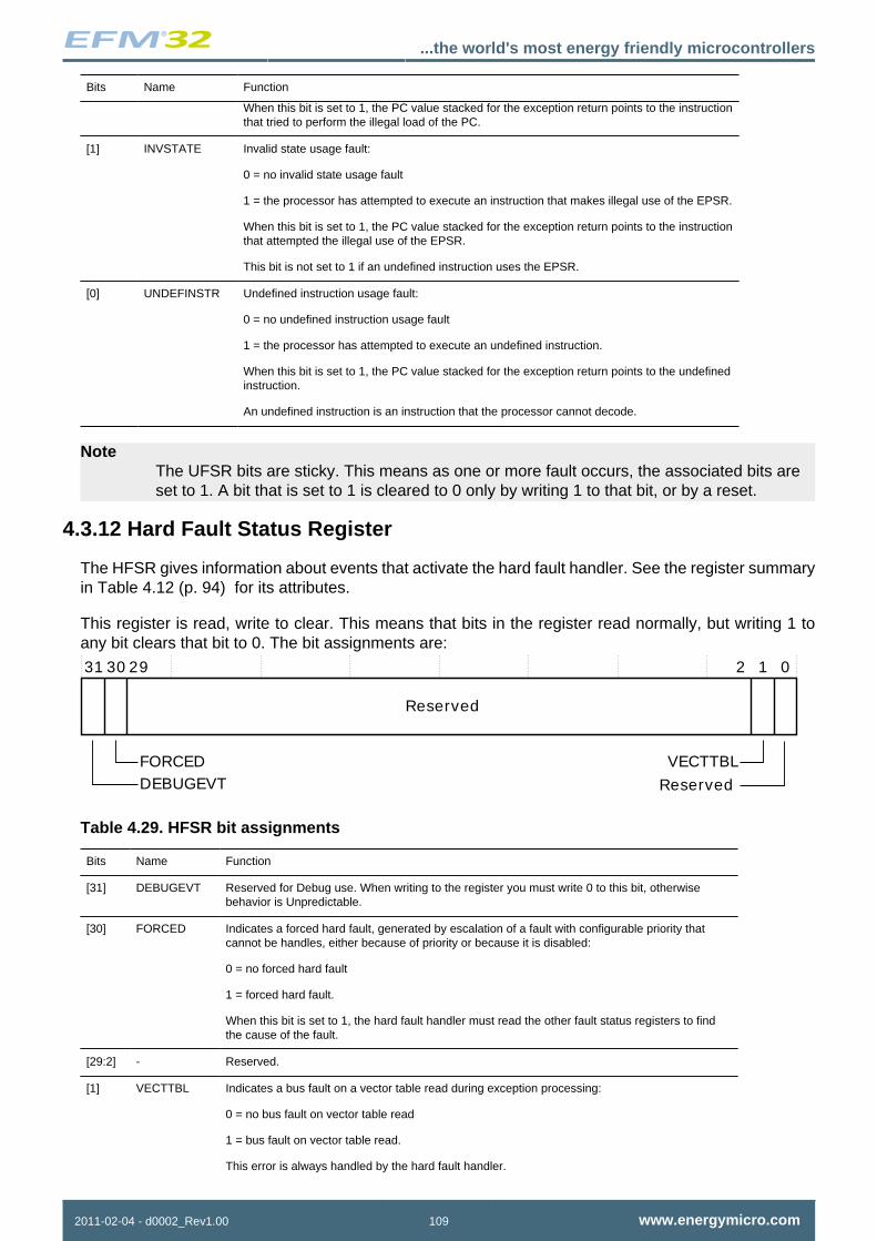
...the world's most energy friendly microcontrollers
2011-02-04 - d0002_Rev1.00 109 www.energymicro.com
Bits Name Function
When this bit is set to 1, the PC value stacked for the exception return points to the instructionthat tried to perform the illegal load of the PC.
[1] INVSTATE Invalid state usage fault:
0 = no invalid state usage fault
1 = the processor has attempted to execute an instruction that makes illegal use of the EPSR.
When this bit is set to 1, the PC value stacked for the exception return points to the instructionthat attempted the illegal use of the EPSR.
This bit is not set to 1 if an undefined instruction uses the EPSR.
[0] UNDEFINSTR Undefined instruction usage fault:
0 = no undefined instruction usage fault
1 = the processor has attempted to execute an undefined instruction.
When this bit is set to 1, the PC value stacked for the exception return points to the undefinedinstruction.
An undefined instruction is an instruction that the processor cannot decode.
NoteThe UFSR bits are sticky. This means as one or more fault occurs, the associated bits areset to 1. A bit that is set to 1 is cleared to 0 only by writing 1 to that bit, or by a reset.
4.3.12 Hard Fault Status Register
The HFSR gives information about events that activate the hard fault handler. See the register summaryin Table 4.12 (p. 94) for its attributes.
This register is read, write to clear. This means that bits in the register read normally, but writing 1 toany bit clears that bit to 0. The bit assignments are:
31 30 2 1 0
Reserved
29
DEBUGEVTFORCED VECTTBL
Reserved
Table 4.29. HFSR bit assignments
Bits Name Function
[31] DEBUGEVT Reserved for Debug use. When writing to the register you must write 0 to this bit, otherwisebehavior is Unpredictable.
[30] FORCED Indicates a forced hard fault, generated by escalation of a fault with configurable priority thatcannot be handles, either because of priority or because it is disabled:
0 = no forced hard fault
1 = forced hard fault.
When this bit is set to 1, the hard fault handler must read the other fault status registers to findthe cause of the fault.
[29:2] - Reserved.
[1] VECTTBL Indicates a bus fault on a vector table read during exception processing:
0 = no bus fault on vector table read
1 = bus fault on vector table read.
This error is always handled by the hard fault handler.

...the world's most energy friendly microcontrollers
2011-02-04 - d0002_Rev1.00 110 www.energymicro.com
Bits Name Function
When this bit is set to 1, the PC value stacked for the exception return points to the instructionthat was preempted by the exception.
[0] - Reserved.
NoteThe HFSR bits are sticky. This means as one or more fault occurs, the associated bits areset to 1. A bit that is set to 1 is cleared to 0 only by writing 1 to that bit, or by a reset.
4.3.13 Memory Management Fault Address Register
The MMFAR contains the address of the location that generated a memory management fault. See theregister summary in Table 4.12 (p. 94) for its attributes. The bit assignments are:
Table 4.30. MMFAR bit assignments
Bits Name Function
[31:0] ADDRESS When the MMARVALID bit of the MMFSR is set to 1, this field holds the address of the locationthat generated the memory management fault
When an unaligned access faults, the address is the actual address that faulted. Because a single reador write instruction can be split into multiple aligned accesses, the fault address can be any address inthe range of the requested access size.
Flags in the MMFSR indicate the cause of the fault, and whether the value in the MMFAR is valid. SeeSection 4.3.11.1 (p. 105) .
4.3.14 Bus Fault Address Register
The BFAR contains the address of the location that generated a bus fault. See the register summary inTable 4.12 (p. 94) for its attributes. The bit assignments are:
Table 4.31. BFAR bit assignments
Bits Name Function
[31:0] ADDRESS When the BFARVALID bit of the BFSR is set to 1, this field holds the address of the location thatgenerated the bus fault
When an unaligned access faults the address in the BFAR is the one requested by the instruction, evenif it is not the address of the fault.
Flags in the BFSR indicate the cause of the fault, and whether the value in the BFAR is valid. SeeSection 4.3.11.2 (p. 107) .
4.3.15 System control block design hints and tips
Ensure software uses aligned accesses of the correct size to access the system control block registers:
• except for the CFSR and SHPR1-SHPR3, it must use aligned word accesses• for the CFSR and SHPR1-SHPR3 it can use byte or aligned halfword or word accesses.
The processor does not support unaligned accesses to system control block registers.
In a fault handler. to determine the true faulting address:
1. Read and save the MMFAR or BFAR value.2. Read the MMARVALID bit in the MMFSR, or the BFARVALID bit in the BFSR. The MMFAR or BFAR
address is valid only if this bit is 1.

...the world's most energy friendly microcontrollers
2011-02-04 - d0002_Rev1.00 111 www.energymicro.com
Software must follow this sequence because another higher priority exception might change the MMFARor BFAR value. For example, if a higher priority handler preempts the current fault handler, the otherfault might change the MMFAR or BFAR value.
4.4 System timer, SysTick
The processor has a 24-bit system timer, SysTick, that counts down from the reload value to zero, reloads(wraps to) the value in the LOAD register on the next clock edge, then counts down on subsequentclocks.
NoteWhen the processor is halted for debugging the counter does not decrement.
The system timer registers are:
Table 4.32. System timer registers summary
Address Name Type Requiredprivilege
Reset value Description
0xE000E010 CTRL RW Privileged 0x00000004 Section 4.4.1 (p. 111)
0xE000E014 LOAD RW Privileged 0x00000000 Section 4.4.2 (p. 112)
0xE000E018 VAL RW Privileged 0x00000000 Section 4.4.3 (p. 112)
0xE000E01C CALIB RO Privileged 0x400036B0 1Section 4.4.4 (p. 113)
1SysTick calibration value.
4.4.1 SysTick Control and Status Register
The SysTick CTRL register enables the SysTick features. See the register summary in Table 4.32 (p.111) for its attributes. The bit assignments are:
0Reserved
31 17 16 15 3 2 1 0
Reserved 0 0
COUNTFLAG CLKSOURCETICKINTENABLE
Table 4.33. SysTick CTRL register bit assignments
Bits Name Function
[31:17] - Reserved.
[16] COUNTFLAG Returns 1 if timer counted to 0 since last time this was read.
[15:3] - Reserved.
[2] CLKSOURCE Indicates the clock source:
0 = Bit 0 of RTC counter value
1 = HFCORECLK
[1] TICKINT Enables SysTick exception request:
0 = counting down to zero does not assert the SysTick exception request
1 = counting down to zero to asserts the SysTick exception request.
Software can use COUNTFLAG to determine if SysTick has ever counted to zero.

...the world's most energy friendly microcontrollers
2011-02-04 - d0002_Rev1.00 112 www.energymicro.com
Bits Name Function
[0] ENABLE Enables the counter:
0 = counter disabled
1 = counter enabled.
When ENABLE is set to 1, the counter loads the RELOAD value from the LOAD register and then countsdown. On reaching 0, it sets the COUNTFLAG to 1 and optionally asserts the SysTick depending on thevalue of TICKINT. It then loads the RELOAD value again, and begins counting.
4.4.2 SysTick Reload Value Register
The LOAD register specifies the start value to load into the VAL register. See the register summary inTable 4.32 (p. 111) for its attributes. The bit assignments are:
31 0
RELOADReserved
2324
Table 4.34. LOAD register bit assignments
Bits Name Function
[31:24] - Reserved.
[23:0] RELOAD Value to load into the VAL register when the counter is enabled and when it reaches 0, seeSection 4.4.2.1 (p. 112) .
4.4.2.1 Calculating the RELOAD value
The RELOAD value can be any value in the range 0x00000001-0x00FFFFFF. A start value of 0 ispossible, but has no effect because the SysTick exception request and COUNTFLAG are activated whencounting from 1 to 0.
The RELOAD value is calculated according to its use:
• To generate a multi-shot timer with a period of N processor clock cycles, use a RELOAD value of N-1.For example, if the SysTick interrupt is required every 100 clock pulses, set RELOAD to 99.
• To deliver a single SysTick interrupt after a delay of N processor clock cycles, use a RELOAD of valueN. For example, if a SysTick interrupt is required after 400 clock pulses, set RELOAD to 400.
4.4.3 SysTick Current Value Register
The VAL register contains the current value of the SysTick counter. See the register summary inTable 4.32 (p. 111) for its attributes. The bit assignments are:
31 0
CURRENTReserved
2324
Table 4.35. VAL register bit assignments
Bits Name Function
[31:24] - Reserved.
[23:0] CURRENT Reads return the current value of the SysTick counter.
A write of any value clears the field to 0, and also clears the SysTick CTRL.COUNTFLAG bit to 0.

...the world's most energy friendly microcontrollers
2011-02-04 - d0002_Rev1.00 113 www.energymicro.com
4.4.4 SysTick Calibration Value Register
The CALIB register indicates the SysTick calibration properties and is a read only register. See theregister summary in Table 4.32 (p. 111) for its attributes. The bit assignments are:
31 0
TENMSReserved
232430
SKEW
NOREF
29
Table 4.36. CALIB register bit assignments
Bits Name Function
[31] NOREF Reads as zero. Indicates that a the RTC counter bit 0 is provided as a reference clock.
[30] SKEW Reads as one. Calibration value for the 10ms inexact timing is not known because TENMS is notknown . This can affect the suitability of SysTick as a software real time clock.
[29:24] - Reserved.
[23:0] TENMS Read as 0x0036B0, which gives 10 ms ticks when running off a 14 MHz clock.
If calibration information is not known, calculate the calibration value required from the frequency of theprocessor clock or external clock.
4.4.5 SysTick design hints and tips
The SysTick counter runs on the processor clock or bit 0 of the RTC counter value. If the clock signal inuse is stopped (e.g. in lower Energy Modes), the SysTick counter stops.
Ensure software uses aligned word accesses to access the SysTick registers.
4.5 Memory protection unit
This section describes the Memory protection unit (MPU).
The MPU divides the memory map into a number of regions, and defines the location, size, accesspermissions, and memory attributes of each region. It supports:
• independent attribute settings for each region• overlapping regions• export of memory attributes to the system.
The memory attributes affect the behavior of memory accesses to the region. The Cortex-M3 MPUdefines:
• eight separate memory regions, 0-7• a background region.
When memory regions overlap, a memory access is affected by the attributes of the region with thehighest number. For example, the attributes for region 7 take precedence over the attributes of anyregion that overlaps region 7.
The background region has the same memory access attributes as the default memory map, but isaccessible from privileged software only.

...the world's most energy friendly microcontrollers
2011-02-04 - d0002_Rev1.00 114 www.energymicro.com
The Cortex-M3 MPU memory map is unified. This means instruction accesses and data accesses havesame region settings.
If a program accesses a memory location that is prohibited by the MPU, the processor generates amemory management fault. This causes a fault exception, and might cause termination of the processin an OS environment. In an OS environment, the kernel can update the MPU region setting dynamicallybased on the process to be executed. Typically, an embedded OS uses the MPU for memory protection.
Configuration of MPU regions is based on memory types, see Section 2.2.1 (p. 15) .
Table 4.37 (p. 114) shows the possible MPU region attributes. Please not that the Shareabilityand cache behavior attributes are usually not relevant for the EFM32 devices since these are notused by other bus masters. However, these can be useful together with the DMA Controller. SeeSection 4.5.9.1 (p. 123) for guidelines on using these attributes.
Table 4.37. Memory attributes summary
Memorytype
Shareability Other attributes Description
Strongly-ordered
- - All accesses to Strongly-ordered memory occur in programorder. All Strongly-ordered regions are assumed to be shared.
Device Shared - Memory-mapped peripherals that several processors share.
Non-shared - Memory-mapped peripherals that only a single processor uses.
Normal Shared Non-cacheable Write-through Cacheable Write-back Cacheable
Normal memory that is shared between several processors.
Non-shared Non-cacheable Write-through Cacheable Write-back Cacheable
Normal memory that only a single processor uses.
Use the MPU registers to define the MPU regions and their attributes. The MPU registers are:
Table 4.38. MPU registers summary
Address Name Type Requiredprivilege
Reset value Description
0xE000ED90 TYPE RO Privileged 0x00000800 Section 4.5.1 (p. 114)
0xE000ED94 CTRL RW Privileged 0x00000000 Section 4.5.2 (p. 115)
0xE000ED98 RNR RW Privileged 0x00000000 Section 4.5.3 (p. 116)
0xE000ED9C RBAR RW Privileged 0x00000000 Section 4.5.4 (p. 117)
0xE000EDA0 RASR RW Privileged 0x00000000 Section 4.5.5 (p. 117)
0xE000EDA4 RBAR_A1 RW Privileged 0x00000000 Alias of RBAR, see Section 4.5.4 (p. 117)
0xE000EDA8 RASR_A1 RW Privileged 0x00000000 Alias of RASR, see Section 4.5.5 (p. 117)
0xE000EDAC RBAR_A2 RW Privileged 0x00000000 Alias of RBAR, see Section 4.5.4 (p. 117)
0xE000EDB0 RASR_A2 RW Privileged 0x00000000 Alias of RASR, see Section 4.5.5 (p. 117)
0xE000EDB4 RBAR_A3 RW Privileged 0x00000000 Alias of RBAR, see Section 4.5.4 (p. 117)
0xE000EDB8 RASR_A3 RW Privileged 0x00000000 Alias of RASR, see Section 4.5.5 (p. 117)
4.5.1 MPU Type Register
The TYPE register indicates how many regions the MPU supports. See the register summary inTable 4.38 (p. 114) for its attributes. The bit assignments are:

...the world's most energy friendly microcontrollers
2011-02-04 - d0002_Rev1.00 115 www.energymicro.com
Reserved
31 24 23 16 15 8 7 1 0
IREGION DREGION Reserved
SEPARATE
Table 4.39. TYPE register bit assignments
Bits Name Function
[31:24] - Reserved.
[23:16] IREGION Indicates the number of supported MPU instruction regions.
Always contains 0x00. The MPU memory map is unified and is described by the DREGION field.
[15:8] DREGION Indicates the number of supported MPU data regions:
0x08 = Eight MPU regions.
[7:0] - Reserved.
[0] SEPARATE Indicates support for unified or separate instruction and date memory maps:
0 = unified.
4.5.2 MPU Control Register
The MPU CTRL register:
• enables the MPU• enables the default memory map background region• enables use of the MPU when in the hard fault, Non-maskable Interrupt (NMI), and FAULTMASK
escalated handlers.
See the register summary in Table 4.38 (p. 114) for the MPU CTRL attributes. The bit assignments are:
31 1 0
Reserved
HFNMIENAENABLE
2
PRIVDEFENA
3
Table 4.40. MPU CTRL register bit assignments
Bits Name Function
[31:3] - Reserved.
[2] PRIVDEFENA Enables privileged software access to the default memory map:
0 = If the MPU is enabled, disables use of the default memory map. Any memory access to alocation not covered by any enabled region causes a fault.
1 = If the MPU is enabled, enables use of the default memory map as a background region forprivileged software accesses.
When enabled, the background region acts as if it is region number -1. Any region that isdefined and enabled has priority over this default map.
If the MPU is disabled, the processor ignores this bit.
[1] HFNMIENA Enables the operation of MPU during hard fault, NMI, and FAULTMASK handlers.
When the MPU is enabled:

...the world's most energy friendly microcontrollers
2011-02-04 - d0002_Rev1.00 116 www.energymicro.com
Bits Name Function
0 = MPU is disabled during hard fault, NMI, and FAULTMASK handlers, regardless of the valueof the ENABLE bit
1 = the MPU is enabled during hard fault, NMI, and FAULTMASK handlers.
When the MPU is disabled, if this bit is set to 1 the behavior is Unpredictable.
[0] ENABLE Enables the MPU:
0 = MPU disabled
1 = MPU enabled.
When ENABLE and PRIVDEFENA are both set to 1:
• For privileged accesses, the default memory map is as described in Section 2.2 (p. 14) . Any accessby privileged software that does not address an enabled memory region behaves as defined by thedefault memory map.
• Any access by unprivileged software that does not address an enabled memory region causes amemory management fault.
XN and Strongly-ordered rules always apply to the System Control Space regardless of the value ofthe ENABLE bit.
When the ENABLE bit is set to 1, at least one region of the memory map must be enabled for the systemto function unless the PRIVDEFENA bit is set to 1. If the PRIVDEFENA bit is set to 1 and no regionsare enabled, then only privileged software can operate.
When the ENABLE bit is set to 0, the system uses the default memory map. This has the same memoryattributes as if the MPU is not implemented, see Table 2.11 (p. 16) . The default memory map appliesto accesses from both privileged and unprivileged software.
When the MPU is enabled, accesses to the System Control Space and vector table are always permitted.Other areas are accessible based on regions and whether PRIVDEFENA is set to 1.
Unless HFNMIENA is set to 1, the MPU is not enabled when the processor is executing the handler foran exception with priority –1 or –2. These priorities are only possible when handling a hard fault or NMIexception, or when FAULTMASK is enabled. Setting the HFNMIENA bit to 1 enables the MPU whenoperating with these two priorities.
4.5.3 MPU Region Number Register
The RNR selects which memory region is referenced by the RBAR and RASR registers. See the registersummary in Table 4.38 (p. 114) for its attributes. The bit assignments are:
Reserved
31 8 7 0
REGION
Table 4.41. RNR bit assignments
Bits Name Function
[31:8] - Reserved.
[7:0] REGION Indicates the MPU region referenced by the RBAR and RASR registers.
The MPU supports 8 memory regions, so the permitted values of this field are 0-7.
Normally, you write the required region number to this register before accessing the RBAR or RASR.However you can change the region number by writing to the RBAR with the VALID bit set to 1, seeSection 4.5.4 (p. 117) . This write updates the value of the REGION field.

...the world's most energy friendly microcontrollers
2011-02-04 - d0002_Rev1.00 117 www.energymicro.com
4.5.4 MPU Region Base Address Register
The RBAR defines the base address of the MPU region selected by the RNR, and can update the valueof the RNR. See the register summary in Table 4.38 (p. 114) for its attributes.
Write RBAR with the VALID bit set to 1 to change the current region number and update the RNR. Thebit assignments are:
VALID
ADDR
31 N N-1 5 4 3 0
Reserved REGION
If the region size is 32B, the ADDR field is bits [31:5] and there is no Reserved field
Table 4.42. RBAR bit assignments
Bits Name Function
[31:N] ADDR Region base address field. The value of N depends on the region size. For more information seeSection 4.5.4.1 (p. 117) .
[(N-1):5] - Reserved.
[4] VALID MPU Region Number valid bit:
Write:
0 = RNR not changed, and the processor:
• updates the base address for the region specified in the RNR• ignores the value of the REGION field
1 = the processor:
• updates the value of the RNR to the value of the REGION field• updates the base address for the region specified in the REGION field.
Always reads as zero.
[3:0] REGION MPU region field:
For the behavior on writes, see the description of the VALID field.
On reads, returns the current region number, as specified by the RNR.
4.5.4.1 The ADDR field
The ADDR field is bits[31:N] of the RBAR. The region size, as specified by the SIZE field in the RASR,defines the value of N:
N = Log2(Region size in bytes),
If the region size is configured to 4GB, in the RASR, there is no valid ADDR field. In this case, the regionoccupies the complete memory map, and the base address is 0x00000000.
The base address is aligned to the size of the region. For example, a 64KB region must be aligned ona multiple of 64KB, for example, at 0x00010000 or 0x00020000.
4.5.5 MPU Region Attribute and Size Register
The RASR defines the region size and memory attributes of the MPU region specified by the RNR,and enables that region and any subregions. See the register summary in Table 4.38 (p. 114) forits attributes.

...the world's most energy friendly microcontrollers
2011-02-04 - d0002_Rev1.00 118 www.energymicro.com
RASR is accessible using word or halfword accesses:
• the most significant halfword holds the region attributes• the least significant halfword holds the region size and the region and subregion enable bits.
The bit assignments are:
XNReserved
31 29 28 27 26 24 23 22 21 19 18 17 16 15 8 7 6 5 1 0
AP TEX S C B SRD SIZE
ENABLEReserved
Reserved
Reserved
Table 4.43. RASR bit assignments
Bits Name Function
[31:29] - Reserved.
[28] XN Instruction access disable bit:
0 = instruction fetches enabled1 = instruction fetches disabled.
[27] - Reserved.
[26:24] AP Access permission field, see Table 4.47 (p. 120) .
[23:22] - Reserved.
[21:19, 17, 16] TEX, C, B Memory access attributes, see Table 4.45 (p. 119) .
[18] S Shareable bit, see Table 4.45 (p. 119) .
[15:8] SRD Subregion disable bits. For each bit in this field:
0 = corresponding sub-region is enabled
1 = corresponding sub-region is disabled
See Section 4.5.8.3 (p. 122) for more information.
Region sizes of 128 bytes and less do not support subregions. When writing the attributesfor such a region, write the SRD field as 0x00.
[7:6] - Reserved.
[5:1] SIZE Specifies the size of the MPU protection region. The minimum permitted value is 3(b00010), see See Section 4.5.5.1 (p. 118) for more information.
[0] ENABLE Region enable bit.
For information about access permission, see Section 4.5.6 (p. 119) .
4.5.5.1 SIZE field values
The SIZE field defines the size of the MPU memory region specified by the RNR. as follows:
(Region size in bytes) = 2(SIZE+1)
The smallest permitted region size is 32B, corresponding to a SIZE value of 4. Table 4.44 (p. 118)gives example SIZE values, with the corresponding region size and value of N in the RBAR.
Table 4.44. Example SIZE field values
SIZE value Region size Value of N 1 Note
b00100 (4) 32B 5 Minimum permitted size

...the world's most energy friendly microcontrollers
2011-02-04 - d0002_Rev1.00 119 www.energymicro.com
SIZE value Region size Value of N 1 Note
b01001 (9) 1KB 10 -
b10011 (19) 1MB 20 -
b11101 (29) 1GB 30 -
b11111 (31) 4GB b01100 Maximum possible size
1In the RBAR, see Section 4.5.4 (p. 117) .
4.5.6 MPU access permission attributes
This section describes the MPU access permission attributes. The access permission bits, TEX, C, B,S, AP, and XN, of the RASR, control access to the corresponding memory region. If an access is madeto an area of memory without the required permissions, then the MPU generates a permission fault.
Table 4.45 (p. 119) shows the encodings for the TEX, C, B, and S access permission bits.
Table 4.45. TEX, C, B, and S encoding
TEX C B S Memory type Shareability Other attributes
0 x 1 Strongly-ordered Shareable -0
1 x 1 Device Shareable -
0 Not shareable0
1
Normal
Shareable
Outer and inner write-through. No write allocate.
0 Not shareable
b000
1
1
1
Normal
Shareable
Outer and inner write-back. No write allocate.
0 Not shareable0
1
Normal
Shareable
Outer and inner noncacheable.0
1 x 1 Reserved encoding -
0 x 1 Implementation defined attributes. -
0 Not shareable
b001
1
1
1
Normal
Shareable
Outer and inner write-back. Write and read allocate.
0 x 1 Device Not shareable Nonshared Device.0
1 x 1 Reserved encoding -
b010
1 x 1 x 1 Reserved encoding -
0 Not shareableb1BB A A
1
Normal
Shareable
Cached memory 2, BB = outer policy, AA = inner policy.
1The MPU ignores the value of this bit.2See Table 4.46 (p. 119) for the encoding of the AA and BB bits.
Table 4.46 (p. 119) shows the cache policy for memory attribute encodings with a TEX value is inthe range 4-7.
Table 4.46. Cache policy for memory attribute encoding
Encoding, AA or BB Corresponding cache policy
00 Non-cacheable
01 Write back, write and read allocate
10 Write through, no write allocate
11 Write back, no write allocate
...the world's most energy friendly microcontrollers
2011-02-04 - d0002_Rev1.00 120 www.energymicro.com
Table 4.47 (p. 120) shows the AP encodings that define the access permissions for privileged andunprivileged software.
Table 4.47. AP encoding
AP[2:0] Privileged
permissions
Unprivileged
permissions
Description
000 No access No access All accesses generate a permission fault
001 RW No access Access from privileged software only
010 RW RO Writes by unprivileged software generate a permission fault
011 RW RW Full access
100 Unpredictable Unpredictable Reserved
101 RO No access Reads by privileged software only
110 RO RO Read only, by privileged or unprivileged software
111 RO RO Read only, by privileged or unprivileged software
4.5.7 MPU mismatch
When an access violates the MPU permissions, the processor generates a memory management fault,see Section 2.1.4 (p. 13) . The MMFSR indicates the cause of the fault. See Section 4.3.11.1 (p. 105)for more information.
4.5.8 Updating an MPU region
To update the attributes for an MPU region, update the RNR, RBAR and RASR registers. You canprogram each register separately, or use a multiple-word write to program all of these registers. You canuse the RBAR and RASR aliases to program up to four regions simultaneously using an STM instruction.
4.5.8.1 Updating an MPU region using separate words
Simple code to configure one region:
; R1 = region number
; R2 = size/enable
; R3 = attributes
; R4 = address
LDR R0,=MPU_RNR ; 0xE000ED98, MPU region number register
STR R1, [R0, #0x0] ; Region Number
STR R4, [R0, #0x4] ; Region Base Address
STRH R2, [R0, #0x8] ; Region Size and Enable
STRH R3, [R0, #0xA] ; Region Attribute
Disable a region before writing new region settings to the MPU if you have previously enabled the regionbeing changed. For example:

...the world's most energy friendly microcontrollers
2011-02-04 - d0002_Rev1.00 121 www.energymicro.com
; R1 = region number
; R2 = size/enable
; R3 = attributes
; R4 = address
LDR R0,=MPU_RNR ; 0xE000ED98, MPU region number register
STR R1, [R0, #0x0] ; Region Number
BIC R2, R2, #1 ; Disable
STRH R2, [R0, #0x8] ; Region Size and Enable
STR R4, [R0, #0x4] ; Region Base Address
STRH R3, [R0, #0xA] ; Region Attribute
ORR R2, #1 ; Enable
STRH R2, [R0, #0x8] ; Region Size and Enable
Software must use memory barrier instructions:
• before MPU setup if there might be outstanding memory transfers, such as buffered writes, that mightbe affected by the change in MPU settings
• after MPU setup if it includes memory transfers that must use the new MPU settings.
However, memory barrier instructions are not required if the MPU setup process starts by entering anexception handler, or is followed by an exception return, because the exception entry and exceptionreturn mechanism cause memory barrier behavior.
Software does not need any memory barrier instructions during MPU setup, because it accesses theMPU through the PPB, which is a Strongly-Ordered memory region.
For example, if you want all of the memory access behavior to take effect immediately after theprogramming sequence, use a DSB instruction and an ISB instruction. A DSB is required after changingMPU settings, such as at the end of context switch. An ISB is required if the code that programs theMPU region or regions is entered using a branch or call. If the programming sequence is entered usinga return from exception, or by taking an exception, then you do not require an ISB.
4.5.8.2 Updating an MPU region using multi-word writes
You can program directly using multi-word writes, depending on how the information is divided. Considerthe following reprogramming:
; R1 = region number
; R2 = address

...the world's most energy friendly microcontrollers
2011-02-04 - d0002_Rev1.00 122 www.energymicro.com
; R3 = size, attributes in one
LDR R0, =MPU_RNR ; 0xE000ED98, MPU region number register
STR R1, [R0, #0x0] ; Region Number
STR R2, [R0, #0x4] ; Region Base Address
STR R3, [R0, #0x8] ; Region Attribute, Size and Enable
Use an STM instruction to optimize this:
; R1 = region number
; R2 = address
; R3 = size, attributes in one
LDR R0, =MPU_RNR ; 0xE000ED98, MPU region number register
STM R0, {R1-R3} ; Region Number, address, attribute, size and enable
You can do this in two words for pre-packed information. This means that the RBAR contains the requiredregion number and had the VALID bit set to 1, see Section 4.5.4 (p. 117) . Use this when the data isstatically packed, for example in a boot loader:
; R1 = address and region number in one
; R2 = size and attributes in one
LDR R0, =MPU_RBAR ; 0xE000ED9C, MPU Region Base register
STR R1, [R0, #0x0] ; Region base address and ; region number combined with VALID (bit 4) set to 1
STR R2, [R0, #0x4] ; Region Attribute, Size and Enable
Use an STM instruction to optimize this:
; R1 = address and region number in one
; R2 = size and attributes in one
LDR R0,=MPU_RBAR ; 0xE000ED9C, MPU Region Base register
STM R0, {R1-R2} ; Region base address, region number and VALID bit, ; and Region Attribute, Size and Enable
4.5.8.3 Subregions
Regions of 256 bytes or more are divided into eight equal-sized subregions. Set the corresponding bitin the SRD field of the RASR to disable a subregion, see Section 4.5.5 (p. 117) . The least significant

...the world's most energy friendly microcontrollers
2011-02-04 - d0002_Rev1.00 123 www.energymicro.com
bit of SRD controls the first subregion, and the most significant bit controls the last subregion. Disablinga subregion means another region overlapping the disabled range matches instead. If no other enabledregion overlaps the disabled subregion the MPU issues a fault.
Regions of 32, 64, and 128 bytes do not support subregions, With regions of these sizes, you must setthe SRD field to 0x00, otherwise the MPU behavior is Unpredictable.
4.5.8.3.1 Example of SRD use
Two regions with the same base address overlap. Region one is 128KB, and region two is 512KB. Toensure the attributes from region one apply to the first128KB region, set the SRD field for region two tob00000011 to disable the first two subregions, as the figure shows.
Region 1
Disabled subregion
Disabled subregion
Region 2, with subregions
Base address of both regions
Offset frombase address
064KB
128KB192KB256KB320KB384KB448KB512KB
4.5.9 MPU design hints and tips
To avoid unexpected behavior, disable the interrupts before updating the attributes of a region that theinterrupt handlers might access.
Ensure software uses aligned accesses of the correct size to access MPU registers:
• except for the RASR, it must use aligned word accesses• for the RASR it can use byte or aligned halfword or word accesses.
The processor does not support unaligned accesses to MPU registers.
When setting up the MPU, and if the MPU has previously been programmed, disable unused regions toprevent any previous region settings from affecting the new MPU setup.
4.5.9.1 MPU configuration for a microcontroller
The EFM32 devices has only a single processor and information on Shareability and cache behavior isnot used. In such a system, program the MPU as follows:
Table 4.48. Memory region attributes for a microcontroller
Memory region TEX C B S Memory type and attributes
Flash memory b000 1 0 0 Normal memory, Non-shareable, write-through
Internal SRAM b000 1 0 1 Normal memory, Shareable, write-through
External SRAM b000 1 1 1 Normal memory, Shareable, write-back, write-allocate
Peripherals b000 0 1 1 Device memory, Shareable
In the EFM32 devices the shareability and cache policy attributes do not affect the system behavior.However, using these settings for the MPU regions can make the application code more portable andalso be useful for setups with the DMA Controller. The values given are for typical situations.

...the world's most energy friendly microcontrollers
2011-02-04 - d0002_Rev1.00 124 www.energymicro.com
GlossaryThis glossary describes some of the terms used in technical documents from ARM.
Abort A mechanism that indicates to a processor that the value associated with amemory access is invalid. An abort can be caused by the external or internalmemory system as a result of attempting to access invalid instruction or datamemory.
Aligned A data item stored at an address that is divisible by the number of bytes thatdefines the data size is said to be aligned. Aligned words and halfwords haveaddresses that are divisible by four and two respectively. The terms word-aligned and halfword-aligned therefore stipulate addresses that are divisibleby four and two respectively.
Banked register A register that has multiple physical copies, where the state of the processordetermines which copy is used. The Stack Pointer, SP (R13) is a bankedregister.
Base register In instruction descriptions, a register specified by a load or store instructionthat is used to hold the base value for the instruction’s address calculation.Depending on the instruction and its addressing mode, an offset can beadded to or subtracted from the base register value to form the address thatis sent to memory.See Also Index register.
Big-endian (BE) Byte ordering scheme in which bytes of decreasing significance in a dataword are stored at increasing addresses in memory.See Also Byte-invariant, Endianness, Little-endian.
Big-endian memory Memory in which:
• a byte or halfword at a word-aligned address is the most significant byteor halfword within the word at that address
• a byte at a halfword-aligned address is the most significant byte within thehalfword at that address.
See Also Little-endian memory.
Breakpoint A breakpoint is a mechanism provided by debuggers to identify an instructionat which program execution is to be halted. Breakpoints are inserted by theprogrammer to enable inspection of register contents, memory locations,variable values at fixed points in the program execution to test that theprogram is operating correctly. Breakpoints are removed after the programis successfully tested.
Byte-invariant In a byte-invariant system, the address of each byte of memory remainsunchanged when switching between little-endian and big-endian operation.When a data item larger than a byte is loaded from or stored to memory,the bytes making up that data item are arranged into the correct orderdepending on the endianness of the memory access. An ARM byte-invariant implementation also supports unaligned halfword and word memoryaccesses. It expects multi-word accesses to be word-aligned.
Cache A block of on-chip or off-chip fast access memory locations, situated betweenthe processor and main memory, used for storing and retrieving copies ofoften used instructions, data, or instructions and data. This is done to greatly

...the world's most energy friendly microcontrollers
2011-02-04 - d0002_Rev1.00 125 www.energymicro.com
increase the average speed of memory accesses and so improve processorperformance.
Condition field A four-bit field in an instruction that specifies a condition under which theinstruction can execute.
Conditional execution If the condition code flags indicate that the corresponding condition is truewhen the instruction starts executing, it executes normally. Otherwise, theinstruction does nothing.
Context The environment that each process operates in for a multitasking operatingsystem. In ARM processors, this is limited to mean the physical addressrange that it can access in memory and the associated memory accesspermissions.
Coprocessor A processor that supplements the main processor. Cortex-M3 does notsupport any coprocessors.
Debugger A debugging system that includes a program, used to detect, locate, andcorrect software faults, together with custom hardware that supports softwaredebugging.
Direct Memory Access(DMA)
An operation that accesses main memory directly, without the processorperforming any accesses to the data concerned.
Doubleword A 64-bit data item. The contents are taken as being an unsigned integerunless otherwise stated.
Doubleword-aligned A data item having a memory address that is divisible by eight.
Endianness Byte ordering. The scheme that determines the order that successive bytesof a data word are stored in memory. An aspect of the system’s memorymapping.See Also Little-endian and Big-endian.
Exception An event that interrupts program execution. When an exception occurs,the processor suspends the normal program flow and starts execution atthe address indicated by the corresponding exception vector. The indicatedaddress contains the first instruction of the handler for the exception.
An exception can be an interrupt request, a fault, or a software-generatedsystem exception. Faults include attempting an invalid memory access,attempting to execute an instruction in an invalid processor state, andattempting to execute an undefined instruction.
Exception service routine See Interrupt handler.
Exception vector See Interrupt vector.
Flat address mapping A system of organizing memory in which each physical address in thememory space is the same as the corresponding virtual address.
Halfword A 16-bit data item.
Illegal instruction An instruction that is architecturally Undefined.
Implementation-defined The behavior is not architecturally defined, but is defined and documentedby individual implementations.

...the world's most energy friendly microcontrollers
2011-02-04 - d0002_Rev1.00 126 www.energymicro.com
Implementation-specific The behavior is not architecturally defined, and does not have to bedocumented by individual implementations. Used when there are a numberof implementation options available and the option chosen does not affectsoftware compatibility.
Index register In some load and store instruction descriptions, the value of this registeris used as an offset to be added to or subtracted from the base registervalue to form the address that is sent to memory. Some addressing modesoptionally enable the index register value to be shifted prior to the additionor subtraction.See Also Base register.
Instruction cycle count The number of cycles that an instruction occupies the Execute stage of thepipeline.
Interrupt handler A program that control of the processor is passed to when an interrupt occurs.
Interrupt vector One of a number of fixed addresses in low memory, or in high memory if highvectors are configured, that contains the first instruction of the correspondinginterrupt handler.
Little-endian (LE) Byte ordering scheme in which bytes of increasing significance in a data wordare stored at increasing addresses in memory.See Also Big-endian, Byte-invariant, Endianness.
Little-endian memory Memory in which:
• a byte or halfword at a word-aligned address is the least significant byteor halfword within the word at that address
• a byte at a halfword-aligned address is the least significant byte within thehalfword at that address.
See Also Big-endian memory.
Load/store architecture A processor architecture where data-processing operations only operate onregister contents, not directly on memory contents.
Memory Protection Unit(MPU)
Hardware that controls access permissions to blocks of memory. An MPUdoes not perform any address translation.
Prefetching In pipelined processors, the process of fetching instructions from memory tofill up the pipeline before the preceding instructions have finished executing.Prefetching an instruction does not mean that the instruction has to beexecuted.
Read Reads are defined as memory operations that have the semantics of aload. Reads include the Thumb instructions LDM, LDR, LDRSH, LDRH, LDRSB,LDRB, and POP.
Region A partition of memory space.
Reserved A field in a control register or instruction format is reserved if the field is tobe defined by the implementation, or produces Unpredictable results if thecontents of the field are not zero. These fields are reserved for use in futureextensions of the architecture or are implementation#specific. All reservedbits not used by the implementation must be written as 0 and read as 0.
Should Be One (SBO) Write as 1, or all 1s for bit fields, by software. Writing as 0 producesUnpredictable results.

...the world's most energy friendly microcontrollers
2011-02-04 - d0002_Rev1.00 127 www.energymicro.com
Should Be Zero (SBZ) Write as 0, or all 0s for bit fields, by software. Writing as 1 producesUnpredictable results.
Should Be Zero orPreserved (SBZP)
Write as 0, or all 0s for bit fields, by software, or preserved by writing thesame value back that has been previously read from the same field on thesame processor.
Thread-safe In a multi-tasking environment, thread-safe functions use safeguardmechanisms when accessing shared resources, to ensure correct operationwithout the risk of shared access conflicts.
Thumb instruction One or two halfwords that specify an operation for a processor to perform.Thumb instructions must be halfword-aligned.
Unaligned A data item stored at an address that is not divisible by the number of bytesthat defines the data size is said to be unaligned. For example, a word storedat an address that is not divisible by four.
Undefined Indicates an instruction that generates an Undefined instruction exception.
Unpredictable (UNP) You cannot rely on the behavior. Unpredictable behavior must not representsecurity holes. Unpredictable behavior must not halt or hang the processor,or any parts of the system.
Warm reset Also known as a core reset. Initializes the majority of the processor excludingthe debug controller and debug logic. This type of reset is useful if you areusing the debugging features of a processor.
WA See Write-allocate.
WB See Write-back.
Word A 32-bit data item.
Write Writes are defined as operations that have the semantics of a store. Writesinclude the Thumb instructions STM, STR, STRH, STRB, and PUSH.
Write-allocate (WA) In a write-allocate cache, a cache miss on storing data causes a cache lineto be allocated into the cache.
Write-back (WB) In a write-back cache, data is only written to main memory when it is forcedout of the cache on line replacement following a cache miss. Otherwise,writes by the processor only update the cache. This is also known ascopyback.
Write buffer A block of high-speed memory, arranged as a FIFO buffer, between thedata cache and main memory, whose purpose is to optimize stores to mainmemory.
Write-through (WT) In a write-through cache, data is written to main memory at the same timeas the cache is updated.
...the world's most energy friendly microcontrollers
2011-02-04 - d0002_Rev1.00 128 www.energymicro.com
5 Revision History
5.1 Revision 1.00
February 4th, 2011
Updated document to reflect all EFM32 ARM Cortex-M3 devices.
Added information on differences between EFM32G, EFM32GG and EFM32TG devices.
5.2 Revision 0.81
December 9th, 2009
Corrected intrinsic function for Wait For Interrupt in 2.5.4
Added description of all PRIGROUP settings in Table 4-18
5.3 Revision 0.80
Initial preliminary revision, October 19th, 2009

...the world's most energy friendly microcontrollers
2011-02-04 - d0002_Rev1.00 129 www.energymicro.com
A Disclaimer and Trademarks
A.1 Disclaimer
Energy Micro AS intends to provide customers with the latest, accurate, and in-depth documentationof all peripherals and modules available for system and software implementers using or intending touse the Energy Micro products. Characterization data, available modules and peripherals, memorysizes and memory addresses refer to each specific device, and "Typical" parameters provided can anddo vary in different applications. Application examples described herein are for illustrative purposesonly. Energy Micro reserves the right to make changes without further notice and limitation to productinformation, specifications, and descriptions herein, and does not give warranties as to the accuracyor completeness of the included information. Energy Micro shall have no liability for the consequencesof use of the information supplied herein. This document does not imply or express copyright licensesgranted hereunder to design or fabricate any integrated circuits. The products must not be used withinany Life Support System without the specific written consent of Energy Micro. A "Life Support System"is any product or system intended to support or sustain life and/or health, which, if it fails, can bereasonably expected to result in significant personal injury or death. Energy Micro products are generallynot intended for military applications. Energy Micro products shall under no circumstances be used inweapons of mass destruction including (but not limited to) nuclear, biological or chemical weapons, ormissiles capable of delivering such weapons.
A.2 Trademark Information
Energy Micro, EFM32, EFR, logo and combinations thereof, and others are the registered trademarks ortrademarks of Energy Micro AS. ARM, CORTEX, THUMB are the registered trademarks of ARM Limited.Other terms and product names may be trademarks of others.

...the world's most energy friendly microcontrollers
2011-02-04 - d0002_Rev1.00 130 www.energymicro.com
B Contact Information
B.1 Energy Micro Corporate Headquarters
Postal Address Visitor Address Technical Support
Energy Micro ASP.O. Box 4633 NydalenN-0405 OsloNORWAY
Energy Micro ASSandakerveien 118N-0484 OsloNORWAY
support.energymicro.comPhone: +47 40 10 03 01
www.energymicro.comPhone: +47 23 00 98 00Fax: + 47 23 00 98 01
B.2 Global Contacts
Visit www.energymicro.com for information on global distributors and representatives or [email protected] for additional information.
Americas Europe, Middle East and Africa Asia and Pacific
www.energymicro.com/americas www.energymicro.com/emea www.energymicro.com/asia

...the world's most energy friendly microcontrollers
2011-02-04 - d0002_Rev1.00 131 www.energymicro.com
Table of Contents1. Introduction .............................................................................................................................................. 2
1.1. About this document ....................................................................................................................... 21.2. About the EFM32 Cortex-M3 processor and core peripherals .................................................................. 2
2. The Cortex-M3 Processor ........................................................................................................................... 62.1. Programmers model ........................................................................................................................ 62.2. Memory model .............................................................................................................................. 142.3. Exception model ........................................................................................................................... 222.4. Fault handling .............................................................................................................................. 282.5. Power management ....................................................................................................................... 30
3. The Cortex-M3 Instruction Set ................................................................................................................... 333.1. Instruction set summary ................................................................................................................. 333.2. Intrinsic functions .......................................................................................................................... 373.3. About the instruction descriptions ..................................................................................................... 383.4. Memory access instructions ............................................................................................................ 453.5. General data processing instructions ................................................................................................ 563.6. Multiply and divide instructions ........................................................................................................ 663.7. Saturating instructions .................................................................................................................... 693.8. Bitfield instructions ........................................................................................................................ 713.9. Branch and control instructions ........................................................................................................ 733.10. Miscellaneous instructions ............................................................................................................. 79
4. The Cortex-M3 Peripherals ........................................................................................................................ 884.1. About the peripherals ..................................................................................................................... 884.2. Nested Vectored Interrupt Controller ................................................................................................. 884.3. System control block ..................................................................................................................... 944.4. System timer, SysTick .................................................................................................................. 1114.5. Memory protection unit ................................................................................................................. 113
Glossary .................................................................................................................................................. 1245. Revision History ..................................................................................................................................... 128
5.1. Revision 1.00 .............................................................................................................................. 1285.2. Revision 0.81 .............................................................................................................................. 1285.3. Revision 0.80 .............................................................................................................................. 128
A. Disclaimer and Trademarks ..................................................................................................................... 129A.1. Disclaimer .................................................................................................................................. 129A.2. Trademark Information ................................................................................................................. 129
B. Contact Information ................................................................................................................................ 130B.1. Energy Micro Corporate Headquarters ............................................................................................ 130B.2. Global Contacts .......................................................................................................................... 130

...the world's most energy friendly microcontrollers
2011-02-04 - d0002_Rev1.00 132 www.energymicro.com
List of Figures1.1. EFM32 Cortex-M3 implementation ............................................................................................................. 32.1. Bit-band mapping ................................................................................................................................. 192.2. Vector table ......................................................................................................................................... 253.1. ASR #3 ............................................................................................................................................... 403.2. LSR #3 ............................................................................................................................................... 413.3. LSL #3 ................................................................................................................................................ 413.4. ROR #3 .............................................................................................................................................. 423.5. RRX ................................................................................................................................................... 42

...the world's most energy friendly microcontrollers
2011-02-04 - d0002_Rev1.00 133 www.energymicro.com
List of Tables1.1. Cortex-M3 configuration in EFM32 series .................................................................................................... 52.1. Summary of processor mode, execution privilege level, and stack use options .................................................... 62.2. Core register set summary ....................................................................................................................... 72.3. PSR register combinations ....................................................................................................................... 92.4. APSR bit assignments ............................................................................................................................. 92.5. IPSR bit assignments ............................................................................................................................ 102.6. EPSR bit assignments ........................................................................................................................... 102.7. PRIMASK register bit assignments ........................................................................................................... 112.8. FAULTMASK register bit assignments ....................................................................................................... 122.9. BASEPRI register bit assignments ............................................................................................................ 122.10. CONTROL register bit assignments ........................................................................................................ 132.11. Memory access behavior ...................................................................................................................... 162.12. SRAM memory bit-banding regions ......................................................................................................... 182.13. Peripheral memory bit-banding regions .................................................................................................... 182.14. C compiler intrinsic functions for exclusive access instructions ..................................................................... 212.15. Properties of the different exception types ................................................................................................ 232.16. Exception return behavior ..................................................................................................................... 282.17. Faults ................................................................................................................................................ 282.18. Fault status and fault address registers ................................................................................................... 303.1. Cortex-M3 instructions ........................................................................................................................... 333.2. CMSIS intrinsic functions to generate some Cortex-M3 instructions ................................................................ 373.3. CMSIS intrinsic functions to access the special registers .............................................................................. 373.4. Condition code suffixes .......................................................................................................................... 443.5. Memory access instructions .................................................................................................................... 453.6. Offset ranges ...................................................................................................................................... 483.7. Offset ranges ....................................................................................................................................... 513.8. Data processing instructions .................................................................................................................... 563.9. Multiply and divide instructions ................................................................................................................ 663.10. Packing and unpacking instructions ........................................................................................................ 713.11. Branch and control instructions .............................................................................................................. 733.12. Branch ranges .................................................................................................................................... 743.13. Miscellaneous instructions ..................................................................................................................... 794.1. Core peripheral register regions ............................................................................................................... 884.2. NVIC register summary ......................................................................................................................... 884.3. Mapping of interrupts to the interrupt variables ........................................................................................... 894.4. ISER bit assignments ............................................................................................................................ 904.5. ICER bit assignments ............................................................................................................................ 904.6. ISPR bit assignments ............................................................................................................................ 914.7. ICPR bit assignments ............................................................................................................................ 914.8. IABR bit assignments ............................................................................................................................ 924.9. IPR bit assignments .............................................................................................................................. 924.10. STIR bit assignments ........................................................................................................................... 934.11. CMSIS functions for NVIC control ........................................................................................................... 944.12. Summary of the system control block registers ........................................................................................ 944.13. ACTLR bit assignments ........................................................................................................................ 954.14. CPUID register bit assignments ............................................................................................................ 964.15. ICSR bit assignments ........................................................................................................................... 974.16. VTOR bit assignments ........................................................................................................................ 994.17. AIRCR bit assignments ........................................................................................................................ 994.18. Priority grouping ................................................................................................................................ 1004.19. SCR bit assignments ......................................................................................................................... 1004.20. CCR bit assignments ........................................................................................................................ 1014.21. System fault handler priority fields ........................................................................................................ 1024.22. SHPR1 register bit assignments .......................................................................................................... 1034.23. SHPR2 register bit assignments .......................................................................................................... 1034.24. SHPR3 register bit assignments .......................................................................................................... 1034.25. SHCSR bit assignments ...................................................................................................................... 1044.26. MMFSR bit assignments ..................................................................................................................... 1064.27. BFSR bit assignments ........................................................................................................................ 1074.28. UFSR bit assignments ........................................................................................................................ 1084.29. HFSR bit assignments ........................................................................................................................ 1094.30. MMFAR bit assignments ..................................................................................................................... 1104.31. BFAR bit assignments ........................................................................................................................ 1104.32. System timer registers summary ........................................................................................................... 1114.33. SysTick CTRL register bit assignments .................................................................................................. 1114.34. LOAD register bit assignments ............................................................................................................. 1124.35. VAL register bit assignments ............................................................................................................... 1124.36. CALIB register bit assignments ............................................................................................................. 1134.37. Memory attributes summary ................................................................................................................. 1144.38. MPU registers summary ...................................................................................................................... 1144.39. TYPE register bit assignments ............................................................................................................. 115

...the world's most energy friendly microcontrollers
2011-02-04 - d0002_Rev1.00 134 www.energymicro.com
4.40. MPU CTRL register bit assignments ...................................................................................................... 1154.41. RNR bit assignments .......................................................................................................................... 1164.42. RBAR bit assignments ........................................................................................................................ 1174.43. RASR bit assignments ........................................................................................................................ 1184.44. Example SIZE field values ................................................................................................................... 1184.45. TEX, C, B, and S encoding ................................................................................................................. 1194.46. Cache policy for memory attribute encoding ............................................................................................ 1194.47. AP encoding ..................................................................................................................................... 1204.48. Memory region attributes for a microcontroller ......................................................................................... 123

...the world's most energy friendly microcontrollers
2011-02-04 - d0002_Rev1.00 135 www.energymicro.com
List of Examples3.1. Absolute value ...................................................................................................................................... 443.2. Compare and update value ..................................................................................................................... 453.3. Instruction width selection ....................................................................................................................... 453.4. 64-bit addition ...................................................................................................................................... 593.5. 96-bit subtraction .................................................................................................................................. 59
