cortex -a9 mpcoresimon/378/resources/cortex_a9_mpcore...th e cortex-a9 mpcore consists of between...
TRANSCRIPT
Cortex™-A9 MPCore®
Revision: r4p1
Technical Reference Manual
Copyright © 2008-2012 ARM. All rights reserved.ARM DDI 0407I (ID091612)
Cortex-A9 MPCoreTechnical Reference Manual
Copyright © 2008-2012 ARM. All rights reserved.
Release Information
The following changes have been made to this book.
Proprietary Notice
Words and logos marked with ® or ™ are registered trademarks or trademarks of ARM® in the EU and other countries, except as otherwise stated below in this proprietary notice. Other brands and names mentioned herein may be the trademarks of their respective owners.
Neither the whole nor any part of the information contained in, or the product described in, this document may be adapted or reproduced in any material form except with the prior written permission of the copyright holder.
The product described in this document is subject to continuous developments and improvements. All particulars of the product and its use contained in this document are given by ARM in good faith. However, all warranties implied or expressed, including but not limited to implied warranties of merchantability, or fitness for purpose, are excluded.
This document is intended only to assist the reader in the use of the product. ARM shall not be liable for any loss or damage arising from the use of any information in this document, or any error or omission in such information, or any incorrect use of the product.
Where the term ARM is used it means “ARM or any of its subsidiaries as appropriate”.
Confidentiality Status
This document is Non-Confidential. The right to use, copy and disclose this document may be subject to license restrictions in accordance with the terms of the agreement entered into by ARM and the party that ARM delivered this document to.
Product Status
The information in this document is final, that is for a developed product.
Web Address
http://www.arm.com
Change history
Date Issue Confidentiality Change
04 April 2008 A Non-Confidential First release for r0p0
08 July 2008 B Non-Confidential Restricted Access First release for r0p1
16 December 2008 C Non-Confidential Restricted Access First release for r1p0
2 October 2009 D Non-Confidential Restricted Access First release for r2p0
27 November 2009 E Non-Confidential Unrestricted Access Second release for r2p0
30 April 2010 F Non-Confidential Unrestricted Access First release for r2p2
19 July 2011 G Non-Confidential First release for r3p0
23 March 2012 H Non-Confidential First release for r4p0
15 June 2012 I Non-Confidential First release for r4p1
ARM DDI 0407I Copyright © 2008-2012 ARM. All rights reserved. iiID091612 Non-Confidential
ContentsCortex-A9 MPCore Technical Reference Manual
PrefaceAbout this book ........................................................................................................... viFeedback ..................................................................................................................... x
Chapter 1 Introduction1.1 About the Cortex-A9 MPCore processor ................................................................. 1-21.2 Compliance .............................................................................................................. 1-41.3 Configurable options ................................................................................................ 1-51.4 Test features ............................................................................................................ 1-61.5 Private Memory Region ........................................................................................... 1-71.6 Interfaces ................................................................................................................. 1-91.7 MPCore considerations ......................................................................................... 1-101.8 Product documentation and design flow ................................................................ 1-111.9 Product revisions ................................................................................................... 1-13
Chapter 2 Snoop Control Unit2.1 About the SCU ......................................................................................................... 2-22.2 SCU registers .......................................................................................................... 2-32.3 AMBA AXI Master Port Interfaces ......................................................................... 2-132.4 Accelerator Coherency Port ................................................................................... 2-202.5 Event communication with an external agent using WFE/SEV ............................. 2-23
Chapter 3 Interrupt Controller3.1 About the Interrupt Controller .................................................................................. 3-23.2 Security extensions support ..................................................................................... 3-43.3 Distributor register descriptions ............................................................................... 3-53.4 Interrupt interface register descriptions ................................................................. 3-13
ARM DDI 0407I Copyright © 2008-2012 ARM. All rights reserved. iiiID091612 Non-Confidential
Contents
Chapter 4 Global timer, private timers, and watchdog registers4.1 About the private timer and watchdog blocks .......................................................... 4-24.2 Private timer and watchdog registers ...................................................................... 4-34.3 About the Global Timer ............................................................................................ 4-84.4 Global timer registers ............................................................................................... 4-9
Chapter 5 Clocks, Resets, and Power Management5.1 Clocks ...................................................................................................................... 5-25.2 Resets ...................................................................................................................... 5-35.3 Power management ................................................................................................. 5-7
Chapter 6 Debug6.1 External Debug Interface Signals ............................................................................ 6-26.2 Cortex-A9 MPCore APB Debug interface and memory map ................................... 6-3
Appendix A Signal DescriptionsA.1 Clock and clock control signals ................................................................................ A-2A.2 Resets and reset control signals .............................................................................. A-3A.3 Interrupts .................................................................................................................. A-4A.4 Configuration signals ............................................................................................... A-5A.5 WFE and WFI Standby signals ................................................................................ A-7A.6 Power management signals .................................................................................... A-8A.7 AXI interfaces ........................................................................................................ A-10A.8 Performance monitoring signals ............................................................................ A-18A.9 Exception flags signals .......................................................................................... A-19A.10 Parity error signals ................................................................................................. A-20A.11 MBIST interface ..................................................................................................... A-21A.12 Scan test signal ..................................................................................................... A-22A.13 External Debug interface ....................................................................................... A-23A.14 PTM interface signals ............................................................................................ A-27
Appendix B Revisions
ARM DDI 0407I Copyright © 2008-2012 ARM. All rights reserved. ivID091612 Non-Confidential
Preface
This preface introduces the Cortex-A9 MPCore Technical Reference Manual. It contains the following sections:• About this book on page vi• Feedback on page x.
ARM DDI 0407I Copyright © 2008-2012 ARM. All rights reserved. vID091612 Non-Confidential
Preface
About this bookThis book is for the Cortex-A9 MPCore.
Note The Cortex-A9 MPCore consists of between one and four Cortex-A9 processors and a Snoop Control Unit (SCU) and other peripherals.
Product revision status
The rnpn identifier indicates the revision status of the product described in this book, where:rn Identifies the major revision of the product.pn Identifies the minor revision or modification status of the product.
Intended audience
This book is written for hardware and software engineers implementing Cortex-A9 system designs. The manual describes the external functionality of the Cortex-A9 MPCore. It provides information that enables designers to integrate the processor into a target system.
Using this book
This book is organized into the following chapters:
Chapter 1 Introduction Read this for an introduction to the Cortex-A9 MPCore processor and its features.
Chapter 2 Snoop Control Unit Read this for a description of the Snoop Control Unit of the Cortex-A9 MPCore processor.
Chapter 3 Interrupt Controller Read this for a description of the Cortex-A9 MPCore Interrupt Controller.
Note The PrimeCell® Generic Interrupt Controller (PL390) and the Cortex A9
Interrupt Controller share the same programmers model. There are implementation-specific differences.
Chapter 4 Global timer, private timers, and watchdog registers Read this for a description of the Cortex-A9 MPCore timer and watchdog registers.
Chapter 5 Clocks, Resets, and Power Management Read this for a description of the clocking modes and the reset signals. This chapter also describes the power management facilities.
Chapter 6 Debug Read this for a description of the Cortex-A9 MPCore debug and trace registers and resources.
Appendix A Signal Descriptions Read this for a description of the Cortex-A9 MPCore input and output signals.
ARM DDI 0407I Copyright © 2008-2012 ARM. All rights reserved. viID091612 Non-Confidential
Preface
Appendix B Revisions Read this for a description of technical changes between released issues of this book.
Glossary
The ARM Glossary is a list of terms used in ARM documentation, together with definitions for those terms. The ARM Glossary does not contain terms that are industry standard unless the ARM meaning differs from the generally accepted meaning.
See ARM Glossary, http://infocenter.arm.com/help/topic/com.arm.doc.aeg0014-/index.html.
Conventions
Conventions that this book can use are described in:• Typographical conventions• Timing diagrams• Signals on page viii.
Typographical conventions
The typographical conventions are:
italic Introduces special terminology, denotes cross-references, and citations.
bold Highlights interface elements, such as menu names. Denotes signal names. Also used for terms in descriptive lists, where appropriate.
monospace Denotes text that you can enter at the keyboard, such as commands, file and program names, and source code.
monospace Denotes a permitted abbreviation for a command or option. You can enter the underlined text instead of the full command or option name.
monospace italic Denotes arguments to monospace text where the argument is to be replaced by a specific value.
monospace bold Denotes language keywords when used outside example code.
< and > Enclose replaceable terms for assembler syntax where they appear in code or code fragments. For example:MRC p15, 0 <Rd>, <CRn>, <CRm>, <Opcode_2>
SMALL CAPITALS Applies when the relevant term is used in body text. For example:IMPLEMENTATION DEFINED, IMPLEMENTATION SPECIFIC, UNKNOWN, and UNPREDICTABLE.
Timing diagrams
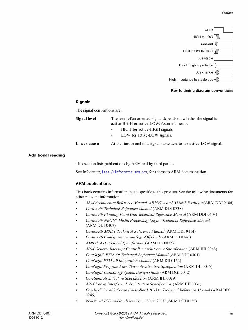
The figure named Key to timing diagram conventions on page viii explains the components used in timing diagrams. Variations, when they occur, have clear labels. You must not assume any timing information that is not explicit in the diagrams.
Shaded bus and signal areas are undefined, so the bus or signal can assume any value within the shaded area at that time. The actual level is unimportant and does not affect normal operation.
ARM DDI 0407I Copyright © 2008-2012 ARM. All rights reserved. viiID091612 Non-Confidential
Preface
Key to timing diagram conventions
Signals
The signal conventions are:
Signal level The level of an asserted signal depends on whether the signal is active-HIGH or active-LOW. Asserted means:• HIGH for active-HIGH signals• LOW for active-LOW signals.
Lower-case n At the start or end of a signal name denotes an active-LOW signal.
Additional reading
This section lists publications by ARM and by third parties.
See Infocenter, http://infocenter.arm.com, for access to ARM documentation.
ARM publications
This book contains information that is specific to this product. See the following documents for other relevant information:• ARM Architecture Reference Manual, ARMv7-A and ARMv7-R edition (ARM DDI 0406)• Cortex-A9 Technical Reference Manual (ARM DDI 0338)• Cortex-A9 Floating-Point Unit Technical Reference Manual (ARM DDI 0408)• Cortex-A9 NEON™ Media Processing Engine Technical Reference Manual
(ARM DDI 0409)• Cortex-A9 MBIST Technical Reference Manual (ARM DDI 0414)• Cortex-A9 Configuration and Sign-Off Guide (ARM DII 0146)• AMBA® AXI Protocol Specification (ARM IHI 0022)• ARM Generic Interrupt Controller Architecture Specification (ARM IHI 0048)• CoreSight™ PTM-A9 Technical Reference Manual (ARM DDI 0401)• CoreSight PTM-A9 Integration Manual (ARM DII 0162)• CoreSight Program Flow Trace Architecture Specification (ARM IHI 0035)• CoreSight Technology System Design Guide (ARM DGI 0012)• CoreSight Architecture Specification (ARM IHI 0029)• ARM Debug Interface v5 Architecture Specification (ARM IHI 0031)• Corelink™ Level 2 Cache Controller L2C-310 Technical Reference Manual (ARM DDI
0246)• RealView® ICE and RealView Trace User Guide (ARM DUI 0155).
Clock
HIGH to LOW
Transient
HIGH/LOW to HIGH
Bus stable
Bus to high impedance
Bus change
High impedance to stable bus
ARM DDI 0407I Copyright © 2008-2012 ARM. All rights reserved. viiiID091612 Non-Confidential

Preface
Other publications
This section lists relevant documents published by third parties:
• JEP106M, Standard Manufacture’s Identification Code, JEDEC Solid State Technology Association.
ARM DDI 0407I Copyright © 2008-2012 ARM. All rights reserved. ixID091612 Non-Confidential
Preface
FeedbackARM welcomes feedback on this product and its documentation.
Feedback on this product
If you have any comments or suggestions about this product, contact your supplier and give:
• The product name.
• The product revision or version.
• An explanation with as much information as you can provide. Include symptoms and diagnostic procedures if appropriate.
Feedback on content
If you have comments on content then send an e-mail to [email protected]. Give:• the title• the number, ARM DDI 0407I• the page numbers to which your comments apply• a concise explanation of your comments.
ARM also welcomes general suggestions for additions and improvements.
Note ARM tests the PDF only in Adobe Acrobat and Acrobat Reader, and cannot guarantee the quality of the represented document when used with any other PDF reader.
ARM DDI 0407I Copyright © 2008-2012 ARM. All rights reserved. xID091612 Non-Confidential
Chapter 1 Introduction
This chapter introduces the Cortex-A9 MPCore processor and its features. It contains the following sections:• About the Cortex-A9 MPCore processor on page 1-2• Compliance on page 1-4• Configurable options on page 1-5• Test features on page 1-6• Private Memory Region on page 1-7• Interfaces on page 1-9• MPCore considerations on page 1-10• Product documentation and design flow on page 1-11.• Product revisions on page 1-13.
ARM DDI 0407I Copyright © 2008-2012 ARM. All rights reserved. 1-1ID091612 Non-Confidential
Introduction
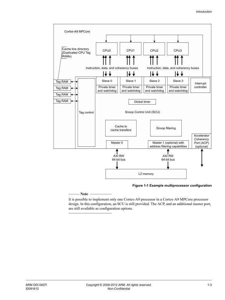
1.1 About the Cortex-A9 MPCore processorThe Cortex-A9 MPCore processor consists of:• From one to four Cortex-A9 processors in a cluster and a Snoop Control Unit (SCU) that
can be used to ensure coherency within the cluster.• A set of private memory-mapped peripherals, including a global timer, and a watchdog
and private timer for each Cortex-A9 processor present in the cluster.• An integrated Interrupt Controller that is an implementation of the Generic Interrupt
Controller architecture. The integrated Interrupt Controller registers are in the private memory region of the Cortex-A9 MPCore processor.
Individual Cortex-A9 processors in the Cortex-A9 MPCore cluster can be implemented with their own hardware configurations. See the Cortex-A9 Technical Reference Manual for additional information on possible Cortex-A9 processor configurations. ARM recommends you implement uniform configurations for software ease of use.
There are other configuration options that impact Cortex-A9 MPCore system integration. The major options are:
• One or two AXI master port interfaces, with address filtering capabilities
• An optional Accelerator Coherency Port (ACP) suitable for coherent memory transfers
• A configurable number of interrupt lines.
See Configurable options on page 1-5.
Figure 1-1 on page 1-3 shows an example multiprocessor configuration.
ARM DDI 0407I Copyright © 2008-2012 ARM. All rights reserved. 1-2ID091612 Non-Confidential
Introduction
Figure 1-1 Example multiprocessor configuration
Note It is possible to implement only one Cortex-A9 processor in a Cortex-A9 MPCore processor design. In this configuration, an SCU is still provided. The ACP, and an additional master port, are still available as configuration options.
CPU0
AXI RW64-bit bus
AXI RW64-bit bus
Slave 0
Private timer and watchdog
CPU1
Slave 1
Private timer and watchdog
CPU2
Slave 2
Private timer and watchdog
CPU3
Slave 3
Private timer and watchdog
Interrupt controller
Accelerator Coherency Port (ACP)(optional)
Master 0 Master 1 (optional) with address filtering capabilities
Tag control
Tag RAM
Tag RAM
Tag RAM
Tag RAM
Snoop Control Unit (SCU)
Instruction, data, and coherency buses Instruction, data, and coherency buses
Cache tocache transfers Snoop filtering
Cache line directory(Duplicated CPU Tag RAMs)
Global timer
L2 memory
Cortex-A9 MPCore
ARM DDI 0407I Copyright © 2008-2012 ARM. All rights reserved. 1-3ID091612 Non-Confidential
Introduction
1.2 ComplianceThe Cortex-A9 processor complies with, or implements, the specifications described in:• ARM architecture• Advanced Microcontroller Bus Architecture• Program Flow Trace architecture• Debug architecture• Generic Interrupt Controller architecture
This TRM complements architecture reference manuals, architecture specifications, protocol specifications, and relevant external standards. It does not duplicate information from these sources.
1.2.1 ARM architecture
The Cortex-A9 processor implements the ARMv7-A architecture profile that includes the following architecture extensions:
• Advanced Single Instruction Multiple Data (SIMD) architecture extension for integer and floating-point vector operations
• Vector Floating-Point version 3 (VFPv3) architecture extension for floating-point computation that is fully compliant with the IEEE 754 standard
• Security Extensions for enhanced security
• Multiprocessing Extensions for multiprocessing functionality.
See the ARM Architecture Reference Manual, ARMv7-A and ARMv7-R edition.
1.2.2 Advanced Microcontroller Bus Architecture
The Cortex-A9 processor complies with the AMBA 3 protocol. See the AMBA AXI Protocol Specification.
1.2.3 Program Flow Trace architecture
The Cortex-A9 processor implements the Program Trace Macrocell (PTM) based on the Program Flow Trace (PFT) v1.0 architecture profile. See the CoreSight Program Flow Trace Architecture Specification.
1.2.4 Debug architecture
The Cortex-A9 processor implements the ARMv7 Debug architecture profile, that includes support for Security Extensions and CoreSight. See the CoreSight Architecture Specification.
1.2.5 Generic Interrupt Controller architecture
The Cortex-A9 processor implements the ARM Generic Interrupt Controller (GIC) v1.0 architecture profile.
ARM DDI 0407I Copyright © 2008-2012 ARM. All rights reserved. 1-4ID091612 Non-Confidential
Introduction
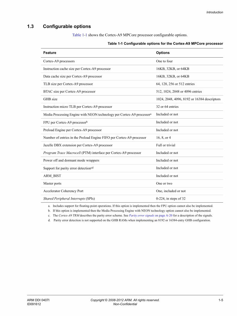
1.3 Configurable optionsTable 1-1 shows the Cortex-A9 MPCore processor configurable options.
Table 1-1 Configurable options for the Cortex-A9 MPCore processor
Feature Options
Cortex-A9 processors One to four
Instruction cache size per Cortex-A9 processor 16KB, 32KB, or 64KB
Data cache size per Cortex-A9 processor 16KB, 32KB, or 64KB
TLB size per Cortex-A9 processor 64, 128, 256 or 512 entries
BTAC size per Cortex-A9 processor 512, 1024, 2048 or 4096 entries
GHB size 1024, 2048, 4096, 8192 or 16384 descriptors
Instruction micro TLB per Cortex-A9 processor 32 or 64 entries
Media Processing Engine with NEON technology per Cortex-A9 processora Included or not
FPU per Cortex-A9 processorb Included or not
Preload Engine per Cortex-A9 processor Included or not
Number of entries in the Preload Engine FIFO per Cortex-A9 processor 16, 8, or 4
Jazelle DBX extension per Cortex-A9 processor Full or trivial
Program Trace Macrocell (PTM) interface per Cortex-A9 processor Included or not
Power off and dormant mode wrappers Included or not
Support for parity error detectioncd Included or not
ARM_BIST Included or not
Master ports One or two
Accelerator Coherency Port One, included or not
Shared Peripheral Interrupts (SPIs) 0-224, in steps of 32
a. Includes support for floating-point operations. If this option is implemented then the FPU option cannot also be implemented.b. If this option is implemented then the Media Processing Engine with NEON technology option cannot also be implemented.c. The Cortex-A9 TRM describes the parity error scheme. See Parity error signals on page A-20 for a description of the signals.d. Parity error detection is not supported on the GHB RAMs when implementing an 8192 or 16384-entry GHB configuration.
ARM DDI 0407I Copyright © 2008-2012 ARM. All rights reserved. 1-5ID091612 Non-Confidential
Introduction
1.4 Test featuresThe Cortex-A9 processor provides test signals that enable the use of both ATPG and MBIST to test the Cortex-A9 processor and its memory arrays. See Appendix A Signal Descriptions and Cortex-A9 MBIST Controller Technical Reference Manual.
ARM DDI 0407I Copyright © 2008-2012 ARM. All rights reserved. 1-6ID091612 Non-Confidential
Introduction
1.5 Private Memory RegionAll registers accessible by all Cortex-A9 processors within the Cortex-A9 MPCore are grouped into two contiguous 4KB pages accessed through a dedicated internal bus. The base address of these pages is defined by the pins PERIPHBASE[31:13]. See Configuration signals on page A-5 for more information on PERIPHBASE[31:13].
Cortex-A9 MPCore global control and peripherals must be accessed through memory-mapped transfers to the Cortex-A9 MPCore private memory region.
Memory regions used for these registers must be marked as Device or Strongly-ordered in the translation tables.
Access to the private memory region is little-endian only.
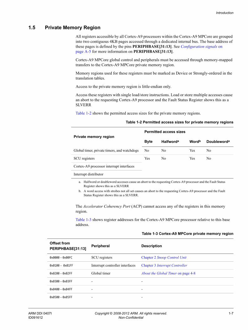
Access these registers with single load/store instructions. Load or store multiple accesses cause an abort to the requesting Cortex-A9 processor and the Fault Status Register shows this as a SLVERR
Table 1-2 shows the permitted access sizes for the private memory regions.
The Accelerator Coherency Port (ACP) cannot access any of the registers in this memory region.
Table 1-3 shows register addresses for the Cortex-A9 MPCore processor relative to this base address.
Table 1-2 Permitted access sizes for private memory regions
Private memory regionPermitted access sizes
Byte Halfworda
a. Halfword or doubleword accesses cause an abort to the requesting Cortex-A9 processor and the Fault Status Register shows this as a SLVERR
Wordb
b. A word access with strobes not all set causes an abort to the requesting Cortex-A9 processor and the Fault Status Register shows this as a SLVERR.
Doubleworda
Global timer, private timers, and watchdogs No No Yes No
SCU registers Yes No Yes No
Cortex-A9 processor interrupt interfaces
Interrupt distributor
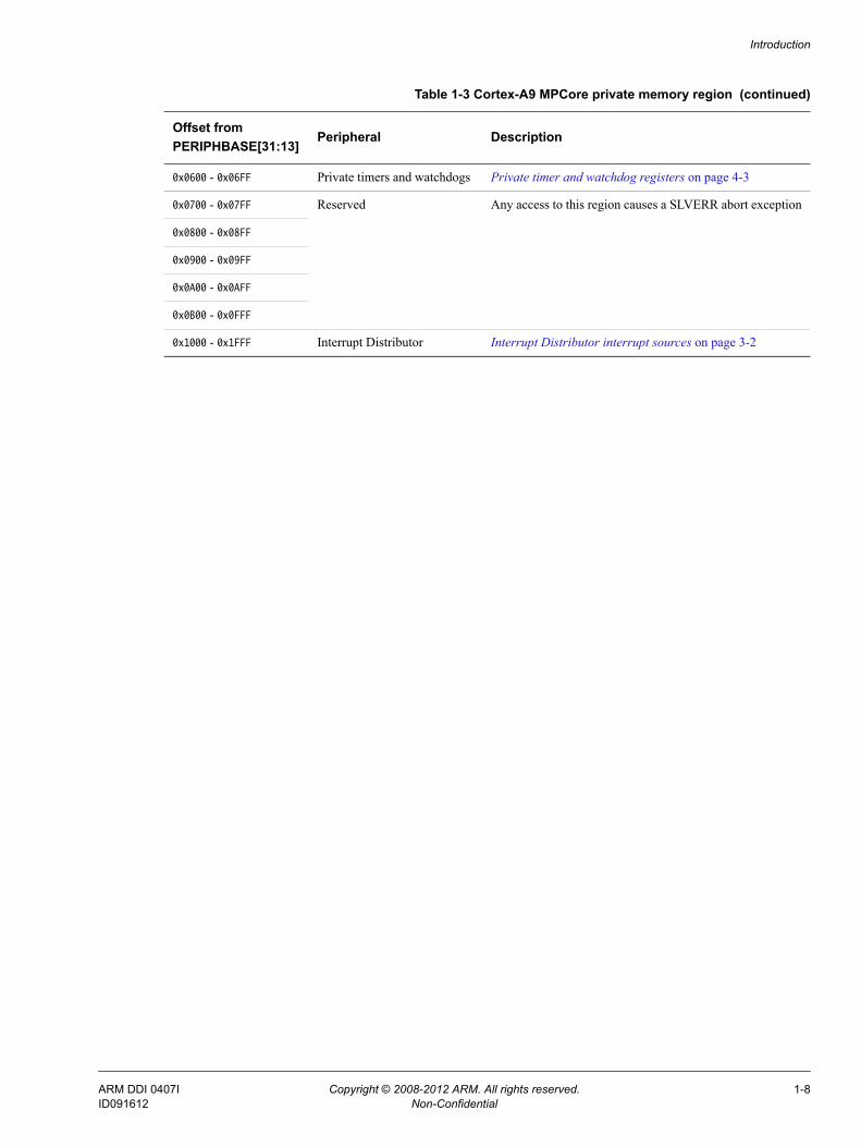
Table 1-3 Cortex-A9 MPCore private memory region
Offset fromPERIPHBASE[31:13]
Peripheral Description
0x0000 - 0x00FC SCU registers Chapter 2 Snoop Control Unit
0x0100 - 0x01FF Interrupt controller interfaces Chapter 3 Interrupt Controller
0x0200 - 0x02FF Global timer About the Global Timer on page 4-8
0x0300 - 0x03FF - -
0x0400 - 0x04FF - -
0x0500 - 0x05FF - -
ARM DDI 0407I Copyright © 2008-2012 ARM. All rights reserved. 1-7ID091612 Non-Confidential
Introduction
0x0600 - 0x06FF Private timers and watchdogs Private timer and watchdog registers on page 4-3
0x0700 - 0x07FF Reserved Any access to this region causes a SLVERR abort exception
0x0800 - 0x08FF
0x0900 - 0x09FF
0x0A00 - 0x0AFF
0x0B00 - 0x0FFF
0x1000 - 0x1FFF Interrupt Distributor Interrupt Distributor interrupt sources on page 3-2
Table 1-3 Cortex-A9 MPCore private memory region (continued)
Offset fromPERIPHBASE[31:13]
Peripheral Description
ARM DDI 0407I Copyright © 2008-2012 ARM. All rights reserved. 1-8ID091612 Non-Confidential
Introduction
1.6 InterfacesThe Cortex-A9 MPCore processor has the following interfaces:• AMBA AXI interfaces• Interrupts interface.• Debug interfaces• Design for Test interface
1.6.1 AMBA AXI interfaces
The AMBA AXI interfaces include one or two AXI Master port interfaces, and one Accelerator Coherency (ACP) AXI Slave port. See AMBA AXI Master Port Interfaces on page 2-13. See also the AMBA AXI Protocol Specification.
1.6.2 Interrupts interface
The Cortex-A9 MPCore processor provides the legacy nIRQ and nFIQ interrupt lines for each individual Cortex-A9 processor present in the cluster.
The Cortex-A9 MPCore processor also provides a separate interrupt interface, with a configurable number of interrupts lines, up to 224, connected to its internal Interrupt Controller.
See Chapter 3 Interrupt Controller.
1.6.3 Debug interfaces
The external debug interface of the Cortex-A9 MPCore processor is compliant with the ARMv7 Debug Architecture that includes support for Security Extensions and CoreSight.
With the exception of a few debug configuration signals, the debug interfaces of the individual Cortex-A9 processors are presented externally so that each processor can be debugged independently.
The Cortex-A9 MPCore processor also provides an external Debug APB interface for memory-mapped accesses to debug and performance monitor registers.
See Chapter 6 Debug.
1.6.4 Design for Test interface
The Cortex-A9 MBIST Controller Technical Reference Manual gives information on the MBIST interface.
ARM DDI 0407I Copyright © 2008-2012 ARM. All rights reserved. 1-9ID091612 Non-Confidential
Introduction
1.7 MPCore considerationsThis section describes multiprocessing considerations. It contains the following sections:• About Cortex-A9 MPCore coherency• Registers with multiprocessor uses• Maintenance operations broadcasting.
1.7.1 About Cortex-A9 MPCore coherency
Memory coherency in a Cortex-A9 MPCore processor is maintained following a weakly ordered memory consistency model.
Cache coherency among L1 data caches of the Cortex-A9 processors in the cluster is maintained when the Cortex-A9 processors are operating in Symmetric Multi-Processing (SMP) mode. This mode is controlled by the SMP bit of the Auxiliary Control Register.
To be kept coherent, the memory must be marked as Write-Back, Shareable, Normal memory.
Note When the Shareable attribute is applied to a memory region that is not Write-Back Normal memory, data held in this region is treated as Noncacheable.
1.7.2 Registers with multiprocessor uses
The following registers, described in the Cortex-A9 TRM, have multiprocessor uses.• Auxiliary Control Register• Configuration Base Address Register• Multiprocessor Affinity Register.
1.7.3 Maintenance operations broadcasting
All processors working in SMP mode on the same coherent domain can send and receive TLB and Cache Maintenance operations. The ARM Architecture Reference Manual gives detailed information on broadcast operations.A Cortex-A9 processor in the A9-MP cluster broadcasts broadcastable maintenance operation when it operates in SMP mode (ACTLR.SMP=1) and when the maintenance operation broadcasting is enabled (ACTLR.FW=1).A Cortex-A9 processor can receive and execute broadcast maintenance operations when it operates in SMP mode, ACTLR.SMP=1.
ARM DDI 0407I Copyright © 2008-2012 ARM. All rights reserved. 1-10ID091612 Non-Confidential
Introduction
1.8 Product documentation and design flowThis section describes the Cortex-A9 MPCore books and how they relate to the design flow. It includes:• Documentation• Design flow.
See Additional reading on page viii for more information about the books described in this section. For information on the relevant architectural standards and protocols, see Compliance on page 1-4.
1.8.1 Documentation
The Cortex-A9 MPCore documentation is as follows:
Technical Reference Manual The Technical Reference Manual (TRM) describes the functionality and the effects of functional options on the behavior of the Cortex-A9 MPCore processor. It is required at all stages of the design flow. The choices made in the design flow can mean that some behavior described in the TRM is not relevant. If you are programming the Cortex-A9 MPCore processor then contact:• the implementer to determine:
— the build configuration of the implementation— what integration, if any, was performed before implementing the
Cortex-A9 MPCore processor• the integrator to determine the pin configuration of the device that you are
using.
1.8.2 Design flow
The Cortex-A9 MPCore processor is delivered as synthesizable RT. Before it can be used in a product, it must go through the following processes:
Implementation The implementer configures and synthesizes the RTL to produce a hard macrocell. This might include integrating RAMs into the design.
Integration The integrator connects the implemented design into a SoC. This includes connecting it to a memory system and peripherals.
Programming This is the last process. The system programmer develops the software required to configure and initialize the Cortex-A9 MPCore processor, and tests the required application software.
Each process:
• can be performed by a different party
• can include implementation and integration choices affect the behavior and features of the Cortex-A9 MPCore processor.
For MCUs, often a single design team integrates the processor before synthesizing the complete design. Alternatively, the team can synthesise the processor on its own or partially integrated, to produce a macrocell that is then integrated, possibly by a separate team.
ARM DDI 0407I Copyright © 2008-2012 ARM. All rights reserved. 1-11ID091612 Non-Confidential
Introduction
The operation of the final device depends on:
Build configuration The implementer chooses the options that affect how the RTL source files are pre-processed. These options usually include or exclude logic that affects one or more of the area, maximum frequency, and features of the resulting macrocell.
Configuration inputs The integrator configures some features of the Cortex-A9 MPCore processor by tying inputs to specific values. These configurations affect the start-up behavior before any software configuration is made. They can also limit the options available to the software.
Software configuration The programmer configures the Cortex-A9 MPCore processor by programming particular values into registers. This affects the behavior of the Cortex-A9 MPCore processor.
Note This manual refers to implementation-defined features that are applicable to build configuration options. Reference to a feature that is included means that the appropriate build and pin configuration options are selected. Reference to an enabled feature means one that has also been configured by software.
ARM DDI 0407I Copyright © 2008-2012 ARM. All rights reserved. 1-12ID091612 Non-Confidential
Introduction
1.9 Product revisionsThis section describes the differences in functionality between product revisions. These differences are in addition to the those described in the Cortex-A9 TRM:
r0p0 First release.
r0p0-r0p1 The differences between the two revisions are:• r0p1 includes fixes for all known engineering errata relating to r0p0• r0p1 includes an upgrade of the micro TLB entries from 8 to 32 entries, on
both the Instruction and Data side.Neither of these changes affect the functionality described in this document.
r0p1-r1p0 Functional changes are:• In r1p0 there is a global timer. See About the Global Timer on page 4-8.• In the Interrupt Controller INT becomes IRQS. See SPI Status Registers on
page 3-11.• SCU CPU Power Status Register bits reassigned. See SCU CPU Power
Status Register on page 2-6.
r1p0-r2p0 Functional changes are:• Conditions for coherent snoop for ACP requests amended. See ACP
requests on page 2-20.• SCU Control register updated. See SCU Control Register on page 2-3:
— Bit 6 to enable additional clock gating on GIC, — Bit 5 to enable additional clock gating on SCU.
• SCU Secure Access Control Register renamed to SCU Non-secure Access Control Register. See SCU Non-secure Access Control Register on page 2-11.
• Removal of SCU Invalidate All Registers in Non-secure State Register and functionality. See Table 2-1 on page 2-3.
• Added speculative linefill feature to optimize L1 miss and L2 hit latency, See SCU Control Register on page 2-3. Bit 3.
• Added SCUIDLE output. See SCU CPU Power Status Register on page 2-6
• Added Filtering capabilities in the SCU for Device accesses. See Device accesses filtering on page 2-17.
• PERIPHCLK can be turned off. See Clocks on page 5-2• Change to the behavior of the comparators for each processor with the
global timer. See About the Global Timer on page 4-8• Added PMUEVENT See Performance monitoring signals on page A-18
r2p0-r2p1 No change.
r2p1-r2p2 No change.
r2p2-r3p0 No change.
r3p0-r4p0 Added configuration options for the TLB, BTAC and GHB sizes. See Configurable options on page 1-5.
r4p0-r4p1 No change.
ARM DDI 0407I Copyright © 2008-2012 ARM. All rights reserved. 1-13ID091612 Non-Confidential
Chapter 2 Snoop Control Unit
This chapter describes the Snoop Control Unit (SCU). It contains the following sections:• About the SCU on page 2-2• SCU registers on page 2-3.• AMBA AXI Master Port Interfaces on page 2-13• Accelerator Coherency Port on page 2-20• Event communication with an external agent using WFE/SEV on page 2-23.
ARM DDI 0407I Copyright © 2008-2012 ARM. All rights reserved. 2-1ID091612 Non-Confidential
Snoop Control Unit
2.1 About the SCUThe SCU connects one to four Cortex-A9 processors to the memory system through the AXI interfaces.
The SCU functions are to:• maintain data cache coherency between the Cortex-A9 processors• initiate L2 AXI memory accesses• arbitrate between Cortex-A9 processors requesting L2 accesses• manage ACP accesses.
Note The Cortex-A9 SCU does not support hardware management of coherency of the instruction cache.
2.1.1 TrustZone extensions
The SCU implements support for the ARM Architecture security extensions. See SCU Access Control Register (SAC) on page 2-10 See SCU Non-secure Access Control Register on page 2-11.
2.1.2 SCU event monitoring
The individual CPU event monitors can be configured to gather statistics on the operation of the SCU. The Cortex-A9 TRM describes event monitoring.
ARM DDI 0407I Copyright © 2008-2012 ARM. All rights reserved. 2-2ID091612 Non-Confidential
Snoop Control Unit
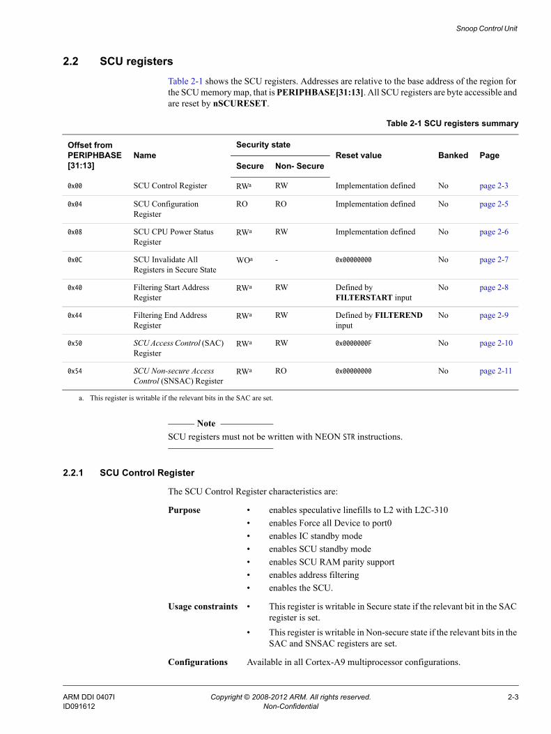
2.2 SCU registersTable 2-1 shows the SCU registers. Addresses are relative to the base address of the region for the SCU memory map, that is PERIPHBASE[31:13]. All SCU registers are byte accessible and are reset by nSCURESET.
Note SCU registers must not be written with NEON STR instructions.
2.2.1 SCU Control Register
The SCU Control Register characteristics are:
Purpose • enables speculative linefills to L2 with L2C-310• enables Force all Device to port0• enables IC standby mode• enables SCU standby mode• enables SCU RAM parity support• enables address filtering• enables the SCU.
Usage constraints • This register is writable in Secure state if the relevant bit in the SAC register is set.
• This register is writable in Non-secure state if the relevant bits in the SAC and SNSAC registers are set.
Configurations Available in all Cortex-A9 multiprocessor configurations.
Table 2-1 SCU registers summary
Offset from PERIPHBASE [31:13]
NameSecurity state
Reset value Banked PageSecure Non- Secure
0x00 SCU Control Register RWa RW Implementation defined No page 2-3
0x04 SCU Configuration Register
RO RO Implementation defined No page 2-5
0x08 SCU CPU Power Status Register
RWa RW Implementation defined No page 2-6
0x0C SCU Invalidate All Registers in Secure State
WOa - 0x00000000 No page 2-7
0x40 Filtering Start Address Register
RWa RW Defined by FILTERSTART input
No page 2-8
0x44 Filtering End Address Register
RWa RW Defined by FILTEREND input
No page 2-9
0x50 SCU Access Control (SAC) Register
RWa RW 0x0000000F No page 2-10
0x54 SCU Non-secure Access Control (SNSAC) Register
RWa RO 0x00000000 No page 2-11
a. This register is writable if the relevant bits in the SAC are set.
ARM DDI 0407I Copyright © 2008-2012 ARM. All rights reserved. 2-3ID091612 Non-Confidential
Snoop Control Unit
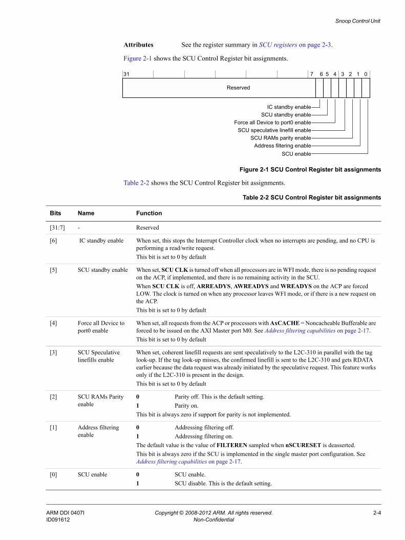
Attributes See the register summary in SCU registers on page 2-3.
Figure 2-1 shows the SCU Control Register bit assignments.
Figure 2-1 SCU Control Register bit assignments
Table 2-2 shows the SCU Control Register bit assignments.
31 1 0
Reserved
SCU enableAddress filtering enable
23
SCU RAMs parity enable
SCU standby enableForce all Device to port0 enable
SCU speculative linefill enable
IC standby enable
4567
Table 2-2 SCU Control Register bit assignments
Bits Name Function
[31:7] - Reserved
[6] IC standby enable When set, this stops the Interrupt Controller clock when no interrupts are pending, and no CPU is performing a read/write request.This bit is set to 0 by default
[5] SCU standby enable When set, SCU CLK is turned off when all processors are in WFI mode, there is no pending request on the ACP, if implemented, and there is no remaining activity in the SCU. When SCU CLK is off, ARREADYS, AWREADYS and WREADYS on the ACP are forced LOW. The clock is turned on when any processor leaves WFI mode, or if there is a new request on the ACP.This bit is set to 0 by default
[4] Force all Device to port0 enable
When set, all requests from the ACP or processors with AxCACHE = Noncacheable Bufferable are forced to be issued on the AXI Master port M0. See Address filtering capabilities on page 2-17.This bit is set to 0 by default
[3] SCU Speculative linefills enable
When set, coherent linefill requests are sent speculatively to the L2C-310 in parallel with the tag look-up. If the tag look-up misses, the confirmed linefill is sent to the L2C-310 and gets RDATA earlier because the data request was already initiated by the speculative request. This feature works only if the L2C-310 is present in the design.This bit is set to 0 by default
[2] SCU RAMs Parity enable
0 Parity off. This is the default setting. 1 Parity on.This bit is always zero if support for parity is not implemented.
[1] Address filtering enable
0 Addressing filtering off. 1 Addressing filtering on.The default value is the value of FILTEREN sampled when nSCURESET is deasserted.This bit is always zero if the SCU is implemented in the single master port configuration. See Address filtering capabilities on page 2-17.
[0] SCU enable 0 SCU enable. 1 SCU disable. This is the default setting.
ARM DDI 0407I Copyright © 2008-2012 ARM. All rights reserved. 2-4ID091612 Non-Confidential
Snoop Control Unit
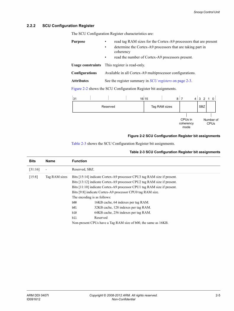
2.2.2 SCU Configuration Register
The SCU Configuration Register characteristics are:
Purpose • read tag RAM sizes for the Cortex-A9 processors that are present• determine the Cortex-A9 processors that are taking part in
coherency• read the number of Cortex-A9 processors present.
Usage constraints This register is read-only.
Configurations Available in all Cortex-A9 multiprocessor configurations.
Attributes See the register summary in SCU registers on page 2-3.
Figure 2-2 shows the SCU Configuration Register bit assignments.
Figure 2-2 SCU Configuration Register bit assignments
Table 2-3 shows the SCU Configuration Register bit assignments.
31 16 15 8 7 4 2 1 0
Tag RAM sizes
CPUs in coherency
mode
SBZReserved
Number of CPUs
3
Table 2-3 SCU Configuration Register bit assignments
Bits Name Function
[31:16] - Reserved, SBZ.
[15:8] Tag RAM sizes Bits [15:14] indicate Cortex-A9 processor CPU3 tag RAM size if present.Bits [13:12] indicate Cortex-A9 processor CPU2 tag RAM size if present.Bits [11:10] indicate Cortex-A9 processor CPU1 tag RAM size if present.Bits [9:8] indicate Cortex-A9 processor CPU0 tag RAM size.The encoding is as follows:b00 16KB cache, 64 indexes per tag RAM.b01 32KB cache, 128 indexes per tag RAM.b10 64KB cache, 256 indexes per tag RAM.b11 Reserved Non-present CPUs have a Tag RAM size of b00, the same as 16KB.
ARM DDI 0407I Copyright © 2008-2012 ARM. All rights reserved. 2-5ID091612 Non-Confidential
Snoop Control Unit
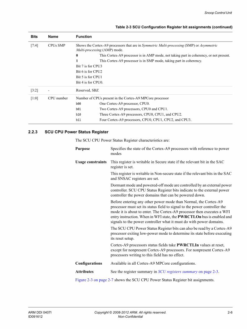
2.2.3 SCU CPU Power Status Register
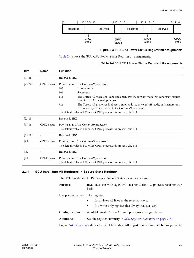
The SCU CPU Power Status Register characteristics are:
Purpose Specifies the state of the Cortex-A9 processors with reference to power modes
Usage constraints This register is writable in Secure state if the relevant bit in the SAC register is set.This register is writable in Non-secure state if the relevant bits in the SAC and SNSAC registers are set.Dormant mode and powered-off mode are controlled by an external power controller. SCU CPU Status Register bits indicate to the external power controller the power domains that can be powered down.Before entering any other power mode than Normal, the Cortex-A9 processor must set its status field to signal to the power controller the mode it is about to enter. The Cortex-A9 processor then executes a WFI entry instruction. When in WFI state, the PWRCTLOn bus is enabled and signals to the power controller what it must do with power domains.The SCU CPU Power Status Register bits can also be read by a Cortex-A9 processor exiting low-power mode to determine its state before executing its reset setup.Cortex-A9 processors status fields take PWRCTLIn values at reset, except for nonpresent Cortex-A9 processors. For nonpresent Cortex-A9 processors writing to this field has no effect.
Configurations Available in all Cortex-A9 MPCore configurations.
Attributes See the register summary in SCU registers summary on page 2-3.
Figure 2-3 on page 2-7 shows the SCU CPU Power Status Register bit assignments.
[7:4] CPUs SMP Shows the Cortex-A9 processors that are in Symmetric Multi-processing (SMP) or Asymmetric Multi-processing (AMP) mode.0 This Cortex-A9 processor is in AMP mode, not taking part in coherency, or not present.1 This Cortex-A9 processor is in SMP mode, taking part in coherency.Bit 7 is for CPU3Bit 6 is for CPU2Bit 5 is for CPU1Bit 4 is for CPU0.
[3:2] - Reserved, SBZ
[1:0] CPU number Number of CPUs present in the Cortex-A9 MPCore processorb00 One Cortex-A9 processor, CPU0.b01 Two Cortex-A9 processors, CPU0 and CPU1.b10 Three Cortex-A9 processors, CPU0, CPU1, and CPU2.b11 Four Cortex-A9 processors, CPU0, CPU1, CPU2, and CPU3.
Table 2-3 SCU Configuration Register bit assignments (continued)
Bits Name Function
ARM DDI 0407I Copyright © 2008-2012 ARM. All rights reserved. 2-6ID091612 Non-Confidential
Snoop Control Unit
Figure 2-3 SCU CPU Power Status Register bit assignments
Table 2-4 shows the SCU CPU Power Status Register bit assignments.
2.2.4 SCU Invalidate All Registers in Secure State Register
The SCU Invalidate All Registers in Secure State characteristics are:
Purpose Invalidates the SCU tag RAMs on a per Cortex-A9 processor and per way basis.
Usage constraints This register:• Invalidates all lines in the selected ways.• Is a write-only register that always reads as zero.
Configurations Available in all Cortex-A9 multiprocessor configurations.
Attributes See the register summary in SCU registers summary on page 2-3.
Figure 2-4 on page 2-8 shows the SCU Invalidate All Register in Secure state bit assignments.
7 2 1 0
Reserved
CPU3 status
CPU2 status
CPU1 status
CPU0 status
31 8
Reserved Reserved Reserved
26 25 24 23 18 17 16 15 10 9
Table 2-4 SCU CPU Power Status Register bit assignments
Bits Name Function
[31:26] - Reserved, SBZ
[25:24] CPU3 status Power status of the Cortex-A9 processor:b00 Normal mode.b01 Reserved.b10 The Cortex-A9 processor is about to enter, or is in, dormant mode. No coherency request
is sent to the Cortex-A9 processor.b11 The Cortex-A9 processor is about to enter, or is in, powered-off mode, or is nonpresent.
No coherency request is sent to the Cortex-A9 processor.The default value is b00 when CPU3 processor is present, else b11
[23:18] - Reserved, SBZ
[17:16] CPU2 status Power status of the Cortex-A9 processor.The default value is b00 when CPU2 processor is present, else b11
[15:10] - Reserved, SBZ
[9:8] CPU1 status Power status of the Cortex-A9 processor.The default value is b00 when CPU1 processor is present, else b11
[7:2] - Reserved, SBZ
[1:0] CPU0 status Power status of the Cortex-A9 processor.The default value is b00 when CPU0 processor is present, else b11
ARM DDI 0407I Copyright © 2008-2012 ARM. All rights reserved. 2-7ID091612 Non-Confidential

Snoop Control Unit
Figure 2-4 SCU Invalidate All Registers in Secure state bit assignments
Table 2-5 shows the SCU Invalidate All Register in Secure state bit assignments.
2.2.5 Filtering Start Address Register
The Filtering Start Address Register characteristics are:
Purpose Provides the start address for use with master port 1 in a two-master port configuration.
Usage constraints This register is writable:• in Secure state if the relevant bit in the SAC register is set.• in Non-secure state if the relevant bits in the SAC and SNSAC
registers are set.
Configurations Available in all two-master port configurations. When only one master port is present these registers are not implemented. Writes have no effect and reads return a value 0x0 for all filtering registers.
Attributes See the register summary in SCU registers summary on page 2-3.
Figure 2-5 shows the Filtering Start Address Register bit assignments.
Figure 2-5 Filtering Start Address Register bit assignments
8 7 4 0
SBZ
3
CPU0 waysCPU1 ways
111215
CPU2 waysCPU3 ways
31 16
Table 2-5 SCU Invalidate All Registers in Secure state bit assignments
Bits Name Function
[31:16] - -
[15:12] CPU3 ways Specifies the ways that must be invalidated for CPU3. Writing to these bits has no effect if the Cortex-A9 MPCore processor has fewer than four processors.
[11:8] CPU2 ways Specifies the ways that must be invalidated for CPU2. Writing to these bits has no effect if the Cortex-A9 MPCore processor has fewer than three processors.
[7:4] CPU1 ways Specifies the ways that must be invalidated for CPU1. Writing to these bits has no effect if the Cortex-A9 MPCore processor has fewer than two processors.
[3:0] CPU0 ways Specifies the ways that must be invalidated for CPU0.
0
Filtering start address
31
SBZ
1920
ARM DDI 0407I Copyright © 2008-2012 ARM. All rights reserved. 2-8ID091612 Non-Confidential
Snoop Control Unit
Table 2-6 shows the Filtering Start Address Register bit assignments.
See Configuration signals on page A-5.
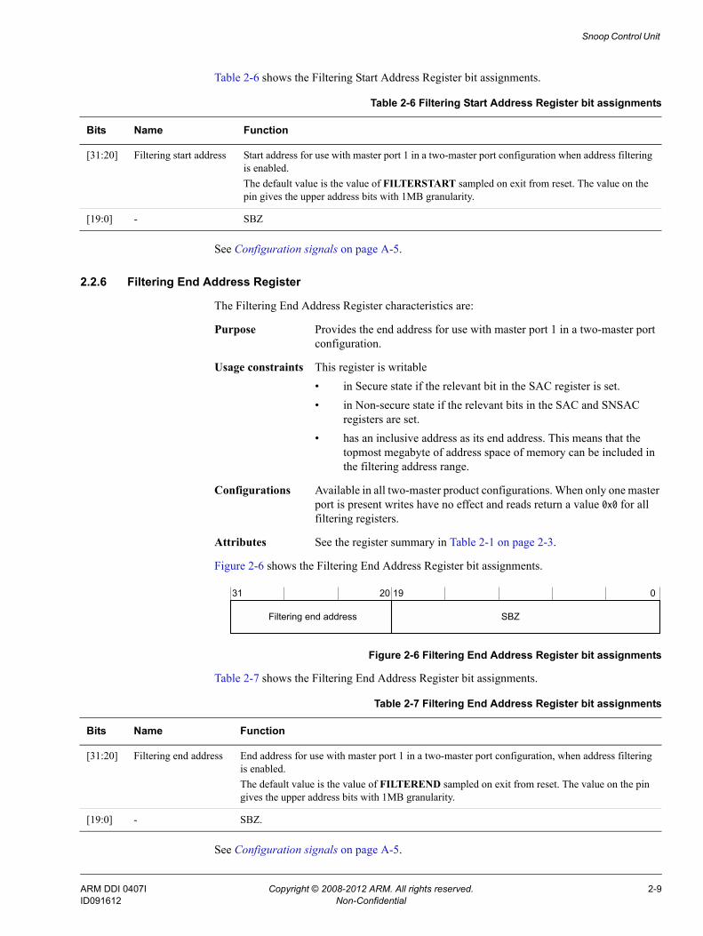
2.2.6 Filtering End Address Register
The Filtering End Address Register characteristics are:
Purpose Provides the end address for use with master port 1 in a two-master port configuration.
Usage constraints This register is writable• in Secure state if the relevant bit in the SAC register is set.• in Non-secure state if the relevant bits in the SAC and SNSAC
registers are set.• has an inclusive address as its end address. This means that the
topmost megabyte of address space of memory can be included in the filtering address range.
Configurations Available in all two-master product configurations. When only one master port is present writes have no effect and reads return a value 0x0 for all filtering registers.
Attributes See the register summary in Table 2-1 on page 2-3.
Figure 2-6 shows the Filtering End Address Register bit assignments.
Figure 2-6 Filtering End Address Register bit assignments
Table 2-7 shows the Filtering End Address Register bit assignments.
See Configuration signals on page A-5.
Table 2-6 Filtering Start Address Register bit assignments
Bits Name Function
[31:20] Filtering start address Start address for use with master port 1 in a two-master port configuration when address filtering is enabled.The default value is the value of FILTERSTART sampled on exit from reset. The value on the pin gives the upper address bits with 1MB granularity.
[19:0] - SBZ
0
Filtering end address
31
SBZ
1920
Table 2-7 Filtering End Address Register bit assignments
Bits Name Function
[31:20] Filtering end address End address for use with master port 1 in a two-master port configuration, when address filtering is enabled.The default value is the value of FILTEREND sampled on exit from reset. The value on the pin gives the upper address bits with 1MB granularity.
[19:0] - SBZ.
ARM DDI 0407I Copyright © 2008-2012 ARM. All rights reserved. 2-9ID091612 Non-Confidential
Snoop Control Unit
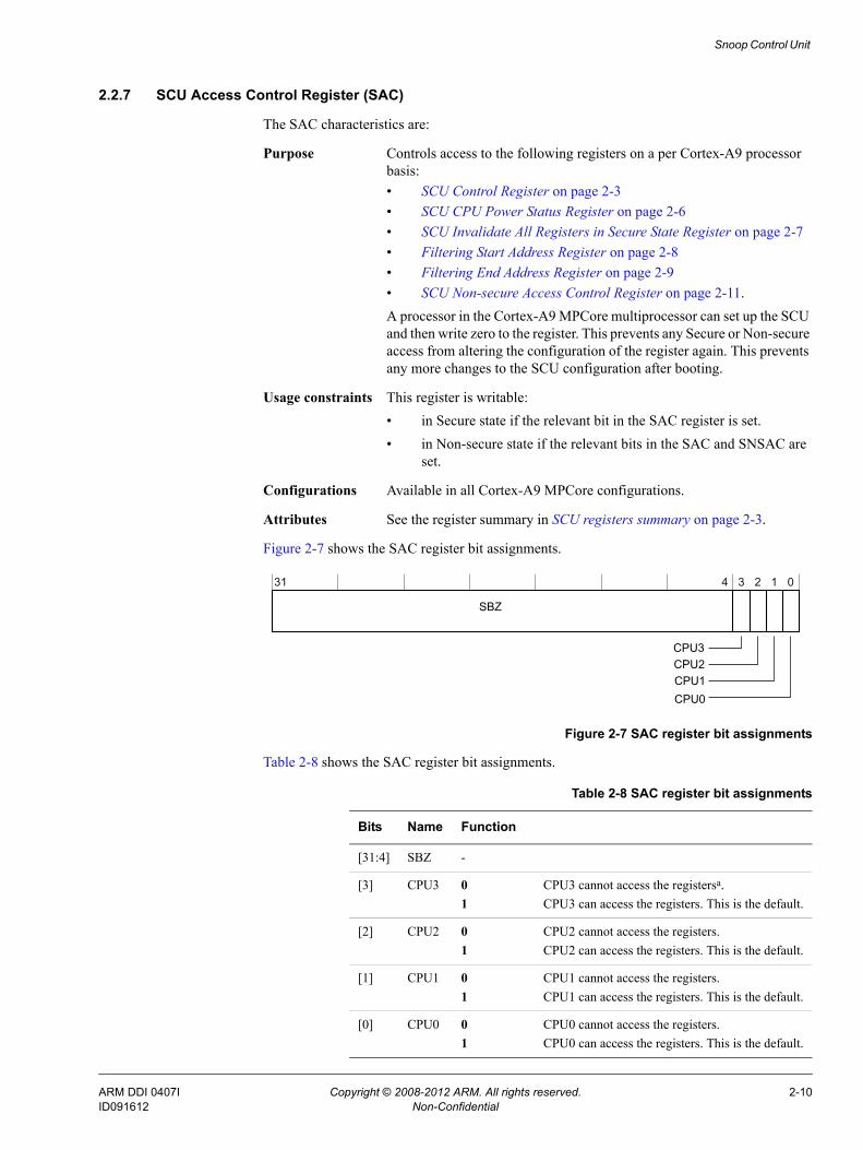
2.2.7 SCU Access Control Register (SAC)
The SAC characteristics are:
Purpose Controls access to the following registers on a per Cortex-A9 processor basis:• SCU Control Register on page 2-3• SCU CPU Power Status Register on page 2-6• SCU Invalidate All Registers in Secure State Register on page 2-7• Filtering Start Address Register on page 2-8• Filtering End Address Register on page 2-9• SCU Non-secure Access Control Register on page 2-11.A processor in the Cortex-A9 MPCore multiprocessor can set up the SCU and then write zero to the register. This prevents any Secure or Non-secure access from altering the configuration of the register again. This prevents any more changes to the SCU configuration after booting.
Usage constraints This register is writable:• in Secure state if the relevant bit in the SAC register is set.• in Non-secure state if the relevant bits in the SAC and SNSAC are
set.
Configurations Available in all Cortex-A9 MPCore configurations.
Attributes See the register summary in SCU registers summary on page 2-3.
Figure 2-7 shows the SAC register bit assignments.
Figure 2-7 SAC register bit assignments
Table 2-8 shows the SAC register bit assignments.
31 3 2 1 0
SBZ
CPU3CPU2CPU1CPU0
4
Table 2-8 SAC register bit assignments
Bits Name Function
[31:4] SBZ -
[3] CPU3 0 CPU3 cannot access the registersa.1 CPU3 can access the registers. This is the default.
[2] CPU2 0 CPU2 cannot access the registers.1 CPU2 can access the registers. This is the default.
[1] CPU1 0 CPU1 cannot access the registers.1 CPU1 can access the registers. This is the default.
[0] CPU0 0 CPU0 cannot access the registers.1 CPU0 can access the registers. This is the default.
ARM DDI 0407I Copyright © 2008-2012 ARM. All rights reserved. 2-10ID091612 Non-Confidential
Snoop Control Unit
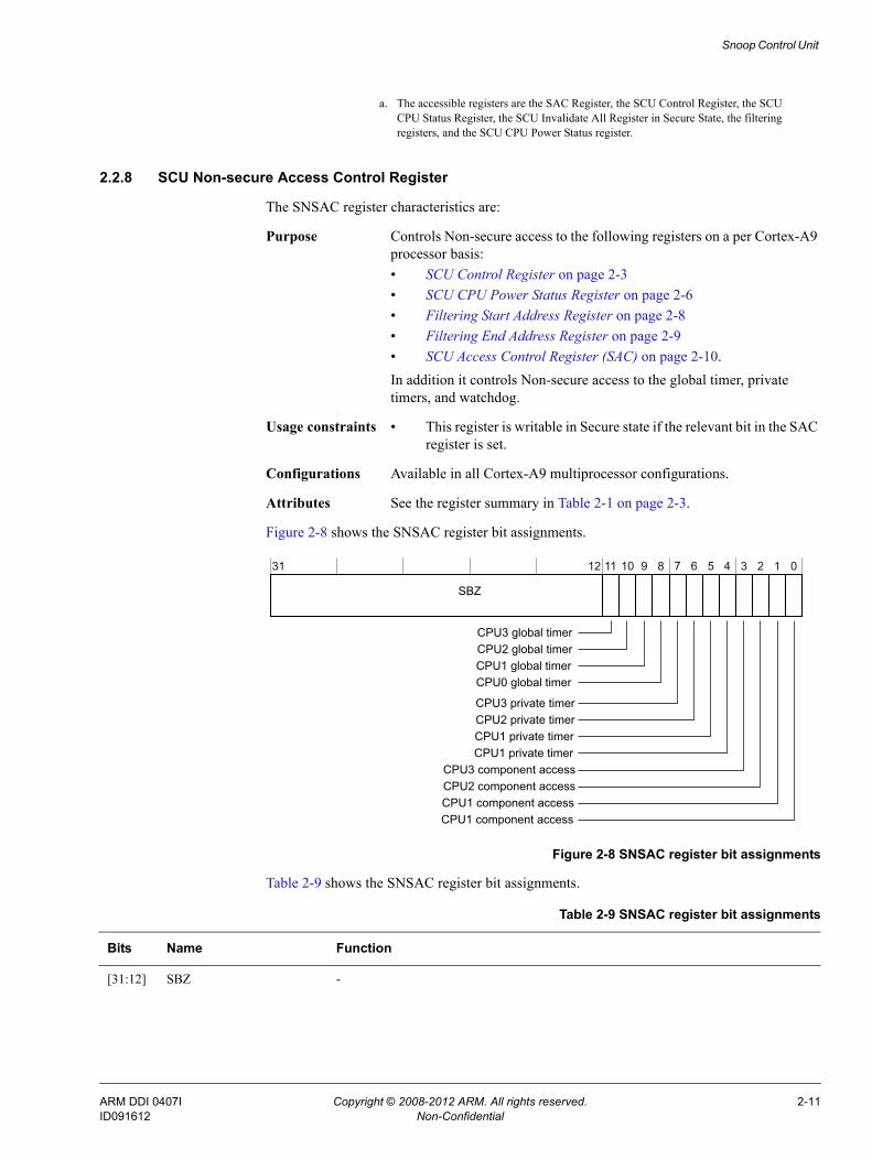
2.2.8 SCU Non-secure Access Control Register
The SNSAC register characteristics are:
Purpose Controls Non-secure access to the following registers on a per Cortex-A9 processor basis:• SCU Control Register on page 2-3• SCU CPU Power Status Register on page 2-6• Filtering Start Address Register on page 2-8• Filtering End Address Register on page 2-9• SCU Access Control Register (SAC) on page 2-10.In addition it controls Non-secure access to the global timer, private timers, and watchdog.
Usage constraints • This register is writable in Secure state if the relevant bit in the SAC register is set.
Configurations Available in all Cortex-A9 multiprocessor configurations.
Attributes See the register summary in Table 2-1 on page 2-3.
Figure 2-8 shows the SNSAC register bit assignments.
Figure 2-8 SNSAC register bit assignments
Table 2-9 shows the SNSAC register bit assignments.
a. The accessible registers are the SAC Register, the SCU Control Register, the SCU CPU Status Register, the SCU Invalidate All Register in Secure State, the filtering registers, and the SCU CPU Power Status register.
31 3 2 1 0
SBZ
48 7 6 59101112
CPU3 global timerCPU2 global timerCPU1 global timerCPU0 global timer
CPU3 private timerCPU2 private timerCPU1 private timerCPU1 private timer
CPU3 component accessCPU2 component accessCPU1 component accessCPU1 component access
Table 2-9 SNSAC register bit assignments
Bits Name Function
[31:12] SBZ -
ARM DDI 0407I Copyright © 2008-2012 ARM. All rights reserved. 2-11ID091612 Non-Confidential
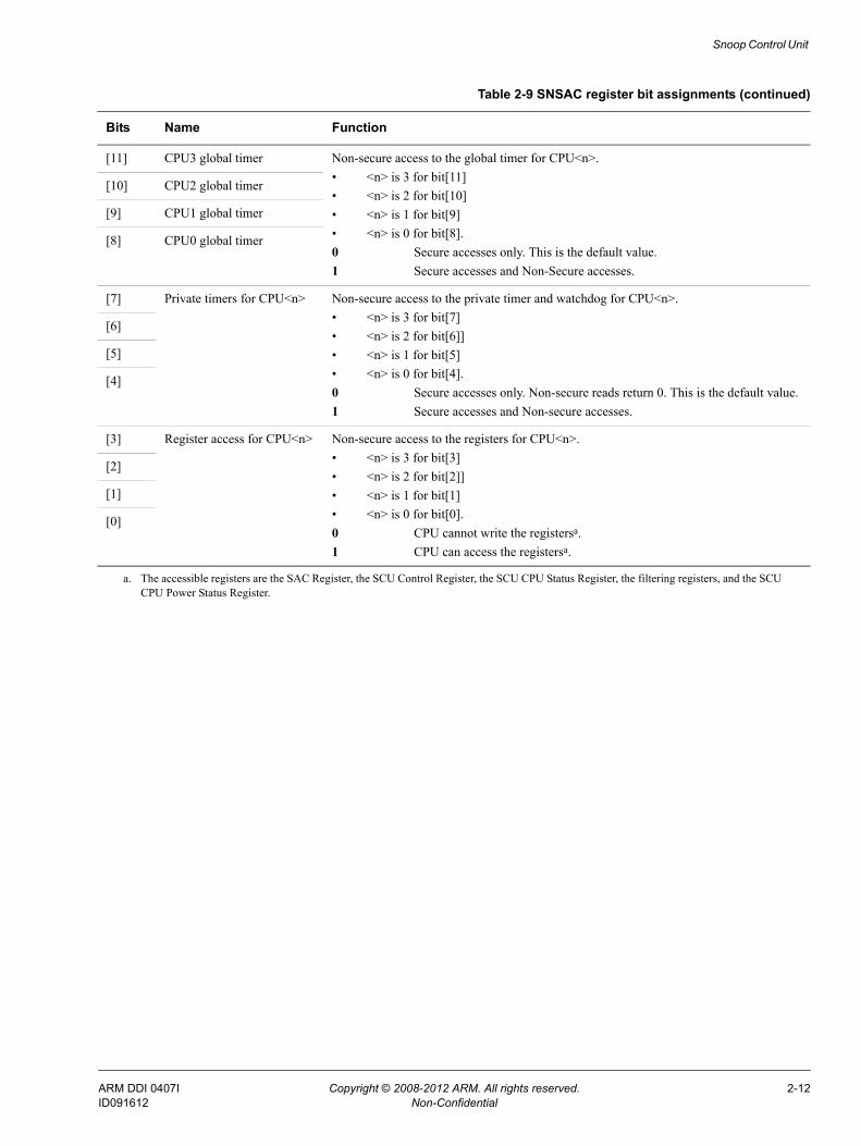
Snoop Control Unit
[11] CPU3 global timer Non-secure access to the global timer for CPU<n>. • <n> is 3 for bit[11] • <n> is 2 for bit[10]• <n> is 1 for bit[9] • <n> is 0 for bit[8]. 0 Secure accesses only. This is the default value.1 Secure accesses and Non-Secure accesses.
[10] CPU2 global timer
[9] CPU1 global timer
[8] CPU0 global timer
[7] Private timers for CPU<n> Non-secure access to the private timer and watchdog for CPU<n>. • <n> is 3 for bit[7] • <n> is 2 for bit[6]]• <n> is 1 for bit[5] • <n> is 0 for bit[4]. 0 Secure accesses only. Non-secure reads return 0. This is the default value.1 Secure accesses and Non-secure accesses.
[6]
[5]
[4]
[3] Register access for CPU<n> Non-secure access to the registers for CPU<n>.• <n> is 3 for bit[3] • <n> is 2 for bit[2]]• <n> is 1 for bit[1] • <n> is 0 for bit[0]. 0 CPU cannot write the registersa.1 CPU can access the registersa.
[2]
[1]
[0]
a. The accessible registers are the SAC Register, the SCU Control Register, the SCU CPU Status Register, the filtering registers, and the SCU CPU Power Status Register.
Table 2-9 SNSAC register bit assignments (continued)
Bits Name Function
ARM DDI 0407I Copyright © 2008-2012 ARM. All rights reserved. 2-12ID091612 Non-Confidential
Snoop Control Unit
2.3 AMBA AXI Master Port InterfacesThe following sections describe the AMBA AXI interfaces:• AXI issuing capabilities• Cortex-A9 MPCore AXI transactions on page 2-14• AXI transaction IDs on page 2-14• AXI USER attributes encodings on page 2-15• Address filtering capabilities on page 2-17.• AXI master interface clocking on page 2-18.• ACP interface clocking on page 2-21.
2.3.1 AXI issuing capabilities
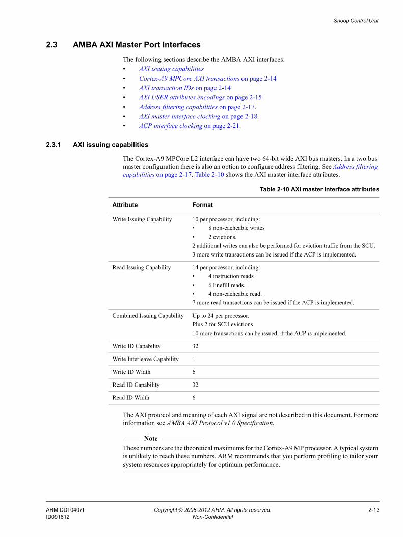
The Cortex-A9 MPCore L2 interface can have two 64-bit wide AXI bus masters. In a two bus master configuration there is also an option to configure address filtering. See Address filtering capabilities on page 2-17. Table 2-10 shows the AXI master interface attributes.
The AXI protocol and meaning of each AXI signal are not described in this document. For more information see AMBA AXI Protocol v1.0 Specification.
Note These numbers are the theoretical maximums for the Cortex-A9 MP processor. A typical system is unlikely to reach these numbers. ARM recommends that you perform profiling to tailor your system resources appropriately for optimum performance.
Table 2-10 AXI master interface attributes
Attribute Format
Write Issuing Capability 10 per processor, including: • 8 non-cacheable writes • 2 evictions.2 additional writes can also be performed for eviction traffic from the SCU.3 more write transactions can be issued if the ACP is implemented.
Read Issuing Capability 14 per processor, including: • 4 instruction reads • 6 linefill reads.• 4 non-cacheable read.7 more read transactions can be issued if the ACP is implemented.
Combined Issuing Capability Up to 24 per processor.Plus 2 for SCU evictions10 more transactions can be issued, if the ACP is implemented.
Write ID Capability 32
Write Interleave Capability 1
Write ID Width 6
Read ID Capability 32
Read ID Width 6
ARM DDI 0407I Copyright © 2008-2012 ARM. All rights reserved. 2-13ID091612 Non-Confidential
Snoop Control Unit
2.3.2 Cortex-A9 MPCore AXI transactions
Cortex-A9 MPCore contains up to four individual Cortex-A9 processors that can generate only a subset of all AXI transactions as described in the Cortex-A9 Technical Reference Manual. As a consequence, only this subset of AXI transactions can appear on the Cortex-A9 MPCore master ports.
However, when the ACP is implemented, ACP traffic can generate transactions not defined in this list.
2.3.3 AXI transaction IDs
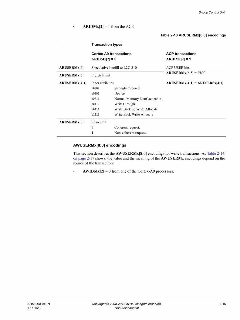
There are several possible sources for the AXI transactions a Cortex-A9MP processor issues on its AXI master ports. This section describes the AXI transaction IDs and AXI USER bits in the following sections:• ARIDMx[5:0] encodings• AWIDMx[5:0] encodings on page 2-15.• ARUSERMx[6:0] encodings on page 2-15• AWUSERMx[8:0] encodings on page 2-16.
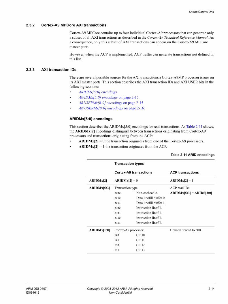
ARIDMx[5:0] encodings
This section describes the ARIDMx[5:0] encodings for read transactions. As Table 2-11 shows, the ARIDMx[2] encodings distinguish between transactions originating from Cortex-A9 processors and transactions originating from the ACP:• ARIDMx[2] = 0 the transaction originates from one of the Cortex-A9 processors.• ARIDMx[2] = 1 the transaction originates from the ACP.
Table 2-11 ARID encodings
Transaction types
Cortex-A9 transactions ACP transactions
ARIDMx[2] ARIDMx[2] = 0 ARIDMx[2] = 1
ARIDMx[5:3] Transaction type:b000 Non-cacheable.b010 Data linefill buffer 0.b011 Data linefill buffer 1.b100 Instruction linefill.b101 Instruction linefill.b110 Instruction linefill.b111 Instruction linefill.
ACP read IDs ARIDMx[5:3] = ARIDS[2:0]
ARIDMx[1:0] Cortex-A9 processor:b00 CPU0.b01 CPU1.b10 CPU2.b11 CPU3.
Unused, forced to b00.
ARM DDI 0407I Copyright © 2008-2012 ARM. All rights reserved. 2-14ID091612 Non-Confidential
Snoop Control Unit
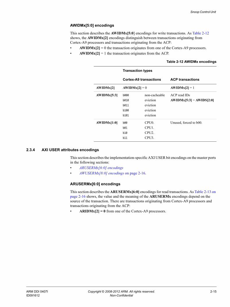
AWIDMx[5:0] encodings
This section describes the AWIDMx[5:0] encodings for write transactions. As Table 2-12 shows, the AWIDMx[2] encodings distinguish between transactions originating from Cortex-A9 processors and transactions originating from the ACP:• AWIDMx[2] = 0 the transaction originates from one of the Cortex-A9 processors.• AWIDMx[2] = 1 the transaction originates from the ACP.
2.3.4 AXI USER attributes encodings
This section describes the implementation-specific AXI USER bit encodings on the master ports in the following sections:• ARUSERMx[6:0] encodings• AWUSERMx[8:0] encodings on page 2-16.
ARUSERMx[6:0] encodings
This section describes the ARUSERMx[6:0] encodings for read transactions. As Table 2-13 on page 2-16 shows, the value and the meaning of the ARUSERMx encodings depend on the source of the transaction. There are transactions originating from Cortex-A9 processors and transactions originating from the ACP:• ARIDMx[2] = 0 from one of the Cortex-A9 processors.
Table 2-12 AWIDMx encodings
Transaction types
Cortex-A9 transactions ACP transactions
AWIDMx[2] AWIDMx[2] = 0 AWIDMx[2] = 1
AWIDMx[5:3] b000 non-cacheableb010 evictionb011 evictionb100 evictionb101 eviction
ACP read IDs AWIDMx[5:3] = AWIDS[2:0]
AWIDMx[1:0] b00 CPU0.b01 CPU1.b10 CPU2.b11 CPU3.
Unused, forced to b00.
ARM DDI 0407I Copyright © 2008-2012 ARM. All rights reserved. 2-15ID091612 Non-Confidential
Snoop Control Unit
• ARIDMx[2] = 1 from the ACP.
AWUSERMx[8:0] encodings
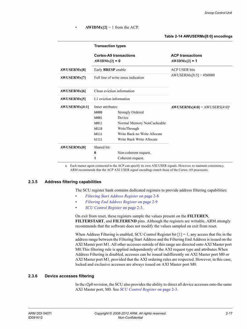
This section describes the AWUSERMx[8:0] encodings for write transactions. As Table 2-14 on page 2-17 shows, the value and the meaning of the AWUSERMx encodings depend on the source of the transaction:
• AWIDMx[2] = 0 from one of the Cortex-A9 processors.
Table 2-13 ARUSERMx[6:0] encodings
Transaction types
Cortex-A9 transactionsARIDMx[2] = 0
ACP transactionsARIDMx[2] = 1
ARUSERMx[6] Speculative linefill to L2C-310 ACP USER bits ARUSERMx[6:5] = 2'b00
ARUSERMx[5] Prefetch hint
ARUSERMx[4:1] Inner attributesb0000 Strongly Orderedb0001 Deviceb0011 Normal Memory NonCacheableb0110 WriteThroughb0111 Write Back no Write Allocateb1111 Write Back Write Allocate
ARUSERMx[4:1] = ARUSERSx[4:1]
ARUSERMx[0] Shared bit0 Coherent request.1 Non-coherent request.
ARM DDI 0407I Copyright © 2008-2012 ARM. All rights reserved. 2-16ID091612 Non-Confidential
Snoop Control Unit
• AWIDMx[2] = 1 from the ACP.
2.3.5 Address filtering capabilities
The SCU register bank contains dedicated registers to provide address filtering capabilities:• Filtering Start Address Register on page 2-8• Filtering End Address Register on page 2-9• SCU Control Register on page 2-3.
On exit from reset, these registers sample the values present on the FILTEREN, FILTERSTART, and FILTEREND pins. Although the registers are writable, ARM strongly recommends that the software does not modify the values sampled on exit from reset.
When Address Filtering is enabled, SCU Control Register bit [1] = 1, any access that fits in the address range between the Filtering Start Address and the Filtering End Address is issued on the AXI Master port M1. All other accesses outside of this range are directed onto AXI Master port M0.This filtering rule is applied independently of the AXI request type and attributes.When Address Filtering is disabled, accesses can be issued indifferently on AXI Master port M0 or AXI Master port M1, provided that the AXI ordering rules are respected. However, in this case, locked and exclusive accesses are always issued on AXI Master port M0.
2.3.6 Device accesses filtering
In the r2p0 revision, the SCU also provides the ability to direct all device accesses onto the same AXI Master port, M0. See SCU Control Register on page 2-3.
Table 2-14 AWUSERMx[8:0] encodings
Transaction types
Cortex-A9 transactionsAWIDMx[2] = 0
ACP transactionsAWIDMx[2] = 1
AWUSERMx[8] Early BRESP enable ACP USER bits AWUSERMx[8:5] = 4'b0000
AWUSERMx[7] Full line of write zeros indication
AWUSERMx[6] Clean eviction information
AWUSERMx[5] L1 eviction information
AWUSERMx[4:1] Inner attributes:b0000 Strongly Orderedb0001 Deviceb0011 Normal Memory NonCacheableb0110 WriteThroughb0111 Write Back no Write Allocateb1111 Write Back Write Allocate
AWUSERMx[4:0] = AWUSERS[4:0]a
AWUSERMx[0] Shared bit:0 Non-coherent request.1 Coherent request.
a. Each master agent connected to the ACP can specify its own AXI USER signals. However, to maintain consistency, ARM recommends that the ACP AXI USER signal encodings match those of the Cortex-A9 processors.
ARM DDI 0407I Copyright © 2008-2012 ARM. All rights reserved. 2-17ID091612 Non-Confidential
Snoop Control Unit
This feature can be used in systems where slow device traffic is expected. Directing all device traffic on the same AXI Master port M0 ensures that the other AXI Master port M1 remains available for other traffic types, cacheable traffic for example.
Note The Address Filtering capabilities take precedence over the Force Device to AXI Master port M0 feature. That is, when address filtering is enabled, a device access falling in the Address Filtering range is issued onto AXI Master port M1 even if SCU Control Register bit[1] is set.
2.3.7 AXI master interface clocking
The Cortex-A9 MPCore Bus Interface Unit supports the following AXI bus ratios relative to CLK:• Integer ratios through clock enable: 1:1, 2:1, 3:1, …• Half-integer ratios through clock enable: 1.5, 2.5 and 3.5 ratios.
In all cases AXI transfers remain synchronous. There is no requirement for an asynchronous AXI interface with integer and half integer ratios. The ratios are configured through external pins, with the following signals that qualify the input and output signals on AXI:• INCLKENM0 and OUTCLKENM0 • INCLKENM1 and OUTCLKENM1.
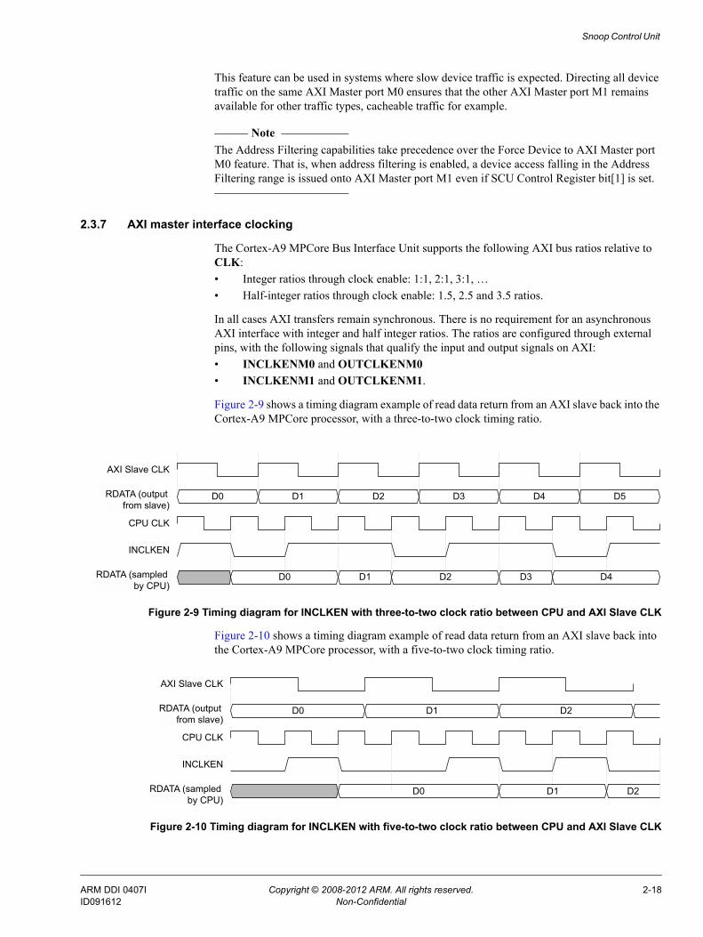
Figure 2-9 shows a timing diagram example of read data return from an AXI slave back into the Cortex-A9 MPCore processor, with a three-to-two clock timing ratio.
Figure 2-9 Timing diagram for INCLKEN with three-to-two clock ratio between CPU and AXI Slave CLK
Figure 2-10 shows a timing diagram example of read data return from an AXI slave back into the Cortex-A9 MPCore processor, with a five-to-two clock timing ratio.
Figure 2-10 Timing diagram for INCLKEN with five-to-two clock ratio between CPU and AXI Slave CLK
CPU CLK
AXI Slave CLK
INCLKEN
RDATA (output from slave)
RDATA (sampled by CPU)
D0 D1 D2 D3 D4 D5
D0 D1 D2 D3 D4
CPU CLK
AXI Slave CLK
INCLKEN
RDATA (output from slave)
RDATA (sampled by CPU)
D0 D1 D2
D0 D1 D2
ARM DDI 0407I Copyright © 2008-2012 ARM. All rights reserved. 2-18ID091612 Non-Confidential
Snoop Control Unit
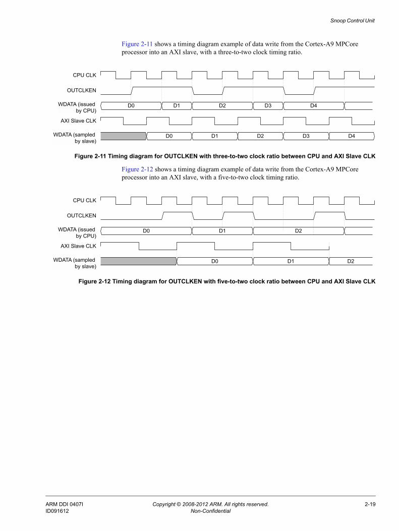
Figure 2-11 shows a timing diagram example of data write from the Cortex-A9 MPCore processor into an AXI slave, with a three-to-two clock timing ratio.
Figure 2-11 Timing diagram for OUTCLKEN with three-to-two clock ratio between CPU and AXI Slave CLK
Figure 2-12 shows a timing diagram example of data write from the Cortex-A9 MPCore processor into an AXI slave, with a five-to-two clock timing ratio.
Figure 2-12 Timing diagram for OUTCLKEN with five-to-two clock ratio between CPU and AXI Slave CLK
CPU CLK
AXI Slave CLK
OUTCLKEN
WDATA (sampled by slave)
WDATA (issued by CPU)
D0 D1 D2 D3 D4
D0 D1 D2 D3 D4
CPU CLK
AXI Slave CLK
OUTCLKEN
WDATA (sampled by slave)
WDATA (issued by CPU)
D0 D1
D0 D1 D2
D2
ARM DDI 0407I Copyright © 2008-2012 ARM. All rights reserved. 2-19ID091612 Non-Confidential
Snoop Control Unit
2.4 Accelerator Coherency PortThe Accelerator Coherency Port (ACP) is an optional AXI 64-bit slave port that can be connected to non-cached AXI master peripherals, such as a DMA engine or cryptographic engine.
This AMBA 3 AXI compatible slave interface on the SCU provides an interconnect point for a range of system masters that for overall system performance, power consumption or reasons of software simplification, are better interfaced directly with the Cortex-A9 MPCore processor. ACP interface clocking on page 2-21 describes ACP timing.
The following sections describe the ACP:• ACP requests• ACP interface clocking on page 2-21• ACP limitations on page 2-21.
2.4.1 ACP requests
The read and write requests performed on the ACP behave differently depending on whether the request is coherent or not. ACP requests behavior is as follows:
ACP coherent read requests An ACP read request is coherent when ARUSER[0] = 1 and ARCACHE[1] = 1 alongside ARVALID.In this case, the SCU enforces coherency. When the data is present in one of the Cortex-A9 processors within the Cortex-A9MPCore, the data is read directly from the relevant processor, and returned to the ACP port.When the data is not present in any of the Cortex-A9 processors, the read request is issued on one of the Cortex-A9 MPCore AXI master ports, along with all its AXI parameters, with the exception of the locked attribute.
ACP non-coherent read requests An ACP read request is non-coherent when ARUSER[0] = 0 or ARCACHE[1] =0 alongside ARVALID.In this case, the SCU does not enforces coherency, and the read request is directly forwarded to one of the available Cortex-A9 MPCore AXI master ports.
ACP coherent write requests An ACP write request is coherent when AWUSER[0] = 1 and AWCACHE[1] =1 alongside AWVALID.In this case, the SCU enforces coherency.When the data is present in one of the Cortex-A9 processors within the Cortex-A9 MPCore, the data is first cleaned and invalidated from the relevant CPU.When the data is not present in any of the Cortex-A9 processors, or when it has been cleaned and invalidated, the write request is issued on one of the Cortex-A9 MPCore AXI master ports, along with all corresponding AXI parameters with the exception of the locked attribute.
ARM DDI 0407I Copyright © 2008-2012 ARM. All rights reserved. 2-20ID091612 Non-Confidential
Snoop Control Unit
Note The transaction can optionally allocate into the L2 cache if the write
parameters are set accordingly.
ACP non-coherent write requests An ACP write request is non-coherent when AWUSER[0] = 0 or AWCACHE[1] = 0 alongside AWVALID.In this case, the SCU does not enforce coherency, and the write request is forwarded directly to one of the available Cortex-A9 MPCore AXI master ports.
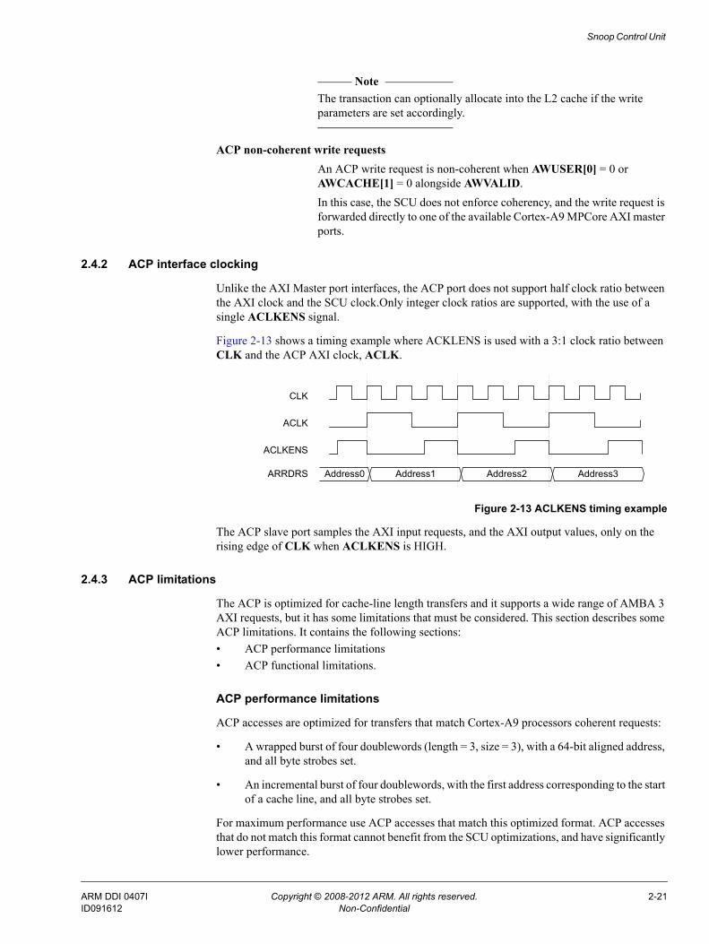
2.4.2 ACP interface clocking
Unlike the AXI Master port interfaces, the ACP port does not support half clock ratio between the AXI clock and the SCU clock.Only integer clock ratios are supported, with the use of a single ACLKENS signal.
Figure 2-13 shows a timing example where ACKLENS is used with a 3:1 clock ratio between CLK and the ACP AXI clock, ACLK.
Figure 2-13 ACLKENS timing example
The ACP slave port samples the AXI input requests, and the AXI output values, only on the rising edge of CLK when ACLKENS is HIGH.
2.4.3 ACP limitations
The ACP is optimized for cache-line length transfers and it supports a wide range of AMBA 3 AXI requests, but it has some limitations that must be considered. This section describes some ACP limitations. It contains the following sections:• ACP performance limitations• ACP functional limitations.
ACP performance limitations
ACP accesses are optimized for transfers that match Cortex-A9 processors coherent requests:
• A wrapped burst of four doublewords (length = 3, size = 3), with a 64-bit aligned address, and all byte strobes set.
• An incremental burst of four doublewords, with the first address corresponding to the start of a cache line, and all byte strobes set.
For maximum performance use ACP accesses that match this optimized format. ACP accesses that do not match this format cannot benefit from the SCU optimizations, and have significantly lower performance.
Address1 Address2 Address3
CLK
ACLK
ACLKENS
ARRDRS Address0
ARM DDI 0407I Copyright © 2008-2012 ARM. All rights reserved. 2-21ID091612 Non-Confidential
Snoop Control Unit
ACP functional limitations
The ACP is a full AMBA 3 AXI slave component, with the exception of the following transfers that are not supported:• Exclusive read and write transactions to coherent memory• All locked transactions, except SWP style transactions to non-coherent memory regions.
An SWP style transaction is a locked read access to non-coherent memory, followed by a write access to the same address, and with the same attributes.
• Optimized coherent read and write transfers when byte strobes are not all set.
As a consequence, it is not possible to use the LDREX/STREX mechanism through the ACP to gain exclusive access to coherent memory regions, that are marked with AxUSER[0] = 1 and AxCACHE[1] = 1.
However, the LDREX/STREX mechanism is fully supported through the ACP for non-coherent memory regions, marked with AxUSER[0] = 0 or AxCACHE[1] =0.
ARM DDI 0407I Copyright © 2008-2012 ARM. All rights reserved. 2-22ID091612 Non-Confidential
Snoop Control Unit
2.5 Event communication with an external agent using WFE/SEVA peripheral connected on the coherency port or any other external agent can participate in the WFE/SEV event communication of the Cortex-A9 MPCore processor by using the EVENTI pin. When this pin is asserted, it sends an event message to all the Cortex-A9 processors in the cluster. This is similar to executing a SEV instruction on one processor of the cluster. This enables the external agent to signal to the processors that it has released a semaphore and that the processors can leave the power saving mode. The EVENTI input pin must remain high at least one CPUCLK clock cycle to be visible by the processors.
The external agent can see that at least one of the Cortex-A9 processors in the cluster has executed an SEV instruction by checking the EVENTO pin. This pin is set high for one CLK clock cycle when any of the Cortex-A9 processor in the cluster executes an SEV instruction.
ARM DDI 0407I Copyright © 2008-2012 ARM. All rights reserved. 2-23ID091612 Non-Confidential
Chapter 3 Interrupt Controller
The Interrupt Controller is compliant with the ARM Generic Interrupt Controller Architecture Specification 1.0. This chapter describes the implementation-defined features of the Interrupt Controller. It does not reproduce information already in the ARM Generic Interrupt Controller Architecture Specification. The chapter contains the following sections:• About the Interrupt Controller on page 3-2• Security extensions support on page 3-4• Distributor register descriptions on page 3-5• Interrupt interface register descriptions on page 3-13.
ARM DDI 0407I Copyright © 2008-2012 ARM. All rights reserved. 3-1ID091612 Non-Confidential

Interrupt Controller
3.1 About the Interrupt ControllerThe Interrupt Controller is a single functional unit that is located in a Cortex-A9 MPCore design. It is responsible for centralizing all interrupt sources before dispatching them to each individual Cortex-A9 processor. There is one interrupt interface per Cortex-A9 processor.
The Interrupt Controller is memory-mapped. The Cortex-A9 processors access it by using a private interface through the SCU. See Private Memory Region on page 1-7.
3.1.1 Interrupt Controller Clock frequency
The clock period is configured, during integration, as a multiple of the MPCore clock period. This multiple, N, must be greater than or equal to two. As a consequence, the minimum pulse width of signals driving external interrupt lines is N Cortex-A9 processor clock cycles. See Chapter 5 Clocks, Resets, and Power Management for a description of PERIPHCLK and PERIPHCLKEN.
The timers and watchdogs use the same clock as the interrupt controller.
3.1.2 Interrupt Distributor interrupt sources
Interrupt sources for the Interrupt Distributor are of the following types:
Software Generated Interrupts (SGI) Each Cortex-A9 processor has private interrupts, ID0-ID15, that can only be triggered by software. These interrupts are aliased so that there is no requirement for a requesting Cortex-A9 processor to determine its own CPU ID when it deals with SGIs. The priority of an SGI depends on the value set by the receiving Cortex-A9 processor in the banked SGI priority registers, not the priority set by the sending Cortex-A9 processor.
Global timer, PPI(0) The global timer uses ID27.
A legacy nFIQ pin, PPI(1) In legacy FIQ mode the legacy nFIQ pin, on a per Cortex-A9 processor basis, bypasses the interrupt distributor logic and directly drives interrupt requests into the Cortex-A9 processor. When a Cortex-A9 processor uses the Interrupt Controller, rather than the legacy pin in the legacy mode, by enabling its own Cortex-A9 processor interface, the legacy nFIQ pin is treated like other interrupt lines and uses ID28.
Private timer, PPI(2) Each Cortex-A9 processor has its own private timers that can generate interrupts, using ID29.
Watchdog timers, PPI(3) Each Cortex-A9 processor has its own watchdog timers that can generate interrupts, using ID30.
A legacy nIRQ pin, PPI(4) In legacy IRQ mode the legacy nIRQ pin, on a per Cortex-A9 processor basis, bypasses the interrupt distributor logic and directly drives interrupt requests into the Cortex-A9 processor.
ARM DDI 0407I Copyright © 2008-2012 ARM. All rights reserved. 3-2ID091612 Non-Confidential
Interrupt Controller
When a Cortex-A9 processor uses the Interrupt Controller, rather than the legacy pin in the legacy mode, by enabling its own Cortex-A9 processor interface, the legacy nIRQ pin is treated like other interrupt lines and uses ID31.
Shared Peripheral Interrupts (SPI) SPIs are triggered by events generated on associated interrupt input lines. The Interrupt Controller can support up to 224 interrupt input lines. The interrupt input lines can be configured to be edge sensitive (positive edge) or level sensitive (high level). SPIs start at ID32.
A unique ID identifies interrupt sources, except the SGIs that are aliased and identified by CPU source.
All interrupt sources have their own configurable priority.
All interrupt sources, except the SGIs and PPIs, also have their own configurable CPU target list, that is, a list of Cortex-A9 processors where the interrupt is sent when triggered by the Interrupt Distributor.
3.1.3 Interrupt Distributor arbitration
The interrupt distributor centralizes all interrupt sources before dispatching them to each individual Cortex-A9 processor.
The Interrupt Distributor arbitrates in the following priority order:
1. Highest priority interrupts. These have the lowest value in the Interrupt Priority Register (ICDIPTR)
2. For interrupts with the same priority value, the Interrupt Distributor arbitrates on the interrupt ID number. It dispatches the smaller ID number first
3. For aliased SGI with the same priority value and the same ID number, the Interrupt Distributor arbitrates on the source CPU number. It dispatches the smaller CPU number first.
The Interrupt Controller hardware ensures that an interrupt targeted at several Cortex-A9 processors can only be taken by one Cortex-A9 processor at a time.
3.1.4 Cortex-A9 MPCore 1-N interrupt model handling
In systems with two or more processors, if an interrupt is received by more than one processor, the Cortex-A9 MPCore ensures that only one of the processors reads the corresponding interrupt ID. This removes the requirement for a lock on the Interrupt Service Routine.
When accessing the ICCIAR register, other processors then read the spurious ID, or another pending ID.
ARM DDI 0407I Copyright © 2008-2012 ARM. All rights reserved. 3-3ID091612 Non-Confidential
Interrupt Controller
3.2 Security extensions supportThe Interrupt Controller permits all implemented interrupts to be individually defined as Secure or Non-secure.
You can program Secure interrupts to use either the IRQ or FIQ interrupt mechanism of a Cortex-A9 processor through the FIQen bit in the ICPICR Register. Non-secure interrupts are always signalled using the IRQ mechanism of a Cortex-A9 processor.
3.2.1 Priority formats
The Cortex-A9 processor implements a five-bit version of the priority format in the ARM Generic Interrupt Controller Architecture Specification. In Non-secure state only four bits of the priority format are visible.
3.2.2 Using CFGSDISABLE
The Interrupt Controller provides the facility to prevent write accesses to critical configuration registers when you assert CFGSDISABLE. This signal controls write behavior for the secure control registers in the distributor and Cortex-A9 processor interfaces, and the Lockable Shared Peripheral Interrupts (LSPIs) in the Interrupt Controller.
If you use CFGSDISABLE, ARM recommends that you assert CFGSDISABLE during the system boot process, after the software has configured the registers. Ideally, the system must only deassert CFGSDISABLE if a hard reset occurs.
When CFGSDISABLE is HIGH, the Interrupt Controller prevents write accesses to the following registers in the:
Distributor The Secure enable of the ICDDCR.
Secure interrupts defined by LSPI field in the ICDICTR: • Interrupt Security Registers • Interrupt Set-Enable Registers• Interrupt Clear-Enable Registers• Interrupt Set-Pending Registers• Interrupt Clear-Pending Registers • Interrupt Priority Registers• ICDIPTR • Interrupt Configuration Register.
Cortex-A9 interrupt interfaces The ICCICR, except for the EnableNS bit.
After you assert CFGSDISABLE, it changes the register bits to read-only and therefore the behavior of these secure interrupts cannot change, even in the presence of rogue code executing in the secure domain.
ARM DDI 0407I Copyright © 2008-2012 ARM. All rights reserved. 3-4ID091612 Non-Confidential
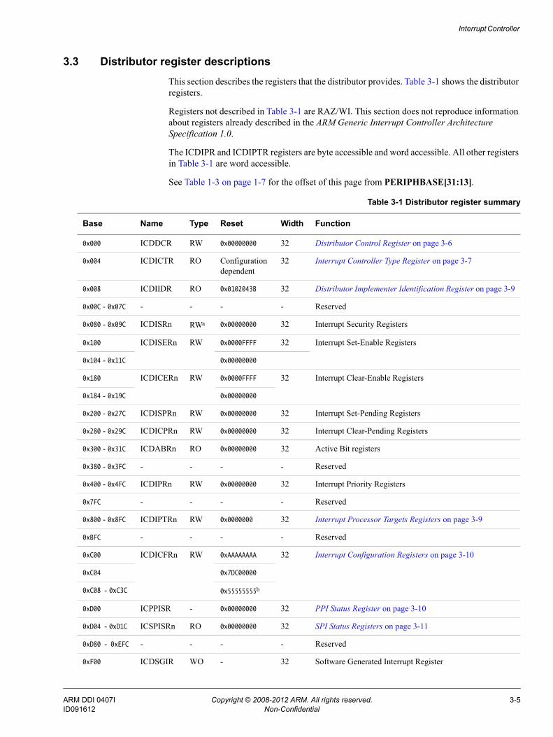
Interrupt Controller
3.3 Distributor register descriptionsThis section describes the registers that the distributor provides. Table 3-1 shows the distributor registers.
Registers not described in Table 3-1 are RAZ/WI. This section does not reproduce information about registers already described in the ARM Generic Interrupt Controller Architecture Specification 1.0.
The ICDIPR and ICDIPTR registers are byte accessible and word accessible. All other registers in Table 3-1 are word accessible.
See Table 1-3 on page 1-7 for the offset of this page from PERIPHBASE[31:13].
Table 3-1 Distributor register summary
Base Name Type Reset Width Function
0x000 ICDDCR RW 0x00000000 32 Distributor Control Register on page 3-6
0x004 ICDICTR RO Configuration dependent
32 Interrupt Controller Type Register on page 3-7
0x008 ICDIIDR RO 0x0102043B 32 Distributor Implementer Identification Register on page 3-9
0x00C - 0x07C - - - - Reserved
0x080 - 0x09C ICDISRn RWa 0x00000000 32 Interrupt Security Registers
0x100 ICDISERn RW 0x0000FFFF 32 Interrupt Set-Enable Registers
0x104 - 0x11C 0x00000000
0x180 ICDICERn RW 0x0000FFFF 32 Interrupt Clear-Enable Registers
0x184 - 0x19C 0x00000000
0x200 - 0x27C ICDISPRn RW 0x00000000 32 Interrupt Set-Pending Registers
0x280 - 0x29C ICDICPRn RW 0x00000000 32 Interrupt Clear-Pending Registers
0x300 - 0x31C ICDABRn RO 0x00000000 32 Active Bit registers
0x380 - 0x3FC - - - - Reserved
0x400 - 0x4FC ICDIPRn RW 0x00000000 32 Interrupt Priority Registers
0x7FC - - - - Reserved
0x800 - 0x8FC ICDIPTRn RW 0x0000000 32 Interrupt Processor Targets Registers on page 3-9
0xBFC - - - - Reserved
0xC00 ICDICFRn RW 0xAAAAAAAA 32 Interrupt Configuration Registers on page 3-10
0xC04 0x7DC00000
0xC08 - 0xC3C 0x55555555b
0xD00 ICPPISR - 0x00000000 32 PPI Status Register on page 3-10
0xD04 - 0xD1C ICSPISRn RO 0x00000000 32 SPI Status Registers on page 3-11
0xD80 - 0xEFC - - - - Reserved
0xF00 ICDSGIR WO - 32 Software Generated Interrupt Register
ARM DDI 0407I Copyright © 2008-2012 ARM. All rights reserved. 3-5ID091612 Non-Confidential
Interrupt Controller
3.3.1 Distributor Control Register
The ICDDCR characteristics are:
Purpose Controls whether the distributor responds to external stimulus changes that occur on SPIs and PPIs.
Usage constraints This register is banked. The register you access depends on the type of access:Secure access Distributor provides access to the Secure Enable and
Non-Secure Enable bits. See Figure 3-1 on page 3-7.Non-secure access Distributor provides access to the Non-Secure enable bit
only. See Figure 3-2 on page 3-7.You cannot modify Enable Secure if CFGSDISABLE is set. You can modify Enable Non-Secure even if CFGSDISABLE is set, through the S or the NS register.
Configurations Available in all Cortex-A9 MPCore configurations.
Attributes See the register summary in Table 3-1 on page 3-5.
Figure 3-1 on page 3-7 shows the ICDDCR bit assignments for Secure accesses.
0xF04 - 0xFCC - - - - Reserved
0xFD0 ICPIDR0 RO 0x4 8 Peripheral ID0 register
0xFD4 ICPIDR1 RO 0x0 8 Peripheral ID1 register
0xFD8 ICPIDR2 RO 0x0 8 Peripheral ID2 register
0xFDC ICPIDR3 RO 0x0 8 Peripheral ID3 register
0xFE0 ICPIDR4 RO 0x90 8 Peripheral ID4 register
0xFE4 ICPIDR5 RO 0xB3 8 Peripheral ID5 register
0xFE8 ICPIDR6 RO 0x1B 8 Peripheral ID6 register
0xFEC ICPIDR7 RO 0x0 8 Peripheral ID7 register
0xFF0 ICCIDR0 RO 0xD 8 Component ID0 register
0xFF4 ICCIDR1 RO 0xF0 8 Component ID1 register
0xFF8 ICCIDR2 RO 0x5 8 Component ID2 register
0xFFC ICCIDR3 RO 0xB1 8 Component ID3 register
a. You must access this register in Secure state.b. Reset value is 0x55555555 when the corresponding interrupts are present, else 0x00000000
Table 3-1 Distributor register summary (continued)
Base Name Type Reset Width Function
ARM DDI 0407I Copyright © 2008-2012 ARM. All rights reserved. 3-6ID091612 Non-Confidential
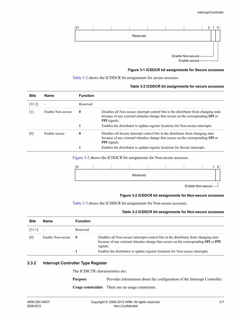
Interrupt Controller
Figure 3-1 ICDDCR bit assignments for Secure accesses
Table 3-2 shows the ICDDCR bit assignments for secure accesses.
Figure 3-2 shows the ICDDCR bit assignments for Non-secure accesses.
Figure 3-2 ICDDCR bit assignments for Non-secure accesses
Table 3-3 shows the ICDDCR bit assignments for Non-secure accesses.
3.3.2 Interrupt Controller Type Register
The ICDICTR characteristics are:
Purpose Provides information about the configuration of the Interrupt Controller.
Usage constraints There are no usage constraints.
31 2 1 0
Enable Non-secureEnable secure
Reserved
Table 3-2 ICDDCR bit assignments for secure accesses
Bits Name Function
[31:2] - Reserved
[1] Enable Non-secure 0 Disables all Non-secure interrupt control bits in the distributor from changing state because of any external stimulus change that occurs on the corresponding SPI or PPI signals.
1 Enables the distributor to update register locations for Non-secure interrupts.
[0] Enable secure 0 Disables all Secure interrupt control bits in the distributor from changing state because of any external stimulus change that occurs on the corresponding SPI or PPI signals.
1 Enables the distributor to update register locations for Secure interrupts.
31 1 0
Enable Non-secure
Reserved
Table 3-3 ICDDCR bit assignments for Non-secure accesses
Bits Name Function
[31:1] - Reserved
[0] Enable Non-secure 0 Disables all Non-secure interrupts control bits in the distributor from changing state because of any external stimulus change that occurs on the corresponding SPI or PPI signals.
1 Enables the distributor to update register locations for Non-secure interrupts.
ARM DDI 0407I Copyright © 2008-2012 ARM. All rights reserved. 3-7ID091612 Non-Confidential
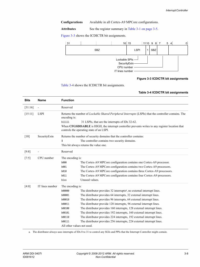
Interrupt Controller
Configurations Available in all Cortex-A9 MPCore configurations.
Attributes See the register summary in Table 3-1 on page 3-5.
Figure 3-3 shows the ICDICTR bit assignments.
Figure 3-3 ICDICTR bit assignments
Table 3-4 shows the ICDICTR bit assignments.
31 0
LSPI SBZ
16
IT lines number
11
SBZ
15 10 9 8 7 5 4
CPU numberSecurityExtn
1
Lockable SPIs
Table 3-4 ICDICTR bit assignments
Bits Name Function
[31:16] - Reserved
[15:11] LSPI Returns the number of Lockable Shared Peripheral Interrupts (LSPIs) that the controller contains. The encoding is:b11111 31 LSPIs, that are the interrupts of IDs 32-62.When CFGSDISABLE is HIGH, the interrupt controller prevents writes to any register location that controls the operating state of an LSPI.
[10] SecurityExtn Returns the number of security domains that the controller contains:1 The controller contains two security domains. This bit always returns the value one.
[9:8] - Reserved
[7:5] CPU number The encoding is:b000 The Cortex-A9 MPCore configuration contains one Cortex-A9 processor.b001 The Cortex-A9 MPCore configuration contains two Cortex-A9 processors.b010 The Cortex-A9 MPCore configuration contains three Cortex-A9 processors.b011 The Cortex-A9 MPCore configuration contains four Cortex-A9 processors.b1xx Unused values.
[4:0] IT lines number The encoding is:b00000 The distributor provides 32 interruptsa, no external interrupt lines.b00001 The distributor provides 64 interrupts, 32 external interrupt lines.b00010 The distributor provides 96 interrupts, 64 external interrupt lines.b00011 The distributor provide 128 interrupts, 96 external interrupt lines.b00100 The distributor provides 160 interrupts, 128 external interrupt lines.b00101 The distributor provides 192 interrupts, 160 external interrupt lines.b00110 The distributor provides 224 interrupts, 192 external interrupt lines.b00111 The distributor provides 256 interrupts, 224 external interrupt lines.All other values not used.
a. The distributor always uses interrupts of IDs 0 to 31 to control any SGIs and PPIs that the Interrupt Controller might contain.
ARM DDI 0407I Copyright © 2008-2012 ARM. All rights reserved. 3-8ID091612 Non-Confidential
Interrupt Controller
3.3.3 Distributor Implementer Identification Register
The ICDIIDR characteristics are:
Purpose Provides information about the implementer and the revision of the controller
Usage constraints There are no usage constraints.
Configurations Available in all Cortex-A9 MPCore configurations.
Attributes See the register summary in Table 3-1 on page 3-5.
Figure 3-4 shows the ICDIIDR bit assignments.
Figure 3-4 ICDIIDR bit assignments
Table 3-5 shows the ICDIIDR bit assignments.
3.3.4 Interrupt Set-Enable Registers
This section describes the implementation defined features of the ICDISERn.
In the Cortex-A9 MPCore, SGIs are always enabled. The corresponding bits in the ICDISERn are read as one, write ignored.
3.3.5 Interrupt Clear-Enable Registers
This section describes the implementation defined features of the ICDICERn.
In the Cortex-A9 MPCore, SGIs are always enabled. The corresponding bits in the ICDICERn are read as one, write ignored.
3.3.6 Interrupt Processor Targets Registers
This section describes the implementation defined features of the ICDIPTRn.
For systems that support only one Cortex-A9 processor, all these registers read as zero, and writes are ignored. The single Cortex-A9 processor is always set as the target of any interruption.
For systems that support two or more Cortex-A9 processors, if the Processor Target field is set to 0 for a specific SPI, then this interrupt cannot be set pending through the hardware pins, nor by a write to the Set-Pending register.
31 24 23 12 11 0
Implementation defined Revision number Implementer
Table 3-5 ICDIIDR bit assignments
Bits Values Name Function
[31:24] 0x01 Implementation version Gives implementation version number.
[23:12] 0x020 Revision number Returns the revision number of the controller.
[11:0] 0x43B Implementer Implementer number.
ARM DDI 0407I Copyright © 2008-2012 ARM. All rights reserved. 3-9ID091612 Non-Confidential
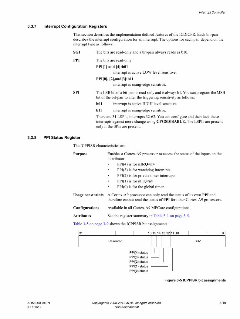
Interrupt Controller
3.3.7 Interrupt Configuration Registers
This section describes the implementation defined features of the ICDICFR. Each bit-pair describes the interrupt configuration for an interrupt. The options for each pair depend on the interrupt type as follows:
SGI The bits are read-only and a bit-pair always reads as b10.
PPI The bits are read-only PPI[1] and [4]:b01
interrupt is active LOW level sensitive.PPI[0], [2],and[3]:b11
interrupt is rising-edge sensitive.
SPI The LSB bit of a bit-pair is read-only and is always b1. You can program the MSB bit of the bit-pair to alter the triggering sensitivity as follows:b01 interrupt is active HIGH level sensitiveb11 interrupt is rising-edge sensitive.There are 31 LSPIs, interrupts 32-62. You can configure and then lock these interrupts against more change using CFGSDISABLE. The LSPIs are present only if the SPIs are present.
3.3.8 PPI Status Register
The ICPPISR characteristics are:
Purpose Enables a Cortex-A9 processor to access the status of the inputs on the distributor: • PPI(4) is for nIRQ<n>• PPI(3) is for watchdog interrupts• PPI(2) is for private timer interrupts• PPI(1) is for nFIQ<n>• PPI(0) is for the global timer.
Usage constraints A Cortex-A9 processor can only read the status of its own PPI and therefore cannot read the status of PPI for other Cortex-A9 processors.
Configurations Available in all Cortex-A9 MPCore configurations.
Attributes See the register summary in Table 3-1 on page 3-5.
Table 3-5 on page 3-9 shows the ICPPISR bit assignments.
Figure 3-5 ICPPISR bit assignments
PPI(1) status
31 16 15 14 13 12 11 0
PPI(2) status PPI(3) status PPI(4) status
Reserved SBZ
PPI(0) status
10
ARM DDI 0407I Copyright © 2008-2012 ARM. All rights reserved. 3-10ID091612 Non-Confidential
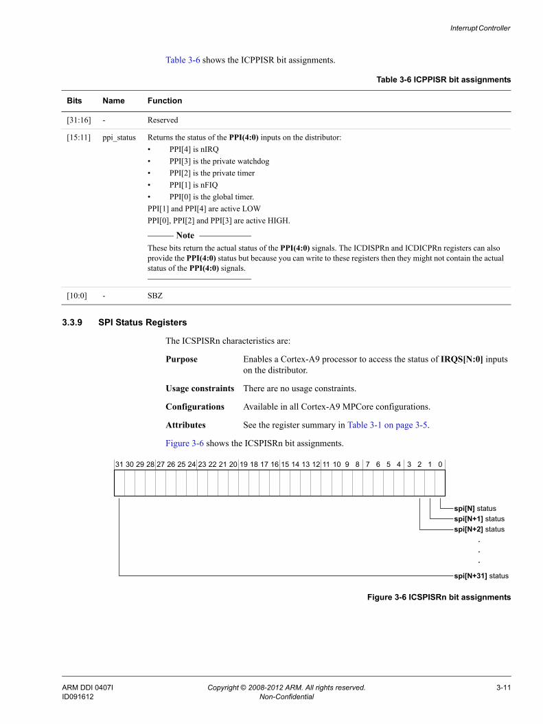
Interrupt Controller
Table 3-6 shows the ICPPISR bit assignments.
3.3.9 SPI Status Registers
The ICSPISRn characteristics are:
Purpose Enables a Cortex-A9 processor to access the status of IRQS[N:0] inputs on the distributor.
Usage constraints There are no usage constraints.
Configurations Available in all Cortex-A9 MPCore configurations.
Attributes See the register summary in Table 3-1 on page 3-5.
Figure 3-6 shows the ICSPISRn bit assignments.
Figure 3-6 ICSPISRn bit assignments
Table 3-6 ICPPISR bit assignments
Bits Name Function
[31:16] - Reserved
[15:11] ppi_status Returns the status of the PPI(4:0) inputs on the distributor:• PPI[4] is nIRQ• PPI[3] is the private watchdog• PPI[2] is the private timer• PPI[1] is nFIQ• PPI[0] is the global timer.PPI[1] and PPI[4] are active LOWPPI[0], PPI[2] and PPI[3] are active HIGH.
Note These bits return the actual status of the PPI(4:0) signals. The ICDISPRn and ICDICPRn registers can also provide the PPI(4:0) status but because you can write to these registers then they might not contain the actual status of the PPI(4:0) signals.
[10:0] - SBZ
spi[N] status
31 30 29 28 27 26 25 24 23 22 21 20 19 18 17 16 15 14 13 12 11 10 9 8 7 6 5 4 3 2 1 0
.
.
.
spi[N+1] status spi[N+2] status
spi[N+31] status
ARM DDI 0407I Copyright © 2008-2012 ARM. All rights reserved. 3-11ID091612 Non-Confidential
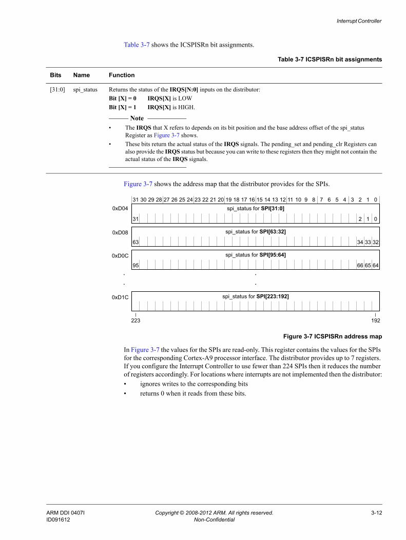
Interrupt Controller
Table 3-7 shows the ICSPISRn bit assignments.
Figure 3-7 shows the address map that the distributor provides for the SPIs.
Figure 3-7 ICSPISRn address map
In Figure 3-7 the values for the SPIs are read-only. This register contains the values for the SPIs for the corresponding Cortex-A9 processor interface. The distributor provides up to 7 registers. If you configure the Interrupt Controller to use fewer than 224 SPIs then it reduces the number of registers accordingly. For locations where interrupts are not implemented then the distributor:• ignores writes to the corresponding bits• returns 0 when it reads from these bits.
Table 3-7 ICSPISRn bit assignments
Bits Name Function
[31:0] spi_status Returns the status of the IRQS[N:0] inputs on the distributor:Bit [X] = 0 IRQS[X] is LOWBit [X] = 1 IRQS[X] is HIGH.
Note • The IRQS that X refers to depends on its bit position and the base address offset of the spi_status
Register as Figure 3-7 shows.• These bits return the actual status of the IRQS signals. The pending_set and pending_clr Registers can
also provide the IRQS status but because you can write to these registers then they might not contain the actual status of the IRQS signals.
31 30 29 28 27 26 25 24 23 22 21 20 19 18 17 16 15 14 13 12 11 10 9 8 7 6 5 4 3 2 1 0spi_status for SPI[31:0]
031 12
spi_status for SPI[63:32]
95
spi_status for SPI[95:64]
646566
spi_status for SPI[223:192]
.
.
192
.
.
0xD08
0xD0C
0xD1C
223
3263 3334
0xD04
ARM DDI 0407I Copyright © 2008-2012 ARM. All rights reserved. 3-12ID091612 Non-Confidential
Interrupt Controller
3.4 Interrupt interface register descriptionsThis section shows the registers that each Cortex-A9 processor interface provides. Table 3-8 shows the Cortex-A9 processor interface registers. This section does not reproduce information about registers already described in the ARM Generic Interrupt Controller Architecture Specification.
3.4.1 CPU Interface Implementer Identification Register
The ICCIIDR Register characteristics are:
Purpose Provides information about the implementer and the revision of the controller.
Usage constraints There are no usage constraints.
Configurations Available in all Cortex-A9 MPCore configurations.
Attributes See the register summary in Table 3-8.
Figure 3-8 shows the ICCIIDR bit assignments.
Figure 3-8 ICCIIDR bit assignments
Table 3-8 Cortex-A9 processor interface register summary
Base Name Type Reset Width Function
0x000 ICCICR RW 0x00000000 32 CPU Interface Control Register
0x004 ICCPMR RW 0x00000000 32 Interrupt Priority Mask Register
0x008 ICCBPR RW 0x2
0x3
32 Binary Point Register
0x00C ICCIAR RO 0x000003FF 32 Interrupt Acknowledge Register
0x010 ICCEOIR WO - 32 End Of Interrupt Register
0x014 ICCRPR RO 0x000000FF 32 Running Priority Register
0x018 ICCHPIR RO 0x000003FF 32 Highest Pending Interrupt Register
0x01Ca ICCABPR RW 0x3 32 Aliased Non-secure Binary Point Register
0xFC ICCIDR RO 0x3901243B 32 CPU Interface Implementer Identification Register
a. This address location is only accessible when the Cortex-A9 processor performs a Secure access.
31 0
Revision number Implementer
20 11
Part number
19 121516
Architecturenumber
ARM DDI 0407I Copyright © 2008-2012 ARM. All rights reserved. 3-13ID091612 Non-Confidential
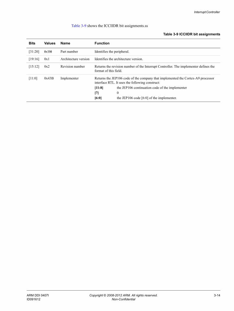
Interrupt Controller
Table 3-9 shows the ICCIIDR bit assignments.ss
Table 3-9 ICCIIDR bit assignments
Bits Values Name Function
[31:20] 0x390 Part number Identifies the peripheral.
[19:16] 0x1 Architecture version Identifies the architecture version.
[15:12] 0x2 Revision number Returns the revision number of the Interrupt Controller. The implementer defines the format of this field.
[11:0] 0x43B Implementer Returns the JEP106 code of the company that implemented the Cortex-A9 processor interface RTL. It uses the following construct:[11:8] the JEP106 continuation code of the implementer[7] 0[6:0] the JEP106 code [6:0] of the implementer.
ARM DDI 0407I Copyright © 2008-2012 ARM. All rights reserved. 3-14ID091612 Non-Confidential
Chapter 4 Global timer, private timers, and watchdog registers
This chapter describes the timers and watchdog registers. It contains the following sections:• About the private timer and watchdog blocks on page 4-2• Private timer and watchdog registers on page 4-3• About the Global Timer on page 4-8• Global timer registers on page 4-9.
ARM DDI 0407I Copyright © 2008-2012 ARM. All rights reserved. 4-1ID091612 Non-Confidential
Global timer, private timers, and watchdog registers
4.1 About the private timer and watchdog blocksThe private timer and watchdog blocks have the following features:• a 32-bit counter that generates an interrupt when it reaches zero• an eight-bit prescaler value to qualify the clock period• configurable single-shot or auto-reload modes• configurable starting values for the counter• the clock for these blocks is PERIPHCLK.
The watchdog can be configured as a timer. See Chapter 5 Clocks, Resets, and Power Management for a description of CLK, PERIPHCLK, and PERIPHCLKEN.
4.1.1 Calculating timer intervals
The timer interval is calculated using the following equation:
This equation can be used to calculate the period between two events generated by a timer or watchdog.
4.1.2 Security extensions
See SCU Non-secure Access Control Register on page 2-11 for information about using timers in Secure or Non-secure state.
PERIPHCLK(PRESCALER_value+1) x (Load_value+1)( )
ARM DDI 0407I Copyright © 2008-2012 ARM. All rights reserved. 4-2ID091612 Non-Confidential
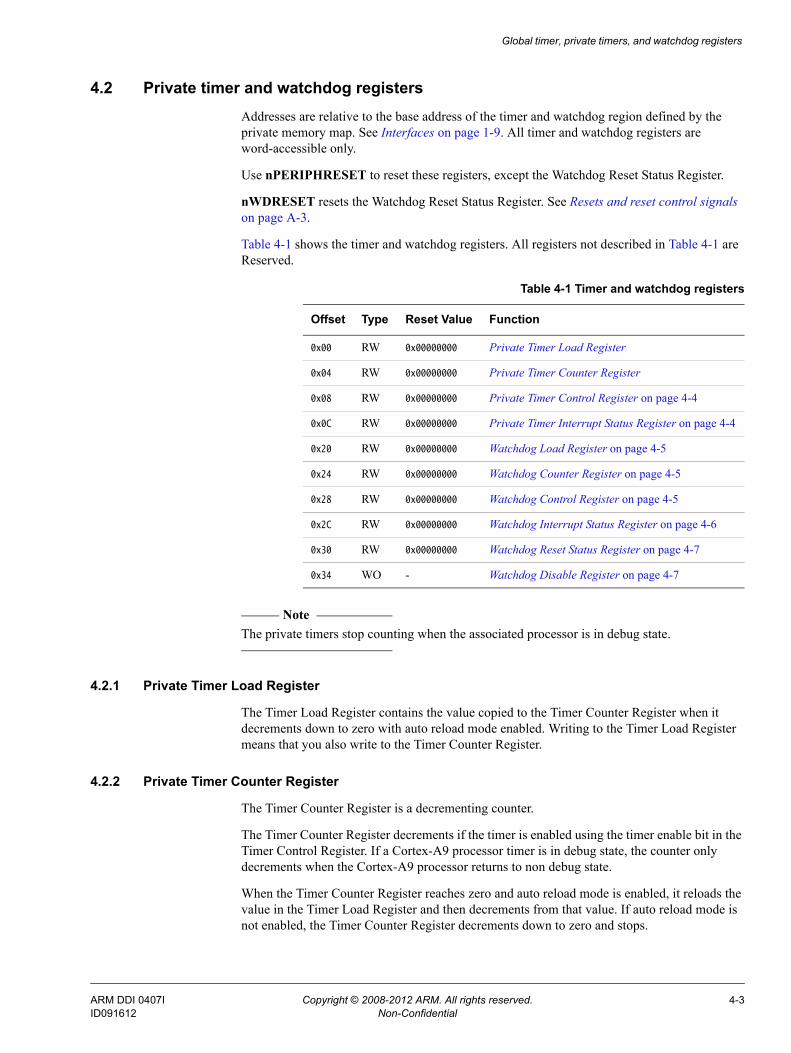
Global timer, private timers, and watchdog registers
4.2 Private timer and watchdog registersAddresses are relative to the base address of the timer and watchdog region defined by the private memory map. See Interfaces on page 1-9. All timer and watchdog registers are word-accessible only.
Use nPERIPHRESET to reset these registers, except the Watchdog Reset Status Register.
nWDRESET resets the Watchdog Reset Status Register. See Resets and reset control signals on page A-3.
Table 4-1 shows the timer and watchdog registers. All registers not described in Table 4-1 are Reserved.
Note The private timers stop counting when the associated processor is in debug state.
4.2.1 Private Timer Load Register
The Timer Load Register contains the value copied to the Timer Counter Register when it decrements down to zero with auto reload mode enabled. Writing to the Timer Load Register means that you also write to the Timer Counter Register.
4.2.2 Private Timer Counter Register
The Timer Counter Register is a decrementing counter.
The Timer Counter Register decrements if the timer is enabled using the timer enable bit in the Timer Control Register. If a Cortex-A9 processor timer is in debug state, the counter only decrements when the Cortex-A9 processor returns to non debug state.
When the Timer Counter Register reaches zero and auto reload mode is enabled, it reloads the value in the Timer Load Register and then decrements from that value. If auto reload mode is not enabled, the Timer Counter Register decrements down to zero and stops.
Table 4-1 Timer and watchdog registers
Offset Type Reset Value Function
0x00 RW 0x00000000 Private Timer Load Register
0x04 RW 0x00000000 Private Timer Counter Register
0x08 RW 0x00000000 Private Timer Control Register on page 4-4
0x0C RW 0x00000000 Private Timer Interrupt Status Register on page 4-4
0x20 RW 0x00000000 Watchdog Load Register on page 4-5
0x24 RW 0x00000000 Watchdog Counter Register on page 4-5
0x28 RW 0x00000000 Watchdog Control Register on page 4-5
0x2C RW 0x00000000 Watchdog Interrupt Status Register on page 4-6
0x30 RW 0x00000000 Watchdog Reset Status Register on page 4-7
0x34 WO - Watchdog Disable Register on page 4-7
ARM DDI 0407I Copyright © 2008-2012 ARM. All rights reserved. 4-3ID091612 Non-Confidential
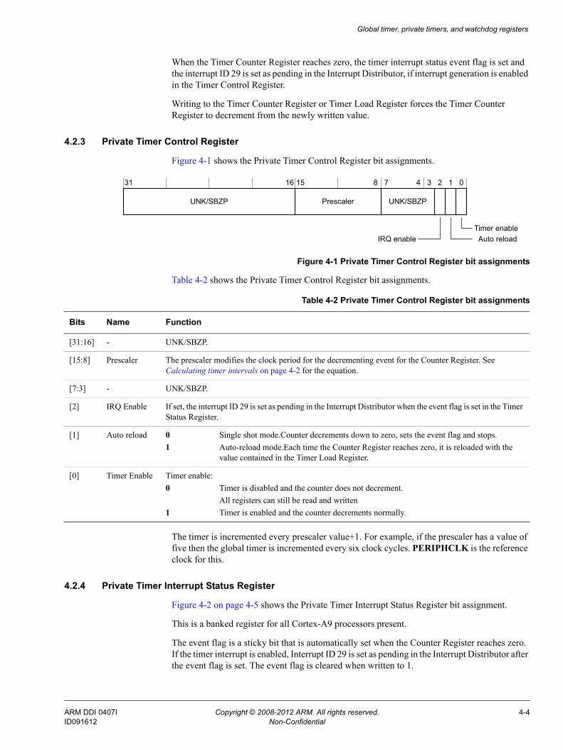
Global timer, private timers, and watchdog registers
When the Timer Counter Register reaches zero, the timer interrupt status event flag is set and the interrupt ID 29 is set as pending in the Interrupt Distributor, if interrupt generation is enabled in the Timer Control Register.
Writing to the Timer Counter Register or Timer Load Register forces the Timer Counter Register to decrement from the newly written value.
4.2.3 Private Timer Control Register
Figure 4-1 shows the Private Timer Control Register bit assignments.
Figure 4-1 Private Timer Control Register bit assignments
Table 4-2 shows the Private Timer Control Register bit assignments.
The timer is incremented every prescaler value+1. For example, if the prescaler has a value of five then the global timer is incremented every six clock cycles. PERIPHCLK is the reference clock for this.
4.2.4 Private Timer Interrupt Status Register
Figure 4-2 on page 4-5 shows the Private Timer Interrupt Status Register bit assignment.
This is a banked register for all Cortex-A9 processors present.
The event flag is a sticky bit that is automatically set when the Counter Register reaches zero. If the timer interrupt is enabled, Interrupt ID 29 is set as pending in the Interrupt Distributor after the event flag is set. The event flag is cleared when written to 1.
UNK/SBZP
31 16 15 8 7 3 2 1 0
UNK/SBZP Prescaler
IRQ enable Auto reloadTimer enable
4
Table 4-2 Private Timer Control Register bit assignments
Bits Name Function
[31:16] - UNK/SBZP.
[15:8] Prescaler The prescaler modifies the clock period for the decrementing event for the Counter Register. See Calculating timer intervals on page 4-2 for the equation.
[7:3] - UNK/SBZP.
[2] IRQ Enable If set, the interrupt ID 29 is set as pending in the Interrupt Distributor when the event flag is set in the Timer Status Register.
[1] Auto reload 0 Single shot mode.Counter decrements down to zero, sets the event flag and stops.1 Auto-reload mode.Each time the Counter Register reaches zero, it is reloaded with the
value contained in the Timer Load Register.
[0] Timer Enable Timer enable:0 Timer is disabled and the counter does not decrement.
All registers can still be read and written1 Timer is enabled and the counter decrements normally.
ARM DDI 0407I Copyright © 2008-2012 ARM. All rights reserved. 4-4ID091612 Non-Confidential
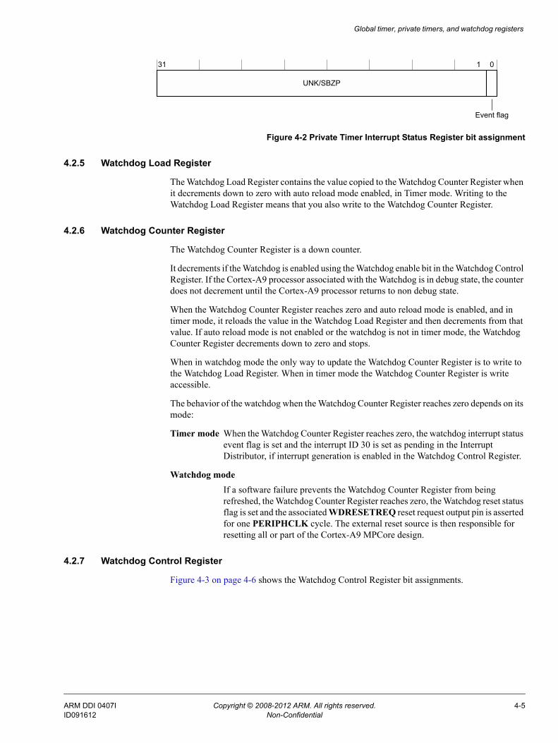
Global timer, private timers, and watchdog registers
Figure 4-2 Private Timer Interrupt Status Register bit assignment
4.2.5 Watchdog Load Register
The Watchdog Load Register contains the value copied to the Watchdog Counter Register when it decrements down to zero with auto reload mode enabled, in Timer mode. Writing to the Watchdog Load Register means that you also write to the Watchdog Counter Register.
4.2.6 Watchdog Counter Register
The Watchdog Counter Register is a down counter.
It decrements if the Watchdog is enabled using the Watchdog enable bit in the Watchdog Control Register. If the Cortex-A9 processor associated with the Watchdog is in debug state, the counter does not decrement until the Cortex-A9 processor returns to non debug state.
When the Watchdog Counter Register reaches zero and auto reload mode is enabled, and in timer mode, it reloads the value in the Watchdog Load Register and then decrements from that value. If auto reload mode is not enabled or the watchdog is not in timer mode, the Watchdog Counter Register decrements down to zero and stops.
When in watchdog mode the only way to update the Watchdog Counter Register is to write to the Watchdog Load Register. When in timer mode the Watchdog Counter Register is write accessible.
The behavior of the watchdog when the Watchdog Counter Register reaches zero depends on its mode:
Timer mode When the Watchdog Counter Register reaches zero, the watchdog interrupt status event flag is set and the interrupt ID 30 is set as pending in the Interrupt Distributor, if interrupt generation is enabled in the Watchdog Control Register.
Watchdog mode If a software failure prevents the Watchdog Counter Register from being refreshed, the Watchdog Counter Register reaches zero, the Watchdog reset status flag is set and the associated WDRESETREQ reset request output pin is asserted for one PERIPHCLK cycle. The external reset source is then responsible for resetting all or part of the Cortex-A9 MPCore design.
4.2.7 Watchdog Control Register
Figure 4-3 on page 4-6 shows the Watchdog Control Register bit assignments.
31 0
UNK/SBZP
Event flag
1
ARM DDI 0407I Copyright © 2008-2012 ARM. All rights reserved. 4-5ID091612 Non-Confidential
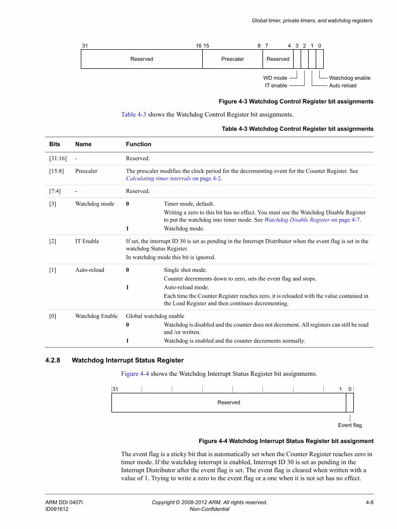
Global timer, private timers, and watchdog registers
Figure 4-3 Watchdog Control Register bit assignments
Table 4-3 shows the Watchdog Control Register bit assignments.
4.2.8 Watchdog Interrupt Status Register
Figure 4-4 shows the Watchdog Interrupt Status Register bit assignments.
Figure 4-4 Watchdog Interrupt Status Register bit assignment
The event flag is a sticky bit that is automatically set when the Counter Register reaches zero in timer mode. If the watchdog interrupt is enabled, Interrupt ID 30 is set as pending in the Interrupt Distributor after the event flag is set. The event flag is cleared when written with a value of 1. Trying to write a zero to the event flag or a one when it is not set has no effect.
Reserved
31 16 15 8 7 4 3 2 1 0
Reserved Prescaler
WD modeIT enable Auto reload
Watchdog enable
Table 4-3 Watchdog Control Register bit assignments
Bits Name Function
[31:16] - Reserved.
[15:8] Prescaler The prescaler modifies the clock period for the decrementing event for the Counter Register. See Calculating timer intervals on page 4-2.
[7:4] - Reserved.
[3] Watchdog mode 0 Timer mode, default.Writing a zero to this bit has no effect. You must use the Watchdog Disable Register to put the watchdog into timer mode. See Watchdog Disable Register on page 4-7.
1 Watchdog mode.
[2] IT Enable If set, the interrupt ID 30 is set as pending in the Interrupt Distributor when the event flag is set in the watchdog Status Register.In watchdog mode this bit is ignored.
[1] Auto-reload 0 Single shot mode.Counter decrements down to zero, sets the event flag and stops.
1 Auto-reload mode.Each time the Counter Register reaches zero, it is reloaded with the value contained in the Load Register and then continues decrementing.
[0] Watchdog Enable Global watchdog enable0 Watchdog is disabled and the counter does not decrement. All registers can still be read
and /or written.1 Watchdog is enabled and the counter decrements normally.
31 0
Reserved
Event flag
1
ARM DDI 0407I Copyright © 2008-2012 ARM. All rights reserved. 4-6ID091612 Non-Confidential
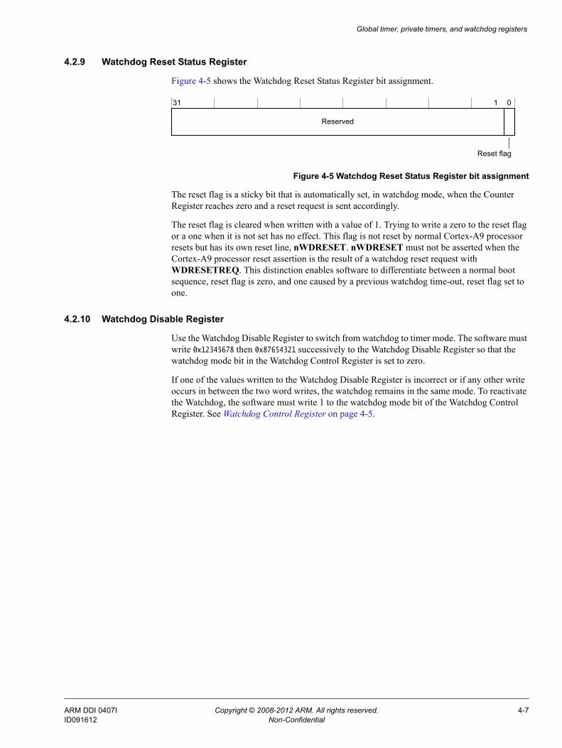
Global timer, private timers, and watchdog registers
4.2.9 Watchdog Reset Status Register
Figure 4-5 shows the Watchdog Reset Status Register bit assignment.
Figure 4-5 Watchdog Reset Status Register bit assignment
The reset flag is a sticky bit that is automatically set, in watchdog mode, when the Counter Register reaches zero and a reset request is sent accordingly.
The reset flag is cleared when written with a value of 1. Trying to write a zero to the reset flag or a one when it is not set has no effect. This flag is not reset by normal Cortex-A9 processor resets but has its own reset line, nWDRESET. nWDRESET must not be asserted when the Cortex-A9 processor reset assertion is the result of a watchdog reset request with WDRESETREQ. This distinction enables software to differentiate between a normal boot sequence, reset flag is zero, and one caused by a previous watchdog time-out, reset flag set to one.
4.2.10 Watchdog Disable Register
Use the Watchdog Disable Register to switch from watchdog to timer mode. The software must write 0x12345678 then 0x87654321 successively to the Watchdog Disable Register so that the watchdog mode bit in the Watchdog Control Register is set to zero.
If one of the values written to the Watchdog Disable Register is incorrect or if any other write occurs in between the two word writes, the watchdog remains in the same mode. To reactivate the Watchdog, the software must write 1 to the watchdog mode bit of the Watchdog Control Register. See Watchdog Control Register on page 4-5.
31 0
Reserved
Reset flag
1
ARM DDI 0407I Copyright © 2008-2012 ARM. All rights reserved. 4-7ID091612 Non-Confidential

Global timer, private timers, and watchdog registers
4.3 About the Global TimerThe global timer has the following features:
• The global timer is a 64-bit incrementing counter with an auto-incrementing feature. It continues incrementing after sending interrupts.
• The global timer is memory mapped in the private memory region. See Private Memory Region on page 1-7.
• The global timer is accessed at reset in Secure State only. See SCU Non-secure Access Control Register on page 2-11.
• The global timer is accessible to all Cortex-A9 processors in the cluster. Each Cortex-A9 processor has a private 64-bit comparator that is used to assert a private interrupt when the global timer has reached the comparator value. All the Cortex-A9 processors in a design use the banked ID, ID27, for this interrupt. ID27 is sent to the Interrupt Controller as a Private Peripheral Interrupt. See Interrupt Distributor interrupt sources on page 3-2.
• The global timer is clocked by PERIPHCLK.
Note • From r2p0 the comparators for each processor with the global timer fire when the timer
value is greater than or equal to. In previous revisions the comparators fired when the timer value was equal to.
• The global timer does not stop counting when any of the processors are in debug state.
ARM DDI 0407I Copyright © 2008-2012 ARM. All rights reserved. 4-8ID091612 Non-Confidential
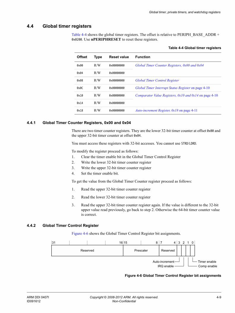
Global timer, private timers, and watchdog registers
4.4 Global timer registersTable 4-4 shows the global timer registers. The offset is relative to PERIPH_BASE_ADDR + 0x0200. Use nPERIPHRESET to reset these registers.
4.4.1 Global Timer Counter Registers, 0x00 and 0x04
There are two timer counter registers. They are the lower 32-bit timer counter at offset 0x00 and the upper 32-bit timer counter at offset 0x04.
You must access these registers with 32-bit accesses. You cannot use STRD/LDRD.
To modify the register proceed as follows:1. Clear the timer enable bit in the Global Timer Control Register2. Write the lower 32-bit timer counter register3. Write the upper 32-bit timer counter register4. Set the timer enable bit.
To get the value from the Global Timer Counter register proceed as follows:
1. Read the upper 32-bit timer counter register
2. Read the lower 32-bit timer counter register
3. Read the upper 32-bit timer counter register again. If the value is different to the 32-bit upper value read previously, go back to step 2. Otherwise the 64-bit timer counter value is correct.
4.4.2 Global Timer Control Register
Figure 4-6 shows the Global Timer Control Register bit assignments.
Figure 4-6 Global Timer Control Register bit assignments
Table 4-4 Global timer registers
Offset Type Reset value Function
0x00 R/W 0x00000000 Global Timer Counter Registers, 0x00 and 0x04
0x04 R/W 0x00000000
0x08 R/W 0x00000000 Global Timer Control Register
0x0C R/W 0x00000000 Global Timer Interrupt Status Register on page 4-10
0x10 R/W 0x00000000 Comparator Value Registers, 0x10 and 0x14 on page 4-10
0x14 R/W 0x00000000
0x18 R/W 0x00000000 Auto-increment Register, 0x18 on page 4-11
Reserved
31 16 15 8 7 3 2 1 0
Reserved Prescaler
IRQ enable Comp enableTimer enable
4
Auto-increment
ARM DDI 0407I Copyright © 2008-2012 ARM. All rights reserved. 4-9ID091612 Non-Confidential
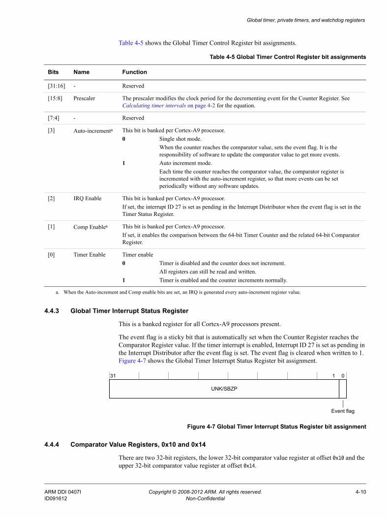
Global timer, private timers, and watchdog registers
Table 4-5 shows the Global Timer Control Register bit assignments.
4.4.3 Global Timer Interrupt Status Register
This is a banked register for all Cortex-A9 processors present.
The event flag is a sticky bit that is automatically set when the Counter Register reaches the Comparator Register value. If the timer interrupt is enabled, Interrupt ID 27 is set as pending in the Interrupt Distributor after the event flag is set. The event flag is cleared when written to 1. Figure 4-7 shows the Global Timer Interrupt Status Register bit assignment.
Figure 4-7 Global Timer Interrupt Status Register bit assignment
4.4.4 Comparator Value Registers, 0x10 and 0x14
There are two 32-bit registers, the lower 32-bit comparator value register at offset 0x10 and the upper 32-bit comparator value register at offset 0x14.
Table 4-5 Global Timer Control Register bit assignments
Bits Name Function
[31:16] - Reserved
[15:8] Prescaler The prescaler modifies the clock period for the decrementing event for the Counter Register. See Calculating timer intervals on page 4-2 for the equation.
[7:4] - Reserved
[3] Auto-incrementa This bit is banked per Cortex-A9 processor.0 Single shot mode.
When the counter reaches the comparator value, sets the event flag. It is the responsibility of software to update the comparator value to get more events.
1 Auto increment mode.Each time the counter reaches the comparator value, the comparator register is incremented with the auto-increment register, so that more events can be set periodically without any software updates.
[2] IRQ Enable This bit is banked per Cortex-A9 processor.If set, the interrupt ID 27 is set as pending in the Interrupt Distributor when the event flag is set in the Timer Status Register.
[1] Comp Enablea This bit is banked per Cortex-A9 processor.If set, it enables the comparison between the 64-bit Timer Counter and the related 64-bit Comparator Register.
[0] Timer Enable Timer enable0 Timer is disabled and the counter does not increment.
All registers can still be read and written.1 Timer is enabled and the counter increments normally.
a. When the Auto-increment and Comp enable bits are set, an IRQ is generated every auto-increment register value.
31 0
UNK/SBZP
Event flag
1
ARM DDI 0407I Copyright © 2008-2012 ARM. All rights reserved. 4-10ID091612 Non-Confidential
Global timer, private timers, and watchdog registers
You must access these registers with 32-bit accesses. You cannot use STRD/LDRD. There is a Comparator Value Register for each Cortex-A9 processor.
To ensure that updates to this register do not set the Interrupt Status Register proceed as follows:1. Clear the Comp Enable bit in the Timer Control Register.2. Write the lower 32-bit Comparator Value Register.3. Write the upper 32-bit Comparator Value Register.4. Set the Comp Enable bit and, if necessary, the IRQ enable bit.
4.4.5 Auto-increment Register, 0x18
This 32-bit register gives the increment value of the Comparator Register when the Auto-increment bit is set in the Timer Control Register. Each Cortex-A9 processor present has its own Auto-increment Register.
If the comp enable and auto-increment bits are set when the global counter reaches the Comparator Register value, the comparator is incremented by the auto-increment value, so that a new event can be set periodically.
The global timer is not affected and goes on incrementing.
ARM DDI 0407I Copyright © 2008-2012 ARM. All rights reserved. 4-11ID091612 Non-Confidential
Chapter 5 Clocks, Resets, and Power Management
This chapter describes the clocks, resets and power management features of the Cortex-A9 MPCore. It contains the following sections:• Clocks on page 5-2• Resets on page 5-3• Power management on page 5-7.
ARM DDI 0407I Copyright © 2008-2012 ARM. All rights reserved. 5-1ID091612 Non-Confidential
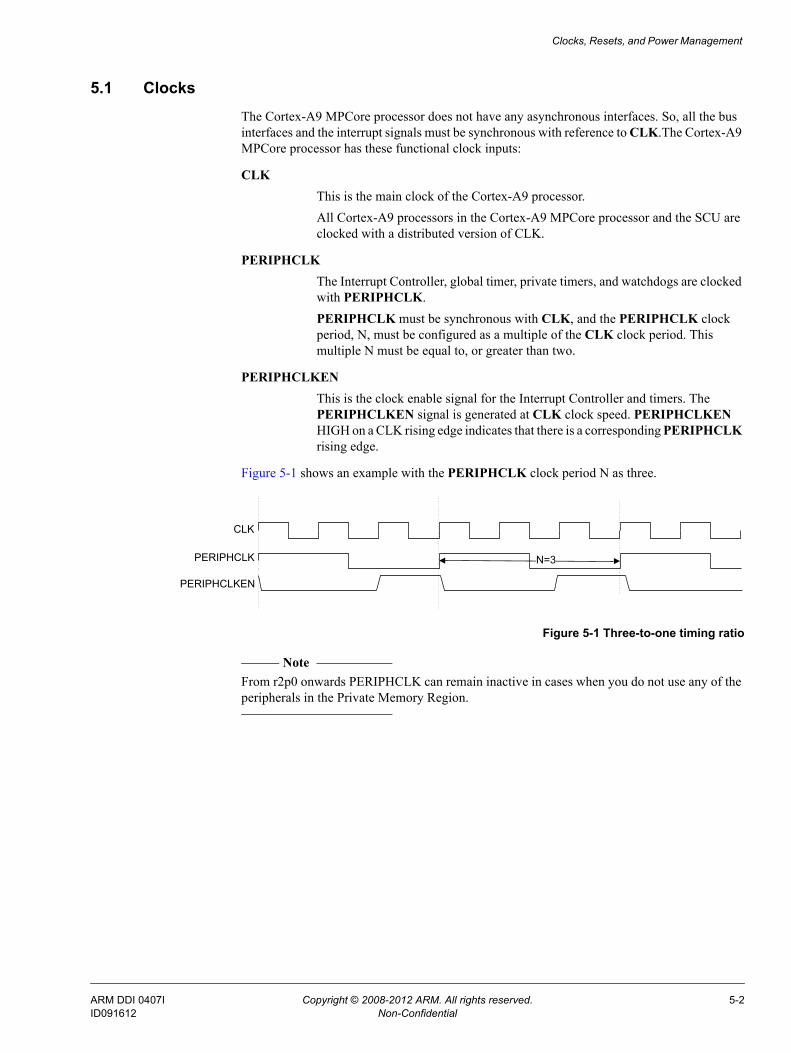
Clocks, Resets, and Power Management
5.1 ClocksThe Cortex-A9 MPCore processor does not have any asynchronous interfaces. So, all the bus interfaces and the interrupt signals must be synchronous with reference to CLK.The Cortex-A9 MPCore processor has these functional clock inputs:
CLK This is the main clock of the Cortex-A9 processor.All Cortex-A9 processors in the Cortex-A9 MPCore processor and the SCU are clocked with a distributed version of CLK.
PERIPHCLK The Interrupt Controller, global timer, private timers, and watchdogs are clocked with PERIPHCLK.PERIPHCLK must be synchronous with CLK, and the PERIPHCLK clock period, N, must be configured as a multiple of the CLK clock period. This multiple N must be equal to, or greater than two.
PERIPHCLKEN This is the clock enable signal for the Interrupt Controller and timers. The PERIPHCLKEN signal is generated at CLK clock speed. PERIPHCLKEN HIGH on a CLK rising edge indicates that there is a corresponding PERIPHCLK rising edge.
Figure 5-1 shows an example with the PERIPHCLK clock period N as three.
Figure 5-1 Three-to-one timing ratio
Note From r2p0 onwards PERIPHCLK can remain inactive in cases when you do not use any of the peripherals in the Private Memory Region.
CLK
PERIPHCLK
PERIPHCLKEN
N=3
ARM DDI 0407I Copyright © 2008-2012 ARM. All rights reserved. 5-2ID091612 Non-Confidential
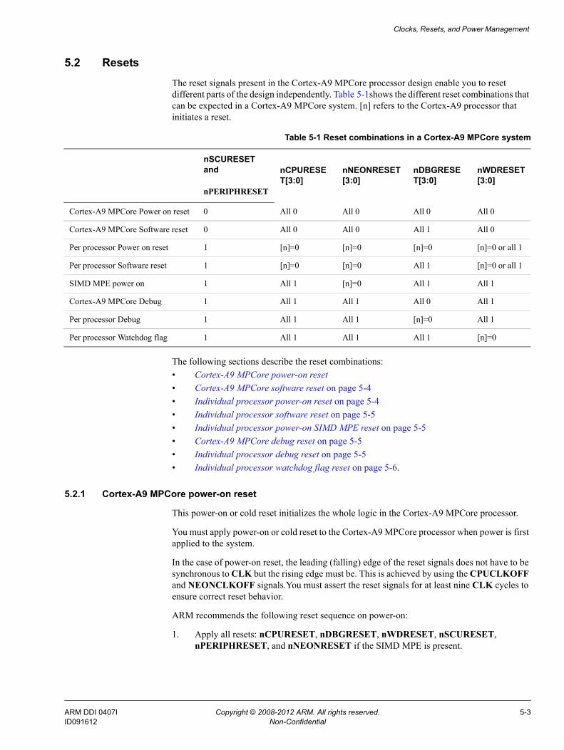
Clocks, Resets, and Power Management
5.2 ResetsThe reset signals present in the Cortex-A9 MPCore processor design enable you to reset different parts of the design independently. Table 5-1shows the different reset combinations that can be expected in a Cortex-A9 MPCore system. [n] refers to the Cortex-A9 processor that initiates a reset.
The following sections describe the reset combinations:• Cortex-A9 MPCore power-on reset• Cortex-A9 MPCore software reset on page 5-4• Individual processor power-on reset on page 5-4• Individual processor software reset on page 5-5• Individual processor power-on SIMD MPE reset on page 5-5• Cortex-A9 MPCore debug reset on page 5-5• Individual processor debug reset on page 5-5• Individual processor watchdog flag reset on page 5-6.
5.2.1 Cortex-A9 MPCore power-on reset
This power-on or cold reset initializes the whole logic in the Cortex-A9 MPCore processor.
You must apply power-on or cold reset to the Cortex-A9 MPCore processor when power is first applied to the system.
In the case of power-on reset, the leading (falling) edge of the reset signals does not have to be synchronous to CLK but the rising edge must be. This is achieved by using the CPUCLKOFF and NEONCLKOFF signals.You must assert the reset signals for at least nine CLK cycles to ensure correct reset behavior.
ARM recommends the following reset sequence on power-on:
1. Apply all resets: nCPURESET, nDBGRESET, nWDRESET, nSCURESET, nPERIPHRESET, and nNEONRESET if the SIMD MPE is present.
Table 5-1 Reset combinations in a Cortex-A9 MPCore system
nSCURESET and nCPURESE
T[3:0]nNEONRESET[3:0]
nDBGRESET[3:0]
nWDRESET[3:0]
nPERIPHRESET
Cortex-A9 MPCore Power on reset 0 All 0 All 0 All 0 All 0
Cortex-A9 MPCore Software reset 0 All 0 All 0 All 1 All 0
Per processor Power on reset 1 [n]=0 [n]=0 [n]=0 [n]=0 or all 1
Per processor Software reset 1 [n]=0 [n]=0 All 1 [n]=0 or all 1
SIMD MPE power on 1 All 1 [n]=0 All 1 All 1
Cortex-A9 MPCore Debug 1 All 1 All 1 All 0 All 1
Per processor Debug 1 All 1 All 1 [n]=0 All 1
Per processor Watchdog flag 1 All 1 All 1 All 1 [n]=0
ARM DDI 0407I Copyright © 2008-2012 ARM. All rights reserved. 5-3ID091612 Non-Confidential
Clocks, Resets, and Power Management
2. Apply at least nine CLK cycles, plus at least one cycle in each other clock domain, or more if the documentation for other components requests it. There is no harm in applying more clock cycles than this, and maximum redundancy can be achieved by applying 15 cycles on every clock domain.
3. Assert all CPUCLKOFF signals with a value of 1’b1 and, if there is an SIMD MPE present, all NEONCLKOFF.
4. Wait for the equivalent of approximately 10 cycles, depending on your implementation. This compensates for clock and reset tree latencies.
5. Release resets.
6. Wait for the equivalent of another approximately 10 cycles, again to compensate for clock and reset tree latencies.
7. Deassert all CPUCLKOFF and NEONCLKOFF. This ensures that all registers in the design see the same CLK edge on exit from the reset sequence.
5.2.2 Cortex-A9 MPCore software reset
This software or warm reset initializes all functional logic in each of the individual Cortex-A9 processor present in the cluster apart from the debug logic.
All breakpoints and watchpoints are retained during this.
ARM recommends that you use the reset sequence in Cortex-A9 MPCore power-on reset on page 5-3, except that nDBGRESET must not be asserted during the sequence. This ensures the debug registers retain their values.
5.2.3 Individual processor power-on reset
This reset initializes the whole logic in a single Cortex-A9 processor, including its debug logic. It is expected to be applied when this individual Cortex-A9 processor exits from power down or dormant state.
This reset only applies to configurations where each individual Cortex-A9 processor is implemented in its own power domain.
The sequence is as follows:
1. Apply nCPURESET[n] and nDBGRESET[n], plus nNEONRESET[n] if the SIMD MPE is present. nWDRESET[n] reset can also be applied optionally if you want to reset the corresponding Watchdog flag.
2. Wait for at least nine CLK cycles, plus at least one cycle in each other clock domain, or more if the documentation for other components requests it. There is no harm in applying more clock cycles than this, and maximum redundancy can be achieved by for example applying 15 cycles on every clock domain.
3. Assert CPUCLKOFF[n] with a value of 1’b1 and, if there is a SIMD MPE present, NEONCLKOFF[n].
4. Wait for the equivalent of approximately 10 cycles, depending on your implementation. This compensates for clock and reset tree latencies.
5. Release all resets.
6. Wait for the equivalent of another approximately 10 cycles, again to compensate for clock and reset tree latencies.
ARM DDI 0407I Copyright © 2008-2012 ARM. All rights reserved. 5-4ID091612 Non-Confidential
Clocks, Resets, and Power Management
7. Deassert CPUCLKOFF[n] and NEONCLKOFF[n]. This ensures that all registers in the processor, and in the SIMD MPE, see the same CLK edge on exit from the reset sequence.
5.2.4 Individual processor software reset
This reset initializes all functional logic in a single Cortex-A9 processor apart from its debug logic.
All breakpoints and watchpoints are retained during this individual warm reset.
This reset only applies to configuration where each individual Cortex-A9 processor is implemented in its own power domain
ARM recommends that you use the reset sequence in Individual processor power-on reset on page 5-4, except that nDBGRESET must not be asserted during the sequence. This ensures the debug registers of the individual processors retain their values
5.2.5 Individual processor power-on SIMD MPE reset
This reset initializes all the SIMD logic of the MPE in a single Cortex-A9 processor.
It is expected to be applied when the SIMD part of the MPE exits from powerdown state.
This reset only applies to configurations where SIMD MPE logic is implemented in its own dedicated power domain, separated from the rest of the processor logic.
ARM recommends the following reset sequence on power-on for an individual CPU SIMD MPE power-on:
1. Apply nNEONRESET[n].
2. Wait for at least nine CLK cycles. There is no harm in applying more clock cycles than this, and maximum redundancy can be achieved by for example applying 15 cycles on every clock domain.
3. Assert NEONCLKOFF[n] with a value of 1’b1.
4. Wait for the equivalent of approximately 10 cycles, depending on your implementation. This compensates for clock and reset tree latencies.
5. Release nNEONRESET[n].
6. Wait for the equivalent of approximately another 10 cycles, again to compensate for clock and reset tree latencies.
7. Deassert NEONCLKOFF[n]. This ensures that all registers in the SIMD MPE part of the processor see the same CLK edge on exit from the reset sequence.
5.2.6 Cortex-A9 MPCore debug reset
This reset initializes the debug logic in all Cortex-A9 processors present in the cluster.
To perform a Cortex-A9 MPCore debug reset, assert all nDBGRESET signals during a few CLK cycles. CPUCLKOFF and NEONCLKOFF must remain deasserted during this reset sequence.
5.2.7 Individual processor debug reset
This reset initializes the debug logic in a single Cortex-A9 processor in the cluster.
ARM DDI 0407I Copyright © 2008-2012 ARM. All rights reserved. 5-5ID091612 Non-Confidential
Clocks, Resets, and Power Management
To perform a Cortex-A9 individual processor debug reset, assert the corresponding nDBGRESET[n] signal during a few CLK cycles. CPUCLKOFF[n] and NEONCLKOFF[n] must remain deasserted during this reset sequence.
5.2.8 Individual processor watchdog flag reset
This reset clears the watchdog flag associated with a single Cortex-A9 processor. Watchdog functionality is independent from all other processor functionality, so this reset is independent from the all other resets.
ARM DDI 0407I Copyright © 2008-2012 ARM. All rights reserved. 5-6ID091612 Non-Confidential

Clocks, Resets, and Power Management
5.3 Power managementThis section describes Cortex-A9MPCore power management. It contains the following sections:• Individual Cortex-A9 processor power management• Communication to the Power Management Controller on page 5-9• Cortex-A9 MPCore power domains on page 5-10• Multiprocessor bring-up on page 5-10.
5.3.1 Individual Cortex-A9 processor power management
Place holders for clamps are inserted around each Cortex-A9 processor so that implementation of different power domains can be eased. It is the responsibility of software to signal to the Snoop Control Unit and the Distributed Interrupt Controller that a Cortex-A9 processor is shut off so that the Cortex-A9 processor can be seen as non-existent in the cluster. Each Cortex-A9 processor can be in one of the following modes:
Run mode Everything is clocked and powered-up
Standby mode The CPU clock is stopped. Only logic required for wake-up is still active.
Dormant mode Everything is powered off except RAM arrays that are in retention mode.
Shutdown Everything is powered-off.
Table 5-2 shows the individual power modes.
Entry to Dormant or powered-off mode must be controlled through an external power controller. The CPU Status Register in the SCU is used in conjunction with CPU WFI entry flag to signal to the power controller the power domain that it can cut, using the PWRCTL bus. See SCU CPU Power Status Register on page 2-6.
Run mode
Run mode is the normal mode of operation, where all of the functionality of the Cortex-A9 processor is available.
Table 5-2 Cortex-A9 MPCore power modes
Mode Cortex-A9 processor logic RAM arrays Wake-up mechanism
Run Mode Powered-upEverything clocked
Powered-up N/A
Standby modes
Powered-upOnly wake-up logic clocked
Powered-up Standard Standby modes wake up events. See Standby modes on page 5-8
Dormant Powered-off Retention state/voltage External wake-up event to power controller, that can perform a reset of the processor.
Shutdown Powered-off Powered-off External wake-up event to power controller, that can perform a reset of the processor.
ARM DDI 0407I Copyright © 2008-2012 ARM. All rights reserved. 5-7ID091612 Non-Confidential
Clocks, Resets, and Power Management
Standby modes
WFI and WFE Standby modes disable most of the clocks in a processor, while keeping its logic powered up. This reduces the power drawn to the static leakage current, leaving a tiny clock power overhead requirement to enable the device to wake up.
Entry into WFI Standby mode is performed by executing the WFI instruction.
The transition from the WFI Standby mode to the Run mode is caused by:• An IRQ interrupt, regardless of the value of the CSPR.I bit.• An FIQ interrupt, regardless of the value of the CSPR.F bit.• An asynchronous abort, regardless of the value of the CPSR.A bit.• A debug event, if invasive debug is enabled and the debug event is permitted.• A CP15 maintenance request broadcast by other processors.
Entry into WFE Standby mode is performed by executing the WFE instruction.
The transition from the WFE Standby mode to the Run mode is caused by:• An IRQ interrupt, unless masked by the CPSR.I bit.• An FIQ interrupt, unless masked by the CPSR.F bit.• An asynchronous abort, unless masked by the CPSR.A bit.• A debug event, if invasive debug is enabled and the debug event is permitted.• The assertion of the EVENTI input signal.• The execution of an SEV instruction on any processor in the multiprocessor system. • A CP15 maintenance request broadcast by other processors.
The debug request can be generated by an externally generated debug request, using the EDBGRQ pin on the Cortex-A9 processor, or from a Debug Halt instruction issued to the Cortex-A9 processor through the APB debug port.
The debug channel remains active throughout a WFI instruction.
Note When a processor in Standby mode receives an SCU coherency request, the clock on its L1 memory system is restored temporarily so that the request can be handled. This mechanism prevents the requirement for a processor about to enter Standby mode from having to flush its L1 data cache by ensuring that its coherent data remain accessible by other processors.
Dormant mode
Dormant mode is designed to enable the Cortex-A9 processor to be powered down, while leaving the caches powered up and maintaining their state.
The RAM blocks that are to remain powered up must be implemented on a separate power domain, and there is a requirement to clamp all of the inputs to the RAMs to a known logic level, with the chip enable being held inactive. This clamping is not implemented in gates as part of the default synthesis flow because it would contribute to a tight critical path. Implementations that want to implement Dormant mode must add these clamps around the RAMs, either as explicit gates in the RAM power domain, or as pull-down transistors that clamp the values while the Cortex-A9 processor is powered down. The RAM blocks that must remain powered up during Dormant mode are:• all Data RAMs associated with the cache• all Tag RAMs associated with the cache
ARM DDI 0407I Copyright © 2008-2012 ARM. All rights reserved. 5-8ID091612 Non-Confidential
Clocks, Resets, and Power Management
Before entering Dormant mode, the state of the Cortex-A9 processor, excluding the contents of the RAMs that remain powered up in dormant mode, must be saved to external memory. These state saving operations must ensure that the following occur:
• All ARM registers, including CPSR and SPSR registers are saved.
• All system registers are saved.
• All debug-related state must be saved.
• the Cortex-A9 processor must correctly set the CPU Status Register in the SCU so that it enters Dormant Mode. See SCU CPU Power Status Register on page 2-6.
• A Data Synchronization Barrier instruction is executed to ensure that all state saving has been completed.
• The Cortex-A9 processor then communicates with the power controller that it is ready to enter dormant mode by performing a WFI instruction so that power control output reflects the value of SCU CPU Status Register. See SCU CPU Power Status Register on page 2-6.
Transition from Dormant mode to Run mode is triggered by the external power controller. The external power controller must assert reset to the Cortex-A9 processor until the power is restored. After power is restored, the Cortex-A9 processor leaves reset, and by interrogating the power control register in SCU, can determine that the saved state must be restored.
Shutdown mode
Shutdown mode has the entire device powered down, and all state, including cache, must be saved externally by software. The part is returned to the run state by the assertion of reset. This state saving is performed with interrupts disabled, and finishes with a DSB operation. The Cortex-A9 processor then communicates with a power controller that the device is ready to be powered down in the same manner as when entering Dormant Mode.
5.3.2 Communication to the Power Management Controller
Communication between the Cortex-A9 processor and the external Power Management Controller can be performed using the PWRCTLOn Cortex-A9 MPCore output signals and Cortex-A9 MPCore input clamp signals.
PWRCTLOn Cortex-A9 MPCore output signals These signals constrain the external Power Management Controller. The value of PWRCTLOn depends on the value of the SCU CPU Status Register. See SCU CPU Power Status Register on page 2-6. The SCU CPU Status Register value is only copied to PWRCTLOn after the Cortex-A9 processor signals that it is ready to enter low power mode by executing a WFI instruction and subsequent STANDBYWFI pin assertion.
Cortex-A9 MPCore input signals The external Power Management Controller uses CPUCLAMP[3:0], NEONCLAMP[3:0], and CPURAMCLAMP[4:0] to isolate Cortex-A9 MPCore power domains from one another before they are turned off. These signals are only meaningful if the Cortex-A9 MPCore processor has been implemented with power clamps designed in.
ARM DDI 0407I Copyright © 2008-2012 ARM. All rights reserved. 5-9ID091612 Non-Confidential
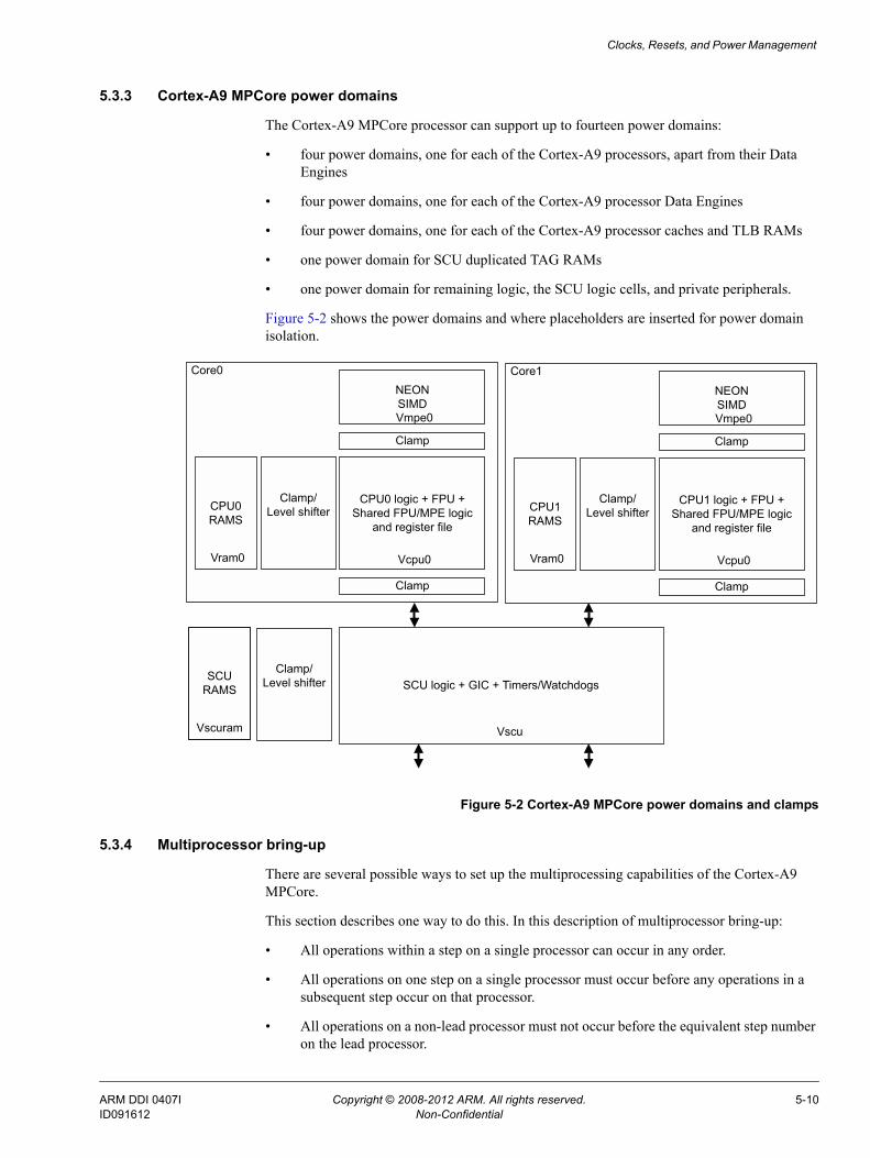
Clocks, Resets, and Power Management
5.3.3 Cortex-A9 MPCore power domains
The Cortex-A9 MPCore processor can support up to fourteen power domains:
• four power domains, one for each of the Cortex-A9 processors, apart from their Data Engines
• four power domains, one for each of the Cortex-A9 processor Data Engines
• four power domains, one for each of the Cortex-A9 processor caches and TLB RAMs
• one power domain for SCU duplicated TAG RAMs
• one power domain for remaining logic, the SCU logic cells, and private peripherals.
Figure 5-2 shows the power domains and where placeholders are inserted for power domain isolation.
Figure 5-2 Cortex-A9 MPCore power domains and clamps
5.3.4 Multiprocessor bring-up
There are several possible ways to set up the multiprocessing capabilities of the Cortex-A9 MPCore.
This section describes one way to do this. In this description of multiprocessor bring-up:
• All operations within a step on a single processor can occur in any order.
• All operations on one step on a single processor must occur before any operations in a subsequent step occur on that processor.
• All operations on a non-lead processor must not occur before the equivalent step number on the lead processor.
SCU logic + GIC + Timers/Watchdogs
Vscu
SCU RAMS
Vscuram
Core0
NEONSIMD
CPU0 logic + FPU + Shared FPU/MPE logic
and register file
Clamp
Vmpe0
Vcpu0
Clamp
CPU0 RAMS
Vram0
Clamp/Level shifter
Core1
NEONSIMD
CPU1 logic + FPU + Shared FPU/MPE logic
and register file
Clamp
Vmpe0
Vcpu0
Clamp
CPU1 RAMS
Vram0
Clamp/Level shifter
Clamp/Level shifter
ARM DDI 0407I Copyright © 2008-2012 ARM. All rights reserved. 5-10ID091612 Non-Confidential
Clocks, Resets, and Power Management
No other ordering applies.
For the primary processor:1. Invalidate:
• the SCU duplicate tags for all processors• the data cache.
2. Enable the SCU.3. Enable the data cache, set the SMP mode with ACTLR.SMP=1.
For non-primary processors:1. Invalidate the data cache.2. Wait for the SCU to be enabled by the primary processor.3. Enable the data cache, set the SMP mode with ACTLR.SMP=1.
Note L2C-310 cache controller setup is fully independent. You can perform setup at any time, before or after the Cortex-A9 MPCore multiprocessing bring-up.
ARM DDI 0407I Copyright © 2008-2012 ARM. All rights reserved. 5-11ID091612 Non-Confidential
Chapter 6 Debug
This chapter describes some of the debug and trace considerations in Cortex-A9 MPCore designs. It contains the following sections:• External Debug Interface Signals on page 6-2• Cortex-A9 MPCore APB Debug interface and memory map on page 6-3.
ARM DDI 0407I Copyright © 2008-2012 ARM. All rights reserved. 6-1ID091612 Non-Confidential
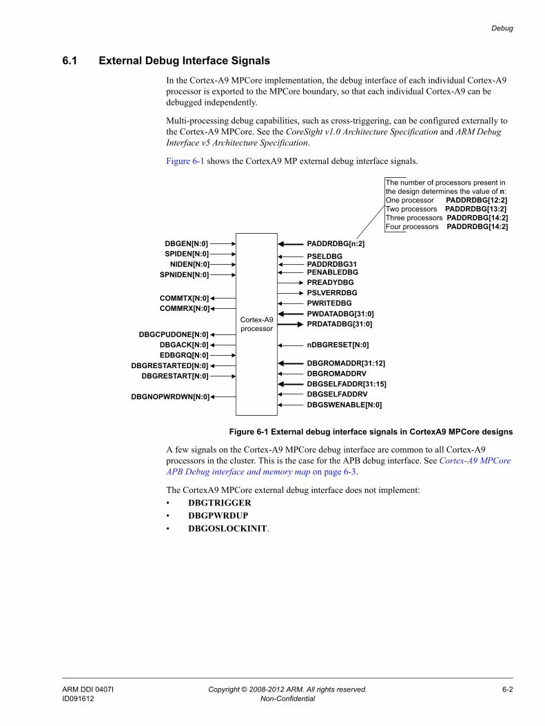
Debug
6.1 External Debug Interface SignalsIn the Cortex-A9 MPCore implementation, the debug interface of each individual Cortex-A9 processor is exported to the MPCore boundary, so that each individual Cortex-A9 can be debugged independently.
Multi-processing debug capabilities, such as cross-triggering, can be configured externally to the Cortex-A9 MPCore. See the CoreSight v1.0 Architecture Specification and ARM Debug Interface v5 Architecture Specification.
Figure 6-1 shows the CortexA9 MP external debug interface signals.
Figure 6-1 External debug interface signals in CortexA9 MPCore designs
A few signals on the Cortex-A9 MPCore debug interface are common to all Cortex-A9 processors in the cluster. This is the case for the APB debug interface. See Cortex-A9 MPCore APB Debug interface and memory map on page 6-3.
The CortexA9 MPCore external debug interface does not implement:• DBGTRIGGER• DBGPWRDUP• DBGOSLOCKINIT.
Cortex-A9processor
SPIDEN[N:0]
SPNIDEN[N:0]
DBGEN[N:0]
NIDEN[N:0]
COMMTX[N:0]COMMRX[N:0]
DBGCPUDONE[N:0]
DBGRESTARTED[N:0]
DBGNOPWRDWN[N:0]
DBGACK[N:0]EDBGRQ[N:0]
DBGRESTART[N:0]
PSELDBG
PADDRDBG[n:2]
PRDATADBG[31:0]
PENABLEDBGPREADYDBGPSLVERRDBGPWRITEDBG
DBGROMADDR[31:12]DBGROMADDRVDBGSELFADDR[31:15]DBGSELFADDRVDBGSWENABLE[N:0]
PWDATADBG[31:0]
nDBGRESET[N:0]
PADDRDBG31
The number of processors present in the design determines the value of n:One processor PADDRDBG[12:2]Two processors PADDRDBG[13:2]Three processors PADDRDBG[14:2]Four processors PADDRDBG[14:2]
ARM DDI 0407I Copyright © 2008-2012 ARM. All rights reserved. 6-2ID091612 Non-Confidential
Debug
6.2 Cortex-A9 MPCore APB Debug interface and memory mapEach Cortex-A9 processor contains two 4KB CoreSight components, for the debug and performance monitor resources, mapped in a contiguous 8KB memory region.See the Cortex-A9 TRM for detailed memory mapping of this 8KB memory region.
The Cortex-A9 MPCore has a single Debug APB interface to access the individual Cortex-A9 processors in the cluster.Because it contains between one and four individual Cortex-A9 processors, the Cortex-A9 MPCore appears as an 8KB, 16KB, 24KB, or 32KB CoreSight memory region, accessed when PSELDBG is asserted. The following sections describe the uses of PADDRDBG in the following Cortex-A9 MPCore configurations:• A single Cortex-A9 processor configuration• Two Cortex-A9 processors configuration• Three Cortex-A9 processors configuration• Four Cortex-A9 processors configuration on page 6-4.
6.2.1 A single Cortex-A9 processor configuration
In this configuration, PADDRDBG is [12:0].
PADDRDBG[12] is used to select the debug or performance monitor area of the processor:
• Use PADDRDBG[12] = 0 to access the debug area of the Cortex-A9 processor
• Use PADDRDBG[12] = 1 to access the performance monitor area of the Cortex-A9 processor.
6.2.2 Two Cortex-A9 processors configuration
In this configuration, PADDRDBG is [13:0].
PADDRDBG[13] is used to select which of the processors is accessed:• Use PADDRDBG[13] = 0 to access CPU0 resources• Use PADDRDBG[13] = 1 to access CPU1 resources.
PADDRDBG[12] is used to select the debug or performance monitor area of the processor:
• Use PADDRDBG[12] = 0 to access the debug area of the selected Cortex-A9 processor
• Use PADDRDBG[12] = 1 to access the performance monitor area of the selected Cortex-A9 processor
6.2.3 Three Cortex-A9 processors configuration
In this configuration, PADDRDBG is [14:0]
PADDRDBG[14:13] is used to select which of the processors is accessed:• Use PADDRDBG[14:13] = 00 to access CPU0 resources• Use PADDRDBG[14:13] = 01 to access CPU1 resources• Use PADDRDBG[14:13] = 10 to access CPU2 resources.
PADDRDBG[12] is used to select the debug or performance monitor area of the processor
• Use PADDRDBG[12] = 0 to access the debug area of the selected Cortex-A9 processor.
• Use PADDRDBG[12] = 1 to access the performance monitor area of the selected Cortex-A9 processor.
ARM DDI 0407I Copyright © 2008-2012 ARM. All rights reserved. 6-3ID091612 Non-Confidential
Debug
Note In this configuration, the external CoreSight system must ensure that the Cortex-A9 MPCore is never accessed with PADDRDBG[14:13] = 11. When PADDRDBG[14:13] = 11, PSELDBG must not be asserted.
6.2.4 Four Cortex-A9 processors configuration
In this configuration, PADDRDBG is [14:0]
PADDRDBG[14:13] is used to select which of the processors is accessed:• Use PADDRDBG[14:13] = 00 to access CPU0 resources• Use PADDRDBG[14:13] = 01 to access CPU1 resources• Use PADDRDBG[14:13] = 10 to access CPU2 resources• Use PADDRDBG[14:13] = 11 to access CPU3 resources.
PADDRDBG[12] is used to select the debug or performance monitor area of the processor
• Use PADDRDBG[12] = 0 to access the debug area of the selected Cortex-A9 processor.
• Use PADDRDBG[12] = 1 to access the performance monitor area of the selected Cortex-A9 processor.
ARM DDI 0407I Copyright © 2008-2012 ARM. All rights reserved. 6-4ID091612 Non-Confidential
Appendix A Signal Descriptions
This appendix describes the Cortex-A9 MPCore signals. In signal names such as TEINIT[N:0], the value of N is one less than the number of processors in your design The appendix contains the following sections:• Clock and clock control signals on page A-2• Resets and reset control signals on page A-3• Interrupts on page A-4• Configuration signals on page A-5• WFE and WFI Standby signals on page A-7• Power management signals on page A-8• AXI interfaces on page A-10• Performance monitoring signals on page A-18• Exception flags signals on page A-19• Parity error signals on page A-20• MBIST interface on page A-21• Scan test signal on page A-22• External Debug interface on page A-23• PTM interface signals on page A-27.
ARM DDI 0407I Copyright © 2008-2012 ARM. All rights reserved. A-1ID091612 Non-Confidential
Signal Descriptions
A.1 Clock and clock control signalsTable A-1 shows the clock and clock control signals.
See Chapter 5 Clocks, Resets, and Power Management.
Table A-1 Cortex-A9 MPCore clocks and clock control signals
Name I/O Source Description
CLK I Clock controller Global clock
MAXCLKLATENCY[2:0] I Implementation-specific static value Control dynamic clock gating delays.These pins are sampled during reset of the processor.
PERIPHCLK I Clock controller Clock for the timer and Interrupt Controller
PERIPHCLKEN I Clock controller Clock enable for the timer and Interrupt Controller
ARM DDI 0407I Copyright © 2008-2012 ARM. All rights reserved. A-2ID091612 Non-Confidential
Signal Descriptions
A.2 Resets and reset control signalsTable A-2 shows the reset signals.
Table A-3 shows the clock control signals that are used to cut the clocks during reset sequences. NEONCLCKOFF[N:0] is only present when there is a Data Engine in your design. See Chapter 5 Clocks, Resets, and Power Management.
Table A-4 shows the watchdog request reset signal.
See Chapter 4 Global timer, private timers, and watchdog registers.
Table A-2 Reset signals
Name I/O Source Description
nCPURESET[N:0] I Reset controller or clock controller Individual Cortex-A9 processor resets
nDBGRESET[N:0] I Processor debug logic resets
nNEONRESET[N:0]a I Cortex-A9 MPE SIMD logic resets
nPERIPHRESET I Timer and interrupt controller reset
nSCURESET I SCU global reset
nWDRESET[N:0] I Processor watchdog resets
a. Only if an MPE is present
Table A-3 Reset clock control signals
Name I/O Source Description
CPUCLKOFF[N:0] I Reset controller Individual Cortex-A9 Processor CPU clock enable, active-LOW:0 Clock is enabled. 1 Clock is stopped.
NEONCLKOFF[N:0] I MPE SIMD logic clock control:0 Do not cut MPE SIMD logic clock.1 Cut MPE SIMD logic clock.
Table A-4 Watchdog request reset signal
Name I/O Destination Description
WDRESETREQ[N:0] O System exception controller Processor watchdog reset requests
ARM DDI 0407I Copyright © 2008-2012 ARM. All rights reserved. A-3ID091612 Non-Confidential
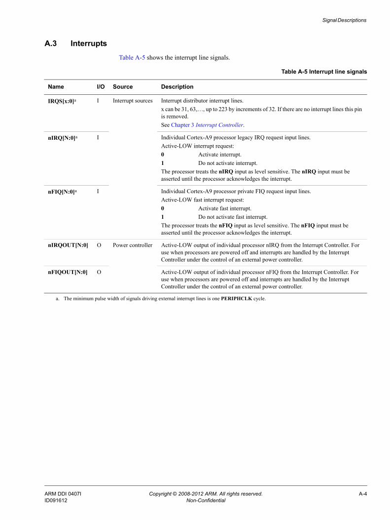
Signal Descriptions
A.3 InterruptsTable A-5 shows the interrupt line signals.
Table A-5 Interrupt line signals
Name I/O Source Description
IRQS[x:0]a I Interrupt sources Interrupt distributor interrupt lines.x can be 31, 63,…, up to 223 by increments of 32. If there are no interrupt lines this pin is removed.See Chapter 3 Interrupt Controller.
nIRQ[N:0]a I Individual Cortex-A9 processor legacy IRQ request input lines.Active-LOW interrupt request:0 Activate interrupt.1 Do not activate interrupt.The processor treats the nIRQ input as level sensitive. The nIRQ input must be asserted until the processor acknowledges the interrupt.
nFIQ[N:0]a I Individual Cortex-A9 processor private FIQ request input lines.Active-LOW fast interrupt request:0 Activate fast interrupt.1 Do not activate fast interrupt.The processor treats the nFIQ input as level sensitive. The nFIQ input must be asserted until the processor acknowledges the interrupt.
nIRQOUT[N:0] O Power controller Active-LOW output of individual processor nIRQ from the Interrupt Controller. For use when processors are powered off and interrupts are handled by the Interrupt Controller under the control of an external power controller.
nFIQOUT[N:0] O Active-LOW output of individual processor nFIQ from the Interrupt Controller. For use when processors are powered off and interrupts are handled by the Interrupt Controller under the control of an external power controller.
a. The minimum pulse width of signals driving external interrupt lines is one PERIPHCLK cycle.
ARM DDI 0407I Copyright © 2008-2012 ARM. All rights reserved. A-4ID091612 Non-Confidential
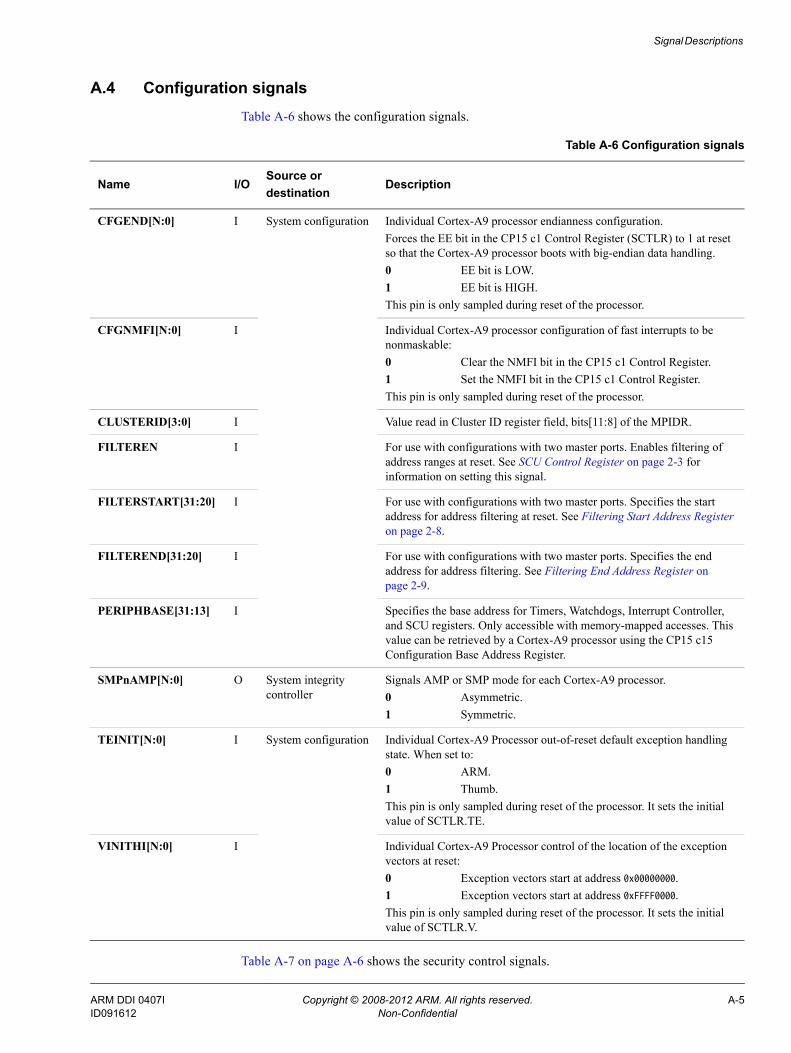
Signal Descriptions
A.4 Configuration signalsTable A-6 shows the configuration signals.
Table A-7 on page A-6 shows the security control signals.
Table A-6 Configuration signals
Name I/OSource ordestination
Description
CFGEND[N:0] I System configuration Individual Cortex-A9 processor endianness configuration. Forces the EE bit in the CP15 c1 Control Register (SCTLR) to 1 at reset so that the Cortex-A9 processor boots with big-endian data handling.0 EE bit is LOW.1 EE bit is HIGH. This pin is only sampled during reset of the processor.
CFGNMFI[N:0] I Individual Cortex-A9 processor configuration of fast interrupts to be nonmaskable:0 Clear the NMFI bit in the CP15 c1 Control Register.1 Set the NMFI bit in the CP15 c1 Control Register.This pin is only sampled during reset of the processor.
CLUSTERID[3:0] I Value read in Cluster ID register field, bits[11:8] of the MPIDR.
FILTEREN I For use with configurations with two master ports. Enables filtering of address ranges at reset. See SCU Control Register on page 2-3 for information on setting this signal.
FILTERSTART[31:20] I For use with configurations with two master ports. Specifies the start address for address filtering at reset. See Filtering Start Address Register on page 2-8.
FILTEREND[31:20] I For use with configurations with two master ports. Specifies the end address for address filtering. See Filtering End Address Register on page 2-9.
PERIPHBASE[31:13] I Specifies the base address for Timers, Watchdogs, Interrupt Controller, and SCU registers. Only accessible with memory-mapped accesses. This value can be retrieved by a Cortex-A9 processor using the CP15 c15 Configuration Base Address Register.
SMPnAMP[N:0] O System integrity controller
Signals AMP or SMP mode for each Cortex-A9 processor.0 Asymmetric.1 Symmetric.
TEINIT[N:0] I System configuration Individual Cortex-A9 Processor out-of-reset default exception handling state. When set to:0 ARM.1 Thumb.This pin is only sampled during reset of the processor. It sets the initial value of SCTLR.TE.
VINITHI[N:0] I Individual Cortex-A9 Processor control of the location of the exception vectors at reset:0 Exception vectors start at address 0x00000000.1 Exception vectors start at address 0xFFFF0000.This pin is only sampled during reset of the processor. It sets the initial value of SCTLR.V.
ARM DDI 0407I Copyright © 2008-2012 ARM. All rights reserved. A-5ID091612 Non-Confidential
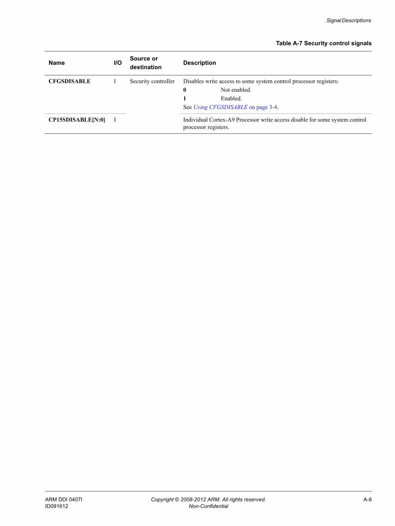
Signal Descriptions
Table A-7 Security control signals
Name I/OSource ordestination
Description
CFGSDISABLE I Security controller Disables write access to some system control processor registers:0 Not enabled.1 Enabled.See Using CFGSDISABLE on page 3-4.
CP15SDISABLE[N:0] I Individual Cortex-A9 Processor write access disable for some system control processor registers.
ARM DDI 0407I Copyright © 2008-2012 ARM. All rights reserved. A-6ID091612 Non-Confidential
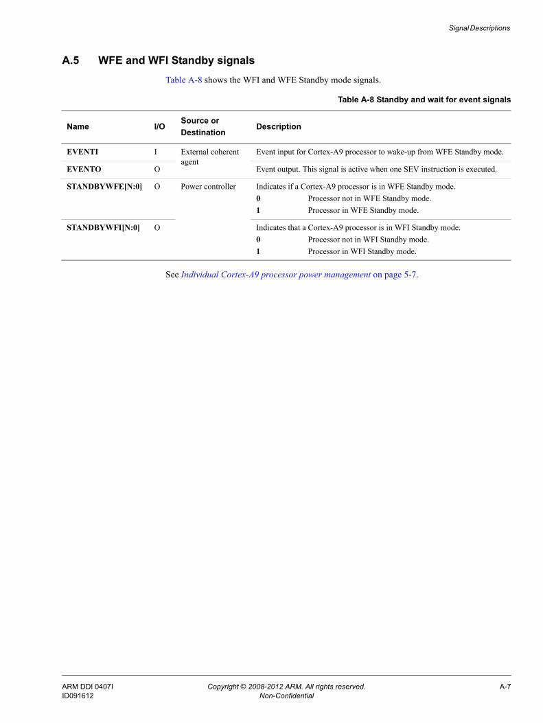
Signal Descriptions
A.5 WFE and WFI Standby signalsTable A-8 shows the WFI and WFE Standby mode signals.
See Individual Cortex-A9 processor power management on page 5-7.
Table A-8 Standby and wait for event signals
Name I/OSource orDestination
Description
EVENTI I External coherent agent
Event input for Cortex-A9 processor to wake-up from WFE Standby mode.
EVENTO O Event output. This signal is active when one SEV instruction is executed.
STANDBYWFE[N:0] O Power controller Indicates if a Cortex-A9 processor is in WFE Standby mode.0 Processor not in WFE Standby mode.1 Processor in WFE Standby mode.
STANDBYWFI[N:0] O Indicates that a Cortex-A9 processor is in WFI Standby mode.0 Processor not in WFI Standby mode.1 Processor in WFI Standby mode.
ARM DDI 0407I Copyright © 2008-2012 ARM. All rights reserved. A-7ID091612 Non-Confidential
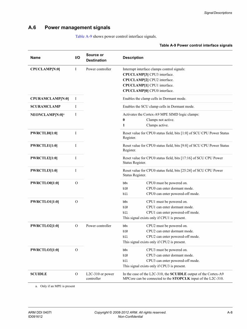
Signal Descriptions
A.6 Power management signalsTable A-9 shows power control interface signals.
Table A-9 Power control interface signals
Name I/OSource orDestination
Description
CPUCLAMP[N:0] I Power controller Interrupt interface clamps control signals:CPUCLAMP[3] CPU3 interface.CPUCLAMP[2] CPU2 interface.CPUCLAMP[1] CPU1 interface.CPUCLAMP[0] CPU0 interface.
CPURAMCLAMP[N:0] I Enables the clamp cells in Dormant mode.
SCURAMCLAMP I Enables the SCU clamp cells in Dormant mode.
NEONCLAMP[N:0]a I Activates the Cortex-A9 MPE SIMD logic clamps:0 Clamps not active.1 Clamps active.
PWRCTLI0[1:0] I Reset value for CPU0 status field, bits [1:0] of SCU CPU Power Status Register.
PWRCTLI1[1:0] I Reset value for CPU0 status field, bits [9:8] of SCU CPU Power Status Register.
PWRCTLI2[1:0] I Reset value for CPU0 status field, bits [17:16] of SCU CPU Power Status Register.
PWRCTLI3[1:0] I Reset value for CPU0 status field, bits [25:24] of SCU CPU Power Status Register.
PWRCTLO0[1:0] O b0x CPU0 must be powered on.b10 CPU0 can enter dormant mode.b11 CPU0 can enter powered-off mode.
PWRCTLO1[1:0] O b0x CPU1 must be powered on.b10 CPU1 can enter dormant mode.b11 CPU1 can enter powered-off mode.This signal exists only if CPU1 is present.
PWRCTLO2[1:0] O Power controller b0x CPU2 must be powered on.b10 CPU2 can enter dormant mode.b11 CPU2 can enter powered-off mode.This signal exists only if CPU2 is present.
PWRCTLO3[1:0] O b0x CPU3 must be powered on.b10 CPU3 can enter dormant mode.b11 CPU3 can enter powered-off mode.This signal exists only if CPU3 is present.
SCUIDLE O L2C-310 or power controller
In the case of the L2C-310, the SCUIDLE output of the Cortex-A9 MPCore can be connected to the STOPCLK input of the L2C-310.
a. Only if an MPE is present
ARM DDI 0407I Copyright © 2008-2012 ARM. All rights reserved. A-8ID091612 Non-Confidential

Signal Descriptions
See SCU CPU Power Status Register on page 2-6. See also Communication to the Power Management Controller on page 5-9.
ARM DDI 0407I Copyright © 2008-2012 ARM. All rights reserved. A-9ID091612 Non-Confidential
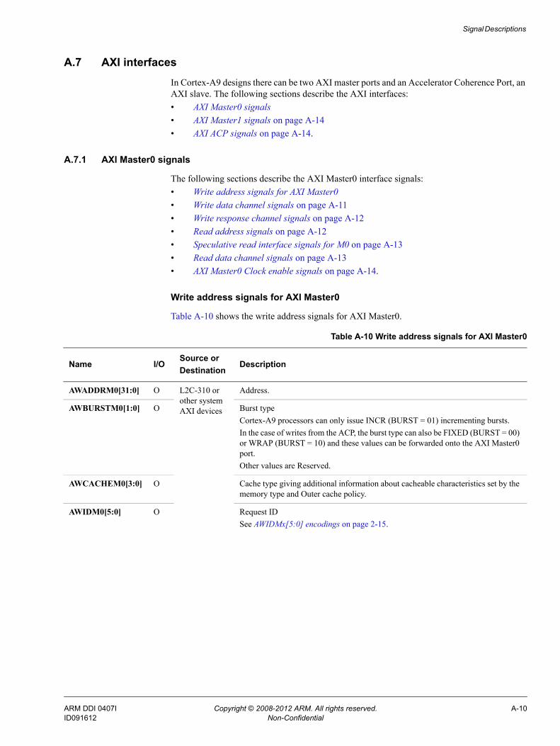
Signal Descriptions
A.7 AXI interfacesIn Cortex-A9 designs there can be two AXI master ports and an Accelerator Coherence Port, an AXI slave. The following sections describe the AXI interfaces:• AXI Master0 signals• AXI Master1 signals on page A-14• AXI ACP signals on page A-14.
A.7.1 AXI Master0 signals
The following sections describe the AXI Master0 interface signals:• Write address signals for AXI Master0• Write data channel signals on page A-11• Write response channel signals on page A-12• Read address signals on page A-12• Speculative read interface signals for M0 on page A-13• Read data channel signals on page A-13• AXI Master0 Clock enable signals on page A-14.
Write address signals for AXI Master0
Table A-10 shows the write address signals for AXI Master0.
Table A-10 Write address signals for AXI Master0
Name I/OSource orDestination
Description
AWADDRM0[31:0] O L2C-310 or other system AXI devices
Address.
AWBURSTM0[1:0] O Burst typeCortex-A9 processors can only issue INCR (BURST = 01) incrementing bursts.In the case of writes from the ACP, the burst type can also be FIXED (BURST = 00) or WRAP (BURST = 10) and these values can be forwarded onto the AXI Master0 port.Other values are Reserved.
AWCACHEM0[3:0] O Cache type giving additional information about cacheable characteristics set by the memory type and Outer cache policy.
AWIDM0[5:0] O Request IDSee AWIDMx[5:0] encodings on page 2-15.
ARM DDI 0407I Copyright © 2008-2012 ARM. All rights reserved. A-10ID091612 Non-Confidential
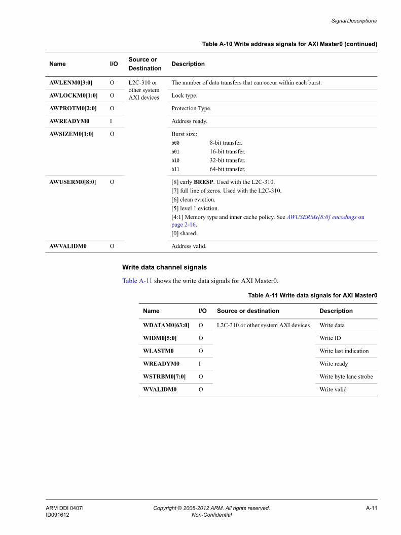
Signal Descriptions
Write data channel signals
Table A-11 shows the write data signals for AXI Master0.
AWLENM0[3:0] O L2C-310 or other system AXI devices
The number of data transfers that can occur within each burst.
AWLOCKM0[1:0] O Lock type.
AWPROTM0[2:0] O Protection Type.
AWREADYM0 I Address ready.
AWSIZEM0[1:0] O Burst size:b00 8-bit transfer.b01 16-bit transfer.b10 32-bit transfer.b11 64-bit transfer.
AWUSERM0[8:0] O [8] early BRESP. Used with the L2C-310.[7] full line of zeros. Used with the L2C-310.[6] clean eviction.[5] level 1 eviction.[4:1] Memory type and inner cache policy. See AWUSERMx[8:0] encodings on page 2-16.[0] shared.
AWVALIDM0 O Address valid.
Table A-10 Write address signals for AXI Master0 (continued)
Name I/OSource orDestination
Description
Table A-11 Write data signals for AXI Master0
Name I/O Source or destination Description
WDATAM0[63:0] O L2C-310 or other system AXI devices Write data
WIDM0[5:0] O Write ID
WLASTM0 O Write last indication
WREADYM0 I Write ready
WSTRBM0[7:0] O Write byte lane strobe
WVALIDM0 O Write valid
ARM DDI 0407I Copyright © 2008-2012 ARM. All rights reserved. A-11ID091612 Non-Confidential
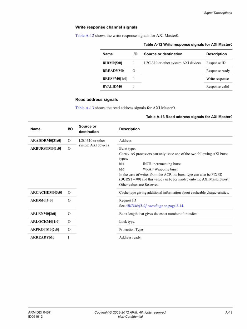
Signal Descriptions
Write response channel signals
Table A-12 shows the write response signals for AXI Master0.
Read address signals
Table A-13 shows the read address signals for AXI Master0.
Table A-12 Write response signals for AXI Master0
Name I/O Source or destination Description
BIDM0[5:0] I L2C-310 or other system AXI devices Response ID
BREADYM0 O Response ready
BRESPM0[1:0] I Write response
BVALIDM0 I Response valid
Table A-13 Read address signals for AXI Master0
Name I/OSource ordestination
Description
ARADDRM0[31:0] O L2C-310 or other system AXI devices
Address
ARBURSTM0[1:0] O Burst type:Cortex-A9 processors can only issue one of the two following AXI burst types:b01 INCR incrementing burstb10 WRAP Wrapping burst.In the case of writes from the ACP, the burst type can also be FIXED (BURST = 00) and this value can be forwarded onto the AXI Master0 port. Other values are Reserved.
ARCACHEM0[3:0] O Cache type giving additional information about cacheable characteristics.
ARIDM0[5:0] O Request IDSee ARIDMx[5:0] encodings on page 2-14.
ARLENM0[3:0] O Burst length that gives the exact number of transfers.
ARLOCKM0[1:0] O Lock type.
ARPROTM0[2:0] O Protection Type
ARREADYM0 I Address ready.
ARM DDI 0407I Copyright © 2008-2012 ARM. All rights reserved. A-12ID091612 Non-Confidential
Signal Descriptions
Speculative read interface signals for M0
Table A-14 shows the interface signals on M0 for speculative read accesses between Cortex-A9MPCore and L2C-310.
Read data channel signals
Table A-15 shows the read data signals for AXI Master0.
ARSIZEM0[1:0] O L2C-310 or other system AXI devices
Burst size:b00 8-bit transfer.b01 16-bit transfer.b10 32-bit transfer.b11 64-bit transfer.
ARUSERM0[6:0] O Sideband information:[6] Speculative linefill, used with L2C-310[5] prefetch hint, used with L2C-310[4:1] inner attributes:b0000 Strongly-ordered.b0001 Device.b0011 Normal Memory Non-Cacheable.b0110 Write-Through.b0111 Write-Back no Write Allocate.b1111 Write-Back Write Allocate. [0] shared bit.See ARUSERMx[6:0] encodings on page 2-15.
ARVALIDM0 O Address valid.
Table A-13 Read address signals for AXI Master0 (continued)
Name I/OSource ordestination
Description
Table A-14 L2C-310 signals on M0
Name I/O Source Description
SRENDM0[3:0] I L2C-310 Speculative linefill confirmations from L2C-310.
SRIDM0[23:0] I Speculative confirmed IDs from L2C-310
Table A-15 Read data signals for AXI Master0
Name I/O Source or destination Description
RVALIDM0 I L2C-310 or other system AXI devices Read valid
RDATAM0[63:0] I Read data
RRESPM0[1:0] I Read response
RLASTM0 I Read Last indication
RIDM0[5:0] I Read ID
RREADYM0 O Read ready
ARM DDI 0407I Copyright © 2008-2012 ARM. All rights reserved. A-13ID091612 Non-Confidential
Signal Descriptions
AXI Master0 Clock enable signals
Table A-16 shows the AXI Master0 clock enable signals.
A.7.2 AXI Master1 signals
In designs that implement the AXI Master1 interface, the AXI Master1 interface signals are identical to the AXI Master0 interface signals, except that AXI Master1 signals end in M1.This applies to all M0 AXI signals in addition to the Speculative Read Interface signals SREND and SRID.
A.7.3 AXI ACP signals
The following sections describe the AXI ACP interface signals:• Write address signals for AXI ACP on page A-15• Write data channel signals on page A-16• Write response channel signals on page A-16• Read address channel signals on page A-16• Read data channel signals on page A-17• Clock enable slave signal on page A-17.
Table A-16 AXI Master0 clock enable signals
Name I/O Source Description
INCLKENM0 I Clockcontroller
Clock enable for the AXI bus that enables the AXI interface to operate at either:• integer ratios of the system clock• half integer ratios of the system clock.See Interfaces on page 1-9.
OUTCLKENM0 I Clock enable for the AXI bus that enables the AXI interface to operate at either:• integer ratios of the system clock• half integer ratios of the system clock.See Interfaces on page 1-9.
ARM DDI 0407I Copyright © 2008-2012 ARM. All rights reserved. A-14ID091612 Non-Confidential
Signal Descriptions
Write address signals for AXI ACP
Table A-17 shows the AXI write address signals for AXI ACP.
Table A-17 Write address signals for AXI ACP
Name I/O Source or destination Description
AWADDRS[31:0] I External AXI master Address.
AWBURSTS[1:0] I Burst type.
AWCACHES[3:0] I Cache type giving additional information about cacheable characteristics.
AWIDS[2:0] I Request ID
AWLENS[3:0] I The number of data transfers that can occur within each burst.
AWLOCKS[0] I Lock type:0 Normal access.1 Exclusive access.Bit [1] is unused. Tie off LOW.
AWPROTS[2:0] I Protection Type.
AWREADYS O Address ready.
AWSIZES[1:0] I External AXI master Burst size:b00 8-bit transfer.b01 16-bit transfer.b10 32-bit transfer.b11 64-bit transfer.
AWUSERS[4:0] I Sideband information:[4:1] inner attributes:b0000 Strongly-ordered.b0001 Device.b0011 Normal Memory Non-Cacheable.b0110 Write-Through.b0111 Write-Back no Write Allocate.b1111 Write-Back Write Allocate. [0] shared.See AXI USER attributes encodings on page 2-15.
AWVALIDS I Address valid.
ARM DDI 0407I Copyright © 2008-2012 ARM. All rights reserved. A-15ID091612 Non-Confidential
Signal Descriptions
Write data channel signals
Table A-18 shows the AXI write data signals for AXI ACP.
Write response channel signals
Table A-19 shows the AXI write response signals for AXI ACP.
Read address channel signals
Table A-20 shows the AXI read address signals for AXI ACP.
Table A-18 Write data signals for AXI ACP
Name I/O Source or destination Description
WDATAS[63:0] I External AXI master Write data
WIDS[2:0] I Write ID
WLASTS I Write last indication
WREADYS O Write ready
WSTRBS[7:0] I Write byte lane strobe
WVALIDS I Write valid
Table A-19 Write response signals for AXI ACP
Name I/O Source or destination Description
BIDS[2:0] O External AXI master Response ID
BREADYS I Response ready
BRESPS[1:0] O Write response
BVALIDS O Response valid
Table A-20 Read address signals for AXI ACP
Name I/OSource ordestination
Description
ARADDRS[31:0] I External AXI master Address.
ARBURSTS[1:0] I Burst type.
ARCACHES[3:0] I Cache type giving additional information about cacheable characteristics.
ARIDS[2:0] I Request ID
ARLENS[3:0] I The number of data transfers that can occur within each burst.
ARM DDI 0407I Copyright © 2008-2012 ARM. All rights reserved. A-16ID091612 Non-Confidential
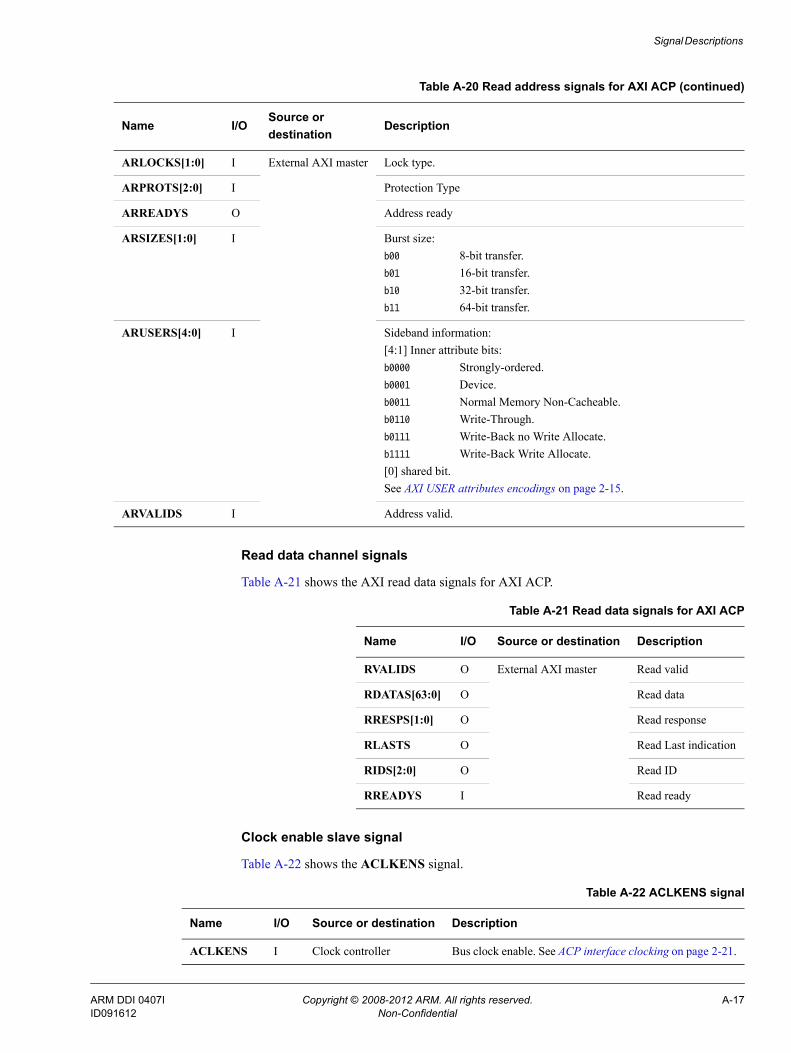
Signal Descriptions
Read data channel signals
Table A-21 shows the AXI read data signals for AXI ACP.
Clock enable slave signal
Table A-22 shows the ACLKENS signal.
ARLOCKS[1:0] I External AXI master Lock type.
ARPROTS[2:0] I Protection Type
ARREADYS O Address ready
ARSIZES[1:0] I Burst size:b00 8-bit transfer.b01 16-bit transfer.b10 32-bit transfer.b11 64-bit transfer.
ARUSERS[4:0] I Sideband information:[4:1] Inner attribute bits:b0000 Strongly-ordered.b0001 Device.b0011 Normal Memory Non-Cacheable.b0110 Write-Through.b0111 Write-Back no Write Allocate.b1111 Write-Back Write Allocate. [0] shared bit.See AXI USER attributes encodings on page 2-15.
ARVALIDS I Address valid.
Table A-20 Read address signals for AXI ACP (continued)
Name I/OSource ordestination
Description
Table A-21 Read data signals for AXI ACP
Name I/O Source or destination Description
RVALIDS O External AXI master Read valid
RDATAS[63:0] O Read data
RRESPS[1:0] O Read response
RLASTS O Read Last indication
RIDS[2:0] O Read ID
RREADYS I Read ready
Table A-22 ACLKENS signal
Name I/O Source or destination Description
ACLKENS I Clock controller Bus clock enable. See ACP interface clocking on page 2-21.
ARM DDI 0407I Copyright © 2008-2012 ARM. All rights reserved. A-17ID091612 Non-Confidential
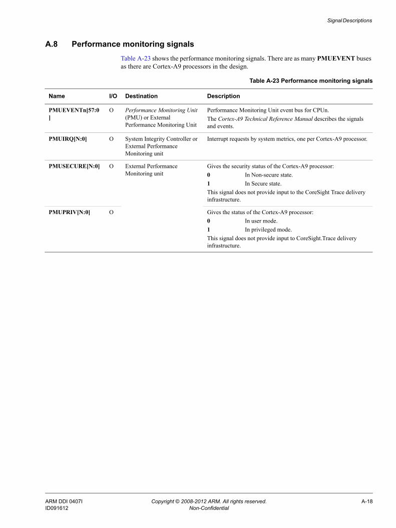
Signal Descriptions
A.8 Performance monitoring signalsTable A-23 shows the performance monitoring signals. There are as many PMUEVENT buses as there are Cortex-A9 processors in the design.
Table A-23 Performance monitoring signals
Name I/O Destination Description
PMUEVENTn[57:0]
O Performance Monitoring Unit (PMU) or External Performance Monitoring Unit
Performance Monitoring Unit event bus for CPUn.The Cortex-A9 Technical Reference Manual describes the signals and events.
PMUIRQ[N:0] O System Integrity Controller or External Performance Monitoring unit
Interrupt requests by system metrics, one per Cortex-A9 processor.
PMUSECURE[N:0] O External Performance Monitoring unit
Gives the security status of the Cortex-A9 processor:0 In Non-secure state. 1 In Secure state.This signal does not provide input to the CoreSight Trace delivery infrastructure.
PMUPRIV[N:0] O Gives the status of the Cortex-A9 processor:0 In user mode. 1 In privileged mode.This signal does not provide input to CoreSight.Trace delivery infrastructure.
ARM DDI 0407I Copyright © 2008-2012 ARM. All rights reserved. A-18ID091612 Non-Confidential
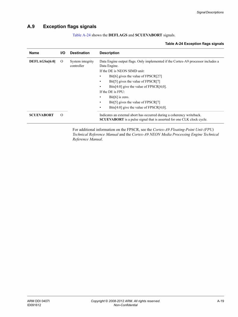
Signal Descriptions
A.9 Exception flags signalsTable A-24 shows the DEFLAGS and SCUEVABORT signals.
For additional information on the FPSCR, see the Cortex-A9 Floating-Point Unit (FPU) Technical Reference Manual and the Cortex-A9 NEON Media Processing Engine Technical Reference Manual.
Table A-24 Exception flags signals
Name I/O Destination Description
DEFLAGSn[6:0] O System integrity controller
Data Engine output flags. Only implemented if the Cortex-A9 processor includes a Data Engine.If the DE is NEON SIMD unit:• Bit[6] gives the value of FPSCR[27]• Bit[5] gives the value of FPSCR[7]• Bits[4:0] give the value of FPSCR[4;0].If the DE is FPU:• Bit[6] is zero.• Bit[5] gives the value of FPSCR[7]• Bits[4:0] give the value of FPSCR[4;0].
SCUEVABORT O Indicates an external abort has occurred during a coherency writeback. SCUEVABORT is a pulse signal that is asserted for one CLK clock cycle.
ARM DDI 0407I Copyright © 2008-2012 ARM. All rights reserved. A-19ID091612 Non-Confidential
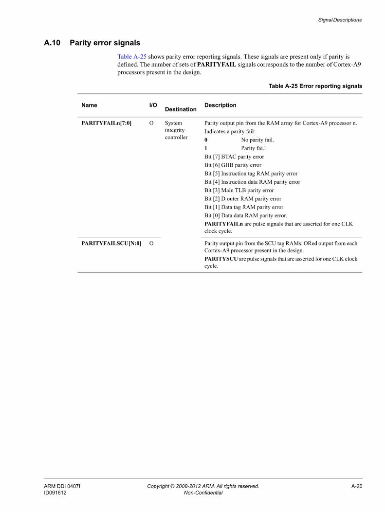
Signal Descriptions
A.10 Parity error signalsTable A-25 shows parity error reporting signals. These signals are present only if parity is defined. The number of sets of PARITYFAIL signals corresponds to the number of Cortex-A9 processors present in the design.
Table A-25 Error reporting signals
Name I/ODestination
Description
PARITYFAILn[7:0] O System integrity controller
Parity output pin from the RAM array for Cortex-A9 processor n. Indicates a parity fail:0 No parity fail.1 Parity fai.lBit [7] BTAC parity errorBit [6] GHB parity errorBit [5] Instruction tag RAM parity errorBit [4] Instruction data RAM parity errorBit [3] Main TLB parity errorBit [2] D outer RAM parity errorBit [1] Data tag RAM parity errorBit [0] Data data RAM parity error.PARITYFAILn are pulse signals that are asserted for one CLK clock cycle.
PARITYFAILSCU[N:0] O Parity output pin from the SCU tag RAMs. ORed output from each Cortex-A9 processor present in the design.PARITYSCU are pulse signals that are asserted for one CLK clock cycle.
ARM DDI 0407I Copyright © 2008-2012 ARM. All rights reserved. A-20ID091612 Non-Confidential
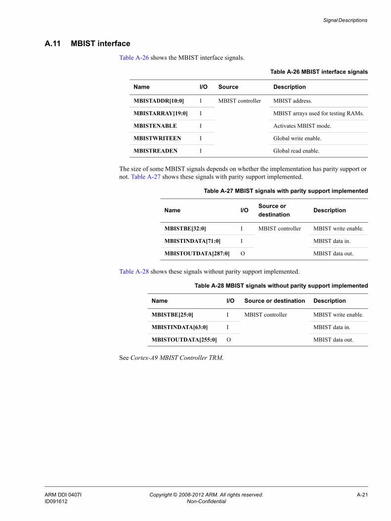
Signal Descriptions
A.11 MBIST interfaceTable A-26 shows the MBIST interface signals.
The size of some MBIST signals depends on whether the implementation has parity support or not. Table A-27 shows these signals with parity support implemented.
Table A-28 shows these signals without parity support implemented.
See Cortex-A9 MBIST Controller TRM.
Table A-26 MBIST interface signals
Name I/O Source Description
MBISTADDR[10:0] I MBIST controller MBIST address.
MBISTARRAY[19:0] I MBIST arrays used for testing RAMs.
MBISTENABLE I Activates MBIST mode.
MBISTWRITEEN I Global write enable.
MBISTREADEN I Global read enable.
Table A-27 MBIST signals with parity support implemented
Name I/OSource ordestination
Description
MBISTBE[32:0] I MBIST controller MBIST write enable.
MBISTINDATA[71:0] I MBIST data in.
MBISTOUTDATA[287:0] O MBIST data out.
Table A-28 MBIST signals without parity support implemented
Name I/O Source or destination Description
MBISTBE[25:0] I MBIST controller MBIST write enable.
MBISTINDATA[63:0] I MBIST data in.
MBISTOUTDATA[255:0] O MBIST data out.
ARM DDI 0407I Copyright © 2008-2012 ARM. All rights reserved. A-21ID091612 Non-Confidential
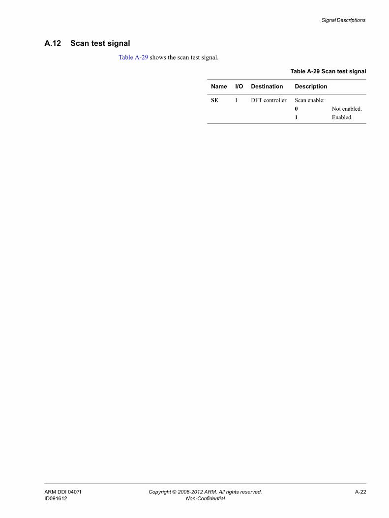
Signal Descriptions
A.12 Scan test signalTable A-29 shows the scan test signal.
Table A-29 Scan test signal
Name I/O Destination Description
SE I DFT controller Scan enable:0 Not enabled.1 Enabled.
ARM DDI 0407I Copyright © 2008-2012 ARM. All rights reserved. A-22ID091612 Non-Confidential
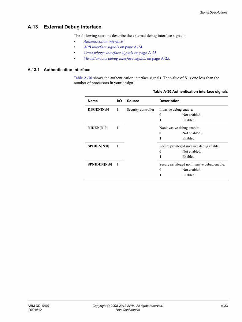
Signal Descriptions
A.13 External Debug interfaceThe following sections describe the external debug interface signals:• Authentication interface• APB interface signals on page A-24• Cross trigger interface signals on page A-25• Miscellaneous debug interface signals on page A-25.
A.13.1 Authentication interface
Table A-30 shows the authentication interface signals. The value of N is one less than the number of processors in your design.
Table A-30 Authentication interface signals
Name I/O Source Description
DBGEN[N:0] I Security controller Invasive debug enable:0 Not enabled.1 Enabled.
NIDEN[N:0] I Noninvasive debug enable:0 Not enabled.1 Enabled.
SPIDEN[N:0] I Secure privileged invasive debug enable:0 Not enabled.1 Enabled.
SPNIDEN[N:0] I Secure privileged noninvasive debug enable:0 Not enabled.1 Enabled.
ARM DDI 0407I Copyright © 2008-2012 ARM. All rights reserved. A-23ID091612 Non-Confidential
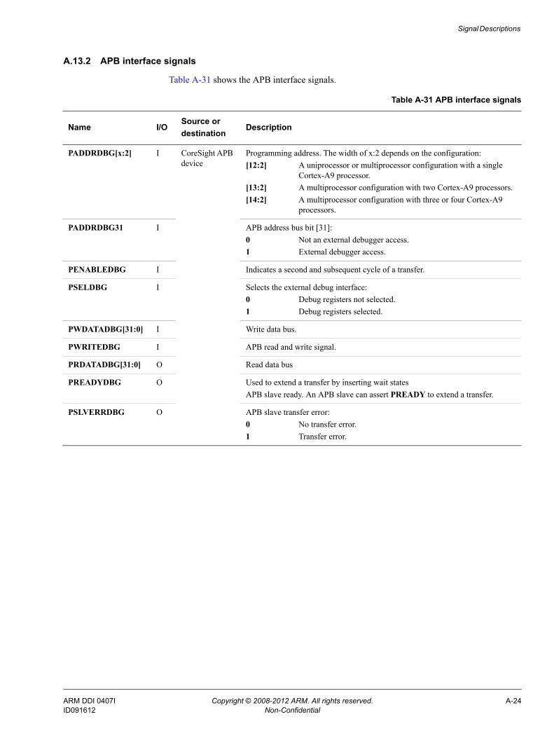
Signal Descriptions
A.13.2 APB interface signals
Table A-31 shows the APB interface signals.
Table A-31 APB interface signals
Name I/OSource ordestination
Description
PADDRDBG[x:2] I CoreSight APB device
Programming address. The width of x:2 depends on the configuration:[12:2] A uniprocessor or multiprocessor configuration with a single
Cortex-A9 processor.[13:2] A multiprocessor configuration with two Cortex-A9 processors.[14:2] A multiprocessor configuration with three or four Cortex-A9
processors.
PADDRDBG31 I APB address bus bit [31]: 0 Not an external debugger access.1 External debugger access.
PENABLEDBG I Indicates a second and subsequent cycle of a transfer.
PSELDBG I Selects the external debug interface:0 Debug registers not selected.1 Debug registers selected.
PWDATADBG[31:0] I Write data bus.
PWRITEDBG I APB read and write signal.
PRDATADBG[31:0] O Read data bus
PREADYDBG O Used to extend a transfer by inserting wait statesAPB slave ready. An APB slave can assert PREADY to extend a transfer.
PSLVERRDBG O APB slave transfer error:0 No transfer error.1 Transfer error.
ARM DDI 0407I Copyright © 2008-2012 ARM. All rights reserved. A-24ID091612 Non-Confidential
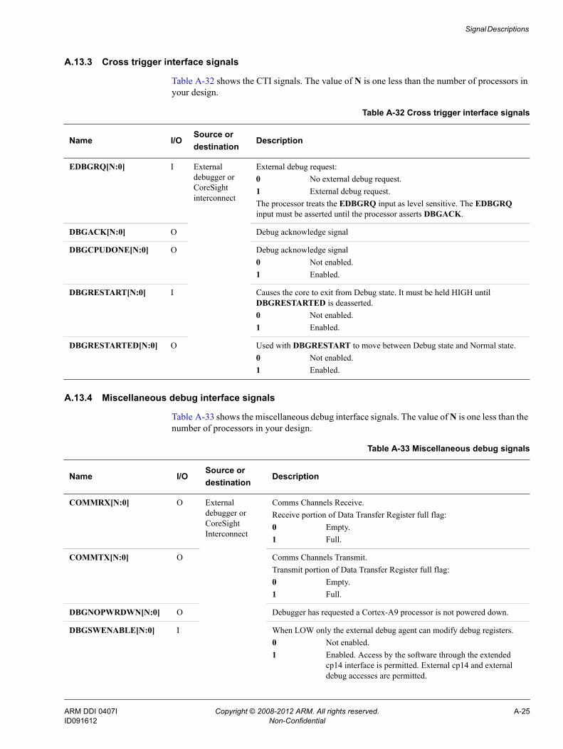
Signal Descriptions
A.13.3 Cross trigger interface signals
Table A-32 shows the CTI signals. The value of N is one less than the number of processors in your design.
A.13.4 Miscellaneous debug interface signals
Table A-33 shows the miscellaneous debug interface signals. The value of N is one less than the number of processors in your design.
Table A-32 Cross trigger interface signals
Name I/OSource ordestination
Description
EDBGRQ[N:0] I External debugger or CoreSight interconnect
External debug request:0 No external debug request.1 External debug request.The processor treats the EDBGRQ input as level sensitive. The EDBGRQ input must be asserted until the processor asserts DBGACK.
DBGACK[N:0] O Debug acknowledge signal
DBGCPUDONE[N:0] O Debug acknowledge signal0 Not enabled.1 Enabled.
DBGRESTART[N:0] I Causes the core to exit from Debug state. It must be held HIGH until DBGRESTARTED is deasserted.0 Not enabled.1 Enabled.
DBGRESTARTED[N:0] O Used with DBGRESTART to move between Debug state and Normal state.0 Not enabled.1 Enabled.
Table A-33 Miscellaneous debug signals
Name I/OSource ordestination
Description
COMMRX[N:0] O External debugger or CoreSight Interconnect
Comms Channels Receive.Receive portion of Data Transfer Register full flag:0 Empty.1 Full.
COMMTX[N:0] O Comms Channels Transmit.Transmit portion of Data Transfer Register full flag:0 Empty.1 Full.
DBGNOPWRDWN[N:0] O Debugger has requested a Cortex-A9 processor is not powered down.
DBGSWENABLE[N:0] I When LOW only the external debug agent can modify debug registers.0 Not enabled.1 Enabled. Access by the software through the extended
cp14 interface is permitted. External cp14 and external debug accesses are permitted.
ARM DDI 0407I Copyright © 2008-2012 ARM. All rights reserved. A-25ID091612 Non-Confidential
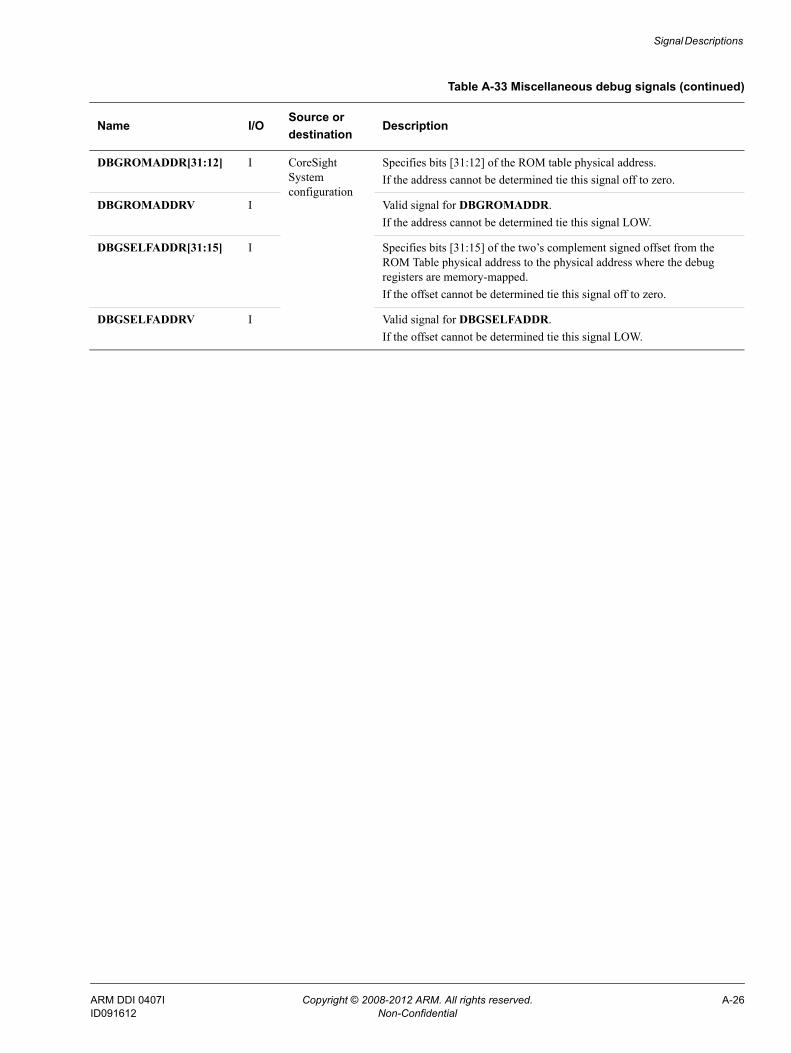
Signal Descriptions
DBGROMADDR[31:12] I CoreSight System configuration
Specifies bits [31:12] of the ROM table physical address.If the address cannot be determined tie this signal off to zero.
DBGROMADDRV I Valid signal for DBGROMADDR.If the address cannot be determined tie this signal LOW.
DBGSELFADDR[31:15] I Specifies bits [31:15] of the two’s complement signed offset from the ROM Table physical address to the physical address where the debug registers are memory-mapped.If the offset cannot be determined tie this signal off to zero.
DBGSELFADDRV I Valid signal for DBGSELFADDR.If the offset cannot be determined tie this signal LOW.
Table A-33 Miscellaneous debug signals (continued)
Name I/OSource ordestination
Description
ARM DDI 0407I Copyright © 2008-2012 ARM. All rights reserved. A-26ID091612 Non-Confidential
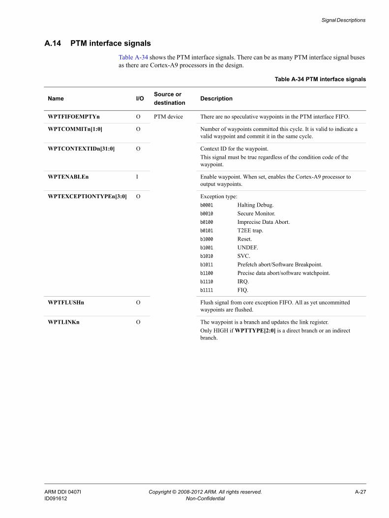
Signal Descriptions
A.14 PTM interface signalsTable A-34 shows the PTM interface signals. There can be as many PTM interface signal buses as there are Cortex-A9 processors in the design.
Table A-34 PTM interface signals
Name I/OSource ordestination
Description
WPTFIFOEMPTYn O PTM device There are no speculative waypoints in the PTM interface FIFO.
WPTCOMMITn[1:0] O Number of waypoints committed this cycle. It is valid to indicate a valid waypoint and commit it in the same cycle.
WPTCONTEXTIDn[31:0] O Context ID for the waypoint. This signal must be true regardless of the condition code of the waypoint.
WPTENABLEn I Enable waypoint. When set, enables the Cortex-A9 processor to output waypoints.
WPTEXCEPTIONTYPEn[3:0] O Exception type:b0001 Halting Debug.b0010 Secure Monitor.b0100 Imprecise Data Abort.b0101 T2EE trap.b1000 Reset.b1001 UNDEF.b1010 SVC.b1011 Prefetch abort/Software Breakpoint.b1100 Precise data abort/software watchpoint.b1110 IRQ.b1111 FIQ.
WPTFLUSHn O Flush signal from core exception FIFO. All as yet uncommitted waypoints are flushed.
WPTLINKn O The waypoint is a branch and updates the link register.Only HIGH if WPTTYPE[2:0] is a direct branch or an indirect branch.
ARM DDI 0407I Copyright © 2008-2012 ARM. All rights reserved. A-27ID091612 Non-Confidential
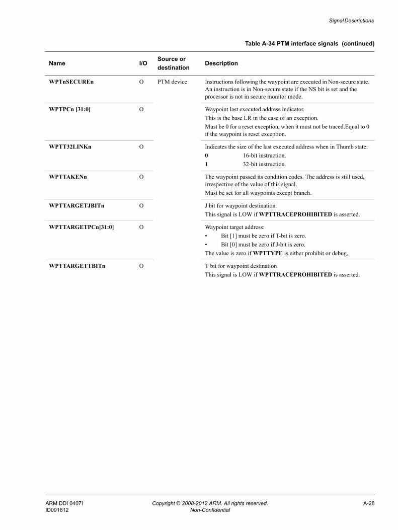
Signal Descriptions
WPTnSECUREn O PTM device Instructions following the waypoint are executed in Non-secure state. An instruction is in Non-secure state if the NS bit is set and the processor is not in secure monitor mode.
WPTPCn [31:0] O Waypoint last executed address indicator. This is the base LR in the case of an exception.Must be 0 for a reset exception, when it must not be traced.Equal to 0 if the waypoint is reset exception.
WPTT32LINKn O Indicates the size of the last executed address when in Thumb state:0 16-bit instruction.1 32-bit instruction.
WPTTAKENn O The waypoint passed its condition codes. The address is still used, irrespective of the value of this signal.Must be set for all waypoints except branch.
WPTTARGETJBITn O J bit for waypoint destination. This signal is LOW if WPTTRACEPROHIBITED is asserted.
WPTTARGETPCn[31:0] O Waypoint target address:• Bit [1] must be zero if T-bit is zero.• Bit [0] must be zero if J-bit is zero.The value is zero if WPTTYPE is either prohibit or debug.
WPTTARGETTBITn O T bit for waypoint destinationThis signal is LOW if WPTTRACEPROHIBITED is asserted.
Table A-34 PTM interface signals (continued)
Name I/OSource ordestination
Description
ARM DDI 0407I Copyright © 2008-2012 ARM. All rights reserved. A-28ID091612 Non-Confidential
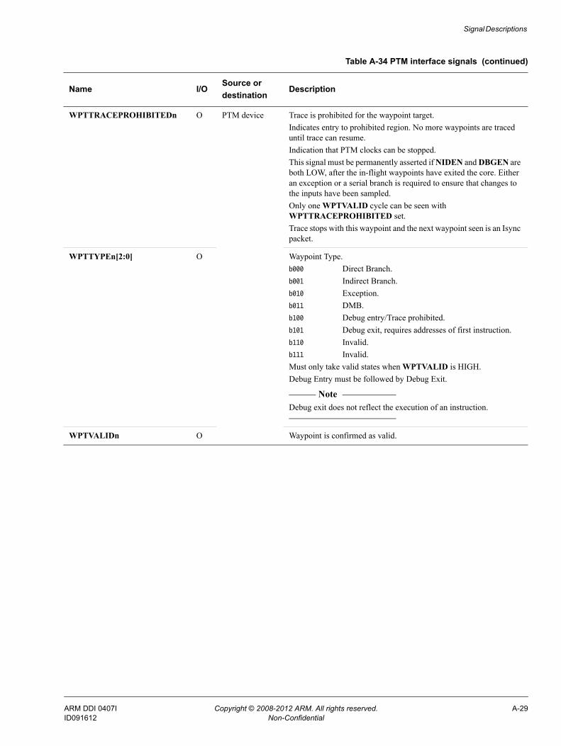
Signal Descriptions
WPTTRACEPROHIBITEDn O PTM device Trace is prohibited for the waypoint target.Indicates entry to prohibited region. No more waypoints are traced until trace can resume.Indication that PTM clocks can be stopped.This signal must be permanently asserted if NIDEN and DBGEN are both LOW, after the in-flight waypoints have exited the core. Either an exception or a serial branch is required to ensure that changes to the inputs have been sampled.Only one WPTVALID cycle can be seen with WPTTRACEPROHIBITED set.Trace stops with this waypoint and the next waypoint seen is an Isync packet.
WPTTYPEn[2:0] O Waypoint Type.b000 Direct Branch.b001 Indirect Branch.b010 Exception.b011 DMB.b100 Debug entry/Trace prohibited.b101 Debug exit, requires addresses of first instruction.b110 Invalid.b111 Invalid.Must only take valid states when WPTVALID is HIGH.Debug Entry must be followed by Debug Exit.
Note Debug exit does not reflect the execution of an instruction.
WPTVALIDn O Waypoint is confirmed as valid.
Table A-34 PTM interface signals (continued)
Name I/OSource ordestination
Description
ARM DDI 0407I Copyright © 2008-2012 ARM. All rights reserved. A-29ID091612 Non-Confidential
Appendix B Revisions
This appendix describes the technical changes between released issues of this books.
Table B-1 Issue A
Change Location
First release -
Table B-2 Differences between issue A and issue B
Change Location
Clarify the relationship between the GIC (PL390) and the Cortex-A9 Interrupt Controller
Chapter 3 Interrupt Controller.
Parity error option added Table 1-1 on page 1-5.
Clarify the role of the SCU with reference to data coherency and the non-support of instruction cache coherency
About the SCU on page 2-2.
Added information about exclusive accesses and address filtering Address filtering on page 2-2.
SSAC description corrected SCU Non-secure Access Control Register on page 2-11.
SSAC bit assignments corrected Table 2-9 on page 2-11.
Change STI, Software Triggered Interrupt, to SGI, Software Generated Interrupt
Throughout Chapter 3 Interrupt Controller.
INTID descriptions extended and clarified Throughout Chapter 3 Interrupt Controller.
ARM DDI 0407I Copyright © 2008-2012 ARM. All rights reserved. B-1ID091612 Non-Confidential
Revisions
Differences between issue B and issue C
Reset information added Timer and watchdog registers on page 5-3.
AXI transaction IDs section extended AXI transaction IDs on page 6-3.
AXI USER encodings section added AXI USER encodings on page 6-5.
EVENTI information extended and EVENTO information added WFE/SEV synchronization on page 6-9.
CLUSTERID[3:0] description corrected Configuration signals on page A-5.
DBGEN[3:0] description added Table A-30 on page A-23.
Table B-2 Differences between issue A and issue B (continued)
Change Location
Table B-3 Differences between issue B and issue C
Change Location
Design changes listed Product revisions on page 1-13.
New entries in the Private Memory map Table 2-2 on page 2-3.
Timers and watchdogs renamed Private timers and watchdogs Table 2-2 on page 2-3.
TLB size added as a configurable option Table 1-1 on page 1-5.
Timing diagrams added Figure 1-4 on page 1-25, Figure 1-5 on page 1-25, Figure 1-6 on page 1-26, and Figure 1-7 on page 1-26.
CPUCLKOFF and DECLKOFF added to Power-on reset Cortex-A9 MPCore reset on page 1-28. Configuration signals on page A-5.
Correction to Tag RAM sizes values Table 2-3 on page 2-5
Change in SCU Power Status Register layout SCU CPU Power Status Register on page 2-7
Additional PPI. There are five PPIs per Cortex-A9 processor interface
Interrupt types and sources on page 3-2.
PPI(4) added to the PPI Status Register PPI Status Register on page 3-10.
INT renamed IRQS SPI Status Registers on page 3-11. Interrupts on page A-4.
Chapter 5 renamed. It was “Private timers and Watchdog Registers”.
Chapter 4 Global timer, private timers, and watchdog registers.
L2 interface chapter included in Chapter 1
nIRQOUT[N:0] and nFIQOUT[N:0] added Interrupts on page A-4.
MAXCLKLATENCY[2:0] added Configuration signals on page A-5.
BISTCLAMP removed Power management signals on page A-8.
AXI descriptions corrected and extended AXI interfaces on page A-10.
AXI Master1 descriptions removed.
AWLOCKS[1:0] corrected to AWLOCKS[0]. Table A-17 on page A-15.
ARIDS[5:0] corrected to ARIDS[2:0]. Table A-20 on page A-16.
Performance monitoring signals extended and new signals added. Performance monitoring signals on page A-18.
ARM DDI 0407I Copyright © 2008-2012 ARM. All rights reserved. B-2ID091612 Non-Confidential
Revisions
Differences between issue C and issue D.
SCUEVABORT moved to Performance Monitoring from Parity error signals section.
Performance monitoring signals on page A-18.
SCANMODE removed Scan test signal on page A-22.
PRDATADBG corrected to PRDATADBG[31:0] Table A-31 on page A-24.
WPTT32nT16n changed to WPT32LINKn Table A-34 on page A-27.
Table B-3 Differences between issue B and issue C (continued)
Change Location
Table B-4 Differences between issue C and issue D
Change Location
Global timer re-positioned. Other timers re-named private timers. Figure 1-1 on page 1-3
Table 1-1 AXI master interface attributes moved Table 2-10 on page 2-13
Table 1-2 ARID encodings moved Table 2-11 on page 2-14
Table 1-3 AWIDMx encodings moved Table 2-12 on page 2-15
Compliance content moved and extended About Cortex-A9 MPCore coherency on page 1-10
Features list removed -
Configurable options includes Preload Engine options and ARM_BIST Configurable options on page 1-5
Interfaces section extended Interfaces on page 1-9
Private Memory Region chapter removed -
Private Memory Region content re-arranged. Table added Private Memory Region on page 1-7
SLVERR changed to DECERR Table 1-2 on page 1-7
Interfaces section extended Interfaces on page 1-9
MPCore Considerations section added MPCore considerations on page 1-10
Table 1-4 ARUSERMx[6:0]moved Table 2-12 on page 2-15
Table 1-5 AWUSERMx[8:0] encodings moved Table 2-14 on page 2-17
Table 1-6 Core mode and APROT values removed -
Figure 1-2 moved Figure 6-1 on page 6-2
Figure 1-3 Three-to-one timing ratio moved Figure 5-1 on page 5-2
Figure 1-4 moved Figure 2-9 on page 2-18
Figure 1-5 moved Figure 2-10 on page 2-18
Figure 1-6 moved Figure 2-11 on page 2-19
Figure 1-7 moved Figure 2-12 on page 2-19
Figure 1-8 moved Figure 2-12 on page 2-19
Figure 1-9 moved and renamed Cortex-A9 MPCore power domains and clamps on page 5-10
ARM DDI 0407I Copyright © 2008-2012 ARM. All rights reserved. B-3ID091612 Non-Confidential
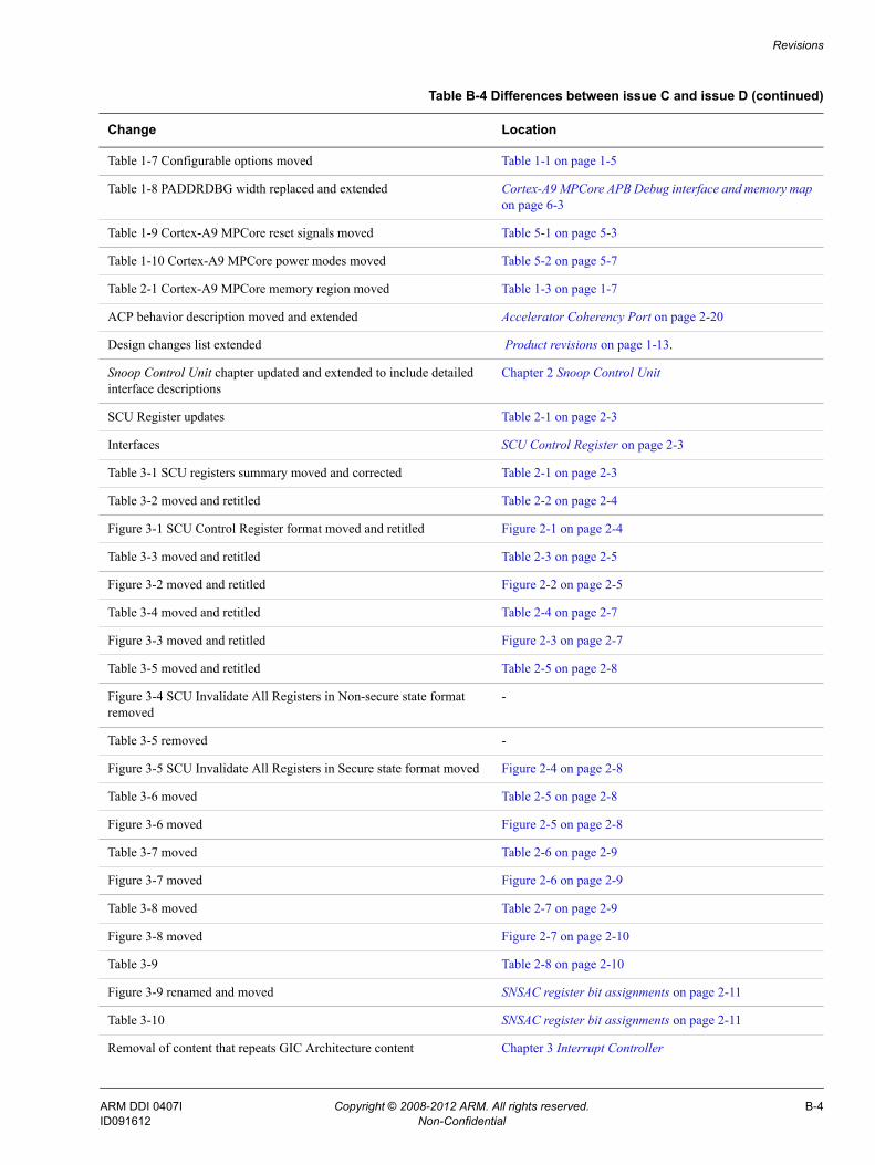
Revisions
Table 1-7 Configurable options moved Table 1-1 on page 1-5
Table 1-8 PADDRDBG width replaced and extended Cortex-A9 MPCore APB Debug interface and memory map on page 6-3
Table 1-9 Cortex-A9 MPCore reset signals moved Table 5-1 on page 5-3
Table 1-10 Cortex-A9 MPCore power modes moved Table 5-2 on page 5-7
Table 2-1 Cortex-A9 MPCore memory region moved Table 1-3 on page 1-7
ACP behavior description moved and extended Accelerator Coherency Port on page 2-20
Design changes list extended Product revisions on page 1-13.
Snoop Control Unit chapter updated and extended to include detailed interface descriptions
Chapter 2 Snoop Control Unit
SCU Register updates Table 2-1 on page 2-3
Interfaces SCU Control Register on page 2-3
Table 3-1 SCU registers summary moved and corrected Table 2-1 on page 2-3
Table 3-2 moved and retitled Table 2-2 on page 2-4
Figure 3-1 SCU Control Register format moved and retitled Figure 2-1 on page 2-4
Table 3-3 moved and retitled Table 2-3 on page 2-5
Figure 3-2 moved and retitled Figure 2-2 on page 2-5
Table 3-4 moved and retitled Table 2-4 on page 2-7
Figure 3-3 moved and retitled Figure 2-3 on page 2-7
Table 3-5 moved and retitled Table 2-5 on page 2-8
Figure 3-4 SCU Invalidate All Registers in Non-secure state format removed
-
Table 3-5 removed -
Figure 3-5 SCU Invalidate All Registers in Secure state format moved Figure 2-4 on page 2-8
Table 3-6 moved Table 2-5 on page 2-8
Figure 3-6 moved Figure 2-5 on page 2-8
Table 3-7 moved Table 2-6 on page 2-9
Figure 3-7 moved Figure 2-6 on page 2-9
Table 3-8 moved Table 2-7 on page 2-9
Figure 3-8 moved Figure 2-7 on page 2-10
Table 3-9 Table 2-8 on page 2-10
Figure 3-9 renamed and moved SNSAC register bit assignments on page 2-11
Table 3-10 SNSAC register bit assignments on page 2-11
Removal of content that repeats GIC Architecture content Chapter 3 Interrupt Controller
Table B-4 Differences between issue C and issue D (continued)
Change Location
ARM DDI 0407I Copyright © 2008-2012 ARM. All rights reserved. B-4ID091612 Non-Confidential
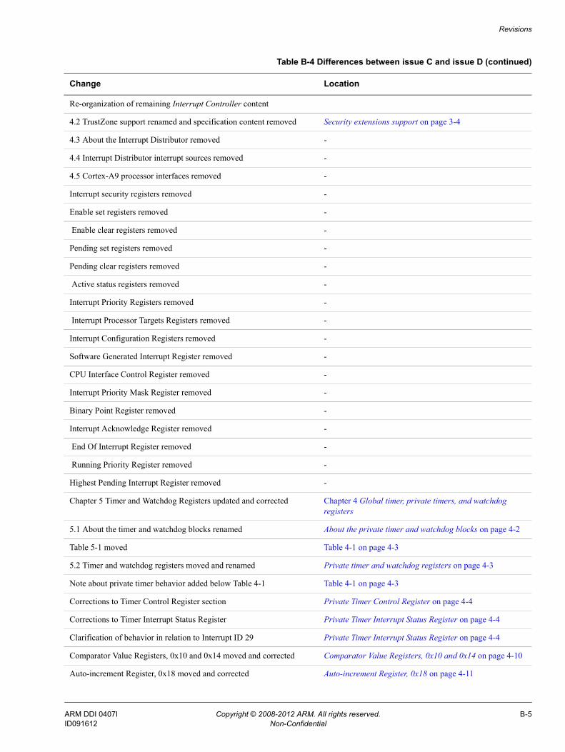
Revisions
Re-organization of remaining Interrupt Controller content
4.2 TrustZone support renamed and specification content removed Security extensions support on page 3-4
4.3 About the Interrupt Distributor removed -
4.4 Interrupt Distributor interrupt sources removed -
4.5 Cortex-A9 processor interfaces removed -
Interrupt security registers removed -
Enable set registers removed -
Enable clear registers removed -
Pending set registers removed -
Pending clear registers removed -
Active status registers removed -
Interrupt Priority Registers removed -
Interrupt Processor Targets Registers removed -
Interrupt Configuration Registers removed -
Software Generated Interrupt Register removed -
CPU Interface Control Register removed -
Interrupt Priority Mask Register removed -
Binary Point Register removed -
Interrupt Acknowledge Register removed -
End Of Interrupt Register removed -
Running Priority Register removed -
Highest Pending Interrupt Register removed -
Chapter 5 Timer and Watchdog Registers updated and corrected Chapter 4 Global timer, private timers, and watchdog registers
5.1 About the timer and watchdog blocks renamed About the private timer and watchdog blocks on page 4-2
Table 5-1 moved Table 4-1 on page 4-3
5.2 Timer and watchdog registers moved and renamed Private timer and watchdog registers on page 4-3
Note about private timer behavior added below Table 4-1 Table 4-1 on page 4-3
Corrections to Timer Control Register section Private Timer Control Register on page 4-4
Corrections to Timer Interrupt Status Register Private Timer Interrupt Status Register on page 4-4
Clarification of behavior in relation to Interrupt ID 29 Private Timer Interrupt Status Register on page 4-4
Comparator Value Registers, 0x10 and 0x14 moved and corrected Comparator Value Registers, 0x10 and 0x14 on page 4-10
Auto-increment Register, 0x18 moved and corrected Auto-increment Register, 0x18 on page 4-11
Table B-4 Differences between issue C and issue D (continued)
Change Location
ARM DDI 0407I Copyright © 2008-2012 ARM. All rights reserved. B-5ID091612 Non-Confidential
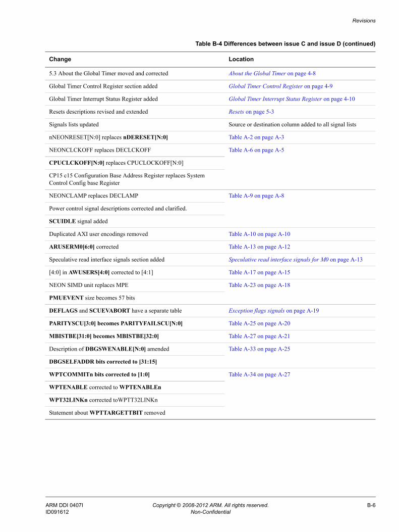
Revisions
5.3 About the Global Timer moved and corrected About the Global Timer on page 4-8
Global Timer Control Register section added Global Timer Control Register on page 4-9
Global Timer Interrupt Status Register added Global Timer Interrupt Status Register on page 4-10
Resets descriptions revised and extended Resets on page 5-3
Signals lists updated Source or destination column added to all signal lists
nNEONRESET[N:0] replaces nDERESET[N:0] Table A-2 on page A-3
NEONCLCKOFF replaces DECLCKOFF Table A-6 on page A-5
CPUCLCKOFF[N:0] replaces CPUCLOCKOFF[N:0]
CP15 c15 Configuration Base Address Register replaces System Control Config base Register
NEONCLAMP replaces DECLAMP Table A-9 on page A-8
Power control signal descriptions corrected and clarified.
SCUIDLE signal added
Duplicated AXI user encodings removed Table A-10 on page A-10
ARUSERM0[6:0] corrected Table A-13 on page A-12
Speculative read interface signals section added Speculative read interface signals for M0 on page A-13
[4:0] in AWUSERS[4:0] corrected to [4:1] Table A-17 on page A-15
NEON SIMD unit replaces MPE Table A-23 on page A-18
PMUEVENT size becomes 57 bits
DEFLAGS and SCUEVABORT have a separate table Exception flags signals on page A-19
PARITYSCU[3:0] becomes PARITYFAILSCU[N:0] Table A-25 on page A-20
MBISTBE[31:0] becomes MBISTBE[32:0] Table A-27 on page A-21
Description of DBGSWENABLE[N:0] amended Table A-33 on page A-25
DBGSELFADDR bits corrected to [31:15]
WPTCOMMITn bits corrected to [1:0] Table A-34 on page A-27
WPTENABLE corrected to WPTENABLEn
WPT32LINKn corrected toWPTT32LINKn
Statement about WPTTARGETTBIT removed
Table B-4 Differences between issue C and issue D (continued)
Change Location
ARM DDI 0407I Copyright © 2008-2012 ARM. All rights reserved. B-6ID091612 Non-Confidential

Revisions
Table B-5 Differences between D and F
Document title corrected to AMBA® Level 2 Cache Controller (L2C-310) Technical Reference Manual
Additional reading on page viii
PL310 corrected to L2C-310 throughout -
Symmetric configurations corrected to uniform configurations About the Cortex-A9 MPCore processor on page 1-2
Tag RAMs renamed to Cache line directory Figure 1-1 on page 1-3
Coherency description reworded for clarity About Cortex-A9 MPCore coherency on page 1-10
SCU control register corrections SCU Control Register on page 2-3
Values corrected Table 2-10 on page 2-13
Note about theoretical maximums added AXI issuing capabilities on page 2-13
Corrections to INCR values Cortex-A9 MPCore AXI transactions on page 2-14
Note about transactions added
Data linefill buffer corrected Table 2-11 on page 2-14
Clarification about ratios added AXI master interface clocking on page 2-18
Removed incorrect cross references Chapter 3 Interrupt Controller
Register names aligned with GIC Architecture names Chapter 3 Interrupt Controller
Access description corrected About the Interrupt Controller on page 3-2
Corrected information about interrupt sources Interrupt Distributor interrupt sources on page 3-2
Paragraph about single processor designs moved Interrupt Processor Targets Registers on page 3-9
Second line corrected Table 3-1 on page 3-5
Interrupt Configuration Registers section added Interrupt Configuration Registers on page 3-10
Values column added to Table 3-5 Table 3-5 on page 3-9
Inputs clarified. PPI Status Register on page 3-10
Address offset sentence below Figure 3-6 removed Figure 3-6 on page 3-11
PrimeCell Identification Registers section removed -
Description of prescaler added to features list About the private timer and watchdog blocks on page 4-2
PERIPHCLK added as reference clock Private Timer Control Register on page 4-4
Global timer behavior feature added About the Global Timer on page 4-8
Comparator register offsets added Comparator Value Registers, 0x10 and 0x14 on page 4-10
No asynchronous interfaces information added Clocks on page 5-2
Reset descriptions expanded and clarified Resets on page 5-3
IEM section removed Power management on page 5-7
ARM DDI 0407I Copyright © 2008-2012 ARM. All rights reserved. B-7ID091612 Non-Confidential
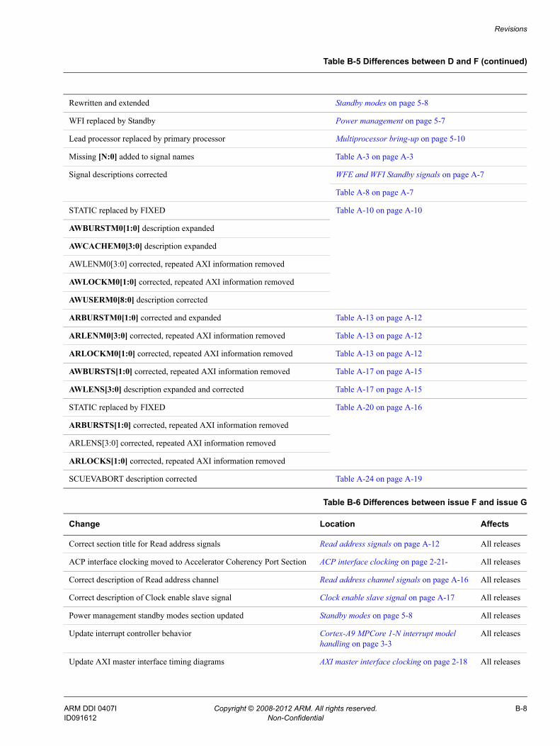
Revisions
Rewritten and extended Standby modes on page 5-8
WFI replaced by Standby Power management on page 5-7
Lead processor replaced by primary processor Multiprocessor bring-up on page 5-10
Missing [N:0] added to signal names Table A-3 on page A-3
Signal descriptions corrected WFE and WFI Standby signals on page A-7
Table A-8 on page A-7
STATIC replaced by FIXED Table A-10 on page A-10
AWBURSTM0[1:0] description expanded
AWCACHEM0[3:0] description expanded
AWLENM0[3:0] corrected, repeated AXI information removed
AWLOCKM0[1:0] corrected, repeated AXI information removed
AWUSERM0[8:0] description corrected
ARBURSTM0[1:0] corrected and expanded Table A-13 on page A-12
ARLENM0[3:0] corrected, repeated AXI information removed Table A-13 on page A-12
ARLOCKM0[1:0] corrected, repeated AXI information removed Table A-13 on page A-12
AWBURSTS[1:0] corrected, repeated AXI information removed Table A-17 on page A-15
AWLENS[3:0] description expanded and corrected Table A-17 on page A-15
STATIC replaced by FIXED Table A-20 on page A-16
ARBURSTS[1:0] corrected, repeated AXI information removed
ARLENS[3:0] corrected, repeated AXI information removed
ARLOCKS[1:0] corrected, repeated AXI information removed
SCUEVABORT description corrected Table A-24 on page A-19
Table B-6 Differences between issue F and issue G
Change Location Affects
Correct section title for Read address signals Read address signals on page A-12 All releases
ACP interface clocking moved to Accelerator Coherency Port Section ACP interface clocking on page 2-21- All releases
Correct description of Read address channel Read address channel signals on page A-16 All releases
Correct description of Clock enable slave signal Clock enable slave signal on page A-17 All releases
Power management standby modes section updated Standby modes on page 5-8 All releases
Update interrupt controller behavior Cortex-A9 MPCore 1-N interrupt model handling on page 3-3
All releases
Update AXI master interface timing diagrams AXI master interface clocking on page 2-18 All releases
Table B-5 Differences between D and F (continued)
ARM DDI 0407I Copyright © 2008-2012 ARM. All rights reserved. B-8ID091612 Non-Confidential
Revisions
Updated SCU register summary table to include security state Table 2-1 on page 2-3 All releases
Updated information about Tag RAM sizes Table 2-3 on page 2-5 All releases
Updated description of SCU Invalidate All Registers in Secure State SCU Invalidate All Registers in Secure State Register on page 2-7
All releases
Updated description of SAC and SNSAC Table 2-8 on page 2-10Table 2-9 on page 2-11
All releases
Updated description of ACP functional limitations ACP functional limitations on page 2-22 All releases
Updated interrupt controller description About the Interrupt Controller on page 3-2Interrupt Distributor interrupt sources on page 3-2Interrupt Distributor arbitration on page 3-3
All releases
Updated ICDDCR usage constraints Distributor Control Register on page 3-6 All releases
Updated SCU CPU Power Status Register reset value Table 2-2 on page 2-4 All releases
Table B-6 Differences between issue F and issue G (continued)
Change Location Affects
Table B-7 Differences between issue G and issue H
Change Location Affects
Updated configuration options for TLB, BTAC and GHB sizes, and the number of entries in the Instruction micro TLB
Table 1-1 on page 1-5 r4p0
Updated Interrupt Priority Registers in Distributor register summary Table 3-1 on page 3-5 All releases
Table B-8 Differences between issue H and issue I
Change Location Affects
Revision number changes only. - r4p1
ARM DDI 0407I Copyright © 2008-2012 ARM. All rights reserved. B-9ID091612 Non-Confidential