contamination control
TRANSCRIPT

EBB 323 Semiconductor Fabrication Technology
Contamination control
Dr Khairunisak Abdul RazakRoom 2.16School of Material and Mineral Resources EngineeringUniversiti Sains [email protected]
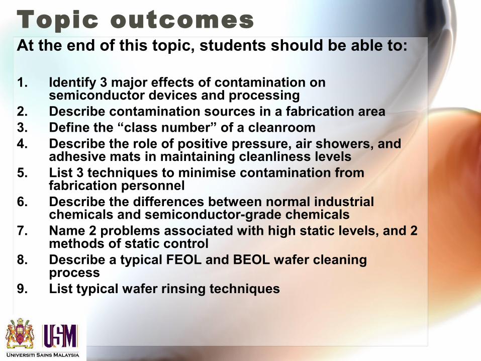
Topic outcomesAt the end of this topic, students should be able to:
1. Identify 3 major effects of contamination on semiconductor devices and processing
2. Describe contamination sources in a fabrication area3. Define the “class number” of a cleanroom4. Describe the role of positive pressure, air showers, and
adhesive mats in maintaining cleanliness levels5. List 3 techniques to minimise contamination from
fabrication personnel6. Describe the differences between normal industrial
chemicals and semiconductor-grade chemicals7. Name 2 problems associated with high static levels, and 2
methods of static control8. Describe a typical FEOL and BEOL wafer cleaning
process9. List typical wafer rinsing techniques

Cause of contamination
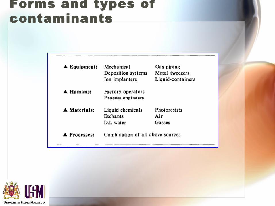
Forms and types of contaminants
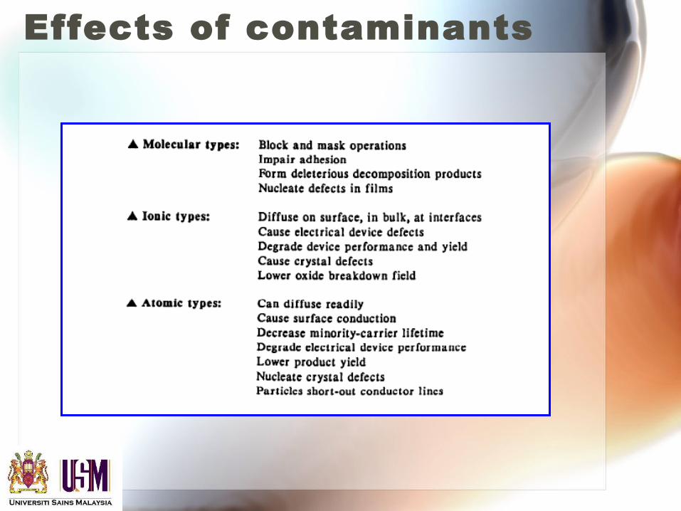
Effects of contaminants
5 major classes of contaminants1. Particles
2. Metallic ions
3. Chemicals
4. Bacteria
5. Airborne molecular contaminants (AMCs)
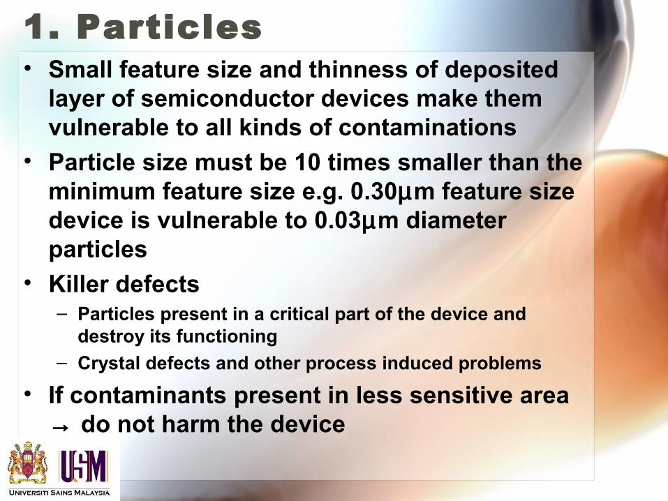
1. Particles • Small feature size and thinness of deposited
layer of semiconductor devices make them vulnerable to all kinds of contaminations
• Particle size must be 10 times smaller than the minimum feature size e.g. 0.30µm feature size device is vulnerable to 0.03µm diameter particles
• Killer defects– Particles present in a critical part of the device and
destroy its functioning– Crystal defects and other process induced problems
• If contaminants present in less sensitive area → do not harm the device

Relative sizes
Relative size of contamination
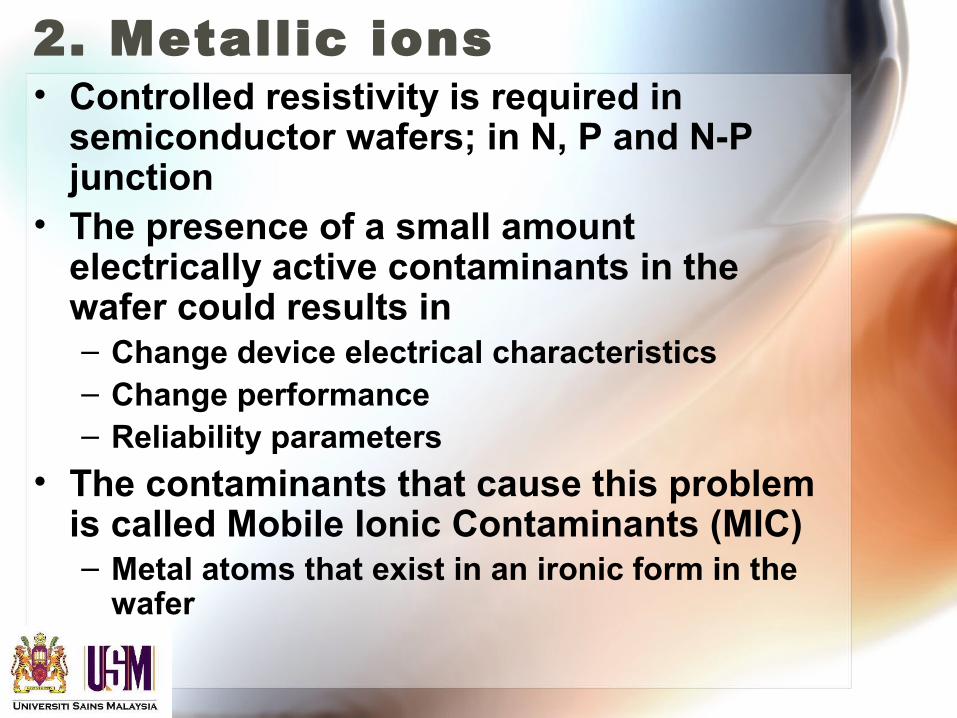
2. Metallic ions• Controlled resistivity is required in
semiconductor wafers; in N, P and N-P junction
• The presence of a small amount electrically active contaminants in the wafer could results in– Change device electrical characteristics– Change performance– Reliability parameters
• The contaminants that cause this problem is called Mobile Ionic Contaminants (MIC)– Metal atoms that exist in an ironic form in the
wafer
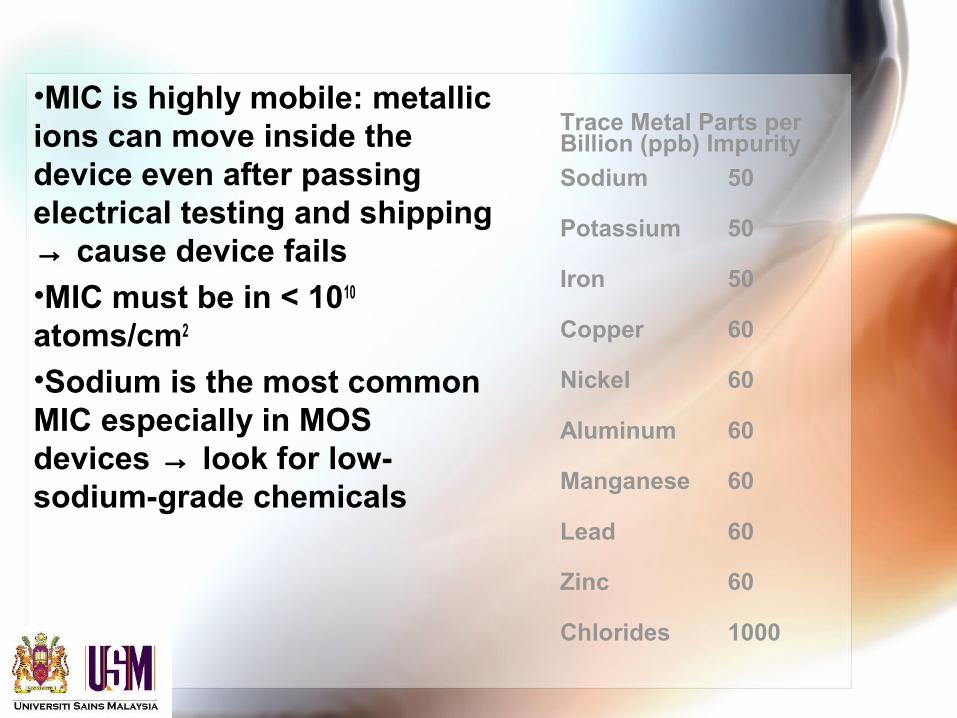
•MIC is highly mobile: metallic ions can move inside the device even after passing electrical testing and shipping → cause device fails•MIC must be in < 1010 atoms/cm2
•Sodium is the most common MIC especially in MOS devices → look for low-sodium-grade chemicals
Trace Metal Parts per Billion (ppb) Impurity
Sodium 50
Potassium 50
Iron 50
Copper 60
Nickel 60
Aluminum 60
Manganese 60
Lead 60
Zinc 60
Chlorides 1000
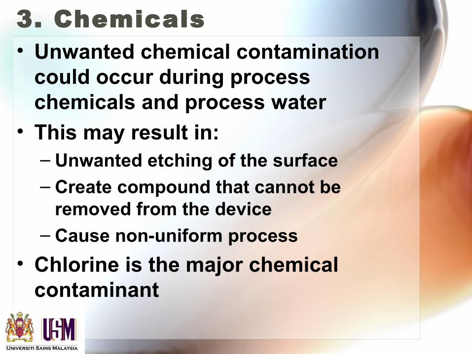
3. Chemicals • Unwanted chemical contamination
could occur during process chemicals and process water
• This may result in: – Unwanted etching of the surface– Create compound that cannot be
removed from the device – Cause non-uniform process
• Chlorine is the major chemical contaminant
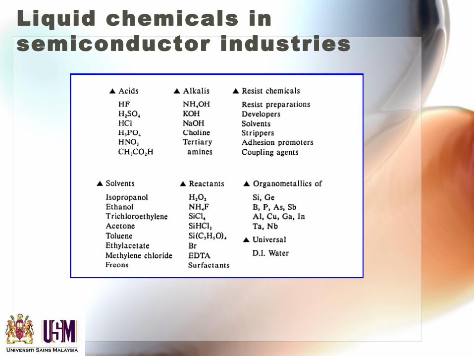
Liquid chemicals in semiconductor industries
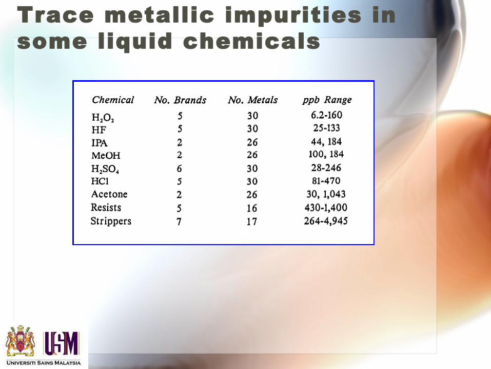
Trace metallic impurities in some liquid chemicals
4. Bacteria• Can be defined as organisms that
grow in water systems or on surfaces that are not cleaned regularly
• On semiconductor device, bacteria acts as particulate contamination or may contribute unwanted metallic ions to the device surface
5. Airborne molecular contaminants (AMCs)• AMCs- fugitive molecules that escape from process tools,
chemical delivery systems, or are carried out into a fabrication area on materials or personnel
• AMCs: gasses, dopants, and process chemicals used in fabrication area e.g. oxygen, moisture, organics, acids, bases etc..
• Problems:– Harmful to process that requires delicate chemical
reactions such as the exposure of photoresist in the patterning operations
– Shift etch rates– Unwanted dopants that shift device electrical parameters – Change the wetting characteristics of etchants leading to
incomplete etching
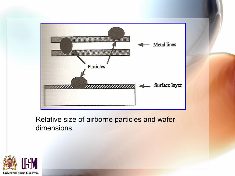
Relative size of airborne particles and wafer dimensions
The effects of contamination on semiconductor devices1. Device processing yield
- contaminants may change the dimensions device parts
- change cleanliness of the surfaces
- pitted layers
⇒ reduce overall yield through various quality checks
2. Device performance
- This may due to the presence of small pieces of contamination that is not detectable during quality checks
- may also come from unwanted chemicals or AMCs in the process steps ⇒ alter device dimensions or material quality
- high amount of mobile ionic contaminants in the wafer can change the electrical performance of the device
3. Device reliability- Failure of device due to the presence of a small amount of metallic contaminants that get into the wafer during processing and not detected during device testing. These contaminants can travel inside the device and end up in electrically sensitive areas and cause device failure
Contamination sources1. Air
2. The production facility
3. Cleanroom personnel
4. Process water
5. Process chemicals
6. Process gasses
7. Static charge
1. Air• Normal air contains contaminants → must be
treated before entering a cleanroom• Major contaminant is airborne particles;
particulates or aerosols– They float and remain in air for long period of
time• Air cleanliness levels of cleanroom is determined
by the – Particulate diameters– Density in air
• Federal standard 209E: class number of the air in the area– Number of particles 0.5µm or larger in a cubic foot of air
• In normal city with smoke, smog and fumes can contains up to 5 million particles per cubic foot: class number 5 million
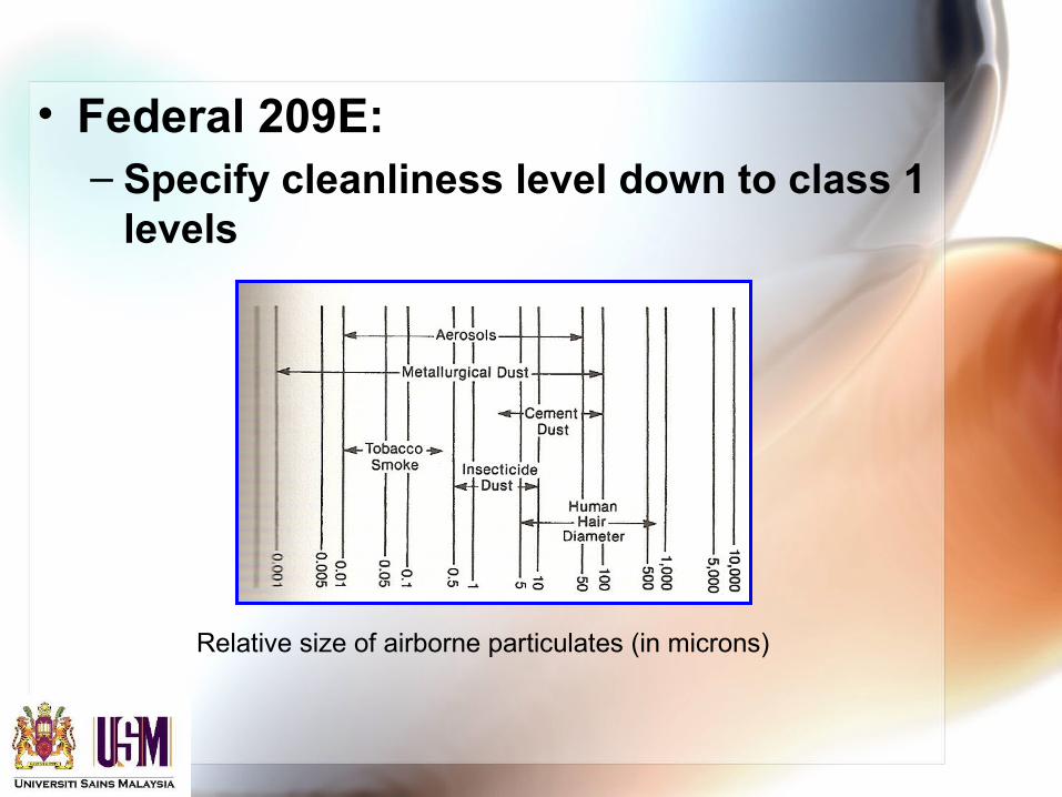
• Federal 209E:– Specify cleanliness level down to class 1
levels
Relative size of airborne particulates (in microns)
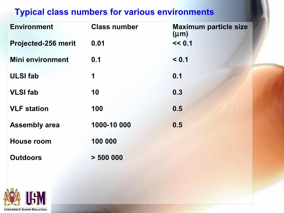
Environment Class number Maximum particle size (µm)
Projected-256 merit 0.01 << 0.1
Mini environment 0.1 < 0.1
ULSI fab 1 0.1
VLSI fab 10 0.3
VLF station 100 0.5
Assembly area 1000-10 000 0.5
House room 100 000
Outdoors > 500 000
Typical class numbers for various environments
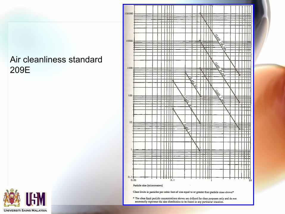
Air cleanliness standard 209E
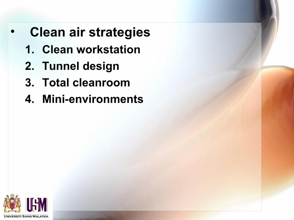
• Clean air strategies1. Clean workstation
2. Tunnel design
3. Total cleanroom
4. Mini-environments
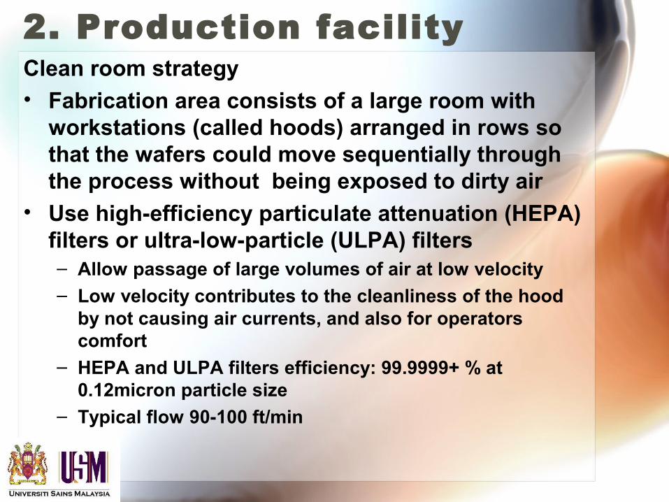
2. Production facilityClean room strategy• Fabrication area consists of a large room with
workstations (called hoods) arranged in rows so that the wafers could move sequentially through the process without being exposed to dirty air
• Use high-efficiency particulate attenuation (HEPA) filters or ultra-low-particle (ULPA) filters– Allow passage of large volumes of air at low velocity– Low velocity contributes to the cleanliness of the hood
by not causing air currents, and also for operators comfort
– HEPA and ULPA filters efficiency: 99.9999+ % at 0.12micron particle size
– Typical flow 90-100 ft/min

• HEPA and ULPA filters mounted on a clean hood– Vertical laminar flow (VLF) → air leave the
system in a laminar pattern, and at the work surface, it turns and exits the hood
– Horizontal laminar flow (HLF) → HEPA filter is placed in the back of the work surface
– Both VLF and HLF stations keep the wafer cleans:
• Filtered air inside the hood• Cleaning action inside is the slight positive pressure
built up in the station → prevent airborne dirt from operators and from aisle area from entering the hood
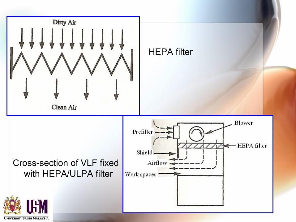
Cross-section of VLF fixed with HEPA/ULPA filter
HEPA filter
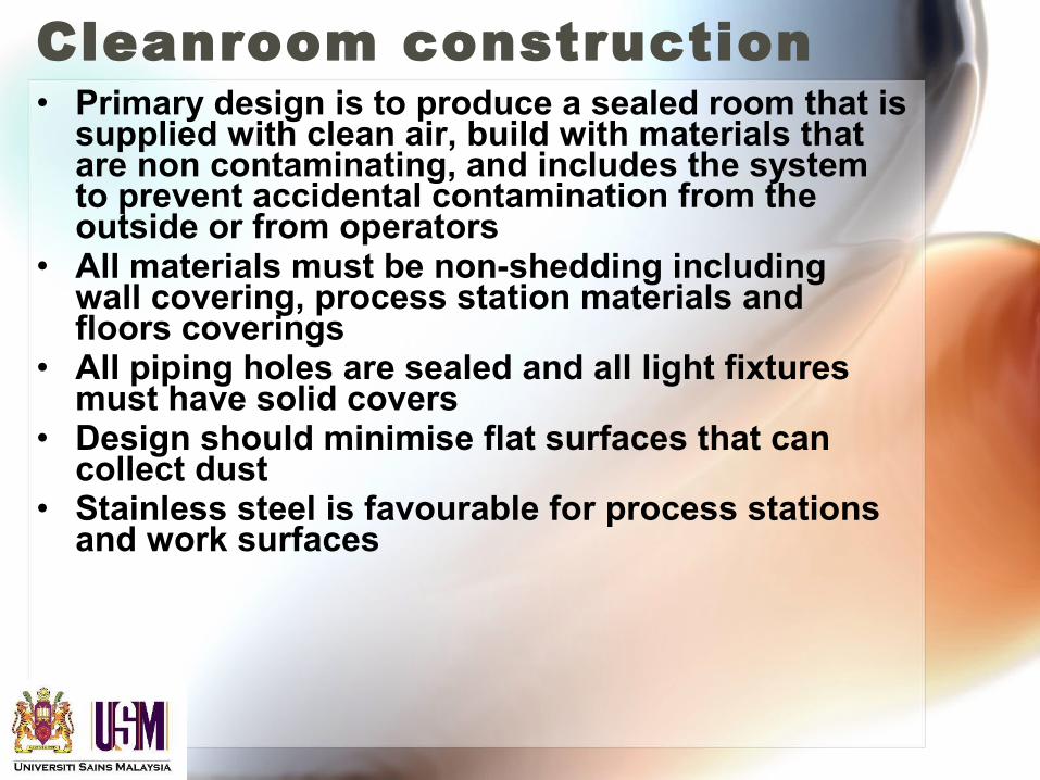
Cleanroom construction• Primary design is to produce a sealed room that is
supplied with clean air, build with materials that are non contaminating, and includes the system to prevent accidental contamination from the outside or from operators
• All materials must be non-shedding including wall covering, process station materials and floors coverings
• All piping holes are sealed and all light fixtures must have solid covers
• Design should minimise flat surfaces that can collect dust
• Stainless steel is favourable for process stations and work surfaces
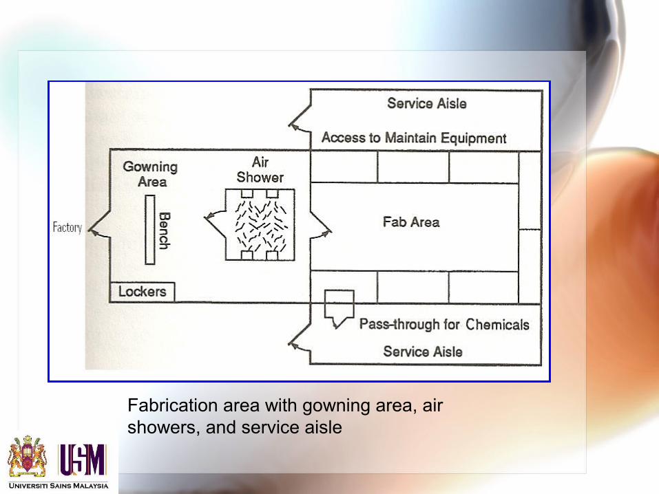
Fabrication area with gowning area, air showers, and service aisle
Cleanroom elements:1. Adhesive floor mats
– At every entrance to pull off and holds dirt adhered at the bottom of the shoes
2. Gowning area– Buffer between cleanroom and the plant– Always supply with filtered air from ceiling HEPA
filters– Store cleanroom apparel and change to
cleanroom garments
3. Air pressure– Highest pressure in cleanroom, second highest
in gowning area and the lowest in factory hallways
– Higher pressure in cleanroom causes a low flow of air out of the doors and blow airborne particle back into the dirtier hall way
4. Air showers- Air shower is located between the governing
room and the cleanroom- High velocity air jets blow off particles from the
outside of the garments- Air shower possesses interlocking system to
prevent both doors from being opened at the same time
4. Service bay- Semi-clean area for storage materials and
supplies- Service bay has Class 1000 or class 10 000- Bay area contains process chemical pipes,
electrical power lines and cleanroom materials- Critical process machines are backed up to the
wall dividing the cleanroom and the bay → allows technician to service the equipment from the back without entering the cleanroom
6. Double-door-pass-through- Simple double-door boxes or may have a supply
of positive-pressure filtered air with interlocking devices to prevent both doors from being opened at the same time
- Often fitted with HEPA filters
6. Static control
7. Static charge• Static charge → attracts smaller particles to the
wafer• The static charge may build up on wafers, storage
boxes, work surfaces and equipment– May generate up to 50 000V static charge → attract
aerosols out of the air and personal garment → contaminate the wafers
• Particles held by static charge is hard to remove using a standard brush or wet cleaning system
• Most static charge is produced by triboelectric charging– 2 materials initially in contact are separated– 1 surface possesses positive charge because it losses
electron– 1 surface becomes negative because it gains electron
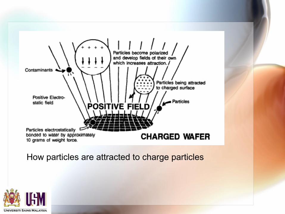
How particles are attracted to charge particles
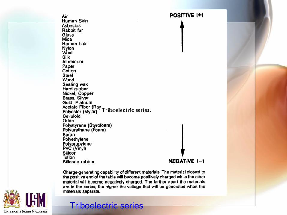
Triboelectric series
• Electrostatic Discharge (ESD): – rapid transfer of electrostatic charge between two
objects, usually resulting when two objects at different potentials come into direct contact with each other.
– ESD can also occur when a high electrostatic field develops between two objects in close proximity.
• Control static– Prevent charge build up
• Use antistatic materials in garments and in-process storage boxes
• Apply antistatic solution on certain walls to prevent charge build up- not use in critical station due to possible contamination
– Use discharge technique• Use ionisers and grounded static-discharge
Eliminating static charge:
•Air ioniser – neutralise nonconductive materials
•Grounding of conducting surfaces
•Increasing conductivity of materials
•Humidity control
•Surface treatment with topical antistat solutions
6. Shoe cleaners- Removal of dirt from the sides of shoes and
shoes cover- Rotating brushes to remove the dirt- Typical machines feature an internal vacuum to
capture the loosened dirt, and bags to hold the dirt for removal from the area
6. Glove cleaners- Discard gloves when they are contaminated or
dirty or after every shift
- Some fabrication areas use glove cleaners that clean and dry the gloves in an enclosure

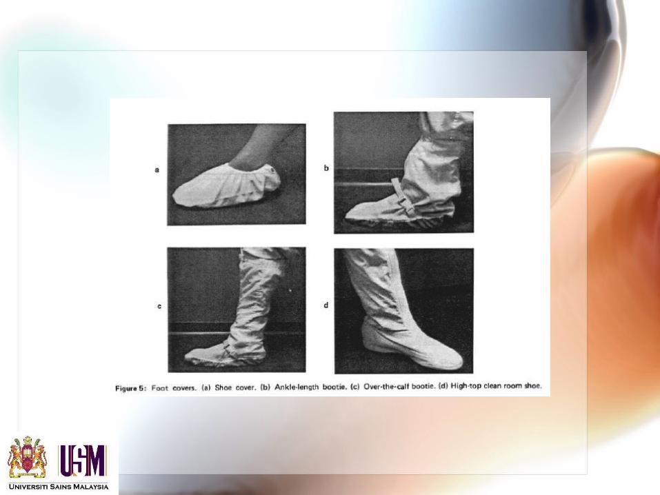
Typical cleanroom garments
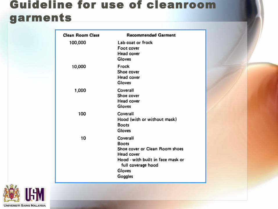
Guideline for use of cleanroom garments
3. Cleanroom personnel • Even after shower and sitting: 100 000-1
000 000 particles/minute – Increase dramatically when moving e.g.
generate 5 million particles/min with movement of 2 miles/hr
• Example of human contaminants:– Flakes of dead hair– Normal skin flaking– Hair sprays
– Cosmetics
– Facial hair– Exposed clothing

4. Process water• During fabrication process
– Repeated chemical etch and clean– Water rinse is essential after etching/ cleaning
step → several hours in the whole system• Unacceptable contaminants in normal city water
– Dissolves minerals– Particles– Bacteria – Organics– Dissolved O2
– Silica
• Dissolve minerals– Comes from salt in normal water Na+ Cl-
– Can be removed by reverse osmosis (RO) and ion exchange systems
• Remove electrically active ions → change water from conductive medium to resistive medium
• It is a must to monitor resistivity of all process water in the fabrication area– Need to obtain between 15-18 MΩ
• Remove contaminants– Solid particles: sand filtration, earth filtration, membrane– Bacteria: sterilise using UV radiation and filter out the
particles– Organics (plant & fecal materials): carbon bed filtration– Dissolved O2 & CO2: force draft decarbonators and
vacuum degasifiers
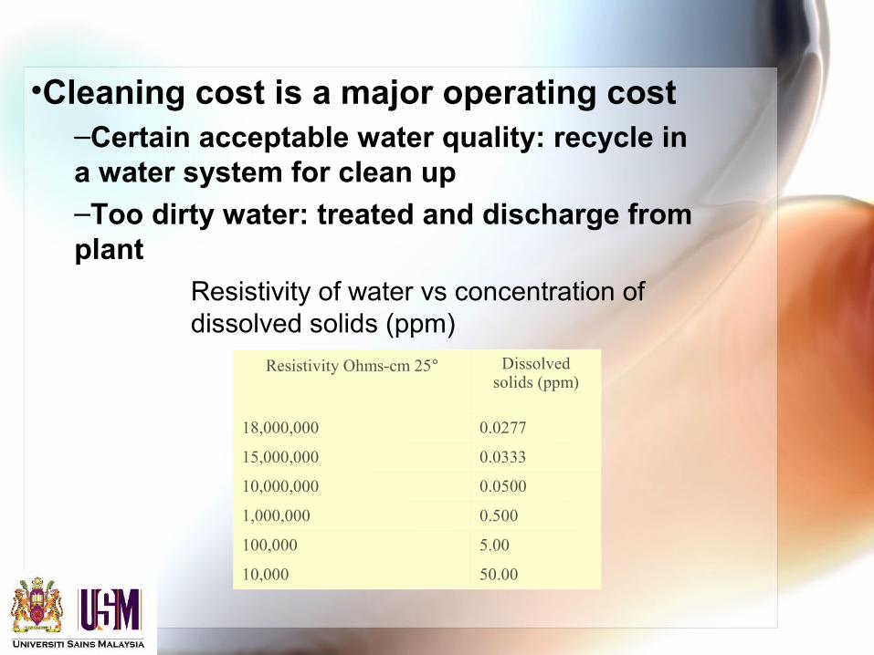
•Cleaning cost is a major operating cost–Certain acceptable water quality: recycle in a water system for clean up–Too dirty water: treated and discharge from plant
Resistivity Ohms-cm 25° Dissolved solids (ppm)
18,000,000 0.0277
15,000,000 0.0333
10,000,000 0.0500
1,000,000 0.500
100,000 5.00
10,000 50.00
Resistivity of water vs concentration of dissolved solids (ppm)

Contaminant 64Kb 1Mb 16Mb
Resistivity (MΩcm) > 17 > 18 > 18.1
TOC (micro-g/L) < 200 < 50 < 10
Bacteria (#/L) < 250 < 50 < 1
Particles < 50 < 50 < 1
Critical size (micron) 0.2 0.2 0.05
Dissolved oxygen (micron-g/L < 200 < 100 < 20
Sodium (micro-g/L) < 1 < 1 < 0.01
Chlorine (micro-g/L) < 5 < 1 < 0.01
Manganese (micro-g/L) N/A < 1 < 0.005
DRAMs water spec
5. Process chemicals• Highest purity of acids, bases and solvents are used for
etching and cleaning wafers and equipment• Chemical grades:
– Commercial– Reagent– Electronic– Semiconductor
• Main concerns: metallic mobile ionic contaminants (MIC) → must be < 1 ppm
• To date, can obtain chemicals with 1ppb MIC• Check assay no e.g. assay 99.9% purity• Other steps:
– Clean inside containers– Use containers that do not dissolve– Use particulate free labels– Place clean bottles in bags before shipping
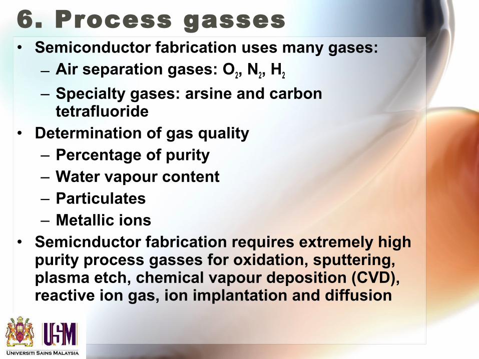
6. Process gasses• Semiconductor fabrication uses many gases:
– Air separation gases: O2, N2, H2
– Specialty gases: arsine and carbon tetrafluoride
• Determination of gas quality– Percentage of purity– Water vapour content– Particulates– Metallic ions
• Semicnductor fabrication requires extremely high purity process gasses for oxidation, sputtering, plasma etch, chemical vapour deposition (CVD), reactive ion gas, ion implantation and diffusion
• If gas is contaminated, wafer properties could be altered due to chemical reaction
• Gas quality is also shown in assay no; 99.99-99.999999. The highest quality is called “six 9s pure”
Requirements for Si wafer cleaning process1. Effective removal of all types of surface
contaminants
2. Not etching or damaging Si and SiO2
3. Use of contamination-free and volatilisation chemicals
4. Relatively safe, simple, and economical for production applications
5. Ecologically acceptable, free of toxic waste products
6. Implementable by a variety of techniques

Wafer surface cleaning4 general types of contaminants:
1. Particulates2. Organic residues3. Inorganic residues4. Unwanted oxide layers
• Wafer cleaning process must– Remove all surface contaminants– Not etch or damage the wafer surface– Be safe and economical in a production
setting– Be ecological acceptable
• 2 primary wafer conditions:1. Front end of the line (FEOL)2. Back end of the line (BEOL)
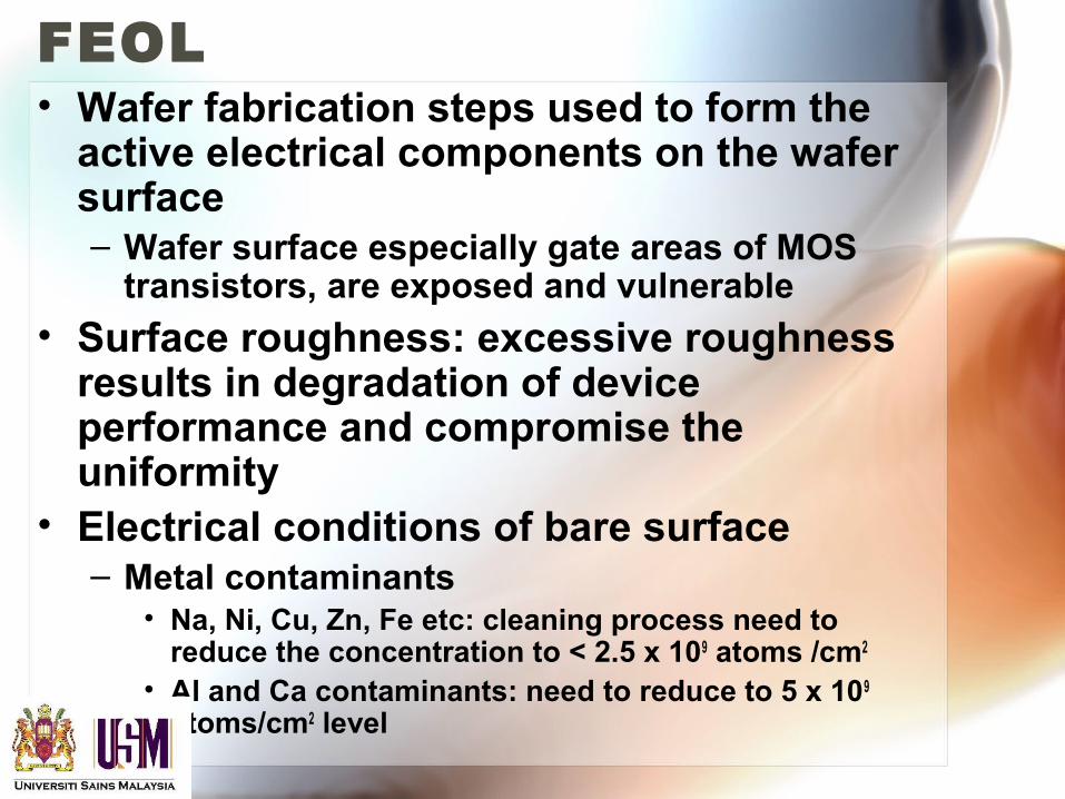
FEOL• Wafer fabrication steps used to form the
active electrical components on the wafer surface– Wafer surface especially gate areas of MOS
transistors, are exposed and vulnerable
• Surface roughness: excessive roughness results in degradation of device performance and compromise the uniformity
• Electrical conditions of bare surface– Metal contaminants
• Na, Ni, Cu, Zn, Fe etc: cleaning process need to reduce the concentration to < 2.5 x 10⁹ atoms /cm2
• Al and Ca contaminants: need to reduce to 5 x 10⁹ atoms/cm2 level
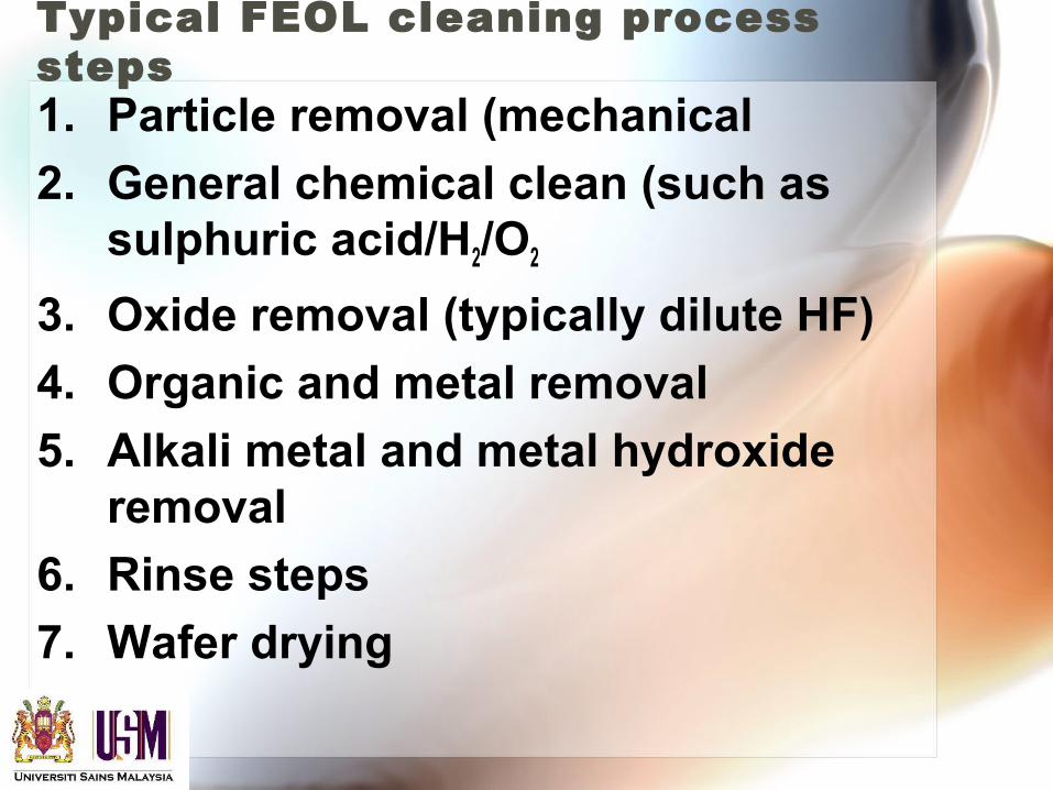
Typical FEOL cleaning process steps1. Particle removal (mechanical
2. General chemical clean (such as sulphuric acid/H2/O2
3. Oxide removal (typically dilute HF)
4. Organic and metal removal
5. Alkali metal and metal hydroxide removal
6. Rinse steps
7. Wafer drying
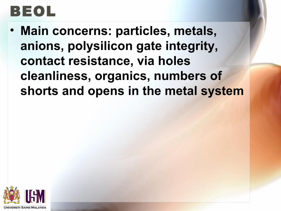
BEOL• Main concerns: particles, metals,
anions, polysilicon gate integrity, contact resistance, via holes cleanliness, organics, numbers of shorts and opens in the metal system
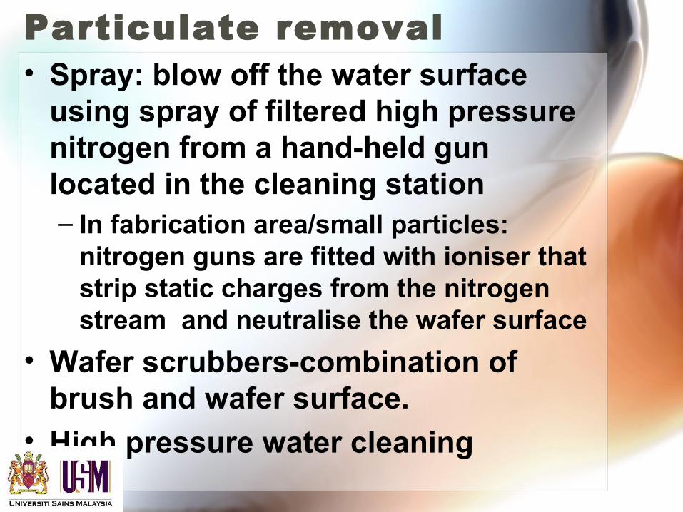
Particulate removal• Spray: blow off the water surface
using spray of filtered high pressure nitrogen from a hand-held gun located in the cleaning station– In fabrication area/small particles:
nitrogen guns are fitted with ioniser that strip static charges from the nitrogen stream and neutralise the wafer surface
• Wafer scrubbers-combination of brush and wafer surface.
• High pressure water cleaning
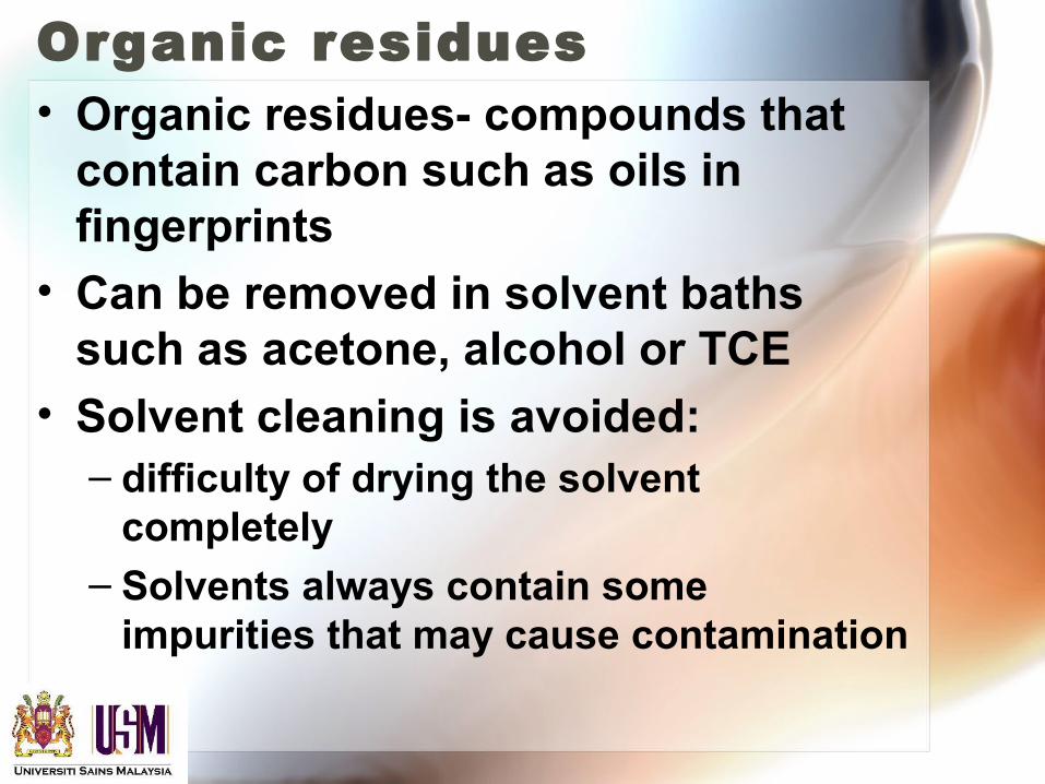
Organic residues• Organic residues- compounds that
contain carbon such as oils in fingerprints
• Can be removed in solvent baths such as acetone, alcohol or TCE
• Solvent cleaning is avoided:– difficulty of drying the solvent
completely– Solvents always contain some
impurities that may cause contamination
Inorganic residues• Organic residues- do not contain
carbon e.g. HCl and HF from steps in wafer processing
Chemical cleaning solutions• For both organic and inorganic
contaminants• General chemical cleaning
1. Sulphuric acid • Hot sulphuric acid with added oxidant• Also a general photoresist stripper
• H2SO4 is an effective cleaner in 90-125°C → remove most inorganic residues and particulates from the surface
• Oxidants are added to remove carbon residues
• Chemical reaction converts C to CO2
• Typical oxidants: hydrogen peroxide (H2O2), ammonium persulfate [(NH4)2S2O8]
• Nitric acid (HNO3), and ozone (O2)
RCA clean• RCA clean- H2O2 is used with some base
or acid• Standard clean 1 (SC-1)
– Solution of water, hydrogen peroxide, ammonium hydroxide = 5:1:1, 7:2:1, heated to 75-85°C
– SC-1 removes organic residues and set up a condition for desorption of trace metals from the surface
– Oxide films keep forming and dissolving• SC-2
– Solution of water, hydrogen peroxide and hydrochloric acid = 6:1:1 to 8:2:1, 75-85°C
– Remove alkali ions and hydroxides and complex residual metals
– Leave a protective oxide layer
• Order of SC-1 and SC-2 can be reversed
• If oxide-free surface is required, HF step is used before, in between, or after the RCA cleans