construction - veer surendra sai university of...
TRANSCRIPT
SCR and THYRISTOR
SILICON CONTROLLED RECTIFIERS (SCR)
A silicon controlled rectifier is a semiconductor device that acts as a true electronic switch. it can change alternating current and at the same time can control the amount of power fed to the load. SCR combines the features of a rectifier and a transistor.
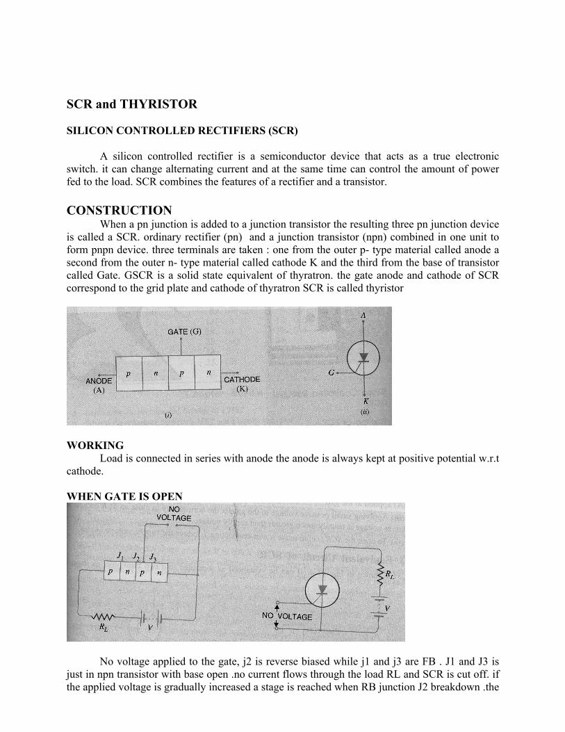
CONSTRUCTIONWhen a pn junction is added to a junction transistor the resulting three pn junction device
is called a SCR. ordinary rectifier (pn) and a junction transistor (npn) combined in one unit to form pnpn device. three terminals are taken : one from the outer p type material called anode a second from the outer n type material called cathode K and the third from the base of transistor called Gate. GSCR is a solid state equivalent of thyratron. the gate anode and cathode of SCR correspond to the grid plate and cathode of thyratron SCR is called thyristor
WORKINGLoad is connected in series with anode the anode is always kept at positive potential w.r.t
cathode.
WHEN GATE IS OPEN
No voltage applied to the gate, j2 is reverse biased while j1 and j3 are FB . J1 and J3 is just in npn transistor with base open .no current flows through the load RL and SCR is cut off. if the applied voltage is gradually increased a stage is reached when RB junction J2 breakdown .the
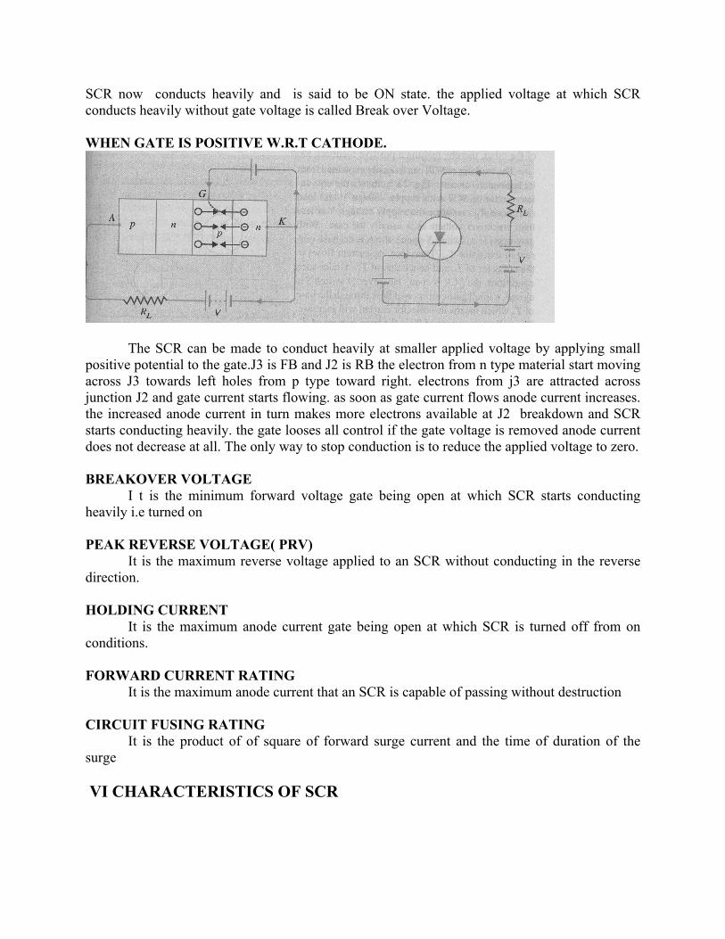
SCR now conducts heavily and is said to be ON state. the applied voltage at which SCR conducts heavily without gate voltage is called Break over Voltage.
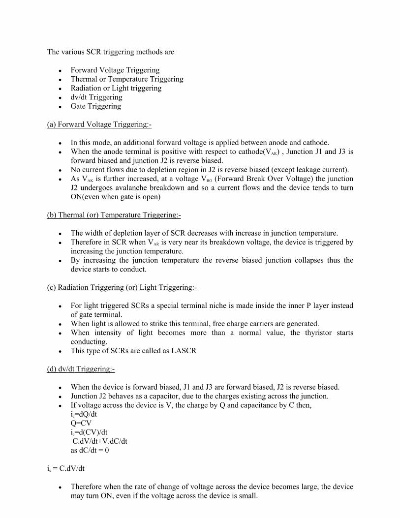
WHEN GATE IS POSITIVE W.R.T CATHODE.
The SCR can be made to conduct heavily at smaller applied voltage by applying small positive potential to the gate.J3 is FB and J2 is RB the electron from n type material start moving across J3 towards left holes from p type toward right. electrons from j3 are attracted across junction J2 and gate current starts flowing. as soon as gate current flows anode current increases. the increased anode current in turn makes more electrons available at J2 breakdown and SCR starts conducting heavily. the gate looses all control if the gate voltage is removed anode current does not decrease at all. The only way to stop conduction is to reduce the applied voltage to zero.
BREAKOVER VOLTAGE I t is the minimum forward voltage gate being open at which SCR starts conducting
heavily i.e turned on
PEAK REVERSE VOLTAGE( PRV)It is the maximum reverse voltage applied to an SCR without conducting in the reverse
direction.
HOLDING CURRENT It is the maximum anode current gate being open at which SCR is turned off from on
conditions.
FORWARD CURRENT RATING It is the maximum anode current that an SCR is capable of passing without destruction
CIRCUIT FUSING RATINGIt is the product of of square of forward surge current and the time of duration of the
surge
VI CHARACTERISTICS OF SCR

FORWARD CHARCTERISTICS
When anode is +ve w.r.t cathode the curve between V & I is called Forward characteristics. OABC is the forward characteristics of the SCR at Ig =0. if the supplied voltage is increased from zero point A is reached .SCR starts conducting voltage across SCR suddenly drops (dotted curve AB) most of supply voltage appears across RL
REVERSE CHARCTERISTICS
When anode is –ve w.r.t.cathode the curve b/w V&I is known as reverse characteristics reverse voltage come across SCR when it is operated with ac supply reverse voltage is increased anode current remains small avalanche breakdown occurs and SCR starts conducting heavily is known as reverse breakdown voltage
SCR as a switchSCR Half and Full wave rectifier
ApplicationSCR as a static contactorSCR for power controlSCR for speed control of d. c. shunt motorOver light detector
Triggering (Turn on) Methods of Thyristor:
Triggering:The turning on Process of the SCR is known as Triggering. In other words, turning the SCR from ForwardBlocking state to ForwardConduction state is known as Triggering.The various methods of SCR triggering are discussed here.
The various SCR triggering methods are
Forward Voltage Triggering Thermal or Temperature Triggering Radiation or Light triggering dv/dt Triggering Gate Triggering
(a) Forward Voltage Triggering:
In this mode, an additional forward voltage is applied between anode and cathode. When the anode terminal is positive with respect to cathode(VAK) , Junction J1 and J3 is
forward biased and junction J2 is reverse biased. No current flows due to depletion region in J2 is reverse biased (except leakage current). As VAK is further increased, at a voltage VBO (Forward Break Over Voltage) the junction
J2 undergoes avalanche breakdown and so a current flows and the device tends to turn ON(even when gate is open)
(b) Thermal (or) Temperature Triggering:
The width of depletion layer of SCR decreases with increase in junction temperature. Therefore in SCR when VAR is very near its breakdown voltage, the device is triggered by
increasing the junction temperature. By increasing the junction temperature the reverse biased junction collapses thus the
device starts to conduct.
(c) Radiation Triggering (or) Light Triggering:
For light triggered SCRs a special terminal niche is made inside the inner P layer instead of gate terminal.
When light is allowed to strike this terminal, free charge carriers are generated. When intensity of light becomes more than a normal value, the thyristor starts
conducting. This type of SCRs are called as LASCR
(d) dv/dt Triggering:
When the device is forward biased, J1 and J3 are forward biased, J2 is reverse biased. Junction J2 behaves as a capacitor, due to the charges existing across the junction. If voltage across the device is V, the charge by Q and capacitance by C then,
ic=dQ/dt Q=CVic=d(CV)/dt C.dV/dt+V.dC/dtas dC/dt = 0
ic = C.dV/dt
Therefore when the rate of change of voltage across the device becomes large, the device may turn ON, even if the voltage across the device is small.
(e) Gate Triggering:
This is most widely used SCR triggering method. Applying a positive voltage between gate and cathode can Turn ON a forward biased
thyristor. When a positive voltage is applied at the gate terminal, charge carriers are injected in the
inner Player, thereby reducing the depletion layer thickness. As the applied voltage increases, the carrier injection increases, therefore the voltage at
which forward breakover occurs decreases.
COMMUTATION OF SCR
The term commutation basically means the transfer of current from one path to another.
I t i s n o t p o s s i b l e f o r a t h y r i s t o r t o t u r n i t s e l f O F F t h e circuit in which it is connected must reduce the thyristor current to zero to enable it to turn off ‘COMMUTATION’is the term to describe the methodsof achieving this.Broadly classified into two methods:
1 .NATURAL COMMUTATION2 .FORCED COMMUTATION
NATURAL COMMUTATION This widely used method of commutation makes use of thealternating, reversing nature of a.c voltage to effect the currentt r an s f e r . As t he cu r r en t pa s se s t h rough na tu r a l z e ro , a r eve r s ev o l t a g e w i l l s i m u l t a n e o u s l y a p p e a r a c r o s s t h e d e v i c e . T h i s i m m e d i a t e l y t u r n s o f f t h e d e v i c e . T h i s p r o c e s s i s c a l l e d a s natural commutation since no external circuit is required for this purpose.FORCED COMMUTATION In case of dc circuits, for switching off the thyristors, the f o rwa rd cu r r en t shou ld be fo r ced t o be ze ro by means o f some external circuits. The process is called forced commutation.
C L A S S I F I C A T I O N O F F R O C E D C O M M U T A T I O N TECHNIQUES:T h e c l a s s i f i c a t i o n i s b a s e d o n t h e a r r a n g e m e n t o f commutating components and the manner in which zero currentis obtained in the SCR.The six distinct classes by which the SCR can be turned off are:Class A Self commutated by a resonating loadClass B Self commutated by a LC circuitClass C C or LC switched by another load carrying SCR Complementary commutationClass D C or LC switched by an auxiliary SCR Auxiliary commutationClass E An external pulse source for commutationExternal pulse commutationClass F AC line commutationClass A, Self commutated by resonating the load
•When the SCR is triggered, anode current flows and charges up C with the dot as positive.•The LCR form a second order underdamped circuit. The current through the SCR builds up and completes a half cycle.•When the inductor current will then attempt to flow through the SCR in the reverse direction and the SCR will be turned off.
Class B, Self commutated by an LC circuit
•T h e C a p a c i t o r C c h a r g e s u p i n t h e d o t a s p o s i t i v e before a gate pulse is applied to the SCR. When SCR istriggered, the resulting current has two components.•T h e c o n s t a n t l o a d c u r r e n t I f l o w s t h r o u g h R L load . Th i s i s en su red by t he l a rge r eac t ance i n s e r i e s w i th the load and the freewheeling diode clamping it.•A s i nuso ida l cu r r en t f l ows t h rough t he r e sonan t L Ccircuit to chargeup C with the dot as negative at the end of the half cycle.
•T h i s c u r r e n t w i l l t h e n r e v e r s e a n d f l o w t h r o u g h t h e SCR in opposition to the load current for a small fraction of t he nega t i ve sw ing t i l l t h e t o t a l cu r r en t t h rough t he SCR becomes zero.•T h e S C R w i l l t u r n o f f w h e n t h e r e s o n a n t – c i r c u i t (reverse) current is just greater than the load current.•T h e S C R i s t u r n e d o f f i f t h e S C R r e m a i n s r e v e r s e d biased for tq> toff , a n d t h e r a t e o f r i s e o f t h e r e a p p l i e d voltage < the rated value.
Class C, C or LC switched by another load–carrying SCR –Complementary commutation
• This configuration has two SCRs. One of them may be them a i n S C R a n d t h e o t h e r a u x i l i a r y . B o t h m a y b e l o a d c u r r e n t c a r r y i n g m a i n S C R s . T h e i n t e g r a l c o n v e r t e r supplied from a current source.•Assume SCR 2i s c o n d u c t i n g . C t h e n c h a r g e s u p i n t h e polarity shown. When SCR 1i s t r i g g e r e d , C i s s w i t c h e d across SCR 2 v i a SCR 1and t h i s c ause s t he r eve r s e vo l t ageacross SCR 2and immediately turns it off.
•Charging of capacitor C now takes place through the loada n d i t s p o l a r i t y b e c o m e s r e v e r s e . H e n c e w h e n S C R 2 is t r i gge red , C i s sw i t ched ac ro s s SCR 1 v i a SCR 2.
Now, t he reverse voltage appears across SCR 1and immediately turnsit off.
•SCR A mus t be t r i gge red f i r s t i n o rde r t o cha rge t he uppe r t e r m i n a l o f t h e c a p a c i t o r a s p o s i t i v e . A s s o o n a s C i s charged to the
supply voltage, SCR A will turn off.•When SCR M i s t r i g g e r e d t h e c u r r e n t f l o w s i n t w o p a t h s : Load current flows through the load and the commutatingcurrent flows through C SCR M LD network. The chargeon C is reversed and held at that level by the diode D.•When SCR A i s r e t r i gge red , t he vo l t age ac ro s s C appea r sacross SCR M via SCR Aand SCR M is turned off.•If the load carries a constant current as in Fig. the capacitor again charges linearly to the dot as positive.
Class D: L-C or C Switched by an Auxiliary SCR
The class C and class D thyristor commutation techniques can be differentiated with the load current in class D: only one of the SCR’s will carry the load current while the other acts as an auxiliary thyristor whereas in class C both SCRs will carry load current. The auxiliary thyristor consists of resistor in its anode which is having resistance of approximately ten times the load resistance.
By triggering the Ta (auxiliary thyristor) the capacitor is charged up to supply voltage and then the Ta will turn OFF. The extra voltage if any, due to substantial inductance in the input lines will be discharged through the diodeinductorload circuit.
If the Tm (main thyristor) is triggered, then the current will flow in two paths: commutating current will flow through the CTmLD path and load current will flow through the load. If the charge on the capacitor is reversed and held at that level using the diode and if Ta is retriggered, then the voltage across the capacitor will appear across the Tm via Ta. Thus, the main thyristor Tm will be turned off.
Class E: External Pulse Source for Commutation
For the class E thyristor commutation techniques, a transformer which can not saturate (as it is having a sufficient iron and air gap) and capable to carry the load current with small voltage drop compared with the supply voltage. If the thyristor T is triggered, then the current will flow through the load and pulse transformer.
An external pulse generator is used to generate a positive pulse which is supplied to the cathode of the thyristor through pulse transformer. The capacitor C is charged to around 1v and it is considered to have zero impedance for the turn off pulse duration. The voltage across the thyristor is reversed by the pulse from the electrical transformer which supplies the reverse recovery current, and for the required turn off time it holds the negative voltage.
SCR Ratings
Thyristor ratings or SCR ratings are very much required for operating it in a safe zone. The reliable operation can be done when a thyristor does not violate its voltage and current rating during working period. A thyristor, or SCR may have several ratings, such as voltage, current, power, dv/dt, di/dt, turn on time, turn off time, etc. Generally these ratings are specified in the data sheet given by manufacturer.
Anode Voltage Rating
This rating gives us a brief idea about withstanding power of a thyristor in forward blocking made in the absence of gate current.
Peak Working Forward Blocking or Forward OFF State Voltage (VDWM)
It specifies the maximum forward voltage (positive voltage that applied across anode and cathode) that can be withstand by the SCR at the time of working.
Peak Repetitive Forward Blocking Voltage (VDRM)
It specifies the peak forward transient voltage that a SCR can block repeatedly or periodically in forward blocking mode. This rating is specified at a maximum allowable junction temperature with gate circuit open. During commutation process, due to high decreasing rate of reverse anode current a voltage spike Ldi/dt is produced which is the cause of VDRM generation.

Peak Non-Repetitive or Surge Forward Blocking Voltage (VDSM)
It is the peak value of the forward transient voltage that does not appear periodically. This type of over voltage generated at the time of switching operation of circuit breaker. This voltage is 130 % of VDRM), although it lies under the forward break over voltage (VBD).
Peak Working Revere Voltage (VRWM)
It is the maximum reverse voltage (anode is negative with respect to cathode) which can be withstand by the thyristor repeatedly or periodically. It is nothing but peak negative value of the AC sinusoidal voltage.
Peak Repetitive Revere Voltage (VRRM)
It is the value of transient voltage that can be withstand by SCR in reverse bias at maximum allowable temperature. This reason behind the appearance of this voltage is also same as VDRM.
Peak Non Repetitive Revere Voltage (VRSM)
It implies the reverse transient voltage that does not appear repetitively. Though this voltage value is 130% of VRRM, it lies under reverse break over voltage, VBR.Forward ON State voltage Drop (VT)
This is the voltage drop across the anode and cathode when rated current flows through the SCR at rated junction temperature. Generally this value is lie between 1 to 1.5 volts.
Forward dv/dt Rating
When we apply a forward voltage to the thyristor Junction J1 and J3 are forward biased whereas junction J2 is reverse biased and hence it acts a capacitor. So due to Cdv/dt a leakage current flows through the device. This value of current will increase with the value of dv/dt. One thing we have to keep in mind that voltage value is not the reason behind flowing of leakage current, the reason is the rate of voltage increasing. The value of capacitance of the junction is constant hence when dv/dt increases to a suitable value that leakage current occurs a avalanche breakdown across junction J2. This value of dv/dt in called forward dv/dt rating which can turn on the SCR without help of gate current. In practice it is not suitable to apply high dv/dt due to high temperature malfunction of SCR.
Voltage Safety Factor of SCR (VSF)
It is described as the ratio of peak repetitive reverse voltage (VRRM) to the maximum value of input voltage.
Finger Voltage of SCR (VFV)
Minimum value of voltage which must be applied between anode and cathode for turning off the device by gate triggering. Generally this voltage value is little mare than normal ON state voltage drop.
Current Rating of SCR
We all know that a thyristor, hence a SCR is made of semiconductor which is very much thermal sensitive. Even due to short time over current, the temperature of the device may rise to such a high value that it may cross its maximum allowable limit. Hence there will be a high chance of permanent destruction of the device. For this reason, current rating of SCR is very essential part to protect the SCR.
Maximum RMS Current Rating (IRMS)
Generations of heat in the device present where resistive elements are present in the device. Resistive elements such as metallic joints are totally dependent upon rms current as power loss is IRMS
2R, which is converts to heat, hence cause of temperature rise of the device. Hence, IRMS rating of the thyristor must be a suitable value so that maximum heat capability of SCR cannot exceed.
Maximum Average Current Rating (IAV)
It is the allowable average current that can be applied safely such that maximum junction temperature and rms current limit cannot be exceeded. Generally manufacturer of SCR, provides a characteristic diagram which shows IAV as a function of the case temperature IC with the current conduction angle φ as a parameter. This characteristic is known as “forward average current derating characteristic”.
Current ratings of an SCR
The current carrying capability of an SCR is solely determined by the junction temperature. Except in case of surge currents, in no other case the junction temperature is permitted to exceed the permissible value. Some of the current ratings used in industry to specify the device are given below.
(i) Forward Current Rating.
The maximum value of anode current, that an SCR can handle safely (without any damage), is called the forward current rating. The usual current rating of SCRs is from about 30 A to 100 A. In case the current exceeds the forward current rating, the SCR may get damaged due to intensive heating at the junctions.
(ii) On-state Current.
When the device is in conduction, it carries a load current determined by the supply voltage and the load. Onstate current is defined in terms of average and rms values.
ITav is the average value of maximum continuous sinusoidal onstate current (frequency 4060 Hz, conduction angle 180°) which should not be exceeded even with intensive cooling. The
temperature at which the current is permissible has to be mentioned. It is this current which determines the application of device.
ITrms is the rms value of maximum continuous sinusoidal onstate current (frequency 4060 Hz, conduction angle 180°) which should not be exceeded even with intensive cooling.
Latching Current.
It is the minimum device current, which must be attained by the device, before the gate drive is removed while turningon, for maintaining it into conduction.
Holding Current.
It is the minimum onstate current required to keep the SCR in conducting state without any gate drive. Its usual value is 5 m A.
(v) Surge Current.
It is the maximum admissible peak value of a sinusoidal half cycle of 10 ms duration at a frequency of 50 Hz. The value is specified at a given junction temperature.
During maximum surge onstate current the junction temperature is exceeded though temporarily and forward blocking capabilities are lost for a short period. The maximum surge onstate current should only occur occasionally.
(vi) I2t Value.
I2t value is the time integral of the square of the maximum sinusiodal onstate current. This is usually specified for 3 ms and 10 ms, and determines the thermal rating of the device.
(vii) Critical Rate of Rise of Current.
The maximum rate of increase of current during onstate which the SCR can tolerate is called the critical rate of rise of current for the device. This is specified at maximum junction temperature.
During initial period of turningon, only a small area near the gate conducts the anode current. If the current increases too fast, localised overheating may take place. This is called the hole storage effect. Due to localised heating the device may get permanently damaged. Today devices are available which can withstand rate of rise of current upto 200250 A/microsecond, however in application this rate is hardly allowed to exceed beyond 510 A/micro second.
Protection against dI/dt is provided by series inductor.
Thyristor Protection:
For reliable operation of SCR, it should be operated within the specific ratings. SCRs are very delicate devices and so they must be protected against abnormal operating
conditions. Various protection of SCR are
1. di/dt Protection
2. dv/dt Protection3. Over voltage Protection4. Over Current Protection
It is recommended to read Thyristor Basics to understand various Protections of Thyristor.
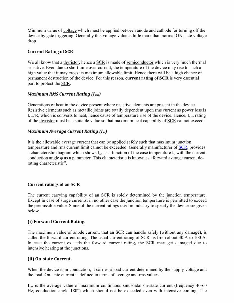
di/dt Protection:
di/dt is the rate of change of current in a device. When SCR is forward biased and is turned ON by the gate signal, the anode current
flows. The anode current requires some time to spread inside the device. (Spreading of charge
carriers) But if the rate of rise of anode current(di/dt) is greater than the spread velocity of charge
carriers then local hot spots is created near the gate due to increased current density. This localised heating may damage the device.
Local spot heating is avoided by ensuring that the conduction spreads to the whole area very rapidly. (OR) The di/dt value must be maintained below a threshold (limiting) value.
This is done by means of connecting an inductor in series with the thyristor.
The inductance L opposes the high di/dt variations. When the current variation is high, the inductor smooths it and protects the SCR from
damage. (Though di/dt variation is high, the inductor ‘L’ smooths it because it takes some time to charge). L ≥ [Vs / (di/dt)]
dv/dt Protection:
dv/dt is the rate of charge of voltage in SCR. We know that iC=C.dv/dt. ie, when dv/dt is high, iC is high. This high current(iC) may turn ON SCR even when gate current is zero. This is called as
dv/dt turn ON or false turn ON of SCR. To protect the thyristor against false turn ON or against high dv/dt a “Snubber Circuit” is
used.
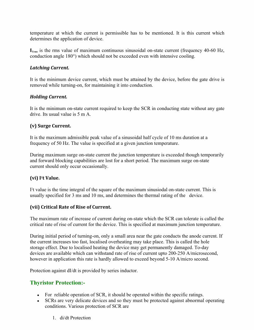
SNUBBER CIRCUIT:
The snubber Circuit is a series combination of resistor ‘R’ and capacitor ‘C’. They are connected across the thyristor to be protected. The capacitor ‘C’ is used to limit the dv/dt across the SCR. The resistor ‘R’ is used to limit high discharging current through the SCR. When switch S is closed, the capacitor ‘C’ behaves as a shortcircuit. Therefore voltage across SCR is zero. As time increases, voltage across ‘C’ increases at a slow rate. Therefore dv/dt across ‘C’ and SCR is less than maximum dv/dt rating of the device. The capacitor charges to full voltage Vs; after which the gate is triggered, and SCR is
turned ON and high current flows through SCR. As di/dt is high, it may damage the SCR.To avoid this, the resistor R in series with ‘C’
will limit the magnitude of di/dt. The technique of ‘snubbing’ can apply to any switching circuit, not only to thyristor/triac
circuits. The rate of rise of turnoff voltage is determined by the time constant
RLC. Where RL is the circuit minimum load resistance, for instance the cold resistance of a heater or lamp, the winding resistance of a motor or the primary resistance of a transformer.
Overvoltage Protection:
Overvoltage may result in false turn ON of the device (or) damage the device. SCR is subjected to internal and external over voltage.
Internal Overvoltage:
The reverse recovery current of the SCR decays at a very fast rate. ie, high di/dt. So a voltage surge is produced whose magnitude is L(di/dt).
External Overvoltage:
These are caused by the interruption of current flow in the inductive circuit and also due to lightning strokes on the lines feeding the SCR systems.
The effect of overvoltage is reduced by using Snubber circuits and NonLinear Resistors called Voltage Clamping Devices.
Voltage Clamping Device:
It is a nonlinear resistor called as VARISTOR (VARIable resiSTOR) connected across the SCR.
The resistance of varistor will decrease with increase in voltage. During normal operation, varistor has high Resistance and draws only small leakage
current. When high voltage appears, it operates in low resistance region and the surge energy is
dissipated across the resistance by producing a virtual shortcircuit across the SCR.
Over Current Protection:
In an SCR due to overcurrent, the junction temperature exceeds the rated value and the device gets damaged.
Overcurrent is interrupted by conventional fuses and circuit breakers. The fault current must be interrupted before the SCR gets damaged and only the faulty
branches of the network should be isolated. Circuit breaker has long tripping time. So it is used for protecting SCR against
continuous over loads (or) against surge currents of long duration. Fast acting current limiting fuse is used to protect SCR against large surge currents of
very short duration.
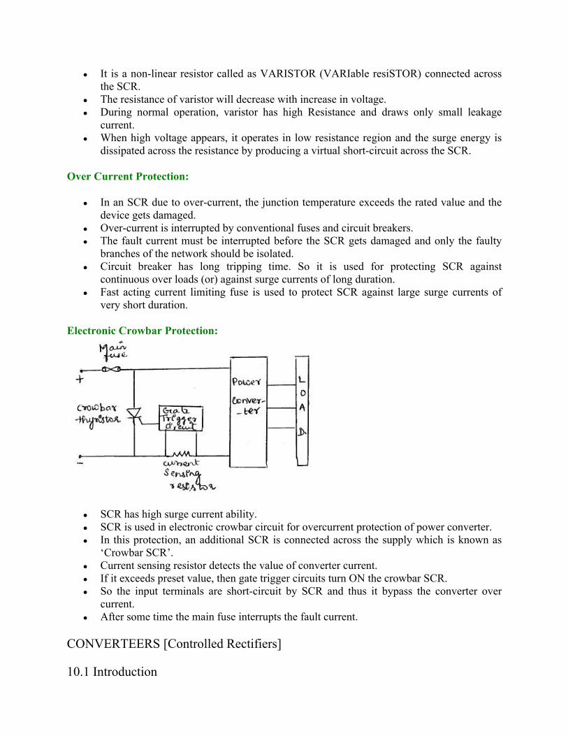
Electronic Crowbar Protection:
SCR has high surge current ability. SCR is used in electronic crowbar circuit for overcurrent protection of power converter. In this protection, an additional SCR is connected across the supply which is known as
‘Crowbar SCR’. Current sensing resistor detects the value of converter current. If it exceeds preset value, then gate trigger circuits turn ON the crowbar SCR. So the input terminals are shortcircuit by SCR and thus it bypass the converter over
current. After some time the main fuse interrupts the fault current.
CONVERTEERS [Controlled Rectifiers]
10.1 Introduction
Single phase uncontrolled rectifiers are extensivel y used in a number of power electronic based converters. In most cases they are used to provide an intermediate unregulated dc voltage source which is further processed to obtain a regulated dc or ac output. They have, in general, been proved to be efficient and robust power stages. However, they suffer from a few disadvantages. The main among them is their inability to control the output dc voltage / current magnitude when the input ac voltage and load parameters remain fixed. They are also unidirectional in the sense that they allow electrical power to flow fromthe ac side to the dc side only. These two disadvantages are the direct consequences of using power diodes inthese converters which can block voltage only in one direction. As will be shown in this module, these two disadvantages are overcome if the diodes are replaced by thyristors, the resulting converters are called fully controlled converters. Thyristors are semicontrolled devices which can be turned ON by applying a current pulse at its gate terminal at a desired instance. However, they cannot be turned off from the gate terminals. Therefore, the fully controlled converter continues to exhibit load dependent output voltage / current waveforms as in the case of their uncontrolled counterpart. However, since the thyristor can block forward voltage, the output voltage / current magnitude can be controlled by controlling the turn on instants of the thyristors. Working principle of thyristors based single phase fully controlled converters will be explained first in the case of a single thyristor halfwave rectifier circuit supplying an R or RL load. However, such converters are rarely used in practice. Full bridge is the most popular configuration used with single phase fully controlled rectifiers.
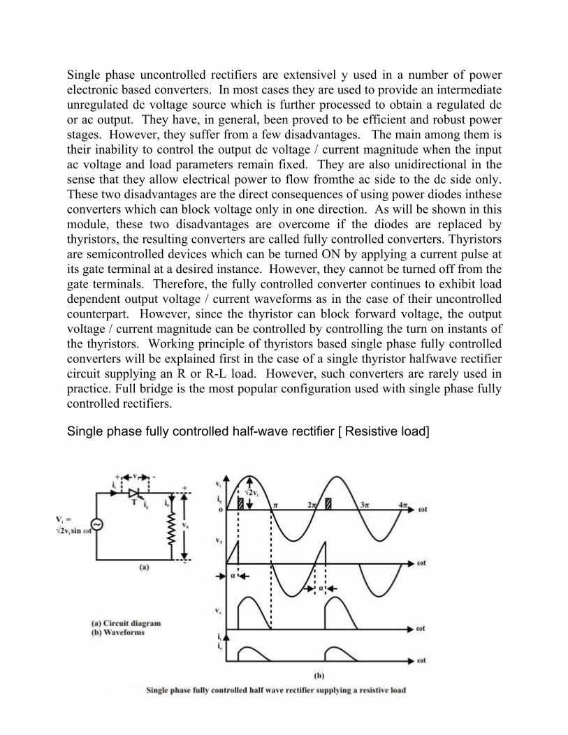
Single phase fully controlled halfwave rectifier [ Resistive load]
The above figure shows the circuit diagram of a single phase fully controlled halfwave rectifier supplying a purely resistive load. At ωt = 0 when the input supply voltage becomes positive the thyristor T becomes forward biased. However, unlike a diode, it does not turn ON till a gate pulse is applied at ω t = α. During the period 0 < ωt ≤ α, the thyristor blocks the supply voltage and the load voltage remains zero as shown in fig 10.1(b). Consequently, no load current flows during this interval. As soon as a gate pulse is applied to the thyristor at ωt = α it turns ON. The voltage across the thyristor collapses to almost zero and the full supply voltage appears across the load. From this point onwards the load voltage follows the supply voltage. The load being purely resistive the load current io is proportional to the load voltage. At ωt = π as the supply voltage passes through the negative going zero crossing the load voltage and hence the load current becomes zero and tries to reverse direction. In the process the thyristor undergoes reverse recovery and starts blocking the negative supply voltage. Therefore, the load voltage and the load current remains clamped at zero till the thyristor is fired again at ωt = 2π + α. The same process repeats there after.
From the discussion above and Fig 10.1 (b) one can write For α < ωt ≤ π
v0= v
i= 2 V sinωt
i
i0 =v0 = 2 Vi sinωtR R
v0 = i0 = 0 otherwise.
1 2 π 1 π
Therefore V =
∫0v dωt =
∫α2 V sinωt dωt
2π 2πOAV 0 i
Or V = Vi (1+ cosα)OAV 2π
1 2π 2V =
∫0v dωt
ORMS 2π
0
1 π 2 2
= ∫α 2vi sin ωtdωt2π
=Vi
2
∫απ (1 cos2ωt)dωt2π
= Vi2 sin2απ α+
2π 2
Vi α sin2α1
=2
1 +π 2π2α
1
+sin2α 2
VORMS
π 1 π 2π∴ FF = =
VOV
OAV
(1+ cosα)
Similar calculation can be done for i0. In particulars for pure resistive loads FFio = FFvo.
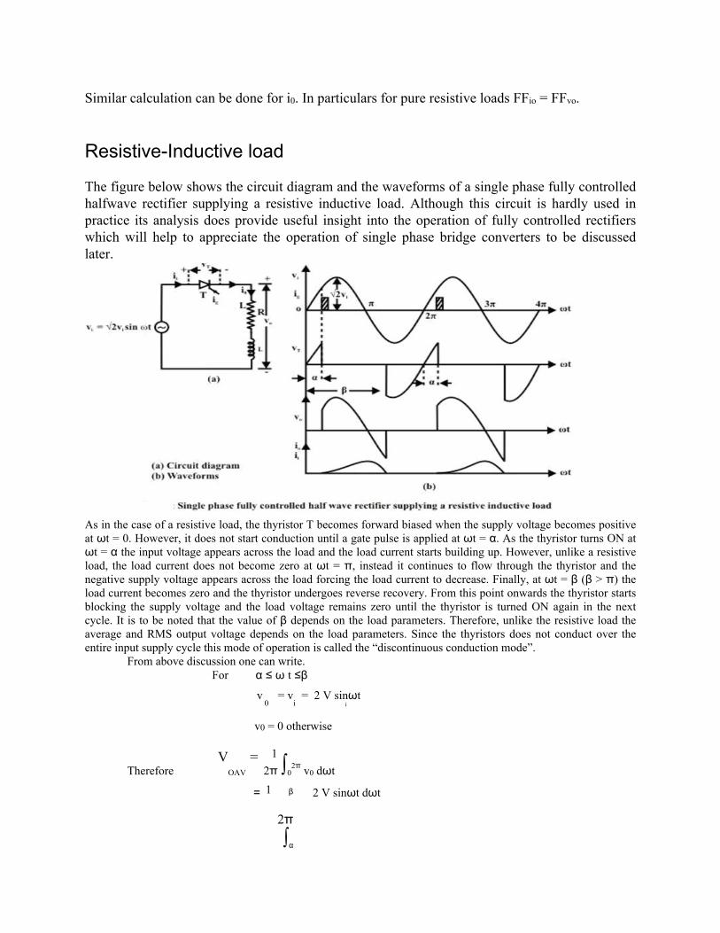
ResistiveInductive load
The figure below shows the circuit diagram and the waveforms of a single phase fully controlled halfwave rectifier supplying a resistive inductive load. Although this circuit is hardly used in practice its analysis does provide useful insight into the operation of fully controlled rectifiers which will help to appreciate the operation of single phase bridge converters to be discussed later.
As in the case of a resistive load, the thyristor T becomes forward biased when the supply voltage becomes positive at ωt = 0. However, it does not start conduction until a gate pulse is applied at ωt = α. As the thyristor turns ON at ωt = α the input voltage appears across the load and the load current starts building up. However, unlike a resistive load, the load current does not become zero at ωt = π, instead it continues to flow through the thyristor and the negative supply voltage appears across the load forcing the load current to decrease. Finally, at ωt = β (β > π) the load current becomes zero and the thyristor undergoes reverse recovery. From this point onwards the thyristor starts blocking the supply voltage and the load voltage remains zero until the thyristor is turned ON again in the next cycle. It is to be noted that the value of β depends on the load parameters. Therefore, unlike the resistive load the average and RMS output voltage depends on the load parameters. Since the thyristors does not conduct over the entire input supply cycle this mode of operation is called the “discontinuous conduction mode”.
From above discussion one can write.For α ≤ ω t ≤β
v0
= vi= 2 V sinωt
i
v0 = 0 otherwise
ThereforeV
OAV
= 1∫02π v0 dωt2π
= 1 β 2 V sinωt dωt
2π ∫α
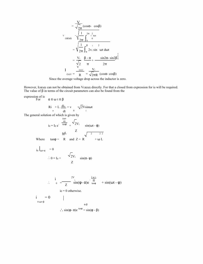
=V
i (cosα cosβ) 2π 1 2π 2
V =
∫0v dωt
ORMS 2π 0
1 β 2 2
= ∫α 2vi sin ωt dωt2π
Vi
1
β α sin2α sin2β= +
2
2 π 2π
I OAV =
VOAV
=Vi
(cosα cosβ)R 2πRSince the average voltage drop across the inductor is zero.
However, IORMS can not be obtained from VORMS directly. For that a closed from expression for i0 will be required. The value of β in terms of the circuit parameters can also be found from the
expression of i0For α ≤ ω t ≤ β
Rio+ L dio = v
0= 2Vsinωt
dt i
The general solution of which is given by
i0 = I0 e
(ωtα)
2Vitanϕ + sin(ωt ϕ)
ωLZ
2 2 2
Where tanφ = R and Z = R + ω L
i0 ωt=α = 0
2Vi∴ 0 = I0 + sin(α φ)Z
∴i0 =
2Vi
( ω tα)
sin(φ α)e tanφ + sin(ωt φ)Z
i0 = 0 otherwise.
i 0 ωt=β
= 0αβ
∴ sin(φ α)e tanφ = sin(φ β)
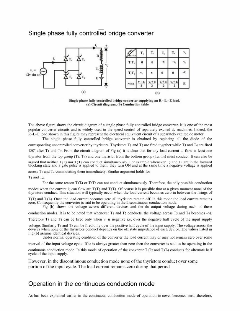
Single phase fully controlled bridge converter
The above figure shows the circuit diagram of a single phase fully controlled bridge converter. It is one of the most popular converter circuits and is widely used in the speed control of separately excited dc machines. Indeed, the R–L–E load shown in this figure may represent the electrical equivalent circuit of a separately excited dc motor.
The single phase fully controlled bridge converter is obtained by replacing all the diode of the corresponding uncontrolled converter by thyristors. Thyristors T1 and T2 are fired together while T3 and T4 are fired 180º after T1 and T2. From the circuit diagram of Fig (a) it is clear that for any load current to flow at least one thyristor from the top group (T1, T3) and one thyristor from the bottom group (T2, T4) must conduct. It can also be argued that neither T1T3 nor T2T4 can conduct simultaneously. For example whenever T3 and T4 are in the forward blocking state and a gate pulse is applied to them, they turn ON and at the same time a negative voltage is applied across T1 and T2 commutating them immediately. Similar argument holds forT1 and T2.
For the same reason T1T4 or T2T3 can not conduct simultaneously. Therefore, the only possible conduction modes when the current i0 can flow are T1T2 and T3T4. Of coarse it is possible that at a given moment none of the thyristors conduct. This situation will typically occur when the load current becomes zero in between the firings of T1T2 and T3T4. Once the load current becomes zero all thyristors remain off. In this mode the load current remains zero. Consequently the converter is said to be operating in the discontinuous conduction mode.
Fig (b) shows the voltage across different devices and the dc output voltage during each of these
conduction modes. It is to be noted that whenever T1 and T2 conducts, the voltage across T3 and T4 becomes –vi. Therefore T3 and T4 can be fired only when vi is negative i.e, over the negative half cycle of the input supply voltage. Similarly T1 and T2 can be fired only over the positive half cycle of the input supply. The voltage across the devices when none of the thyristors conduct depends on the off state impedance of each device. The values listed in Fig (b) assume identical devices.
Under normal operating condition of the converter the load current may or may not remain zero over some
interval of the input voltage cycle. If i0 is always greater than zero then the converter is said to be operating in the continuous conduction mode. In this mode of operation of the converter T1T2 and T3T4 conducts for alternate half cycle of the input supply.
However, in the discontinuous conduction mode none of the thyristors conduct over some portion of the input cycle. The load current remains zero during that period
Operation in the continuous conduction mode
As has been explained earlier in the continuous conduction mode of operation i0 never becomes zero, therefore,
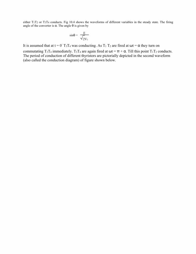
either T1T2 or T3T4 conducts. Fig 10.4 shows the waveforms of different variables in the steady state. The firing angle of the converter is α. The angle θ is given by
sinθ = E
2V1
It is assumed that at t = 0 T3T4 was conducting. As T1 T2 are fired at ωt = α they turn on commutating T3T4 immediately. T3T4 are again fired at ωt = π + α. Till this point T1T2 conducts. The period of conduction of different thyristors are pictorially depicted in the second waveform (also called the conduction diagram) of figure shown below.
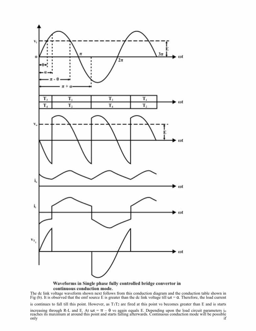
The dc link voltage waveform shown next follows from this conduction diagram and the conduction table shown in Fig (b). It is observed that the emf source E is greater than the dc link voltage till ωt = α. Therefore, the load current i0 continues to fall till this point. However, as T1T2 are fired at this point v0 becomes greater than E and i0 starts increasing through RL and E. At ωt = π – θ v0 again equals E. Depending upon the load circuit parameters io reaches its maximum at around this point and starts falling afterwards. Continuous conduction mode will be possible only if
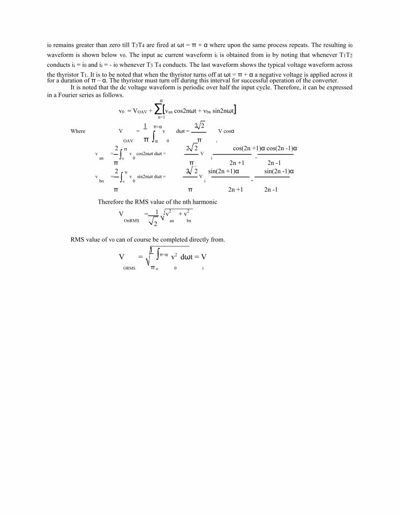
i0 remains greater than zero till T3T4 are fired at ωt = π + α where upon the same process repeats. The resulting i0 waveform is shown below v0. The input ac current waveform ii is obtained from i0 by noting that whenever T1T2 conducts ii = i0 and ii = i0 whenever T3 T4 conducts. The last waveform shows the typical voltage waveform across the thyristor T1. It is to be noted that when the thyristor turns off at ωt = π + α a negative voltage is applied across it for a duration of π – α. The thyristor must turn off during this interval for successful operation of the converter.
It is noted that the dc voltage waveform is periodic over half the input cycle. Therefore, it can be expressed in a Fourier series as follows.
α
v0 = VOAV + ∑[van cos2nωt + vbn sin2nωt]n=1
1 π+α 2 2Where V =
π ∫αv dωt = V cosα
πOAV 0 i
2 π 2 2 cos(2n +1)α cos(2n 1)αv = ∫0 v cos2nωt dωt = Van 0
π πi
2n +1 2n 12 π 2 2 sin(2n +1)α sin(2n 1)α
v = ∫0 v sin2nωt dωt = V bn 0
π πi
2n +1 2n 1
Therefore the RMS value of the nth harmonic
V = 1 v2 + v2OnRMS 2 an bn
RMS value of v0 can of course be completed directly from.
V = 1 ∫π+α v2 dωt = VORMS π α 0 i
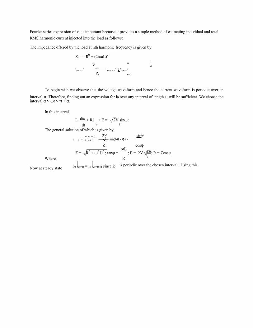
Fourier series expression of v0 is important because it provides a simple method of estimating individual and total RMS harmonic current injected into the load as follows:
The impedance offered by the load at nth harmonic frequency is given by
Zn = R2 + (2nωL)2
V α 12
IonRMS
= onRMS ; IOHRMS
= ∑I
onRMS2
Zn n=1
To begin with we observe that the voltage waveform and hence the current waveform is periodic over an
interval π. Therefore, finding out an expression for i0 over any interval of length π will be sufficient. We choose the interval α ≤ ωt ≤ π + α.
In this interval
L di0 + Ri0
+ E = 2V sinωtdt i
The general solution of which is given by
Where,
Now at steady state
( ω tα) 2V sinθi 0 = Ie tanφ +
i sin(ωt φ)
Z cosφ
Z = R2 + ω2 L2 ; tanφ =ωL
; E = 2V sinθ; R = ZcosφR i
i0 = i0ωt=α ωt=π+α since i0 is periodic over the chosen interval. Using this
boundary condition we obtain
2V 2sin(φ α) ( ωtα)tanφ
i0
= iπ e + sin(ωt φ)
Z tanφ
1 e
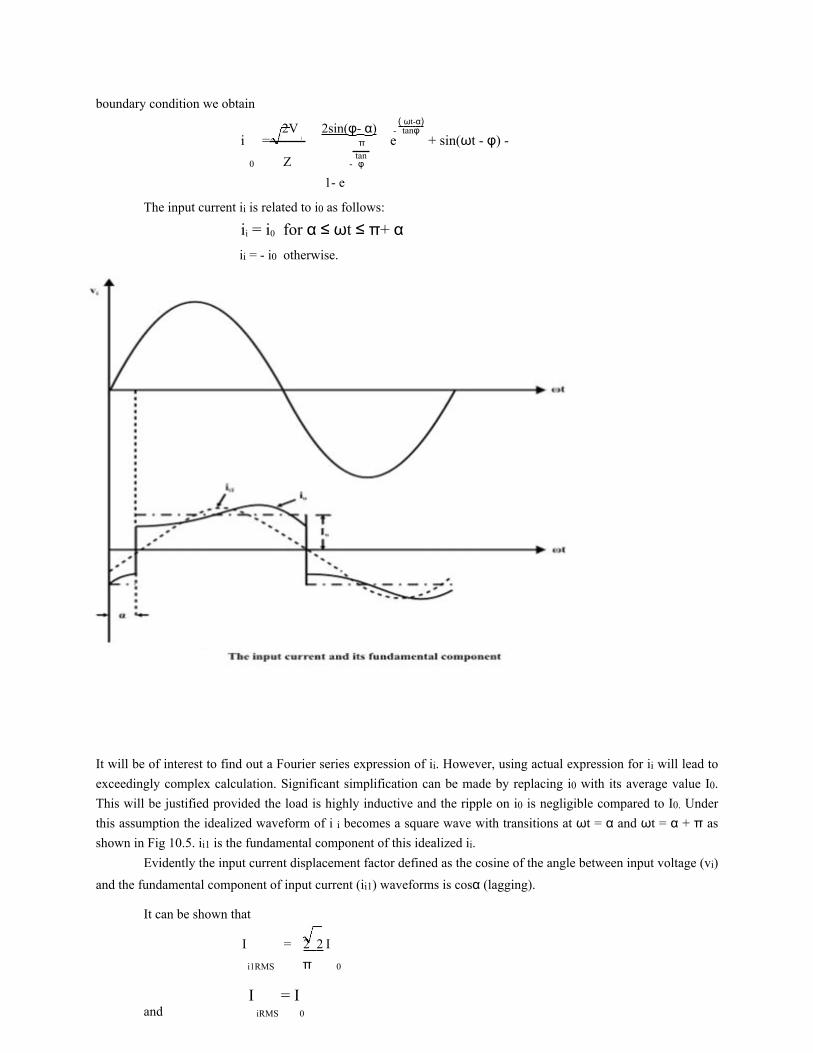
The input current ii is related to i0 as follows:
ii = i0 for α ≤ ωt ≤ π+ αii = i0 otherwise.
It will be of interest to find out a Fourier series expression of ii. However, using actual expression for ii will lead to exceedingly complex calculation. Significant simplification can be made by replacing i0 with its average value I0. This will be justified provided the load is highly inductive and the ripple on i0 is negligible compared to I0. Under this assumption the idealized waveform of i i becomes a square wave with transitions at ωt = α and ωt = α + π as shown in Fig 10.5. ii1 is the fundamental component of this idealized ii.
Evidently the input current displacement factor defined as the cosine of the angle between input voltage (vi) and the fundamental component of input current (ii1) waveforms is cosα (lagging).
It can be shown that
Ii1RMS
= 2 2 I0π
andI iRMS
= I0
Therefore the input current distortion factor =Ii1RMS = 2 2IiRMS π
The input power factor =Actual Power
=Vi Ii1RMS cosα
Apparent Power V IiRMSi
=2 2
cosα (lagging)π
Therefore, the rectifier appears as a lagging power factor load to the input ac system. Larger the ‘α’ poorer is the power factor.
The input current ii also contain significant amount of harmonic current (3rd, 5th, etc) and therefore appears
as a harmonic source to the utility. Exact composition of the harmonic currents can be obtained by Fourier series
analysis of ii and is left as an exercise.Operation in the discontinuous conduction mode
So far we have assumed that the converter operates in continuous conduction mode without paying attention to the load condition required for it. In figure 10.4 the voltage across the R and L component of the load is negative in the
region π θ ≤ ωt ≤ π + α. Therefore i0 continues to decrease till a new pair of thyristor is fired at ωt = π + α. Now if the value of R, L and E are such that i0 becomes zero before ωt = π + α the conduction becomes discontinuous. Obviously then, at the boundary between continuous and discontinuous conduction the minimum value of i0 which occurs at ωt = α and ωt = π + α will be zero. Putting this condition in (10.26) we obtain the condition for continuous conduction as.
2sin(φ α) sin(φ α) sinθ ≥ 0 π cosφtanφ1 e
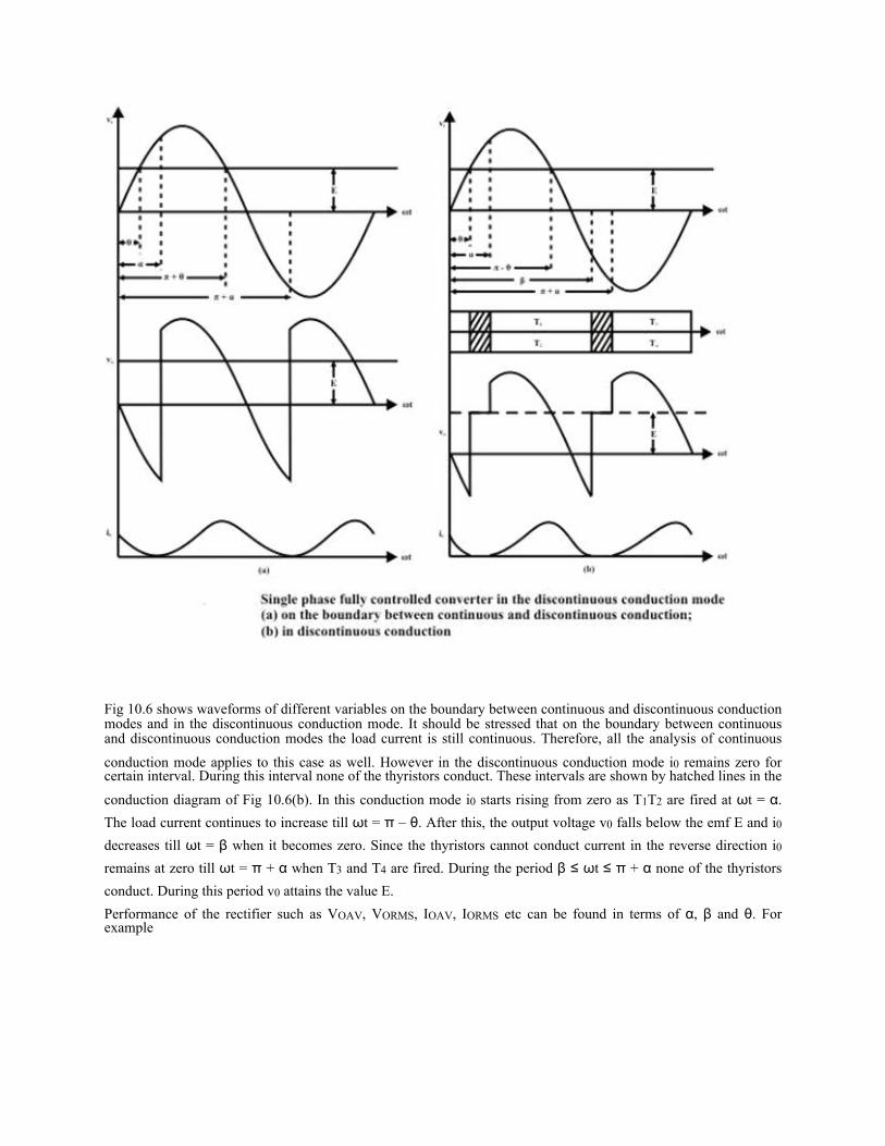
Fig 10.6 shows waveforms of different variables on the boundary between continuous and discontinuous conduction modes and in the discontinuous conduction mode. It should be stressed that on the boundary between continuous and discontinuous conduction modes the load current is still continuous. Therefore, all the analysis of continuous
conduction mode applies to this case as well. However in the discontinuous conduction mode i0 remains zero for certain interval. During this interval none of the thyristors conduct. These intervals are shown by hatched lines in the
conduction diagram of Fig 10.6(b). In this conduction mode i0 starts rising from zero as T1T2 are fired at ωt = α. The load current continues to increase till ωt = π – θ. After this, the output voltage v0 falls below the emf E and i0 decreases till ωt = β when it becomes zero. Since the thyristors cannot conduct current in the reverse direction i0 remains at zero till ωt = π + α when T3 and T4 are fired. During the period β ≤ ωt ≤ π + α none of the thyristors conduct. During this period v0 attains the value E.Performance of the rectifier such as VOAV, VORMS, IOAV, IORMS etc can be found in terms of α, β and θ. For example
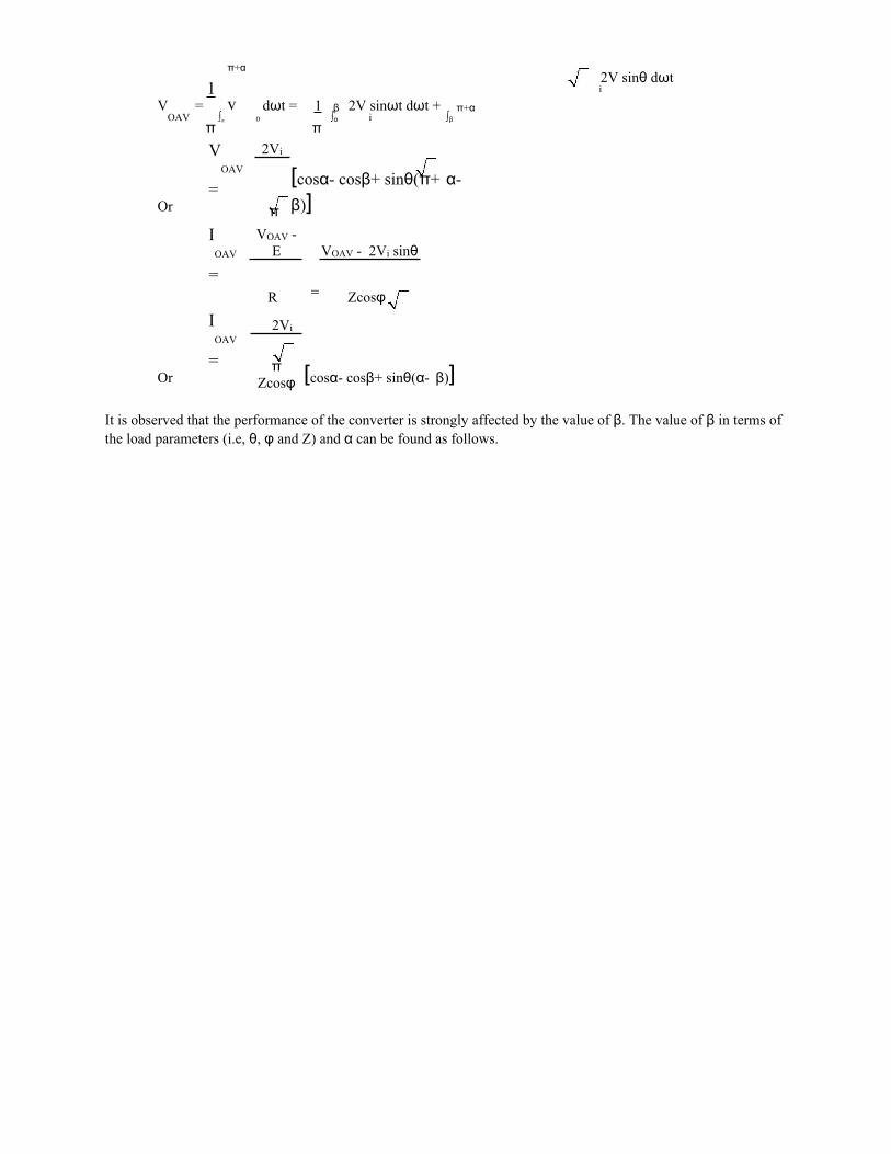
V = 1
π+α
v0dωt = 1 β 2V sinωt dωt + π+α
OAVπ
∫α ∫α i ∫βπ
Or
VOAV
=
2Vi
[cosα cosβ+ sinθ(π+ α β)]π
IOAV
=
VOAV E
=
VOAV 2Vi sinθ
R Zcosφ
Or
IOAV
=
2Vi
[cosα cosβ+ sinθ(α β)]π Zcosφ
2V sinθ dωti
It is observed that the performance of the converter is strongly affected by the value of β. The value of β in terms of the load parameters (i.e, θ, φ and Z) and α can be found as follows.
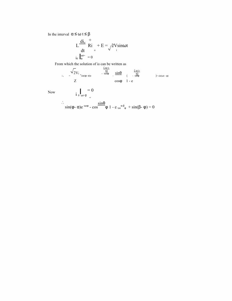
In the interval α ≤ ω t ≤ β
Ldio +
Rio+ E = 2Vsinωt
dt i
i0ωt=α = 0
From which the solution of i0 can be written as
2Vi
( ω tα)
sinθ( ω tα)tanφ
i 0 =
Zsin(φ α)e
cosφ tanφ + sin(ωt φ)
1 e
Now i 0 ωt=β
= 0αβ
∴ sin(φ α)e tanφ cos
sinθφ 1 e tanαβφ + sin(β φ) = 0