computational electronics. a.1 derivation of the boltzmann transport equation kinetic theory: we...
TRANSCRIPT
Computational Electronics
Computational Electronics
Computational Electronics
tftAddtA ,,,, rvrvvr
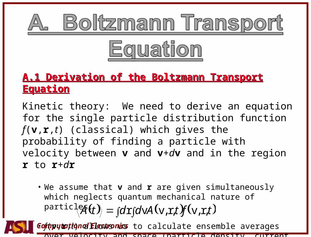
A.1 Derivation of the Boltzmann Transport EquationA.1 Derivation of the Boltzmann Transport Equation
Kinetic theory: We need to derive an equation for the single particle distribution function f(v,r,t) (classical) which gives the probability of finding a particle with velocity between v and v+dv and in the region r to r+dr
• We assume that v and r are given simultaneously which neglects quantum mechanical nature of particles.
• f(v,r,t) allows us to calculate ensemble averages over velocity and space (particle density, current density, energy density, etc.):
Computational Electronics
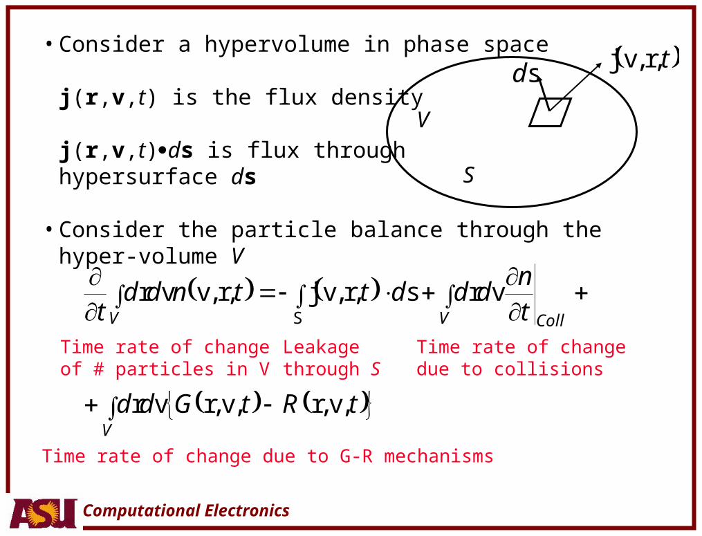
• Consider a hypervolume in phase space
j(r,v,t) is the flux density
j(r,v,t)ds is flux through hypersurface ds
• Consider the particle balance through the hyper-volume V
CollVV tn
dddttnddt
vrsrvjrvvrS
,,,,
Time rate of changeof # particles in V
Leakage through S
Time rate of changedue to collisions
tRtGddV
,,,, vrvrvr
Time rate of change due to G-R mechanisms
V
S
t,,rvjsd
Computational Electronics
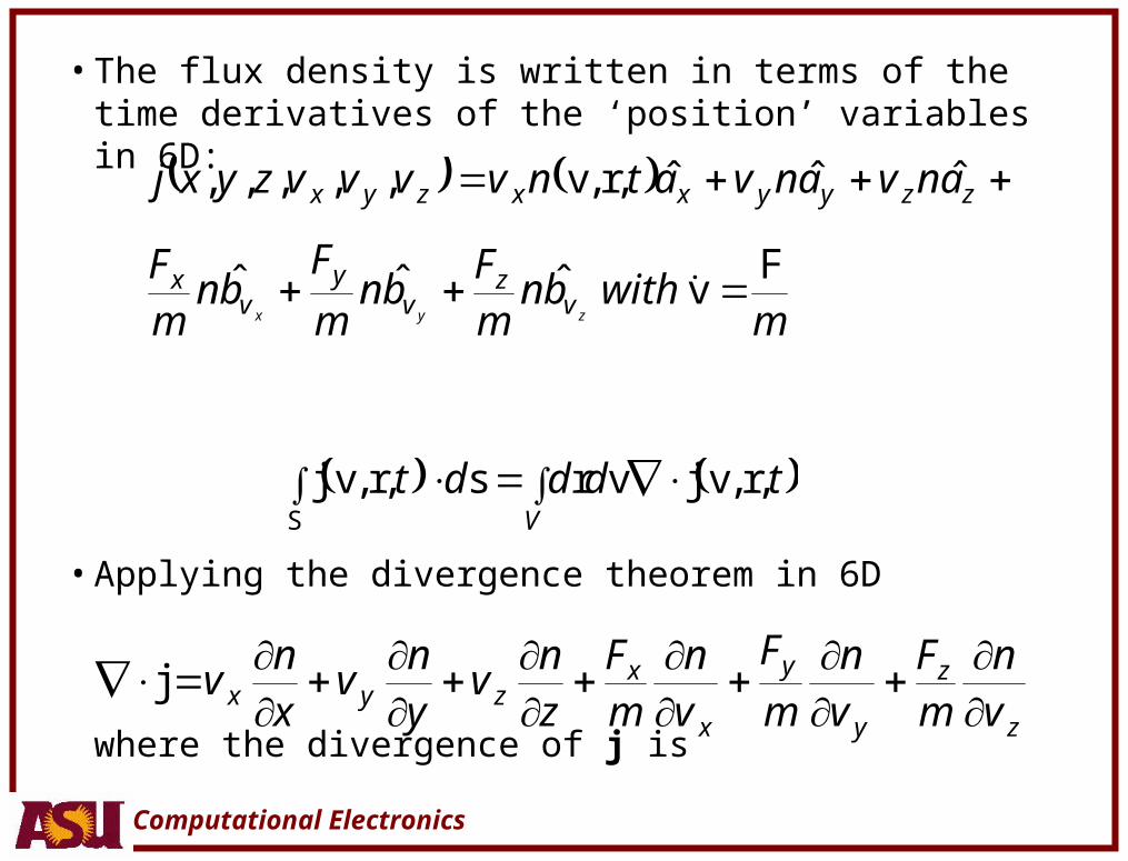
• The flux density is written in terms of the time derivatives of the ‘position’ variables in 6D:
• Applying the divergence theorem in 6D
where the divergence of j is
mwithbn
mF
bnm
Fbn
mF
anvanvatnvvvvzyxj
zyx vz
vy
vx
zzyyxxzyx
Fv
rv
ˆˆˆ
ˆˆˆ,,,,,,,
V
tdddt ,,,, rvjvrsrvjS
z
z
y
y
x
xzyx v
nmF
vn
m
F
vn
mF
zn
vyn
vxn
v
j
Computational Electronics
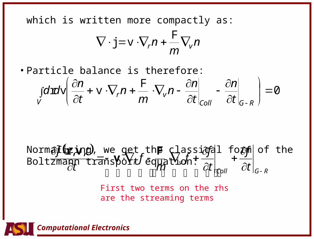
which is written more compactly as:
• Particle balance is therefore:
Normalizing, we get the classical form of the Boltzmann transport equation:
nm
n vr Fvj
0F
vvr
RGColl
vrV t
ntn
nm
ntn
dd
RGColl
vr t
f
t
ff
mf
t
tf
Fv
vr ,,
First two terms on the rhs are the streaming terms
Computational Electronics
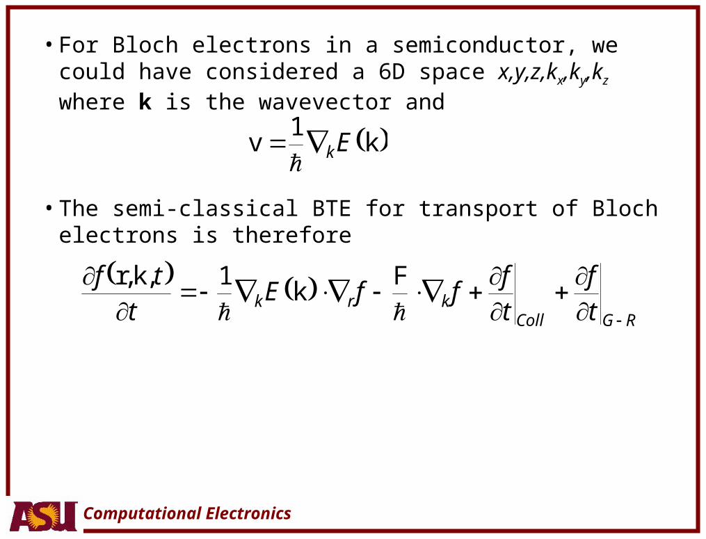
• For Bloch electrons in a semiconductor, we could have considered a 6D space x,y,z,kx,ky,kz where k is the wavevector and
• The semi-classical BTE for transport of Bloch electrons is therefore
k1
v Ek
RGColl
krk tf
tf
ffEt
tf
F
k1kr ,,
Computational Electronics
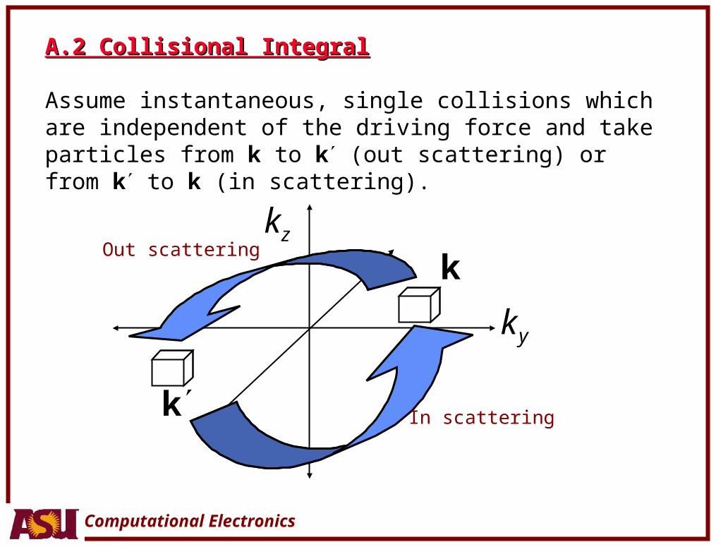
A.2 Collisional IntegralA.2 Collisional Integral
Assume instantaneous, single collisions which are independent of the driving force and take particles from k to k (out scattering) or from k to k (in scattering).
k
kzk
yk
xkIn scattering
Out scattering
Computational Electronics
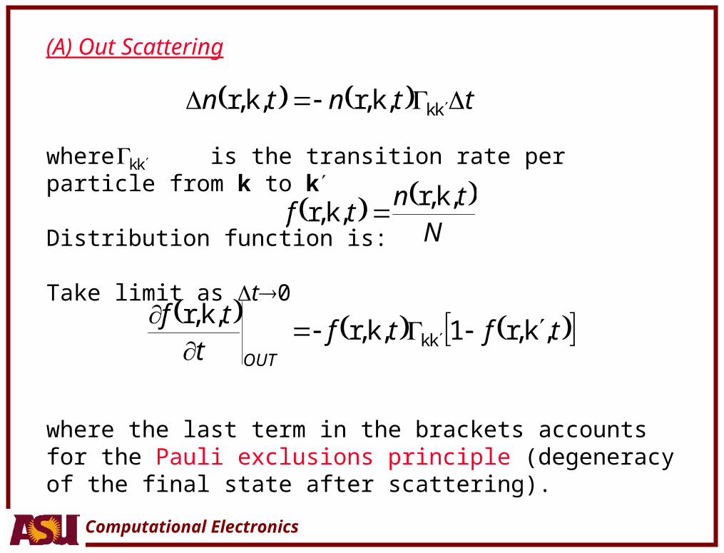
(A) Out Scattering
where is the transition rate per particle from k to k
Distribution function is:
Take limit as t0
where the last term in the brackets accounts for the Pauli exclusions principle (degeneracy of the final state after scattering).
ttntn kkkrkr ,,,,
kk
N
tntf
,,,,
krkr
tftft
tf
OUT
,,,,,,
kr1krkr
kk
Computational Electronics
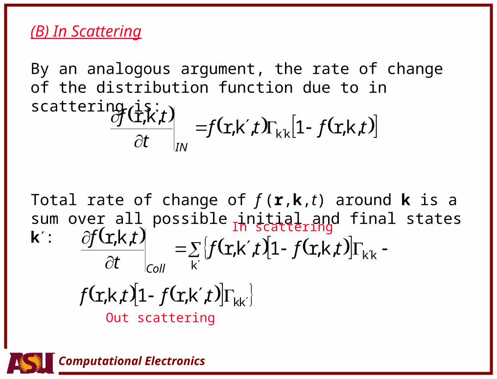
(B) In Scattering
By an analogous argument, the rate of change of the distribution function due to in scattering is:
Total rate of change of f (r,k,t) around k is a sum over all possible initial and final states k:
tftft
tf
IN
,,,,,,
kr1krkr
kk
kk
kkk
kr1kr
kr1krkr
tftf
tftft
tf
Coll
,,,,
,,,,,,
In scattering
Out scattering
Computational Electronics
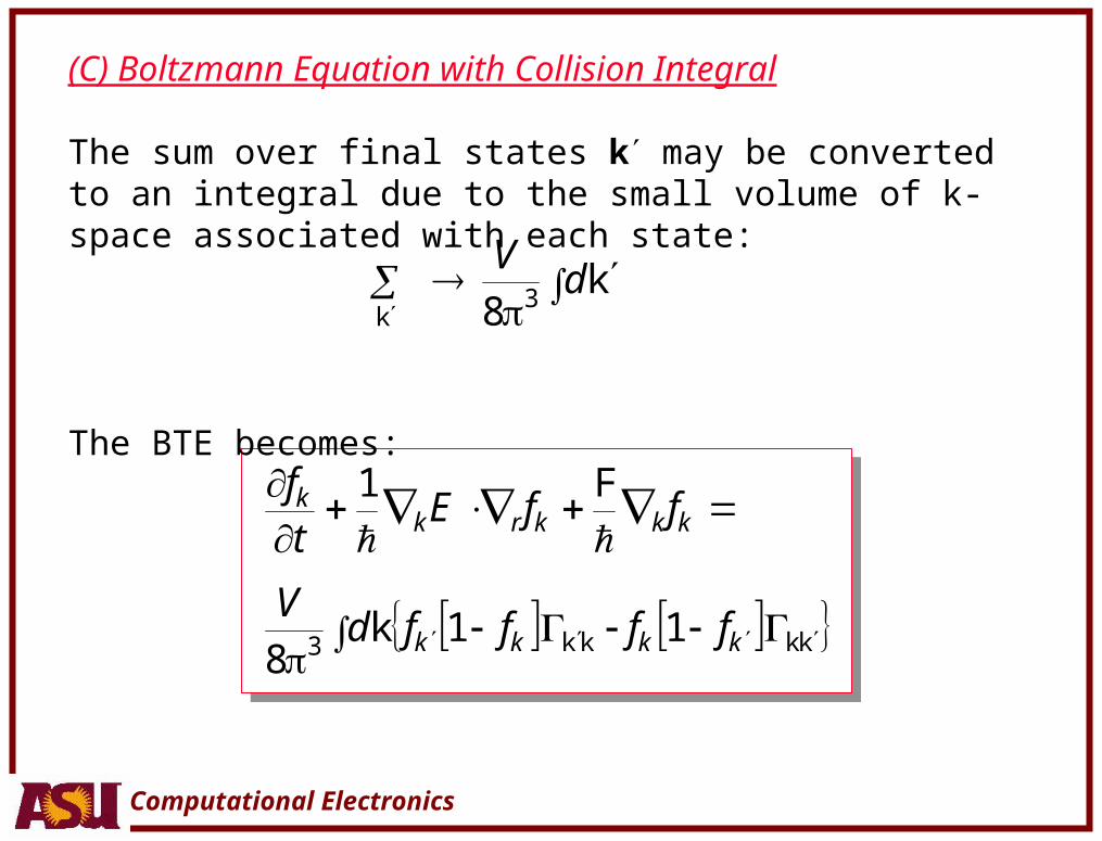
(C) Boltzmann Equation with Collision Integral
The sum over final states k may be converted to an integral due to the small volume of k-space associated with each state:
The BTE becomes:
kkkk3 11k8
F1
kkkk
kkkrkk
ffffdV
ffEtf
k8 3
kd
V
Computational Electronics
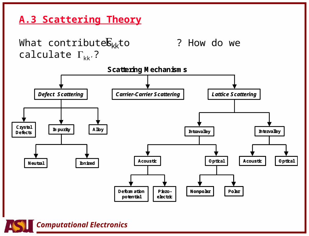
A.3 Scattering Theory
What contributes to ? How do we calculate kk’?kk
Scattering Mechanisms
Defect Scattering Carrier-Carrier Scattering Lattice Scattering
CrystalDefects
Impurity Alloy
Neutral Ionized
Intravalley Intervalley
Acoustic OpticalAcoustic Optical
Nonpolar PolarDeformationpotential
Piezo-electric
Scattering Mechanisms
Defect Scattering Carrier-Carrier Scattering Lattice Scattering
CrystalDefects
Impurity Alloy
Neutral Ionized
Intravalley Intervalley
Acoustic OpticalAcoustic OpticalAcoustic Optical
Nonpolar PolarNonpolar PolarDeformationpotential
Piezo-electric
Computational Electronics
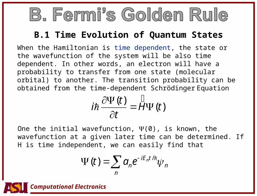
B.1 Time Evolution of Quantum States
When the Hamiltonian is time dependent, the state or the wavefunction of the system will be also time dependent. In other words, an electron will have a probability to transfer from one state (molecular orbital) to another. The transition probability can be obtained from the time-dependent Schrödinger Equation
)()(
tHt
ti
One the initial wavefunction, (0), is known, the wavefunction at a given later time can be determined. If H is time independent, we can easily find that
nn
tiEn
neat /)(
Computational Electronics
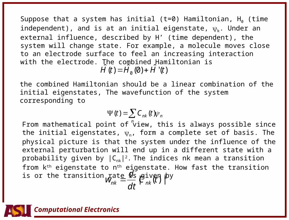
Suppose that a system has initial (t=0) Hamiltonian, H0 (time independent), and is at an initial eigenstate, k. Under an external influence, described by H’ (time dependent), the system will change state. For example, a molecule moves close to an electrode surface to feel an increasing interaction with the electrode. The combined Hamiltonian is
)('ˆ)0(ˆ)(ˆ0 tHHtH
the combined Hamiltonian should be a linear combination of the initial eigenstates, The wavefunction of the system corresponding to
nn
nk tCt )()(
From mathematical point of view, this is always possible since the initial eigenstates, n, form a complete set of basis. The physical picture is that the system under the influence of the external perturbation will end up in a different state with a probability given by |Cnk|2. The indices nk mean a transition from kth eigenstate to nth eigenstate. How fast the transition is or the transition rate is given by
2|)(| tCdt
dw nknk
Computational Electronics
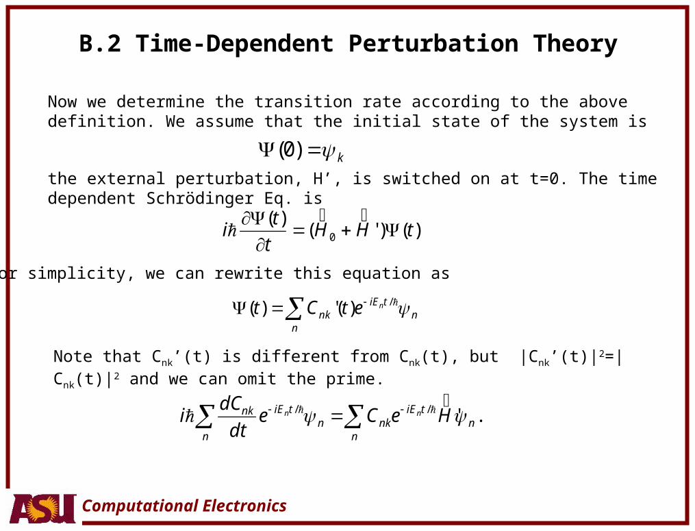
B.2 Time-Dependent Perturbation Theory
Now we determine the transition rate according to the above definition. We assume that the initial state of the system is
k )0(the external perturbation, H’, is switched on at t=0. The time dependent Schrödinger Eq. is
)()'()(
0 tHHt
ti
For simplicity, we can rewrite this equation as
ntiE
nnk
netCt /)(')(
Note that Cnk’(t) is different from Cnk(t), but |Cnk’(t)|2=| Cnk(t)|2 and we can omit the prime.
.'//n
n
tiEnkn
n
tiEnk HeCedt
dCi nn
Computational Electronics
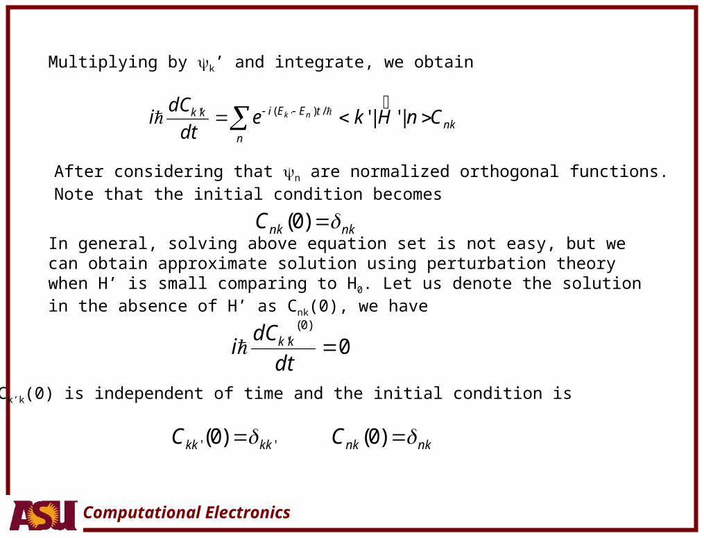
Multiplying by k’ and integrate, we obtain
nkn
tEEikk CnHkedt
dCi nk |'|'/)(' '
After considering that n are normalized orthogonal functions. Note that the initial condition becomes
0)0(
' dt
dCi kk
nknkC )0(
In general, solving above equation set is not easy, but we can obtain approximate solution using perturbation theory when H’ is small comparing to H0. Let us denote the solution in the absence of H’ as Cnk(0), we have
So Ck’k(0) is independent of time and the initial condition is
'' )0( kkkkC nknkC )0(
Computational Electronics
kHkedt
dCi tEEikk kk |'|'/)(
)1(' '
kHk |'|'
,1 /)(
0
'''
' dteHi
C tEEit
kkkkkk
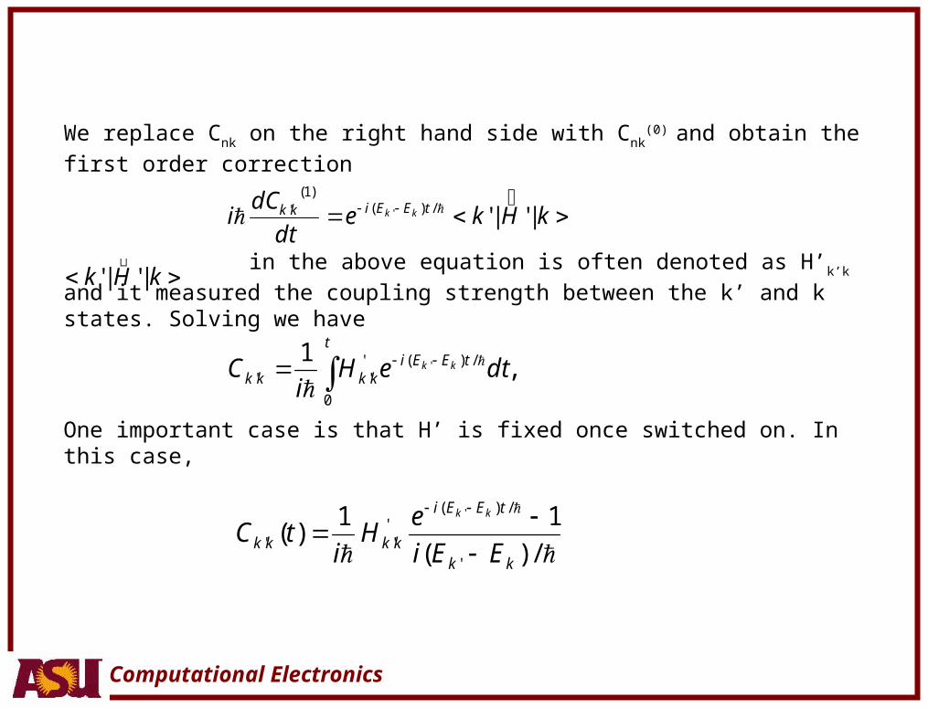
We replace Cnk on the right hand side with Cnk(0)
and obtain the first order correction
in the above equation is often denoted as H’k’k and it measured the
coupling strength between the k’ and k states. Solving we have
One important case is that H’ is fixed once switched on. In this case,
/)(
11)(
'
/)('''
'
kk
tEEi
kkkk EEi
eH
itC
kk
Computational Electronics
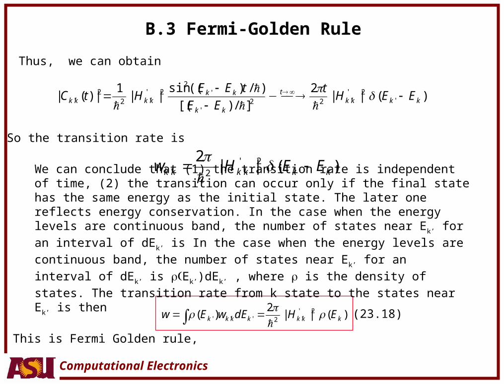
B.3 Fermi-Golden Rule
)(||2
]/)[(
)/)((sin||
1|)(| '
2''22
'
'2
2''2
2' kkkk
t
kk
kkkkkk EEH
t
EE
tEEHtC
)(||2
'2'
'2' kkkkkk EEHw
Thus, we can obtain
So the transition rate is
We can conclude that (1) the transition rate is independent of time, (2) the transition can occur only if the final state has the same energy as the initial state. The later one reflects energy conservation. In the case when the energy levels are continuous band, the number of states near Ek’ for an interval of dEk’ is In the case
when the energy levels are continuous band, the number of states near Ek’ for an
interval of dEk’ is Ek’)dEk’ , where is the density of states. The transition rate
from k state to the states near Ek’ is then
)(||2
)( 2''2''' kkkkkkk EHdEwEw
This is Fermi Golden rule,
(23.18)
Computational Electronics
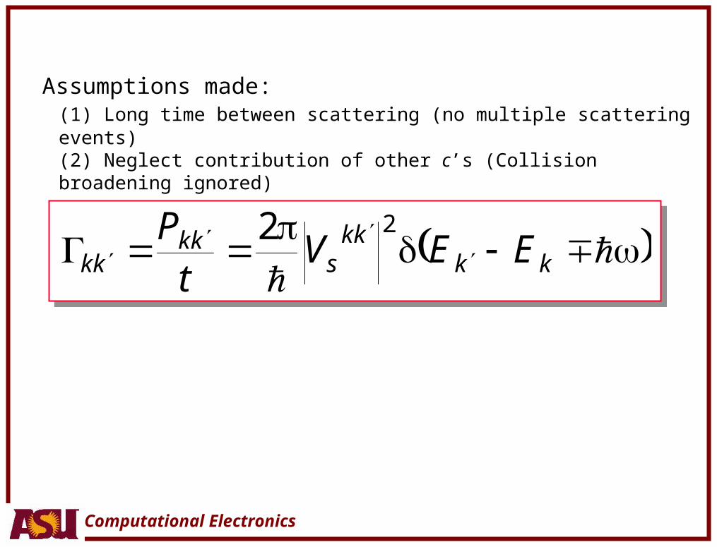
Assumptions made: (1) Long time between scattering (no multiple scattering events)(2) Neglect contribution of other c’s (Collision broadening ignored)
kk
kks
kkkk EEV
tP 22
Computational Electronics
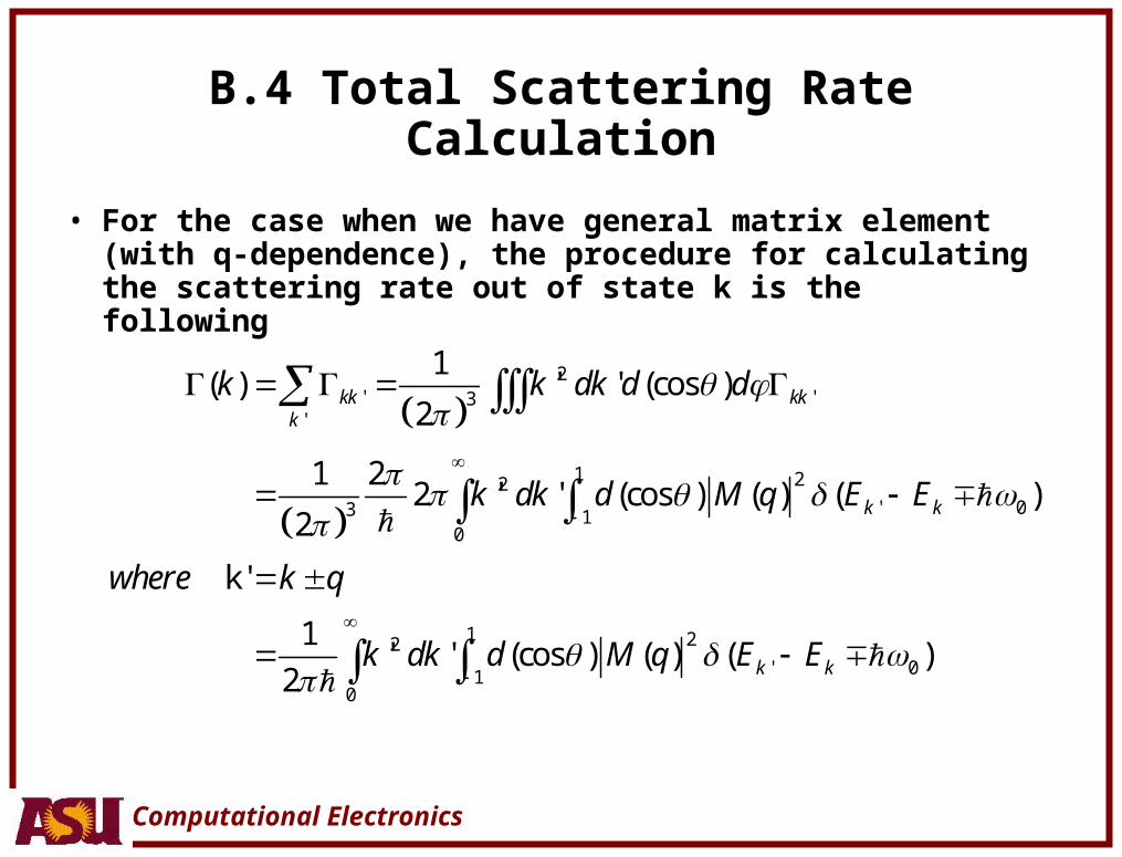
B.4 Total Scattering Rate Calculation
• For the case when we have general matrix element (with q-dependence), the procedure for calculating the scattering rate out of state k is the following
2' '3
'
1 22' 03 1
0
1 22' 01
0
1( ) ' ' (cos )
2
1 22 ' ' (cos ) ( ) ( )
2
k'
1' ' (cos ) ( ) ( )
2
kk kkk
k k
k k
k k dk d d
k dk d M q E E
where k q
k dk d M q E E
Computational Electronics
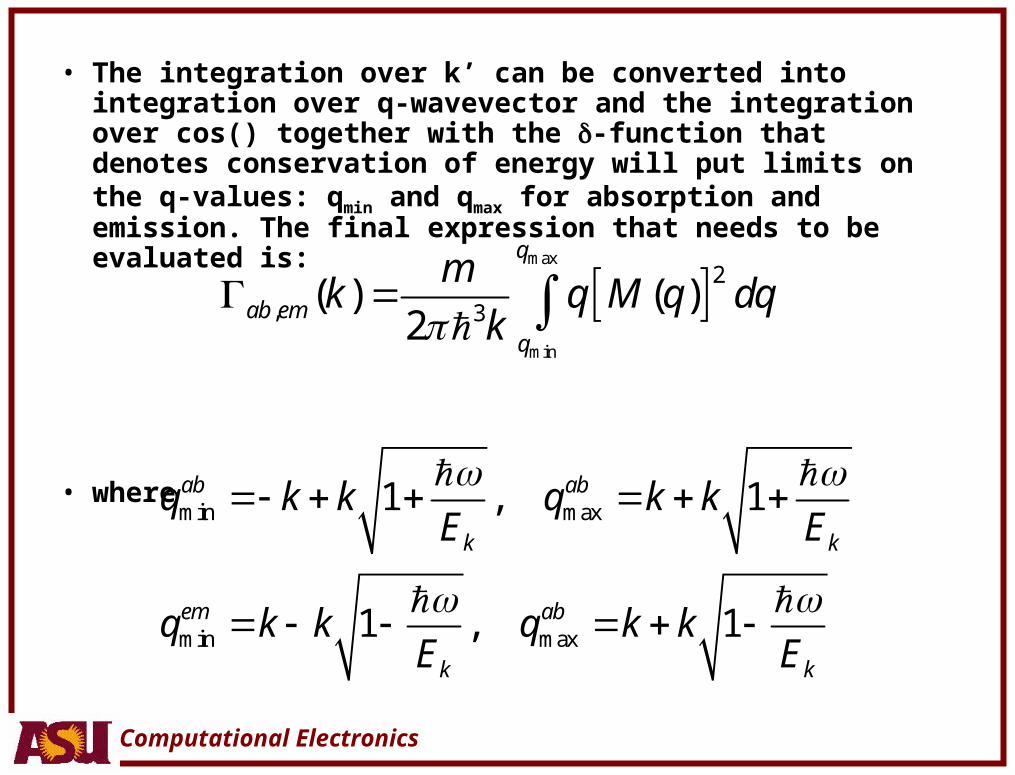
• The integration over k’ can be converted into integration over q-wavevector and the integration over cos() together with the -function that denotes conservation of energy will put limits on the q-values: qmin and qmax for absorption and emission. The final expression that needs to be evaluated is:
• where
max
min
2
, 3( ) ( )
2
q
ab em
q
mk q M q dq
k
min max
min max
1 , 1
1 , 1
ab ab
k k
em ab
k k
q k k q k kE E
q k k q k kE E
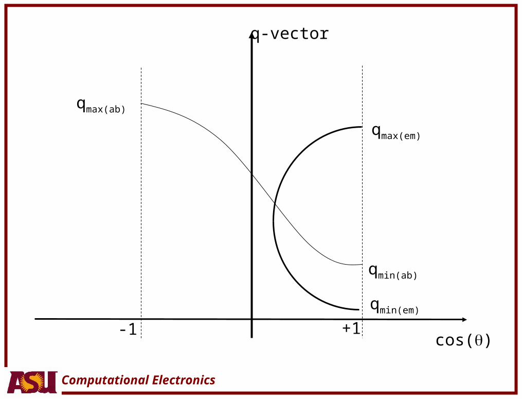
Computational Electronics
qmin(em)
qmax(ab)
qmin(ab)
q-vector
cos()-1 +1
qmax(em)
Computational Electronics
0 0.5 1 1.5 2 2.5 3 3.50
0.5
1
1.5
2
2.5
3
3.5x 10
5
polar angle
Emission Process
0 0.5 1 1.5 2 2.5 3 3.50
0.5
1
1.5
2
2.5
3
3.5x 10
5
polar angle
Absorption Process
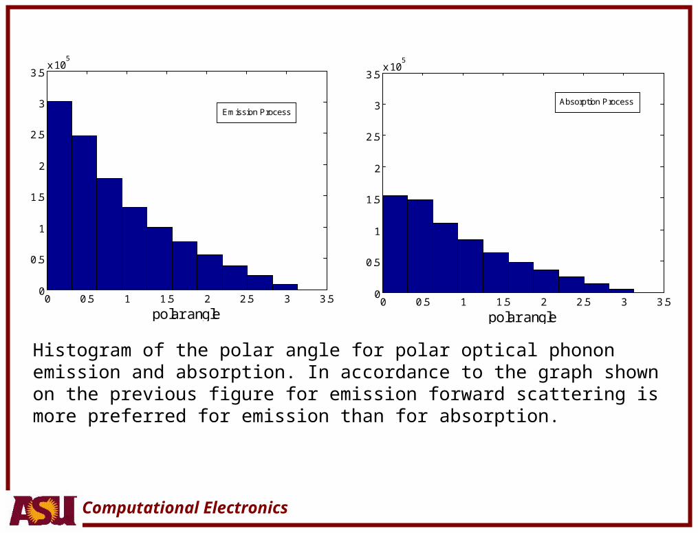
Histogram of the polar angle for polar optical phonon emission and absorption. In accordance to the graph shown on the previous figure for emission forward scattering is more preferred for emission than for absorption.
Computational Electronics
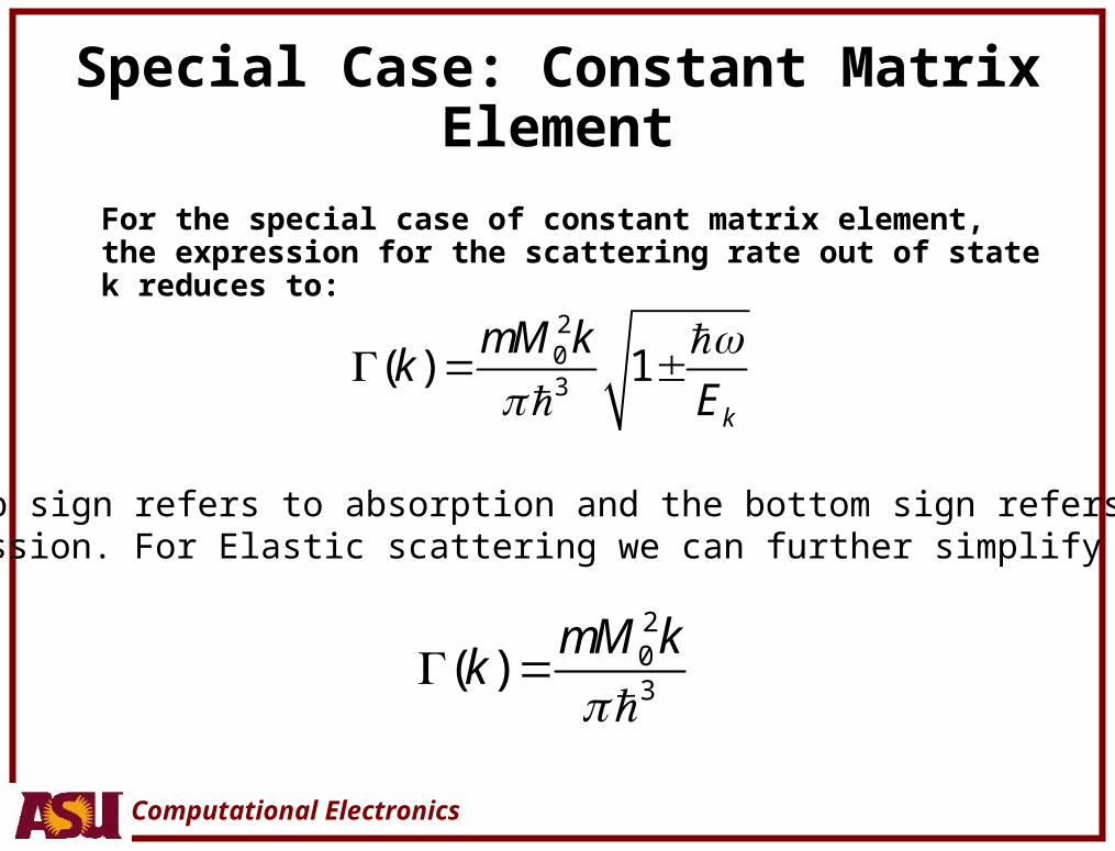
Special Case: Constant Matrix Element
For the special case of constant matrix element, the expression for the scattering rate out of state k reduces to:
203
( ) 1k
mM kk
E
The top sign refers to absorption and the bottom sign refersTo emission. For Elastic scattering we can further simplify to get:
203
( )mM k
k
Computational Electronics
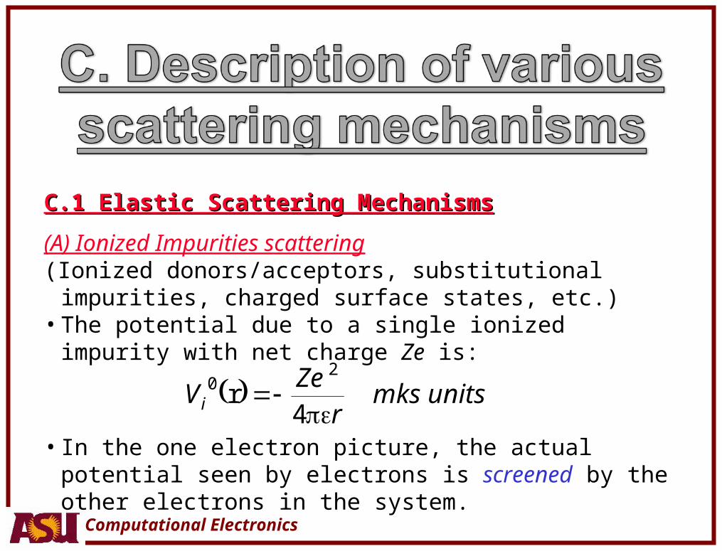
C.1 Elastic Scattering MechanismsC.1 Elastic Scattering Mechanisms
(A) Ionized Impurities scattering (Ionized donors/acceptors, substitutional impurities, charged
surface states, etc.)• The potential due to a single ionized impurity with net charge
Ze is:
• In the one electron picture, the actual potential seen by electrons is screened by the other electrons in the system.
unitsmksr
ZeVi
4
r2
0
Computational Electronics
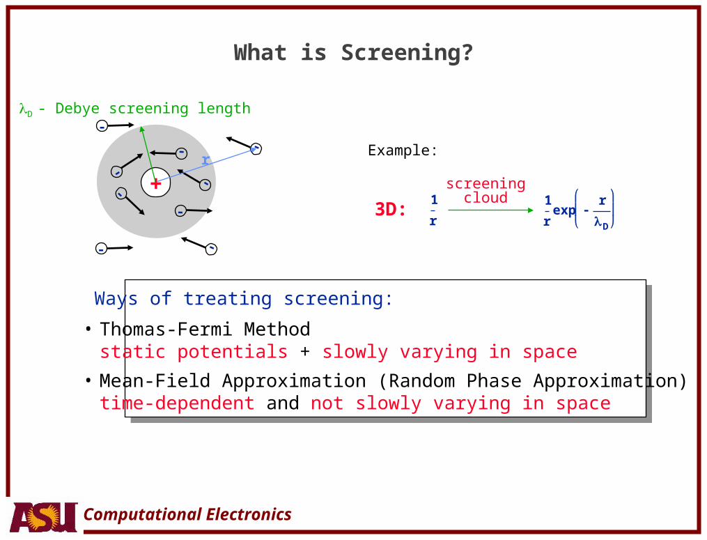
What is Screening?
+
-
--
-
-
-
-
-
-
D - Debye screening length
Ways of treating screening:
• Thomas-Fermi Methodstatic potentials + slowly varying in space
• Mean-Field Approximation (Random Phase Approximation)time-dependent and not slowly varying in space
r
3D: 1
r
1
rexp
r
D
screeningcloud
Example:
Computational Electronics
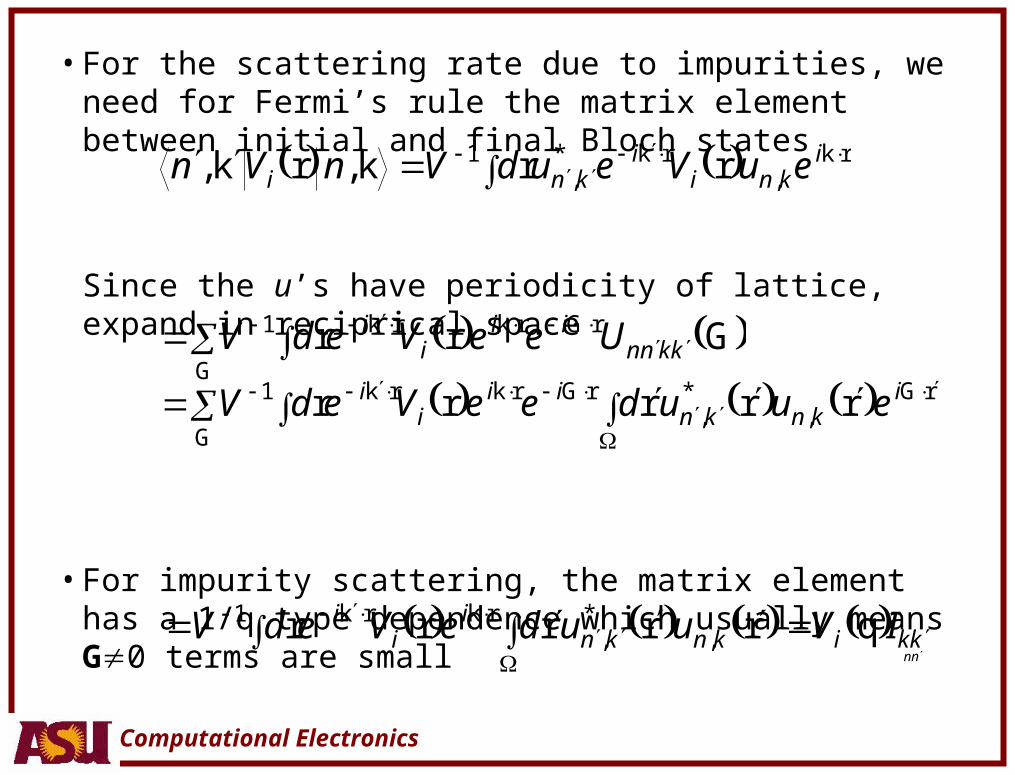
• For the scattering rate due to impurities, we need for Fermi’s rule the matrix element between initial and final Bloch states
Since the u’s have periodicity of lattice, expand in reciprical space
• For impurity scattering, the matrix element has a 1/q type dependence which usually means G0 terms are small
rkrk1 rrkrk
ikni
ikni euVeudVnVn ,
*,,,
Grr rG
G
rkrk1kknn
iii
i UeeVedV
rGrG
G
rkrk1 rrrrr iknkn
iii
i euudeeVedV ,*
,
nnkkiknkn
ii
i IVuudeVedV
qrrrrr rkrk1,
*,
Computational Electronics
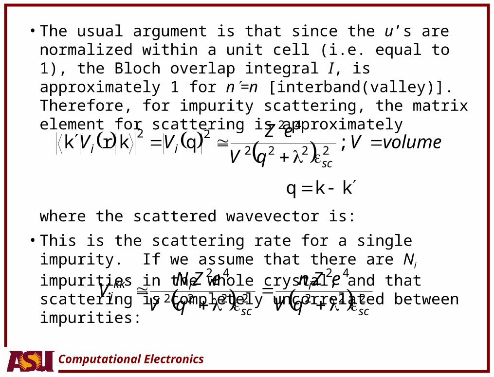
• The usual argument is that since the u’s are normalized within a unit cell (i.e. equal to 1), the Bloch overlap integral I, is approximately 1 for n=n [interband(valley)]. Therefore, for impurity scattering, the matrix element for scattering is approximately
where the scattered wavevector is:
• This is the scattering rate for a single impurity. If we assume that there are Ni impurities in the whole crystal, and that scattering is completely uncorrelated between impurities:
where ni is the impurity density (per unit volume).
kkq
volumeVqV
eZVV
scii
;2222
4222
qkrk
222
42
2222
42
sc
i
sc
ikki qV
eZn
qV
eZNV
Computational Electronics
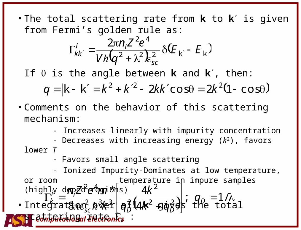
• The total scattering rate from k to k is given from Fermi’s golden rule as:
If is the angle between k and k, then:
• Comments on the behavior of this scattering mechanism:
- Increases linearly with impurity concentration- Decreases with increasing energy (k2), favors lower T- Favors small angle scattering
- Ionized Impurity-Dominates at low temperature, or room temperature in impure samples (highly doped regions)
• Integration over all k gives the total scattering rate k :
kk222
422EE
qV
eZn
sc
iikk
coscos 122kk 222 kkkkkq
/;*
14
4
8 222
2
332
42
DDDsc
iik q
qkq
k
k
meZn
Computational Electronics
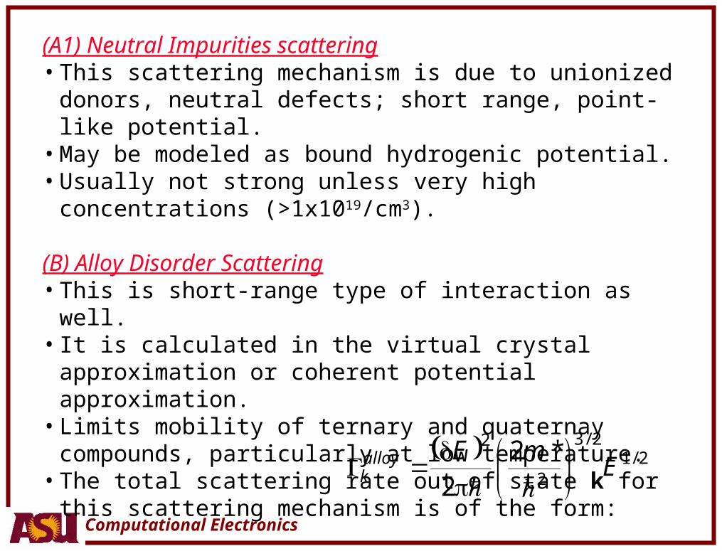
(A1) Neutral Impurities scattering• This scattering mechanism is due to unionized donors, neutral
defects; short range, point-like potential.• May be modeled as bound hydrogenic potential.• Usually not strong unless very high concentrations
(>1x10¹⁹/cm3).
(B) Alloy Disorder Scattering• This is short-range type of interaction as well.• It is calculated in the virtual crystal approximation or coherent
potential approximation.• Limits mobility of ternary and quaternay compounds,
particularly at low temperature.• The total scattering rate out of state k for this scattering
mechanism is of the form: 21
23
2
2 22
//*
EmEalloy
k
Computational Electronics
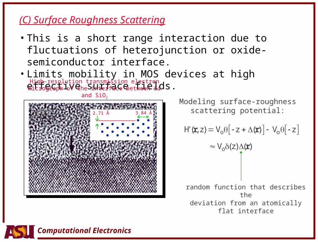
(C) Surface Roughness Scattering
• This is a short range interaction due to fluctuations of heterojunction or oxide-semiconductor interface.
• Limits mobility in MOS devices at high effective surface fields.
High-resolution transmission electron micrograph of the interface between Si and SiO2
(Goodnick et al., Phys. Rev. B 32, pp. 8171, 1985)
2.71 Å 3.84 Å
Modeling surface-roughnessscattering potential:
H'(r,z)Vo z (r) Vo z
Vo(z)(r)
random function that describes thedeviation from an atomically flat interface
Computational Electronics
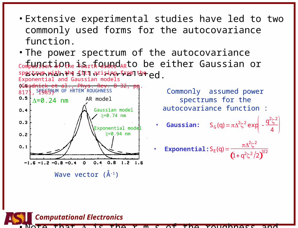
• Extensive experimental studies have led to two commonly used forms for the autocovariance function.
• The power spectrum of the autocovariance function is found to be either Gaussian or exponentially correlated.
• Note that is the r.m.s of the roughness and is the rough-ness correlation length.
Commonly assumed power spectrums for the autocovariance function :
• Gaussian: SG(q)22 exp q22
4
• Exponential: SE(q)22
1 q22 2 3 2
Wave vector (Å-1)
AR model
Gaussian model=0.74 nm
Exponential model=0.94 nm
=0.24 nm
SPECTRUM OF HRTEM ROUGHNESS
Comparison of the fourth-order AR spectrum with the fits arising from the Exponential and Gaussian models(Goodnick et al., Phys. Rev. B 32, pp. 8171, 1985)
Computational Electronics
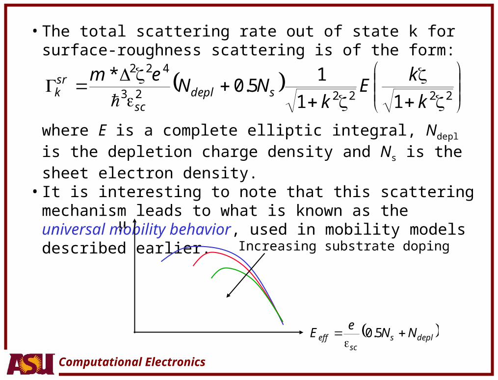
• The total scattering rate out of state k for surface-roughness scattering is of the form:
where E is a complete elliptic integral, Ndepl is the depletion charge density and Ns is the sheet electron density.
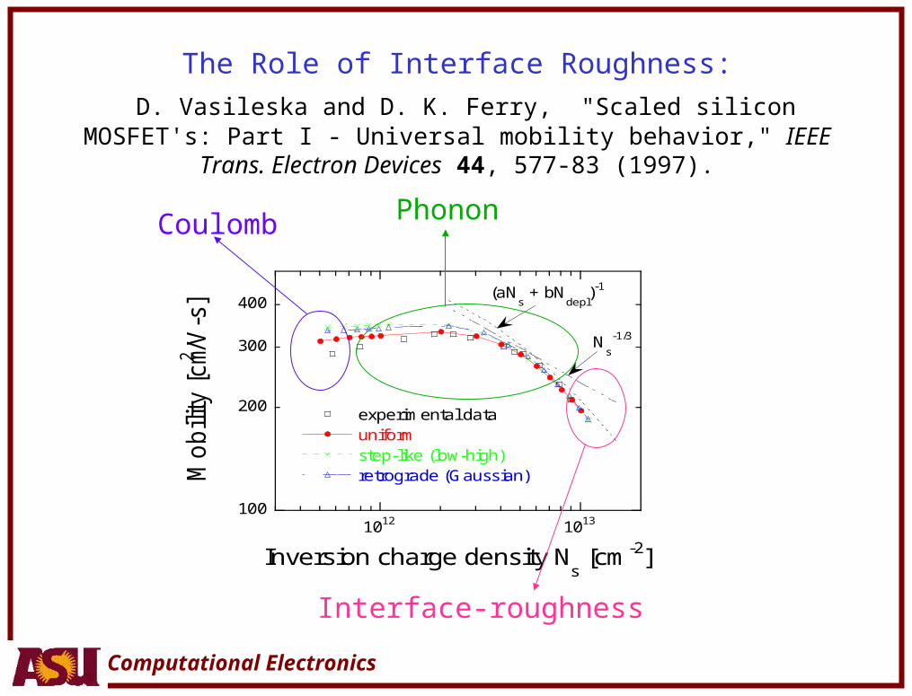
• It is interesting to note that this scattering mechanism leads to what is known as the universal mobility behavior, used in mobility models described earlier.
222223
422
11
150
k
kE
kNN
emsdepl
sc
srk .
*
deplssc
eff NNe
E
50.
Increasing substrate doping
Computational Electronics
100
200
300
400
1012 1013
experimental datauniformstep-like (low-high)retrograde (Gaussian)M
obili
ty [cm2 /V
-s]
Inversion charge density Ns [cm-2]
(aNs + bN
depl)-1
Ns
-1/3
PhononCoulomb
Interface-roughness
The Role of Interface Roughness:
D. Vasileska and D. K. Ferry, "Scaled silicon MOSFET's: Part I - Universal mobility behavior," IEEE Trans. Electron Devices 44, 577-83 (1997).
Computational Electronics
C.2 Inelastic Scattering MechanismsC.2 Inelastic Scattering Mechanisms
C.2.1 Some general considerations
• The Electron Lattice Hamiltonian is of the following form:
where Bloch states
• For the lattice Hamiltonian we have:
couplingPhononElectronH
nHamiltonialatticeHnHamiltoniaElectronH
HHHH
ep
le
eple
;
krk
kkkk ,,,,, ni
nnnne ueEH
21
q
3q2q1q
nE
nnnEH
l
lllll
,
...
Second quantized representation, where nq is the number of phonons with wave-vector q, mode .
Computational Electronics
• Phonons:
The Fourier expansion in reciprocal space of the coupled vibrational motion of the lattice decouples into normal modes which look like an independent set of Harmonic oscillators with frequency
q
labels the mode index, acoustic (longitudinal, 2 transverse modes) or optical (1 longitudinal, 2 transverse)
q labels the wavevector corresponding to traveling wave solutions for individual components,
• The velocity and the occupancy of a given mode are given by:
ondistributiEinsteinBosee
nlBTk
;
/ 1
1q
q
qv qq
Computational Electronics
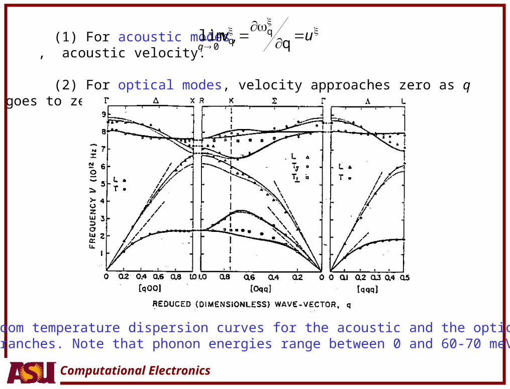
(1) For acoustic modes, , acoustic velocity.
(2) For optical modes, velocity approaches zero as q goes to zero.
u
q qv qq
0lim
Room temperature dispersion curves for the acoustic and the opticalbranches. Note that phonon energies range between 0 and 60-70 meV.
Computational Electronics
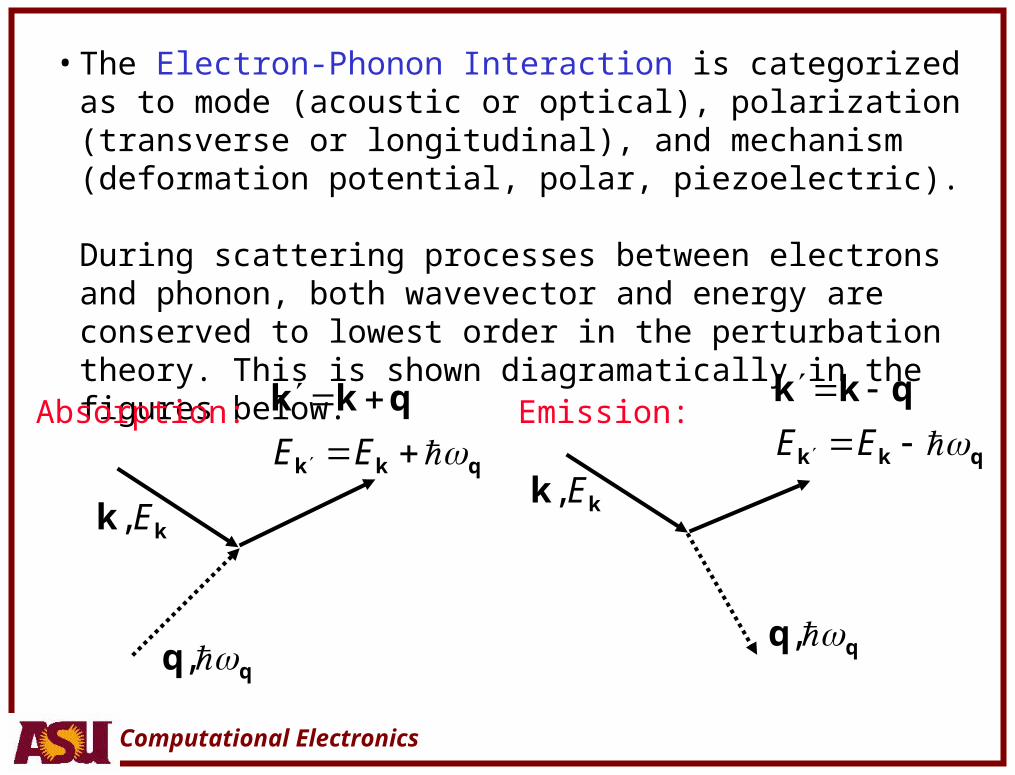
• The Electron-Phonon Interaction is categorized as to mode (acoustic or optical), polarization (transverse or longitudinal), and mechanism (deformation potential, polar, piezoelectric).
During scattering processes between electrons and phonon, both wavevector and energy are conserved to lowest order in the perturbation theory. This is shown diagramatically in the figures below.
Absorption: Emission:
kk E, kk E,qkk
qkk
EE
qq , qq ,
qkk
qkk
EE
Computational Electronics
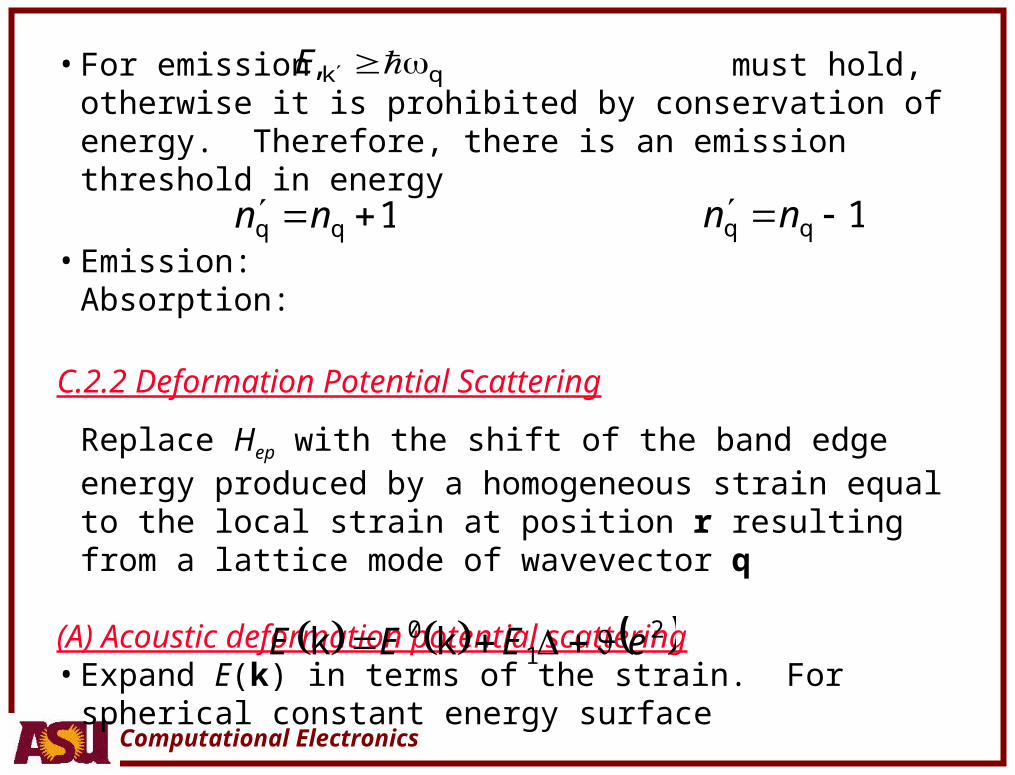
• For emission, must hold, otherwise it is prohibited by conservation of energy. Therefore, there is an emission threshold in energy
• Emission: Absorption:
C.2.2 Deformation Potential Scattering
Replace Hep with the shift of the band edge energy produced by a homogeneous strain equal to the local strain at position r resulting from a lattice mode of wavevector q
(A) Acoustic deformation potential scattering• Expand E(k) in terms of the strain. For spherical constant
energy surface
21
0 kk eEEE
qk E
1qq nn 1qq nn
Computational Electronics
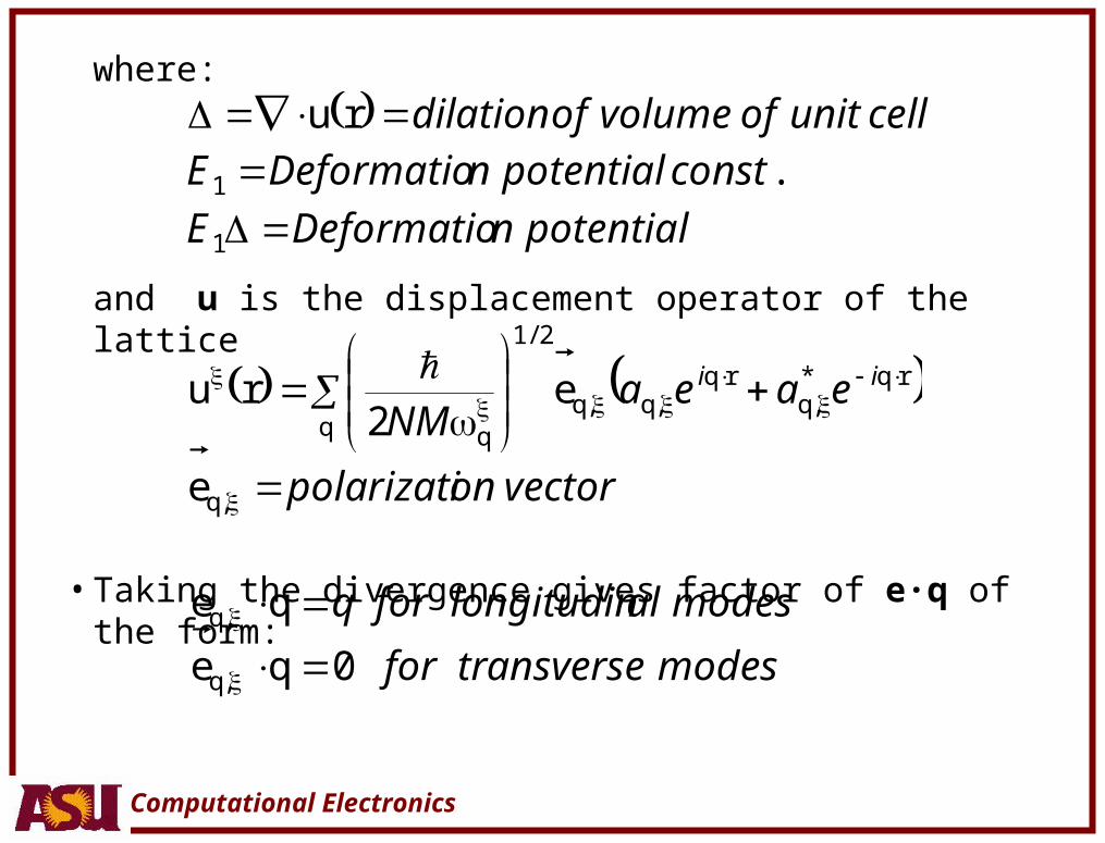
where:
and u is the displacement operator of the lattice
• Taking the divergence gives factor of e·q of the form:
Therefore, only longitudinal modes contribute.
vectoronpolarizati
eaeaNM
ii
,
*,,,
/
q
rqq
rqqq
21
q q
e
e2
ru
potentialnDeformatioE
constpotentialnDeformatioE
cellunitofvolumeofdilation
1
1
ru
.
modestransversefor
modesallongitudinforq
0qe
qe
q
q
,
,
Computational Electronics
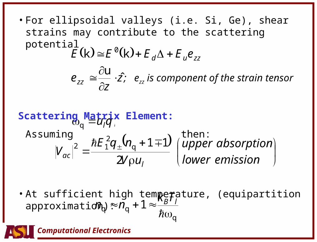
• For ellipsoidal valleys (i.e. Si, Ge), shear strains may contribute to the scattering potential
Scattering Matrix Element:
Assuming then:
• At sufficient high temperature, (equipartition approximation):
zz
e
eEEEE
zz
zzud
ˆ
u
kk 0
; ezz is component of the strain tensor
,qulq
emissionlower
absorptionupper
uV
nqEV
lac 2
11q212
qqq 1
lBTknn
Computational Electronics
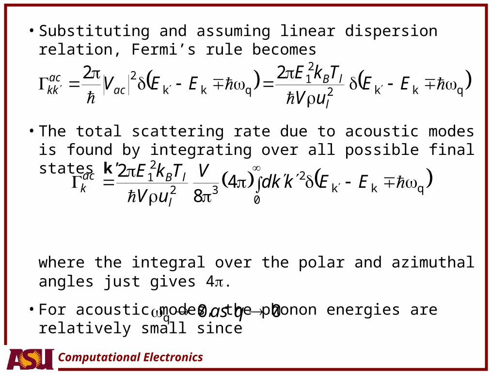
• Substituting and assuming linear dispersion relation, Fermi’s rule becomes
• The total scattering rate due to acoustic modes is found by integrating over all possible final states k’
where the integral over the polar and azimuthal angles just gives 4.
• For acoustic modes, the phonon energies are relatively small since
qkk2
21
qkk2 22
EEuV
TkEEEV
l
lBac
ackk
qkk0
232
21 4
8
2
EEkkd
V
uV
TkE
l
lBack
00q qas
Computational Electronics
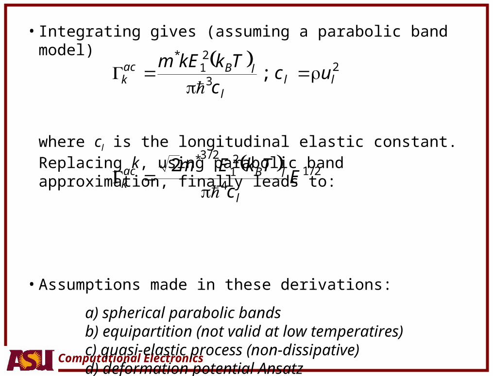
• Integrating gives (assuming a parabolic band model)
where cl is the longitudinal elastic constant. Replacing k, using parabolic band approximation, finally leads to:
• Assumptions made in these derivations:
a) spherical parabolic bands b) equipartition (not valid at low temperatires)c) quasi-elastic process (non-dissipative) d) deformation potential Ansatz
23
21
lll
lBack uc
c
TkkEm
;
*
214
21
232 /
/*
Ec
TkEm
l
lBack
Computational Electronics
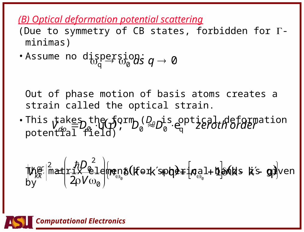
(B) Optical deformation potential scattering(Due to symmetry of CB states, forbidden for -minimas)• Assume no dispersion:
Out of phase motion of basis atoms creates a strain called the optical strain.
• This takes the form (D0 is optical deformation potential field)
The matrix element for spherical bands is given by
which is independent of q .
00q qas
orderzerothDDDVdo q000 eru ;
qkk1qkk2 00
0
20
2
nnVD
V ackk
Computational Electronics
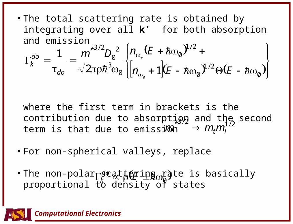
• The total scattering rate is obtained by integrating over all k’ for both absorption and emission
where the first term in brackets is the contribution due to absorption and the second term is that due to emission
• For non-spherical valleys, replace
• The non-polar scattering rate is basically proportional to density of states
021
0
210
03
20
23
12
1
0
0
EEn
EnDm
do
dok /
//*
2123 //*ltmmm
0 Edok
Computational Electronics
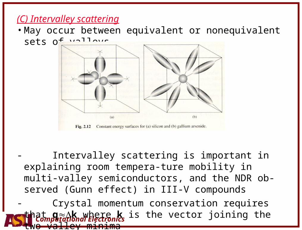
(C) Intervalley scattering• May occur between equivalent or nonequivalent sets of valleys
- Intervalley scattering is important in explaining room tempera-ture mobility in multi-valley semiconductors, and the NDR ob-served (Gunn effect) in III-V compounds
- Crystal momentum conservation requires that qk where k is the vector joining the two valley minima
Computational Electronics
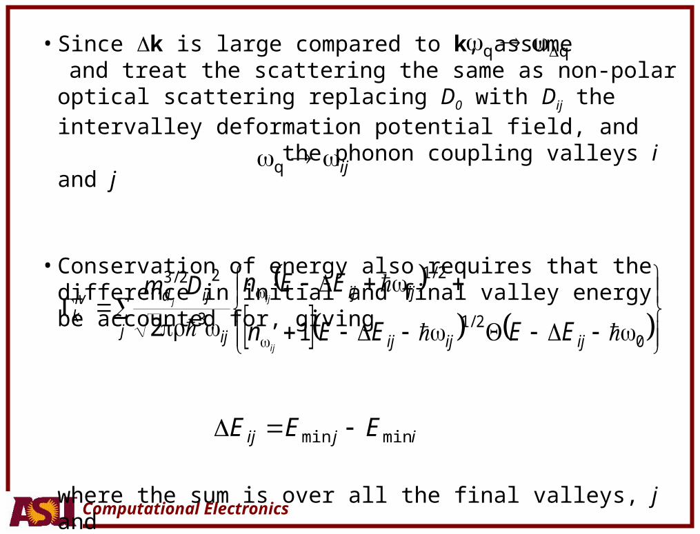
• Since k is large compared to k, assume and treat the scattering the same as non-polar optical scattering replacing D0 with Dij the intervalley deformation potential field, and the phonon coupling valleys i and j
• Conservation of energy also requires that the difference in initial and final valley energy be accounted for, giving
where the sum is over all the final valleys, j and
021
21
3
223
12
ijijij
ijij
j ij
ijdivk
EEEEn
EEnDm
ij
ijj
/
//
ijq
ijij EEE minmin
Computational Electronics
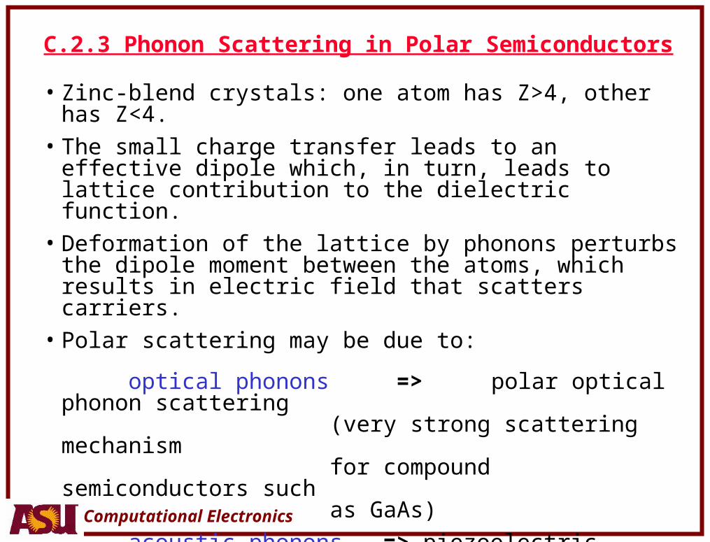
C.2.3 Phonon Scattering in Polar Semiconductors
• Zinc-blend crystals: one atom has Z>4, other has Z<4.
• The small charge transfer leads to an effective dipole which, in turn, leads to lattice contribution to the dielectric function.
• Deformation of the lattice by phonons perturbs the dipole moment between the atoms, which results in electric field that scatters carriers.
• Polar scattering may be due to:
optical phonons => polar optical phonon scattering(very strong scattering mechanismfor compound semiconductors
suchas GaAs)
acoustic phonons => piezoelectric scattering(important at low temperatures invery pure semiconductors)
Computational Electronics
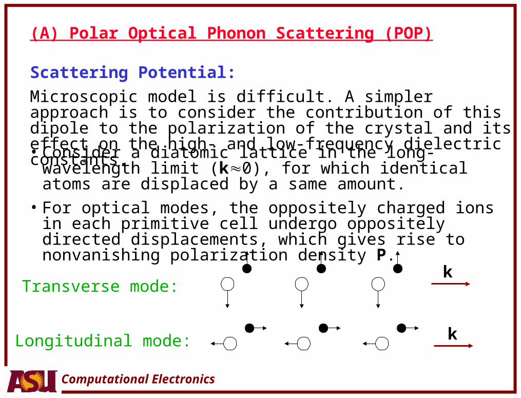
(A) Polar Optical Phonon Scattering (POP)
Scattering Potential:
Microscopic model is difficult. A simpler approach is to consider the contribution of this dipole to the polarization of the crystal and its effect on the high- and low-frequency dielectric constants.
• Consider a diatomic lattice in the long-wavelength limit (k0), for which identical atoms are displaced by a same amount.
• For optical modes, the oppositely charged ions in each primitive cell undergo oppositely directed displacements, which gives rise to nonvanishing polarization density P.
kTransverse mode:
kLongitudinal mode:
Computational Electronics
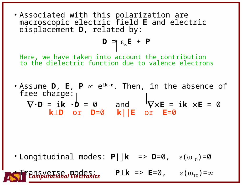
• Associated with this polarization are macroscopic electric field E and electric displacement D, related by:
D = E + P
• Assume D, E, P eik.r. Then, in the absence of free charge:
·D = ik ·D = 0 and E = ik E = 0
• Longitudinal modes: P||k => D=0, (LO)=0
• Transverse modes: Pk => E=0, (TO)=
Here, we have taken into account the contributionto the dielectric function due to valence electrons
kD or D=0 k||E or E=0
Computational Electronics
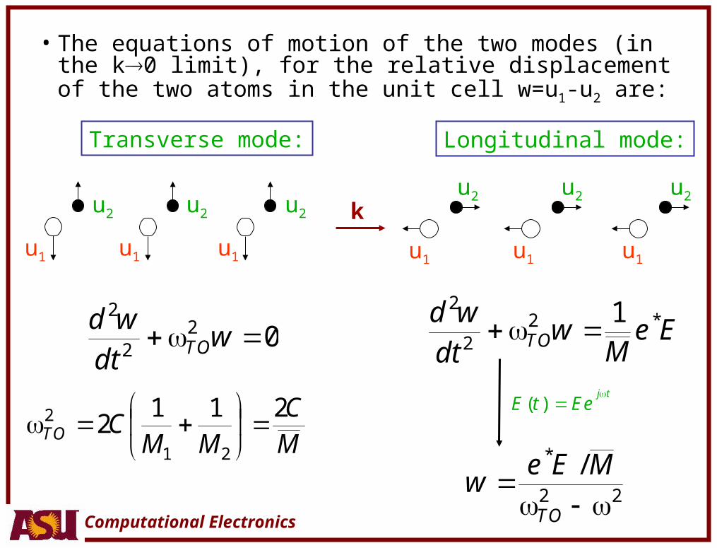
• The equations of motion of the two modes (in the k0 limit), for the relative displacement of the two atoms in the unit cell w=u1-u2 are:
Transverse mode: Longitudinal mode:
k
u1 u1 u1
u2 u2 u2
022
2
wdt
wdTO
MC
MMCTO
2112
21
2
u1 u1 u1
u2 u2 u2
EeM
wdt
wdTO
*122
2
22
TO
MEew
/*
tjEetE
)(
Computational Electronics
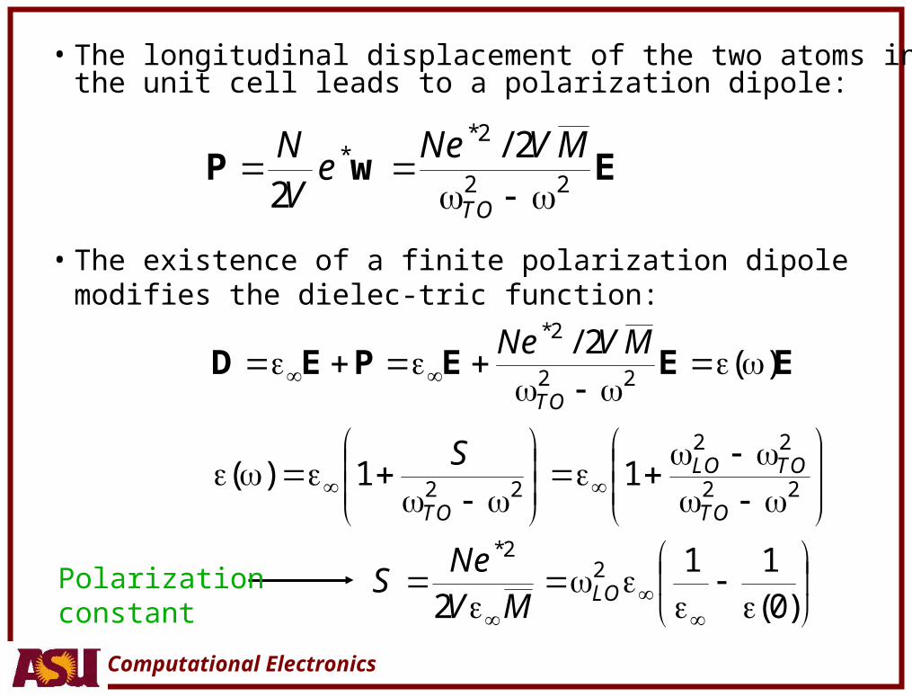
• The longitudinal displacement of the two atoms in the unit cell leads to a polarization dipole:
EwP 22
2 22
TO
MVNee
VN /*
*
• The existence of a finite polarization dipole modifies the dielec-tric function:
)(
)(
)(/
*
*
011
2
11
2
22
22
22
22
22
2
LO
TO
TOLO
TO
TO
MVNe
S
S
MVNe
EEEPED
Polarizationconstant
Computational Electronics
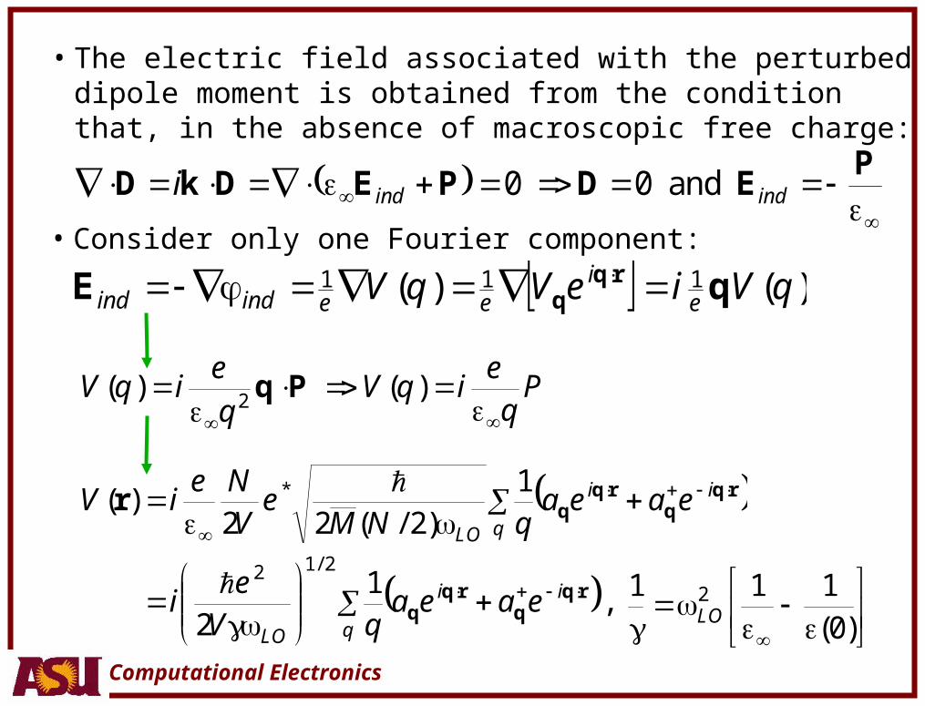
• The electric field associated with the perturbed dipole moment is obtained from the condition that, in the absence of macroscopic free charge:
P
ED PEDkD indindi and 00
• Consider only one Fourier component:
)()( qVieVqV ei
eeindind qE rqq
111
Pq Pq
eiqV
q
eiqV
)()( 2
,
)/()(
/
*
r
rqq
rqq
rqq
rqq
ii
qLO
ii
qLO
eaeaqV
ei
eaeaqNM
eVNe
iV
12
1222
212
)(0
111 2LO
Computational Electronics
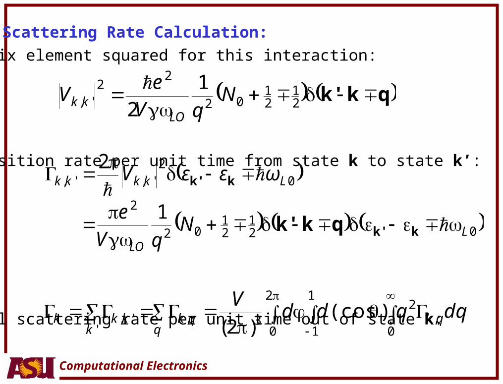
• Matrix element squared for this interaction:
• Transition rate per unit time from state k to state k’:
• Total scattering rate per unit time out of state k:
qkk'
21
21
02
22 1
2N
qVe
VLO
kk ',
Scattering Rate Calculation:
021
21
02
2
02
1
2
LLO
Lkkkk
NqV
e
ωεεV
kk'
kk'
qkk'
',',
dqqddV
qkq
qkk
kkk ,,'
', )(cos)(
2
0
1
1 0
232
Computational Electronics
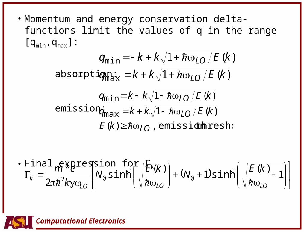
• Momentum and energy conservation delta-functions limit the values of q in the range [qmin,qmax]:
absorption:
emission:
• Final expression for k
)(1
)(1
max
min
kEkkq
kEkkq
LO
LO
thresholdemission,)(
)(1
)(1
max
min
LO
LO
LO
kE
kEkkq
kEkkq
112
10
102
2
LOLOLOk
kEN
kEN
k
em
)(sinh
)(sinh
*
Computational Electronics
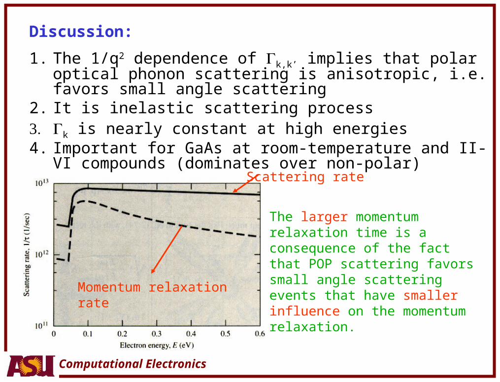
Discussion:
1. The 1/q2 dependence of k,k’ implies that polar optical phonon scattering is anisotropic, i.e. favors small angle scattering
2. It is inelastic scattering process3. k is nearly constant at high energies4. Important for GaAs at room-temperature and II-VI compounds
(dominates over non-polar)
Scattering rate
Momentum relaxationrate
The larger momentum relaxation time is a consequence of the fact that POP scattering favors small angle scattering events that have smaller influence on the momentum relaxation.
Computational Electronics
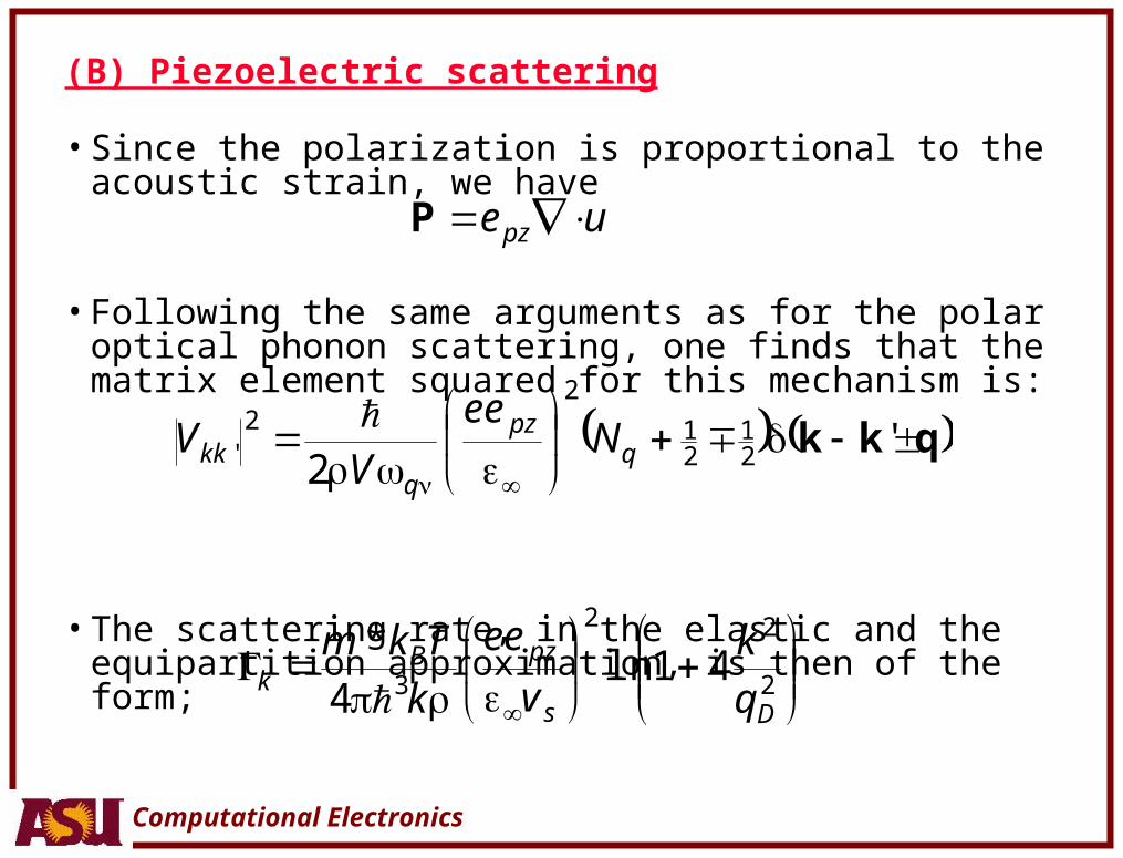
(B) Piezoelectric scattering
• Since the polarization is proportional to the acoustic strain, we have
• Following the same arguments as for the polar optical phonon scattering, one finds that the matrix element squared for this mechanism is:
• The scattering rate, in the elastic and the equipartition approximation, is then of the form;
where qD is the screening wavevector.
uepz P
qkk
'' 21
21
22
2
qpz
qkk N
ee
VV
2
22
3 414 Ds
pzBk q
kv
ee
k
Tkmln
*
Computational Electronics
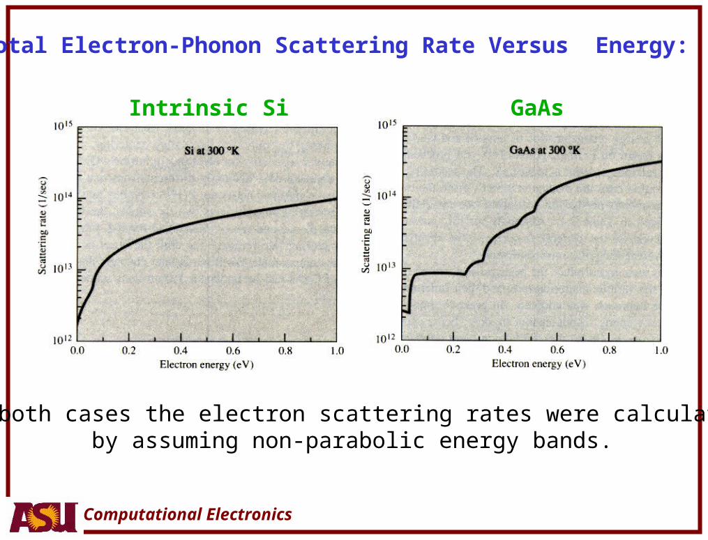
Total Electron-Phonon Scattering Rate Versus Energy:
Intrinsic Si GaAs
In both cases the electron scattering rates were calculatedby assuming non-parabolic energy bands.
Computational Electronics
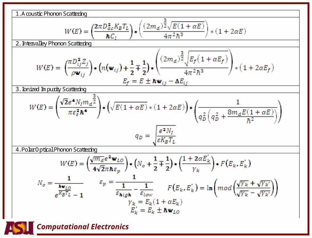
1. Acoustic Phonon Scattering
2. Intervalley Phonon Scattering
3. Ionized Impurity Scattering
4. Polar Optical Phonon Scattering
Computational Electronics
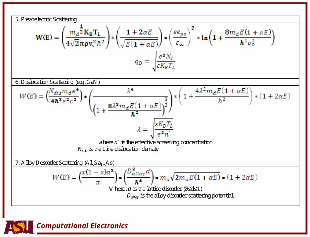
5. Piezoelectric Scattering
6. Dislocation Scattering (e.g. GaN)
where n’ is the effective screening concentration
Ndis is the Line dislocation density 7. Alloy Desorder Scattering (AlxGa1-xAs)
Where: d is the lattice disorder (0≤d≤1)
Dalloy is the alloy disorder scattering potential