comprehensive error analysis of ultra-wideband direct conversion receivers · 2007-06-19 ·...
TRANSCRIPT
Comprehensive error analysis of
ultra-wideband direct conversion receivers 1
Heiko Kopmann ∗, Heinz G. Gockler
Digital Signal Processing Group, Ruhr-Universitat Bochum,
Universitatsstr. 150, D-44780 Bochum, Germany
Dedicated to Professor H.W. Schußler on the occasion of his 75th birthday
Abstract
In this contribution, the direct conversion receiver (DCR) has been revisited and itsproperties have thoroughly been studied in detail. Contrary to common practice,our main interest is focused on the investigation of DCR performance degradation inconjunction with the processing of ultra-wideband FDM-signals. To this end, all po-tential DCR error sources have been identified and introduced into a comprehensiveerror model. This model encompasses delay, gain and phase errors, DC-offsets, bidi-rectional crosstalk between the input ports of the down-converters and, eventually,quantisation and clipping of the analogue-to-digital interface (ADI).
For all of these error sources an exact error analysis has been carried out and,in addition, compact and conveniently applicable formulae and design charts arepresented for the evaluation of the isolated impact of each of the various errorcontributions. Furthermore, a typical error scenario taken from an ultra-widebandapplication in satellite communications has been used to demonstrate the overallDCR performance degradation as a result of the combination of the most importanterror contributions. For this application, the major degradations are caused by delayerrors that are most pronounced in edge channels, DC-offsets that, however, heavilyimpair the channel centred about zero frequency only, and gain errors.
Key words: Direct conversion receiver (DCR), Analog-to-digital interface (ADI)
∗ Corresponding author. Tel.: +49-234-3227585; fax:+49-234-3214100.Email address: [email protected] (Heiko Kopmann).
1 This work has been supported by Tesat-Spacecom GmbH, Backnang, Germany.
1 Introduction
In communication systems that exchange information via band-pass channels,analogue subunits are more and more replaced with corresponding digitallyimplemented subsystems for long. This ongoing trend is due to the fact thatanalogue systems severely suffer from tolerance problems, temperature depen-dency, aging effects, etc. [21, 30]. In contrast, digital circuitry is exactly repro-ducible and, thus, completely free of all those deficiencies of analogue units.Moreover, digital circuits and systems can be highly integrated on small sizechips with low power consumption. Finally, since more and more information istransferred as digitised data (mobile phone, Internet, etc.), in communicationequipment an analogue-to-digital interface (ADI) is required anyhow.
As a consequence, in communication receivers of (modulated) band-pass sig-nals the interface between analogue and digital signal processing is shifted asclose as possible to the receiver’s front end (antenna, optical / electrical inter-face, etc.). In this context the following three receiver approaches are presentlydiscussed and investigated:
(1) In the Ideal Receiver [3, 20] the input band-pass signal is, after band lim-itation and amplification at its original allocation in the radio frequency(RF) band, directly (sub-) sampled, digitised and, thus, shifted to someintermediate frequency (IF) position in the digital domain [11, 20, 21, 30].Final down-conversion and channel selection is completely performed bydigital signal processing.
Depending on the highest frequency of the RF band-pass signal theallowable ADI-aperture jitter is that extremely small that this approachis not feasible up to now [28, 34, 35]. This seems to remain valid also forthe foreseeable future, even if time-interleaved ADIs [15, 16, 23] or/andsuitable error correction methods are applied [24].
(2) The Digital Receiver [20] is based on the superheterodyne principle. Byextensive analogue preprocessing, the RF band-pass input signal is fre-quency-shifted to some appropriately low IF position in one or even moreinterim steps of down-conversion. For the subsequent ADI and the digitalsignal processing the concept of the ideal receiver is applied.
This digital receiver approach is widely used in practical implemen-tations [11, 20]. The requirement on the ADI can be met by presenttechnology for signal bandwidths up to some tens of MHz, if the ana-logue IF is low enough. However, low IF generally requires at least twosuccessive steps of analogue down-conversion in conjunction with expen-sive band-pass filtering for good image suppression (narrow transitionregion). In general, these IF filters cannot be integrated on a chip. As aresult, volume and power consumption of analogue preprocessing is oftenprohibitive (e.g. for mobile phones and satellite communications). Con-
2
trary, by applying only one analogue down-conversion with higher IF, theADI problems tend to approach those of the ideal receiver.
(3) In the Direct Conversion Receiver (DCR) - also Homodyne and Zero-
IF Receiver - the incoming band-pass signal is immediately shifted tozero centre frequency [2, 20, 25, 26]. This approach applies two identicalmixers controlled by quadrature carriers with 900 phase offset in orderto extract the complex envelope [20, 21, 30] from the original band-passsignal. Analogue anti-aliasing filtering (to remove the mixer products atfrequencies above the local oscillator frequency) and digitising of the in-phase and quadrature components of the zero-IF signal is performed inparallel by a pair of identical low-pass filters cascaded with concurrentanalogue-to-digital converters (ADCs). Subsequent channel selection isachieved by digital base band processing.
With the DCR the amount of bulky and power consumptive multi-stageanalogue pre-processing units is reduced to a minimum. This is due to thefact that, contrary to the Digital Receiver, final channel selection filteringis mainly carried out in the digital domain. In addition, band limitationin front of the ADI requires less stringent low-pass rather than band-pass filtering. Finally, since digitisation of a complex envelope allows thelowest possible sampling rate [21], efficient oversampling techniques withpartly digital anti-aliasing filters [11, 31] can advantageously be appliedto a wide range of bandwidths.
Contrary to the merits quoted above, the DCR may suffer from severedistortions due to the fact that the transfer characteristics of the partlyanalogue in-phase and quadrature paths cannot be made identical. Fur-thermore, crosstalk between the various analogue branches of the double-output down-converter including the ADCs (signal paths and/or localoscillator and clock sources) introduces additional performance degra-dation (cf. e.g. [19a, 29]). All these deteriorations are getting still morepronounced with increasing signal bandwidth.
The above discussion reveals the DCR architecture as the most promisingcandidate for applications with stringent requirements on volume and powerconsumption. Hence, most recently, the DCR is increasingly considered asa baseline approach in GSM mobile phones as well as in more challengingsoftware radio applications including the UMTS standard with extended signalbandwidth [3, 20, 25, 26]. Presently, the experience with DCR gained so far andthe expected improvement of technology [34, 35] encourages the introductionof the DCR architecture, for instance, in satellite communications for on-boardprocessing of ultra-wideband FDM-signals. The envisaged overall bandwidthsrange from hundreds of MHz up to about 1GHz [8, 17].
The latter extremely challenging DCR application obviously calls for powerfulmeasures of error correction to meet the specified performance requirements(cf. e.g. [1, 4, 5, 7, 14, 16, 19b, 22, 23, 27, 32, 33]). In order to find robust meth-
3
ods of performance optimisation, at first, however, a thorough understandingof all relevant DCR error mechanisms is compulsory. Hence, in this first of sev-eral related publications, a comprehensive error analysis of the ultra-widebanddirect conversion receiver is developed. To this end, the ideal operation of aDCR is recalled in the following section. In the subsequent main section thevarious DCR error contributions are identified and introduced into a compre-hensive error model. Finally, this error model is applied to study the impactof parameter deviation on performance (signal to noise and distortion ratio)degradation.
2 The ideal direct conversion receiver
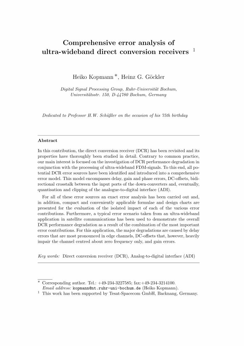
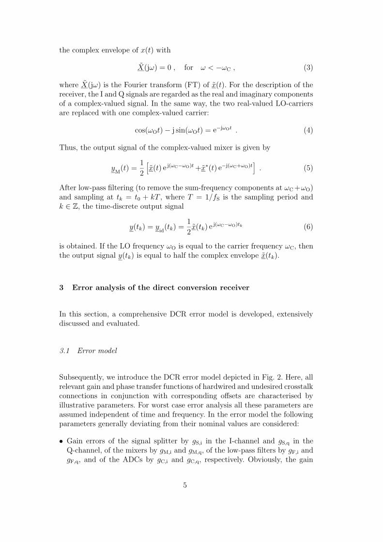
Fig. 1 shows the block diagram of the ideal DCR up to the ADI. The inputsignal x(t) is split into two channels. In one channel, the so-called in-phase orI-channel, the signal is mixed with a sinusoidal carrier derived from a localoscillator (LO) of frequency ωO. The signal in the so-called quadrature or Q-channel is mixed with the LO carrier of the same frequency but with 900 phaseoffset. The resulting channel signals are band-limited by an anti-aliasing filterand A-to-D converted for subsequent digital signal processing.
In the following analytical investigation of the functional principle an arbi-trarily modulated input signal
x(t) = Re
a(t) e j(ωCt+ϕ(t))
= Re
x(t) e jωCt
=1
2
[
x(t) ejωCt +x∗(t) e−jωCt]
(1)is assumed, where ωC represents the carrier frequency, x∗(t) the complex con-jugate of x(t), and
x(t) = a(t) e jϕ(t) , a(t) > 0 ∀t (2)
x t( )
~~~
90°
w0
AD
y ti( )k
~~ yq( )tk
~~
AD
Fig. 1. Ideal DCR including ADI
4
the complex envelope of x(t) with
X(jω) = 0 , for ω < −ωC , (3)
where X(jω) is the Fourier transform (FT) of x(t). For the description of thereceiver, the I and Q signals are regarded as the real and imaginary componentsof a complex-valued signal. In the same way, the two real-valued LO-carriersare replaced with one complex-valued carrier:
cos(ωOt) − j sin(ωOt) = e−jωOt . (4)
Thus, the output signal of the complex-valued mixer is given by
yM
(t) =1
2
[
x(t) e j(ωC−ωO)t +x∗(t) e−j(ωC+ωO)t]
. (5)
After low-pass filtering (to remove the sum-frequency components at ωC +ωO)and sampling at tk = t0 + kT , where T = 1/fS is the sampling period andk ∈ Z, the time-discrete output signal
y(tk) = yid(tk) =
1
2x(tk) e j(ωC−ωO)tk (6)
is obtained. If the LO frequency ωO is equal to the carrier frequency ωC, thenthe output signal y(tk) is equal to half the complex envelope x(tk).
3 Error analysis of the direct conversion receiver
In this section, a comprehensive DCR error model is developed, extensivelydiscussed and evaluated.
3.1 Error model
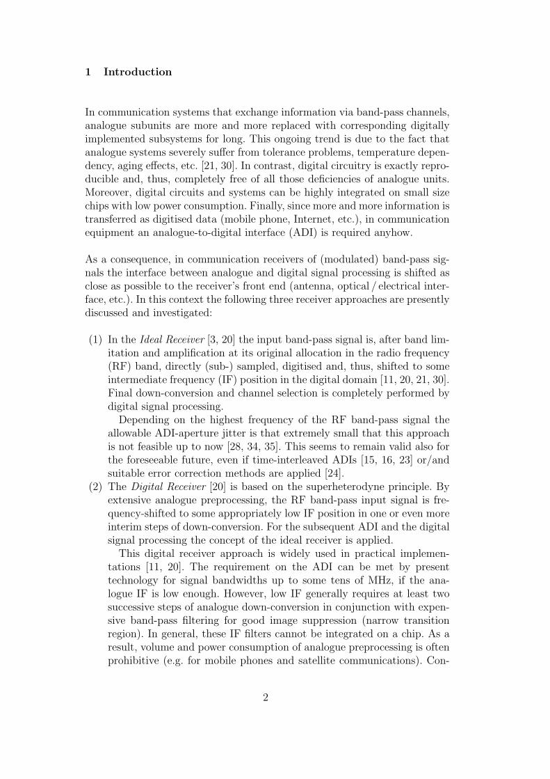
Subsequently, we introduce the DCR error model depicted in Fig. 2. Here, allrelevant gain and phase transfer functions of hardwired and undesired crosstalkconnections in conjunction with corresponding offsets are characterised byillustrative parameters. For worst case error analysis all these parameters areassumed independent of time and frequency. In the error model the followingparameters generally deviating from their nominal values are considered:
• Gain errors of the signal splitter by gS,i in the I-channel and gS,q in theQ-channel, of the mixers by gM,i and gM,q, of the low-pass filters by gF,i andgF,q, and of the ADCs by gC,i and gC,q, respectively. Obviously, the gain
5
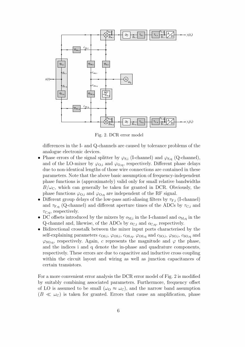
gM, q
oM, q
gF, i
x t( ) ~~~
90°
w0
AD
y ti( )k
~~ yq( )tk
+jO, q
jO, ijS, i
jS, q
gS, i
gS, qcOS, q
cOS, i
jOS, i
jOS, q
gM, i
gF, q
tF, i~~
tF, q
tC, igC, i
oC, i
AD
tC, qgC, q
oC, q
jSO, i
cSO, i
jSO, q
cSO, q
oM, i
Fig. 2. DCR error model
differences in the I- and Q-channels are caused by tolerance problems of theanalogue electronic devices.
• Phase errors of the signal splitter by ϕS,i (I-channel) and ϕS,q (Q-channel),and of the LO-mixer by ϕO,i and ϕO,q, respectively. Different phase delaysdue to non-identical lengths of those wire connections are contained in theseparameters. Note that the above basic assumption of frequency-independentphase functions is (approximately) valid only for small relative bandwidthsB/ωC, which can generally be taken for granted in DCR. Obviously, thephase functions ϕO,i and ϕO,q are independent of the RF signal.
• Different group delays of the low-pass anti-aliasing filters by τF,i (I-channel)and τF,q (Q-channel) and different aperture times of the ADCs by τC,i andτC,q, respectively.
• DC offsets introduced by the mixers by oM,i in the I-channel and oM,q in theQ-channel and, likewise, of the ADCs by oC,i and oC,q, respectively.
• Bidirectional crosstalk between the mixer input ports characterised by theself-explaining parameters cOS,i, ϕOS,i, cOS,q, ϕOS,q and cSO,i, ϕSO,i, cSO,q andϕSO,q, respectively. Again, c represents the magnitude and ϕ the phase,and the indices i and q denote the in-phase and quadrature components,respectively. These errors are due to capacitive and inductive cross couplingwithin the circuit layout and wiring as well as junction capacitances ofcertain transistors.
For a more convenient error analysis the DCR error model of Fig. 2 is modifiedby suitably combining associated parameters. Furthermore, frequency offsetof LO is assumed to be small (ωO ≈ ωC), and the narrow band assumption(B ωC) is taken for granted. Errors that cause an amplification, phase
6
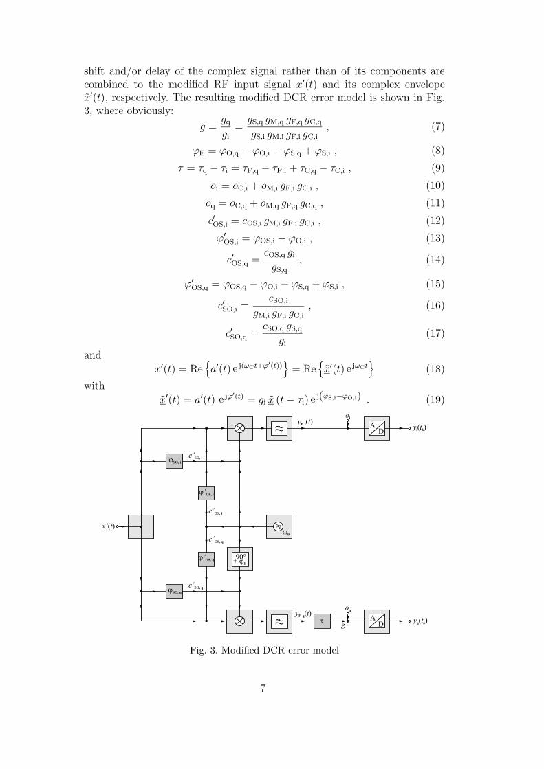
shift and/or delay of the complex signal rather than of its components arecombined to the modified RF input signal x′(t) and its complex envelopex′(t), respectively. The resulting modified DCR error model is shown in Fig.3, where obviously:
g =gq
gi
=gS,q gM,q gF,q gC,q
gS,i gM,i gF,i gC,i
, (7)
ϕE = ϕO,q − ϕO,i − ϕS,q + ϕS,i , (8)
τ = τq − τi = τF,q − τF,i + τC,q − τC,i , (9)
oi = oC,i + oM,i gF,i gC,i , (10)
oq = oC,q + oM,q gF,q gC,q , (11)
c′OS,i = cOS,i gM,i gF,i gC,i , (12)
ϕ′
OS,i = ϕOS,i − ϕO,i , (13)
c′OS,q =cOS,q gi
gS,q
, (14)
ϕ′
OS,q = ϕOS,q − ϕO,i − ϕS,q + ϕS,i , (15)
c′SO,i =cSO,i
gM,i gF,i gC,i
, (16)
c′SO,q =cSO,q gS,q
gi
(17)
and
x′(t) = Re
a′(t) e j(ωCt+ϕ′(t))
= Re
x′(t) e jωCt
(18)
with
x′(t) = a′(t) e jϕ′(t) = gi x (t − τi) e j(ϕS,i−ϕO,i) . (19)
x’ t( ) ~~~
90°
w0
AD
y ti( )k
~~ yq( )tk
+ jE
c’OS, q
c’OS, i
j OS, i’
j OS, q’
g
~~oi
AD
jSO, i
c’SO, i
jSO, q
c’SO, q
t
oq
y tF, q( )
y tF, i( )
Fig. 3. Modified DCR error model
7
3.2 Error analysis
In this section, the impact of the multitude of error sources on DCR perfor-mance is investigated by evaluating the modified DCR error model introducedabove. As a measure of performance the signal to noise and distortion ratio(SNDR) is adopted.
In order to determine the SNDR at the DCR (more precisely ADI) outputport, we start with calculating the DCR output signal. To this end, we firstintroduce the complex mixer output signal before anti-aliasing filtering by itsin-phase and quadrature components,
yM,i(t) =[
a′(t) cos (ωCt + ϕ′(t)) + c′OS,i cos(
ωOt + ϕ′
OS,i
)]
··[
cos (ωOt) + c′SO,i a′(t) cos (ωCt + ϕ′(t) + ϕSO,i)
]
(20)
and
yM,q(t) =[
a′(t) cos (ωCt + ϕ′(t)) + c′OS,q cos(
ωOt + ϕ′
OS,q
)]
··[
− sin (ωOt + ϕE) + c′SO,q a′(t) cos (ωCt + ϕ′(t) + ϕSO,q)]
, (21)
respectively. Using the trigonometrical identity
cos α cos β =1
2[cos(α − β) + cos(α + β)] , (22)
it follows after the subsequent ideal low-pass filtering:
yF,i(t) =1
2a′(t) cos (ωCt − ωOt + ϕ′(t)) +
+1
2c′OS,i cos
(
ϕ′
OS,i
)
+1
2c′SO,i [a′(t)]
2cos (ϕSO,i) +
+1
2c′OS,i c
′
SO,i a′(t) cos
(
ωCt − ωOt + ϕ′(t) + ϕSO,i − ϕ′
OS,i
)
(23)
and
yF,q(t) =1
2a′(t) sin (ωCt − ωOt + ϕ′(t) − ϕE) +
+1
2c′OS,q sin
(
ϕ′
OS,q − ϕE
)
+1
2c′SO,q [a′(t)]
2cos (ϕSO,q) +
+1
2c′OS,q c′SO,q a′(t) cos
(
ωCt − ωOt + ϕ′(t) + ϕSO,q − ϕ′
OS,q
)
. (24)
8
Finally, by using (19), we obtain at the DCR-ADI output ports the in-phasecomponent
yi(tk) = Re
y′
id(tk)
+1
2c′OS,i cos
(
ϕ′
OS,i
)
+ 2 c′SO,i cos (ϕSO,i)∣
∣
∣y′
id(tk)
∣
∣
∣
2+
+ c′OS,i c′
SO,iRe
y′
id(tk) e j(ϕSO,i−ϕ′
OS,i)
+ oi + ei(tk) (25)
and the quadrature component
yq(tk) = gIm
y′
id(tk − τ) e−jϕE
+
+g
2c′OS,q sin
(
ϕ′
OS,q − ϕE
)
+ 2 g c′SO,q cos (ϕSO,q)∣
∣
∣y′
id(tk − τ)
∣
∣
∣
2+
+ g c′OS,q c′SO,qRe
y′
id(tk − τ) e j(ϕSO,q−ϕ′
OS,q)
+ oq + eq(tk) , (26)
where similarly to (6)
y′
id(tk) =
1
2x′(tk) e j(ωC−ωO)tk . (27)
The error sequences ei(tk) and eq(tk) are due to the non-linear quantisationand overflow saturation errors of the ADCs in the I- and Q-channels, respec-tively. For convenience, these two baseband components are combined to thecomplex-valued signal y(tk) = yi(tk) + jyq(tk):
y(tk) = y′
id(tk) + j Im
g y′
id(tk − τ) e−jϕE −y′
id(tk)
+
+ 2 c′SO,i cos (ϕSO,i)∣
∣
∣y′
id(tk)
∣
∣
∣
2+ j 2 g c′SO,q cos (ϕSO,q)
∣
∣
∣y′
id(tk − τ)
∣
∣
∣
2+
+1
2c′OS,i c
′
SO,i y′
id(tk) e j(ϕSO,i−ϕ′
OS,i) +
+1
2c′OS,i c
′
SO,i
[
y′
id(tk)
]
∗
e−j(ϕSO,i−ϕ′OS,i) +
+ jg
2c′OS,q c′SO,q y′
id(tk − τ) e j(ϕSO,q−ϕ′
OS,q) +
+ jg
2c′OS,q c′SO,q
[
y′
id(tk − τ)
]
∗
e−j(ϕSO,q−ϕ′OS,q) +
+1
2c′OS,i cos
(
ϕ′
OS,i
)
+ jg
2c′OS,q sin
(
ϕ′
OS,q − ϕE
)
+ o + e(tk) , (28)
where
o = oi + j oq (29)
and
e(tk) = ei(tk) + j eq(tk) . (30)
9
In the common case of a noisy DCR input signal y′
id(tk) consists of a signal
component y′
id,S(tk) and a noise contribution y′
id,N(tk):
y′
id(tk) = y′
id,S(tk) + y′
id,N(tk) . (31)
Hence, by introducing (31) into (28), the ADI output signal becomes
y(tk) = yS(tk) + y
N(tk) (32)
consisting of the distorted (usable) signal:
yS(tk) =
1
2
[
1 + c′OS,ic′
SO,i ej(ϕSO,i−ϕ′
OS,i)]
y′
id,S(tk) +
+g
2
[
e−jϕE +j c′OS,qc′
SO,q e j(ϕSO,q−ϕ′OS,q)
]
y′
id,S(tk − τ) (33)
and the noise and distortion contribution:
yN(tk) = y
X(tk) + y
I(tk) + y
C(tk) + y
O(tk) + e(tk) , (34)
where
yX(tk) =
1
2
[
1 + c′OS,ic′
SO,i ej(ϕSO,i−ϕ′
OS,i)]
y′
id,N(tk) +
+g
2
[
e−jϕE +j c′OS,qc′
SO,q e j(ϕSO,q−ϕ′OS,q)
]
y′
id,N(tk − τ) (35)
represents the noise load of the DCR input signal transferred to the ADIoutput port,
yI(tk) =
1
2
[
1 + c′OS,ic′
SO,i e−j(ϕSO,i−ϕ′
OS,i)]
[
y′
id(tk)
]
∗
+
− g
2
[
e jϕE −j c′OS,qc′
SO,q e−j(ϕSO,q−ϕ′OS,q)
]
[
y′
id(tk − τ)
]
∗
(36)
the image component (i.e. crosstalk between the in-phase and quadrature com-ponents),
yC(tk) = 2 c′SO,i cos (ϕSO,i)
∣
∣
∣y′
id(tk)
∣
∣
∣
2+
+ j 2 g c′SO,q cos (ϕSO,q)∣
∣
∣y′
id(tk − τ)
∣
∣
∣
2(37)
the noise and distortion contributions due to crosstalk from the RF mixerinput ports to the LO inputs of the mixers and, finally,
yO(tk) =
1
2c′OS,i cos
(
ϕ′
OS,i
)
+ jg
2c′OS,q sin
(
ϕ′
OS,q − ϕE
)
+ o (38)
10
the DC component originating from crosstalk of the LO carriers to the RFinput ports of the mixers, and from the DC offsets of the ADCs and the mixers,respectively.
The SNDR is more easily determined in the frequency domain by using Par-seval’s relation [21, 30]. To this end, the time-domain signals derived aboveare subjected to the Fourier transform, where spectral representations are de-noted by capital letters. Introducing the combination of some errors accordingto the definitions
c′S(ω) = c′OS,ic′
SO,i ej(ϕSO,i−ϕ′
OS,i) +j g c′OS,qc′
SO,q e−j(ωτ−ϕSO,q+ϕ′OS,q) (39)
and
c′I(ω) = c′OS,ic′
SO,i e−j(ϕSO,i−ϕ′
OS,i) +j g c′OS,qc′
SO,q e−j(ωτ+ϕSO,q−ϕ′OS,q) , (40)
the resulting spectrum of the contaminated complex-valued DCR output sig-nal before sampling and quantisation is obtained:
Y (jω) = Y S(jω) + Y N(jω) , (41)
where
Y S(jω) =1
2
[
1 + g e−j(ωτ+ϕE) +c′S(ω)]
Y′
id,S(jω) (42)
represents the spectrum of the distorted (usable) signal and
Y N(jω) = Y X(jω) + Y I(jω) + Y C(jω) + Y O(jω) (43)
the spectrum of the noise and distortion contribution. Note that the spectralcontributions of (43) according to
Y X(jω) =1
2
[
1 + g e−j(ωτ+ϕE) +c′S(ω)]
Y′
id,N(jω) , (44)
Y I(jω) =1
2
[
1 − g e−j(ωτ−ϕE) +c′I(ω)] [
Y′
id(−jω)]∗
, (45)
Y C(jω) =1
π
[
c′SO,i cos (ϕSO,i) + j g c′SO,q cos (ϕSO,q) e−jωτ]
·
· Y′
id(jω) ∗[
Y′
id(−jω)]∗
(46)
and
Y O(jω) = π[
c′OS,i cos(
ϕ′
OS,i
)
+ j g c′OS,q sin(
ϕ′
OS,q − ϕE
)
+ 2 o]
δ(ω) (47)
represent the Fourier transforms of the signals (35)-(38).
11
Subsequently, we subject the time-discrete and quantised DCR-ADI outputsignal (32) in conjunction with (33)-(38) similarly to the discrete-time Fouriertransform (DTFT), equidistant sampling at
tk = t0 + kT with t0 = 0 (48)
and sufficient band-limitation in compliance with the sampling theorem pro-vided [21, 30]. Hence, the spectrum of the contaminated and distorted digitalDCR-ADI output signal y(tk) results in:
Y (ejΩ) = Y S(ejΩ) + Y N(ejΩ) (49)
with
Y S(ejΩ) =
1
T
∞∑
λ=−∞
Y S (jω − jλωS) (50)
and
Y N(ejΩ) =1
T
∞∑
λ=−∞
Y N (jω − jλωS) + E(ejΩ) , (51)
where Ω = ωT is the normalised frequency, ωS = 2π/T , and E(ejΩ) the spec-trum of e(tk).
Finally, for any channel denoted by c, the ADI output SNDR of the imperfectDCR is determined in the frequency domain by using Parseval’s relation:
SNDRY,c = 10 log10
PS,c
PN,c
= 10 log10
∫ Ωu,c
Ωl,c
∣
∣
∣Y S
(
ejΩ)∣
∣
∣
2dΩ
∫ Ωu,c
Ωl,c
∣
∣
∣Y N
(
ejΩ)∣
∣
∣
2dΩ
, (52)
where Ωl,c and Ωu,c represent the lower and upper cut-off frequencies of channelc, respectively.
3.3 Evaluation
In this section, the signal to noise and distortion ratio (52) is evaluated inconjunction with (39)-(51) using typical assumptions and parameters takenfrom an application in wideband satellite communications [17]:
• Crosstalk from the RF mixer input ports to the LO inputs of the mixerscan be neglected: c′SO,i = c′SO,q = 0.
• y′
id,S(tk) and y′
id,N(tk) as well as y
X(tk), y
I(tk), y
O(tk), eQ(tk) and eC(tk) are
uncorrelated, where eQ(tk) represents the quantisation error sequence andeC(tk) the error sequence due to clipping by overflow saturation (e(tk) =eQ(tk) + eC(tk)).
12
• Constant power spectral density of the following signals:· Power P ′
id,S,c of the usable signal in channel c of bandwidths Bc = fu,c−fl,c
and baseband centre frequency fC,c = (fu,c + fl,c)/2.· All inherent noise contributions due to quantisation and clipping including
the noise load of the DCR input signal.
Using these assumptions, the SNDR at the output of the DCR-ADI results in:
SNDRY,c = 10 log10
G2(pf)PS,c
G2(pf) [PX,c + PI,N,c + PI,S,c + PO,c] + PQ,c + PC,c
, (53)
where the contributions according to
PS,c =1
8πBc
P ′
id,S,c
∫ ωu,c
ωl,c
1 + g2 + 2g cos (ωτ + ϕE) dω
=1
4P ′
id,S,c
[
1 + g2 +g
πBcτ[sin (ωu,cτ + ϕE) − sin (ωl,cτ + ϕE)]
]
=1
4P ′
id,S,c
[
1 + g2 + 2g cos (ωC,cτ + ϕE) sinc (πBcτ)]
(54)
with sinc(x) = sin(x)/x,
PX,c =1
4P ′
id,N,c
[
1 + g2 + 2g cos (ωC,cτ + ϕE) sinc (πBcτ)]
, (55)
PI,S,c =1
4P ′
id,S,c∗
[
1 + g2 − 2g cos (ωC,c∗τ + ϕE) sinc (πBc∗τ)]
, (56)
PI,N,c =1
4P ′
id,N,c
[
1 + g2 − 2g cos (ωC,cτ − ϕE) sinc (πBcτ)]
(57)
and
PO,c =
PO if ωl,c ≤ 0 ≤ ωu,c ,
0 else(58)
with
PO =[
oi +1
2c′OS,i cos
(
ϕ′
OS,i
)
]2
+[
oq +g
2c′OS,q sin
(
ϕ′
OS,q − ϕE
)
]2
(59)
represent the various power spectra (42), (44), (45) and (47) in channel c,where the image component is split into a signal (56) and noise (57) part. In(56) it is, for simplicity, assumed that the signal of channel c is completelycontaminated by only that of the mirror channel c∗, where ωC,c∗ = −ωC,c
and Bc∗ = Bc. Note that this case is considered as the standard assumptionthroughout the remainder of this paper. By choosing ωC,c∗ 6= −ωC,c and / orBc∗ 6= Bc the above relations can be adapted to a more general scenario.
Next, we investigate the noise contributions to (53) due to the non-linear op-erations of clipping (PC,c) and quantisation (PQ,c). To this end, at the ADI
13
output ports overflow saturation by ±1 (C) is anticipated. Introducing iden-tical parametric peak factors pf [9, 10, 12, 13] for the in-phase (real) andquadrature (imaginary) components of the complex ADI input signal, we re-quire:
pf
√
Pid
2= C = 1 . (60)
The clipper output signal is decomposed into a linear part being correlatedwith the clipper input signal, and the non-linear portion that is uncorrelatedwith the input signal. For the linear part, we introduce the equivalent gain [6]
G(pf) = erf
(
pf√2
)
=2√π
∫
pf√2
0e−ξ2
dξ ≤ 1 . (61)
The clipper output power of the linear part is equal to the clipper input powermultiplied by G2(pf) (see Eq. (53)) and the non-linear part (clipping noise) [6]is characterised by
PC,c =2Bc
fS
1 −√
2
π
1
pf
e−p2f2 −
(
1 − 1
p2f
)
G (pf) −1
p2f
G2 (pf)
. (62)
Finally, the power of the quantisation noise is given by
PQ,c =Bc
12fS
[
q2i + q2
q
]
=Bc
3fS
[
2−2 wi + 2−2 wq
]
, (63)
where qi and qq represent the quantisation step sizes, and wi and wq thecorresponding word lengths of the ADCs in the I- and Q-channel, respectively.
For convenience, (53) is eventually rearranged. To this end, first (55) and (57)are combined:
PX,c + PI,N,c =1
2P ′
id,N,c
[
1 + g2 − 2g sin (ϕE) sin (ωC,cτ) sinc (πBcτ)]
. (64)
By inserting (54), (56) and (64) into (53) it follows
SNDRY,c = 10 log10
1 + g2 + 2g cos (ωC,cτ + ϕE) sinc (πBcτ)
d(65)
where
d =P ′
id,S,c∗
P ′
id,S,c
[
1 + g2 − 2g cos (ωC,c∗τ + ϕE) sinc (πBc∗τ)]
+4PO,c
P ′
id,S,c
+
+2 [1 + g2 − 2g sin (ϕE) sin (ωC,cτ) sinc (πBcτ)]
SNDR′
X,c
+4(
PQ,c + PC,c
)
G2(pf)P ′
id,S,c
(66)
14
is used for abbreviation and
SNDRX,c = 10 log10 SNDR′
X,c = 10 log10
Pid,S,c
Pid,N,c
= 10 log10
P ′
id,S,c
P ′
id,N,c
(67)
is the signal to noise and distortion ratio of channel c at the DCR input.
In the following subsections the impact of the different error sources on theSNDR are investigated separately.
3.3.1 Gain, phase and delay errors
For the investigation of this section, a channel c with carrier frequency fC,c
related to its baseband representation, the bandwidth Bc and the power P ′
id,S,c
is considered, which is contaminated by the image spectrum of the mirrorchannel c∗ with the same power P ′
id,S,c∗ = P ′
id,S,c, which is allocated at fC,c∗ =−fC,c and is of the same bandwidth Bc∗ = Bc.
Taking only into account the gain, phase and delay errors, respectively, gen-erating mere imaging errors, (65) is simplified in conjunction with (66) to
SNDRY,c(g, ϕE, τ) = 10 log10
1 + g2 + 2g cos (ωC,cτ + ϕE) sinc (πBcτ)
1 + g2 − 2g cos (ωC,cτ − ϕE) sinc (πBcτ).
(68)With the definition g = 1 + ∆g, the approximations cos x ≈ 1 − x2/2 andsinc x ≈ 1 − x2/6 together with the assumption that the errors are small, weobtain the approximation
SNDRY,c(g, ϕE, τ) ≈ 10 log10
4 (1 + ∆g)
∆g2 + (ωC,cτ − ϕE)2 + 13(πBcτ)2 . (69)
Furthermore, with 1 + ∆g ≈ e∆g a more convenient representation of (69)readily follows:
SNDRY,c(g, ϕE, τ) ≈− 10 log10
[
∆g2 + (ωC,cτ − ϕE)2 +1
3(πBcτ)2
]
+
+ 4.3∆g + 6.0 . (70)
Considering only the gain error, (68) reduces to
SNDRY,c(g) = 20 log10
∣
∣
∣
∣
∣
1 + g
1 − g
∣
∣
∣
∣
∣
(71)
and its approximation (70) to
SNDRY,c(g) ≈ −20 log10 |∆g| + 4.3∆g + 6.0 , (72)
15
10−3 10−2 10−1 100 1010
10
20
30
40
50
60
70
80
90
|g| / dB
SND
R /
dB
Fig. 4. SNDRY,c as a function of |g|;exact solution: solid, approximated so-lution: dotted
10−3 10−2 10−1 100 10120
30
40
50
60
70
80
90
100
110
|phase error| / °
SND
R /
dB
Fig. 5. SNDRY,c as a function of |ϕE|;exact solution: solid, approximated so-lution: dotted
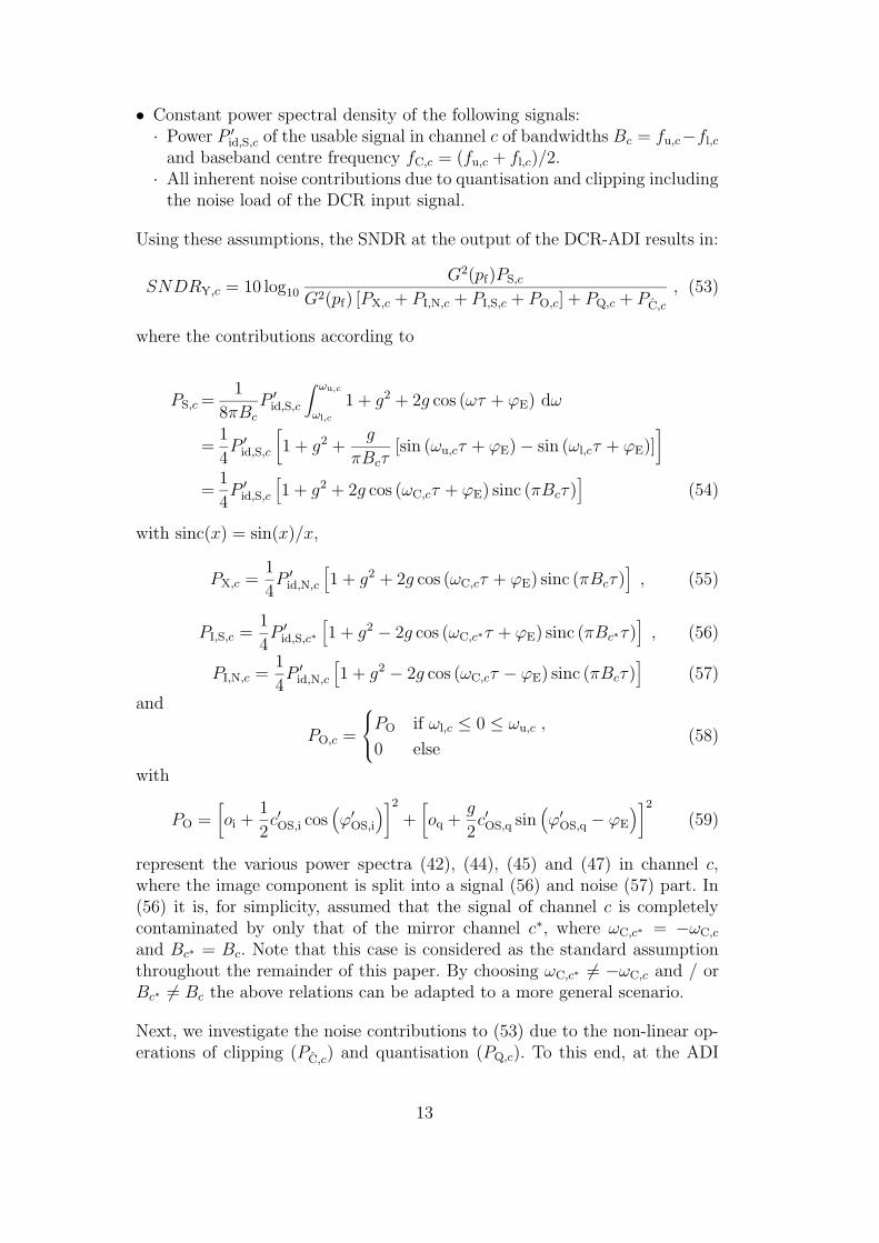
respectively. The exact and approximated SNDR according to (71) and (72)are shown in Fig. 4 as a function of |g|. The approximation (72) complies wellwith (71) for |g| < 3dB. By a (worst case) gain error |g| of 2.2dB [17] theSNDR attains 18.0dB.
Considering only the phase error, (68) is simplified to
SNDRY,c(ϕE) = 10 log10
1 + cos (ϕE)
1 − cos (ϕE)(73)
and (70) to
SNDRY,c(ϕE) ≈ −20 log10 |ϕE| + 6.0 , (74)
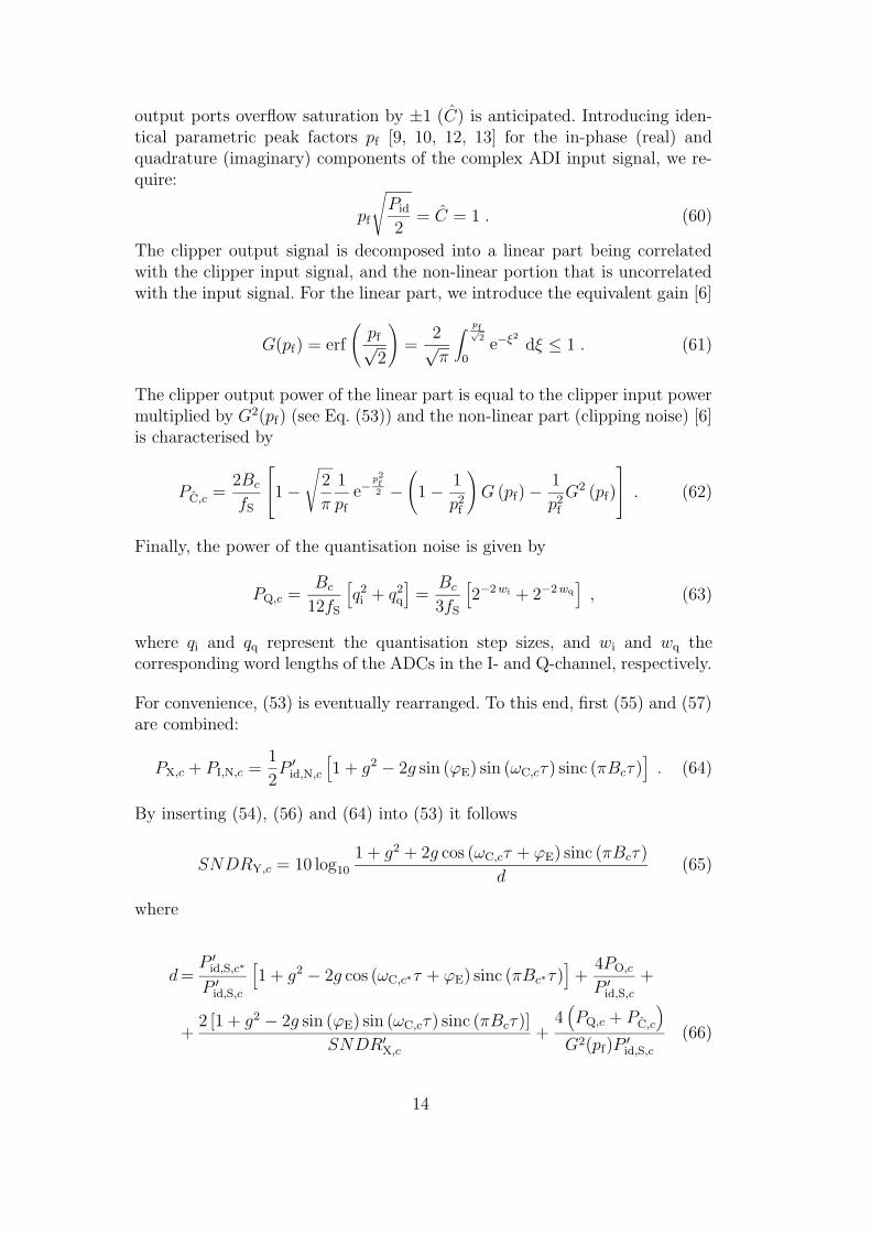
respectively. The SNDRs of (73) and (74) are depicted in Fig. 5. The approxi-mation (74) coincides very well with (73) in the displayed range. A phase error|ϕE| of 30 (worst case [17]) leads to an SNDR of 31.6dB.
Finally, if only the delay error is considered, (68) is reduced to
SNDRY,c(τ) = 10 log10
1 + cos (ωC,cτ) sinc (πBcτ)
1 − cos (ωC,cτ) sinc (πBcτ)(75)
and (70) to
SNDRY,c(τ) ≈ −20 log10 |τ | − 10 log10
(
f 2C,c +
1
12B2
c
)
− 9.9 (76)
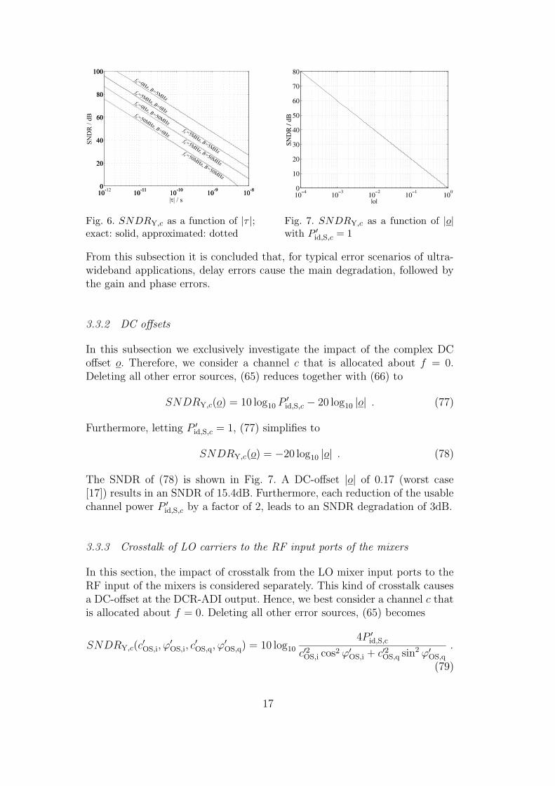
where τ is related to 1s and fC,c and Bc to 1Hz. The SNDRs of (75) and (76)are depicted in Fig. 6 as a function of |τ | for some pairs of carrier frequenciesfC,c and bandwidths Bc. The approximation (76) is consistent with (75) for lowfrequencies and small delay errors. Due to a delay error |τ | of 1.3ns (worst case[17]) in conjunction with carrier frequency fC,c and bandwidth Bc of 50MHzeach, the SNDR decreases to 13.3dB.
16
10-11
10-10
10-9
10-8
0
20
40
60
80
100
10-11
10-10
10-9
10-8
0
20
40
60
80
100
|t| / s
SN
DR
/d
B
10-
10-12
f
B
=0Hz,=5M
Hz
C
f
B
=5MHz,
=0Hz
C
f
B
=0Hz,=50M
Hz
C
f
B
=50MHz,
=0Hz
C
f
B
=50MHz,
=50MHz
C
f
B
=5MHz,
=50MHz
C
f
B
=5MHz,
=5MHz
C
Fig. 6. SNDRY,c as a function of |τ |;exact: solid, approximated: dotted
10−4 10−3 10−2 10−1 1000
10
20
30
40
50
60
70
80
|o|
SND
R /
dB
Fig. 7. SNDRY,c as a function of |o|with P ′
id,S,c = 1
From this subsection it is concluded that, for typical error scenarios of ultra-wideband applications, delay errors cause the main degradation, followed bythe gain and phase errors.
3.3.2 DC offsets
In this subsection we exclusively investigate the impact of the complex DCoffset o. Therefore, we consider a channel c that is allocated about f = 0.Deleting all other error sources, (65) reduces together with (66) to
SNDRY,c(o) = 10 log10 P ′
id,S,c − 20 log10 |o| . (77)
Furthermore, letting P ′
id,S,c = 1, (77) simplifies to
SNDRY,c(o) = −20 log10 |o| . (78)
The SNDR of (78) is shown in Fig. 7. A DC-offset |o| of 0.17 (worst case[17]) results in an SNDR of 15.4dB. Furthermore, each reduction of the usablechannel power P ′
id,S,c by a factor of 2, leads to an SNDR degradation of 3dB.
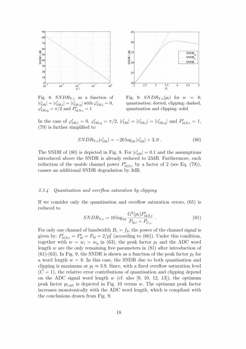
3.3.3 Crosstalk of LO carriers to the RF input ports of the mixers
In this section, the impact of crosstalk from the LO mixer input ports to theRF input of the mixers is considered separately. This kind of crosstalk causesa DC-offset at the DCR-ADI output. Hence, we best consider a channel c thatis allocated about f = 0. Deleting all other error sources, (65) becomes
SNDRY,c(c′
OS,i, ϕ′
OS,i, c′
OS,q, ϕ′
OS,q) = 10 log10
4P ′
id,S,c
c′2OS,i cos2 ϕ′
OS,i + c′2OS,q sin2 ϕ′
OS,q
.
(79)
17
10−4 10−3 10−2 10−1 1000
10
20
30
40
50
60
70
80
90
|c´|
SND
R /
dB
Fig. 8. SNDRY,c as a function of|c′OS| = |c′OS,i| = |c′OS,q| with ϕ′
OS,i = 0,ϕ′
OS,q = π/2 and P ′
id,S,c = 1
2 2.5 3 3.5 4 4.5 520
25
30
35
40
45
pf
SND
R /
dB SNDRQ
SNDRC
SNDR
Fig. 9. SNDRY,c(pf) for w = 8;quantisation: dotted, clipping: dashed,quantisation and clipping: solid
In the case of ϕ′
OS,i = 0, ϕ′
OS,q = π/2, |c′OS| = |c′OS,i| = |c′OS,q| and P ′
id,S,c = 1,(79) is further simplified to
SNDRY,c(c′
OS) = −20 log10 |c′OS| + 3, 0 . (80)
The SNDR of (80) is depicted in Fig. 8. For |c′OS| = 0.1 and the assumptionsintroduced above the SNDR is already reduced to 23dB. Furthermore, eachreduction of the usable channel power P ′
id,S,c by a factor of 2 (see Eq. (79)),causes an additional SNDR degradation by 3dB.
3.3.4 Quantisation and overflow saturation by clipping
If we consider only the quantisation and overflow saturation errors, (65) isreduced to
SNDRY,c = 10 log10
G2(pf)P′
id,S,c
PQ,c + PC,c
. (81)
For only one channel of bandwidth Bc = fS, the power of the channel signal isgiven by: P ′
id,S,c = P ′
id = Pid = 2/p2f (according to (60)). Under this condition,
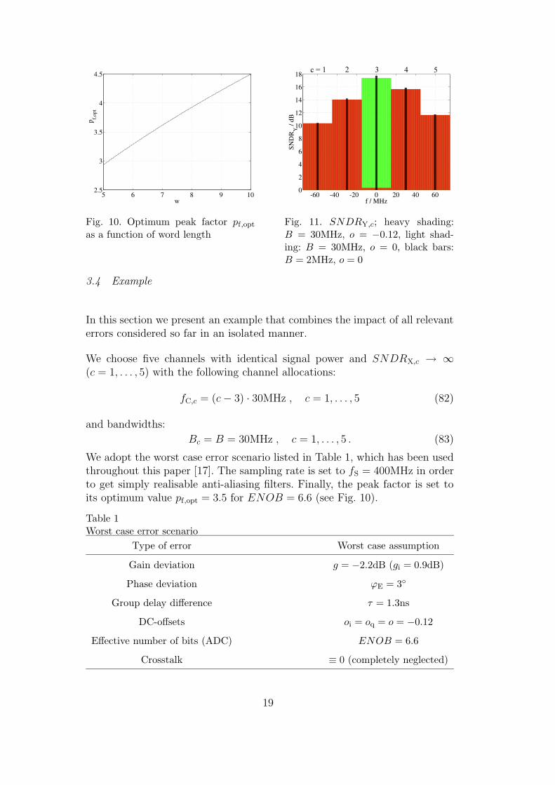
together with w = wi = wq in (63), the peak factor pf and the ADC wordlength w are the only remaining free parameters in (81) after introduction of(61)-(63). In Fig. 9, the SNDR is shown as a function of the peak factor pf fora word length w = 8. In this case, the SNDR due to both quantisation andclipping is maximum at pf ≈ 3.9. Since, with a fixed overflow saturation level(C = 1), the relative error contributions of quantisation and clipping dependon the ADC signal word length w (cf. also [9, 10, 12, 13]), the optimumpeak factor pf,opt is depicted in Fig. 10 versus w. The optimum peak factorincreases monotonically with the ADC word length, which is compliant withthe conclusions drawn from Fig. 9.
18
5 6 7 8 9 102.5
3
3.5
4
4.5
w
p f,opt
Fig. 10. Optimum peak factor pf,opt
as a function of word length
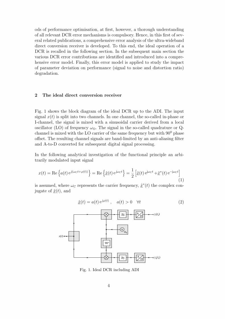
c = 1 2 3 4 5
Fig. 11. SNDRY,c; heavy shading:B = 30MHz, o = −0.12, light shad-ing: B = 30MHz, o = 0, black bars:B = 2MHz, o = 0
3.4 Example
In this section we present an example that combines the impact of all relevanterrors considered so far in an isolated manner.
We choose five channels with identical signal power and SNDRX,c → ∞(c = 1, . . . , 5) with the following channel allocations:
fC,c = (c − 3) · 30MHz , c = 1, . . . , 5 (82)
and bandwidths:
Bc = B = 30MHz , c = 1, . . . , 5 . (83)
We adopt the worst case error scenario listed in Table 1, which has been usedthroughout this paper [17]. The sampling rate is set to fS = 400MHz in orderto get simply realisable anti-aliasing filters. Finally, the peak factor is set toits optimum value pf,opt = 3.5 for ENOB = 6.6 (see Fig. 10).
Table 1Worst case error scenario
Type of error Worst case assumption
Gain deviation g = −2.2dB (gi = 0.9dB)
Phase deviation ϕE = 3
Group delay difference τ = 1.3ns
DC-offsets oi = oq = o = −0.12
Effective number of bits (ADC) ENOB = 6.6
Crosstalk ≡ 0 (completely neglected)
19
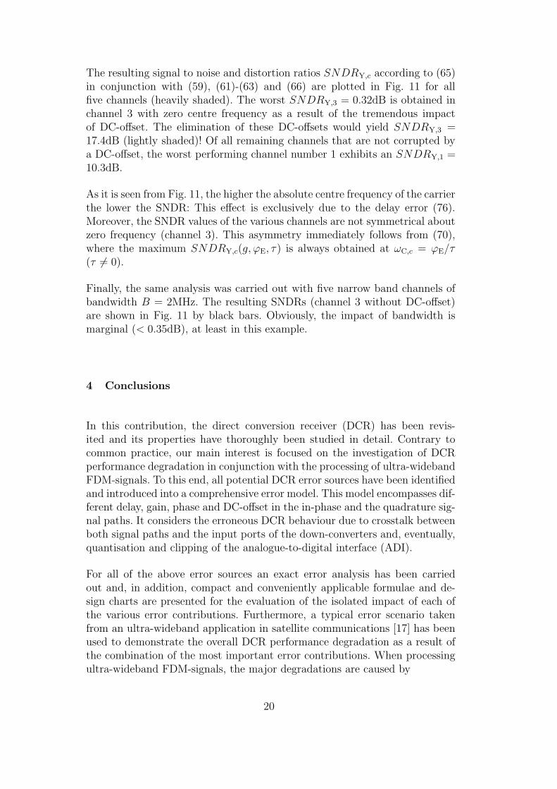
The resulting signal to noise and distortion ratios SNDRY,c according to (65)in conjunction with (59), (61)-(63) and (66) are plotted in Fig. 11 for allfive channels (heavily shaded). The worst SNDRY,3 = 0.32dB is obtained inchannel 3 with zero centre frequency as a result of the tremendous impactof DC-offset. The elimination of these DC-offsets would yield SNDRY,3 =17.4dB (lightly shaded)! Of all remaining channels that are not corrupted bya DC-offset, the worst performing channel number 1 exhibits an SNDRY,1 =10.3dB.
As it is seen from Fig. 11, the higher the absolute centre frequency of the carrierthe lower the SNDR: This effect is exclusively due to the delay error (76).Moreover, the SNDR values of the various channels are not symmetrical aboutzero frequency (channel 3). This asymmetry immediately follows from (70),where the maximum SNDRY,c(g, ϕE, τ) is always obtained at ωC,c = ϕE/τ(τ 6= 0).
Finally, the same analysis was carried out with five narrow band channels ofbandwidth B = 2MHz. The resulting SNDRs (channel 3 without DC-offset)are shown in Fig. 11 by black bars. Obviously, the impact of bandwidth ismarginal (< 0.35dB), at least in this example.
4 Conclusions
In this contribution, the direct conversion receiver (DCR) has been revis-ited and its properties have thoroughly been studied in detail. Contrary tocommon practice, our main interest is focused on the investigation of DCRperformance degradation in conjunction with the processing of ultra-widebandFDM-signals. To this end, all potential DCR error sources have been identifiedand introduced into a comprehensive error model. This model encompasses dif-ferent delay, gain, phase and DC-offset in the in-phase and the quadrature sig-nal paths. It considers the erroneous DCR behaviour due to crosstalk betweenboth signal paths and the input ports of the down-converters and, eventually,quantisation and clipping of the analogue-to-digital interface (ADI).
For all of the above error sources an exact error analysis has been carriedout and, in addition, compact and conveniently applicable formulae and de-sign charts are presented for the evaluation of the isolated impact of each ofthe various error contributions. Furthermore, a typical error scenario takenfrom an ultra-wideband application in satellite communications [17] has beenused to demonstrate the overall DCR performance degradation as a result ofthe combination of the most important error contributions. When processingultra-wideband FDM-signals, the major degradations are caused by
20
(1) delay differences between in-phase and quadrature path that, due to theirfrequency dependence, are most pronounced in edge channels,
(2) DC-offsets that, however, heavily impair the channel centred about zerofrequency only, and
(3) I- and Q-channel gain differences.
Each of these three error sources introduces, on its own, a performance degra-dation such that error correction measures are compulsive. In contrast, allother error contributions are of minor influence.
Meanwhile, our research in DCR error correction has been started by suitablemodification and supplementing the DCR error model introduced in section3. In particular, we are presently studying measures to reduce the impact ofDC-offset [7, 16, 19b], and investigate approaches to diminish delay [16, 18],gain [1, 4, 5, 14, 16, 19b, 22, 32, 33], and phase [1, 4, 5, 14, 19b, 22, 32, 33]errors including adaptive methods [4, 5, 14, 32, 33]. Results, to be verified byanalysis and simulation, will be reported as available.
References
[1] U. Bolliger, W. Vollenweider, Verfahren zum Korrigieren von Amplituden-und Phasenfehlern in einem Direct-Conversion-Empfanger und Empfanger zumDurchfuhren des Verfahrens, German patent DE 39 38 671 A1, 1990.
[2] J. Brakensiek, R. Wittmann, M. Darianian, Software defined radio technologyfor multistandard terminals, Proc. 2nd Karlsruhe Workshop on Software Radios,Karlsruhe, Germany, 20-21 March 2002, pp. 87-92.
[3] E. Buracchini, The software radio concept, IEEE Communications Magazine38 (9) (September 2000) 138-143.
[4] E. Cetin, I. Kale, R. C. S. Morling, Adaptive compensation of analog front-endI/Q mismatches in digital receivers, IEEE Int. Symp. on Circuits and Systems,Sydney, Australia, 6-9 May 2001, vol. IV, pp. 370-373.
[5] E. Cetin, I. Kale, R. C. S. Morling, Correction of transmitter gain and phaseerrors at the receiver, IEEE Int. Symp. on Circuits and Systems, Phoenix, USA,26-29 May 2002, vol. IV, pp. 109-112.
[6] Y. Dong, Ein neues Verfahren zur Messung der Eigenschaften schwachnichtlinearer Systeme, Doctoral Dissertation, Universitat Erlangen, Germany,1990.
[7] J.-E. Eklund, F. Gustafsson, Digital offset compensation of time-interleavedADC using random chopper sampling, IEEE Int. Symp. on Circuits andSystems, Geneva, Switzerland, 28-31 May 2000, vol. III, pp. 447-450.
21
[8] G. Garofalo, X. Manfroid, Personal communication, Europ. Space Agency,Noordwijk, Netherlands, 2002.
[9] T. Gebauer, H. G. Gockler, Teilnehmerindividuelle adaptive Strahlformung furden satellitengestutzten Mobilfunk, ANT Nachrichtentechnische Berichte 10(August 1993) 82-92.
[10] T. Gebauer, H. G. Gockler, Channel-individual adaptive beamformingfor mobile satellite communications, IEEE Journal on Selected Areas inCommunications 13 (2) (February 1995) 439-448.
[11] H. G. Gockler, H. Eyssele, Study of on-board digital FDM-demultiplexingfor mobile SCPC satellite communications (parts I & II), Europ. Trans.Telecommunic. 3 (1) (January-February 1992) 7-30.
[12] H. G. Gockler, T. Gebauer, Model-based simulation of a class of digitalFDM-demultiplexers in beamforming environment, Intern. Conf. Dig. Satell.Communic. (ICDSC-9), Kopenhagen, Danmark, May 1992, vol. A, pp. 311-318.
[13] H. G. Gockler, T. Gebauer, A digital FDM-demultiplexer for beamformingenvironment, IOS Press, Space Communications 10 (1992) 197-205.
[14] A. W. Gunst, G. W. Kant, Application of digital wide band mismatchcalibration to an I/Q receiver, IEEE Int. Symp. on Circuits and Systems,Phoenix, USA, 26-29 May 2002, vol. III, pp. 484-487.
[15] M. Gustavsson, J. J. Wikner, N. N. Tan, CMOS data converters forcommunications, Kluwer, Dordrecht, 2000.
[16] L. Haring, Verbesserung der Eigenschaften von Zeitmultiplex-A/D-Schnittstellen mit Verfahren der digitalen Signalverarbeitung, Master Thesis,Ruhr-Universitat Bochum, Germany, 2001.
[17] B. Hespeler, S. Kull, Personal communication, Tesat-Spacecom GmbH,Backnang, Germany, 2002.
[18] J. Huawen, E. K. F. Lee, A digital-background calibration technique forminimizing timing-error effects in time-interleaved ADC’s, IEEE Trans. CircuitsSyst. II 47 (7) (July 2000) 603-613.
[19a] F. Jehring, H.-J. Jentschel, W. Kluge, F.-M. Krause, Direktuberlagerungsemp-fanger - Realisierung mit digitaler Signalverarbeitung, Nachrichtentech.,Elektron. 43 (3) (1993) 142-148.
[19b] F. Jehring, H.-J. Jentschel, W. Kluge, F.-M. Krause, Direktuberlagerungsemp-fanger - Realisierung mit digitaler Signalverarbeitung (Teil 2), Nachrichtentech.,Elektron. 43 (4) (1993) 177-181.
[20] F. Jondral, R. Machauer, A. Wiesler, Software Radio, Schlembach, Weil derStadt, 2002.
[21] K. D. Kammeyer, K. Kroschel, Digitale Signalverarbeitung, Teubner, Stuttgart,1998.
22
[22] W. Kluge, F. Jehring, F.-M. Krause, Verfahren und Vorrichtung zur Korrekturder Phasen- und Amplitudenfehler bei direktmischenden Empfangseinrich-tungen, German patent DE 42 38 543 C1, 1994.
[23] H. Kopmann, Ansatze zur Verbesserung der Eigenschaften von A/D-Schnittstellen, Technical Report, Ruhr-Universitat Bochum, Germany, 2000.
[24] T. I. Laakso, A. Tarczynski, N. P. Murphy, V. Valimaki, Polynomial filteringapproach to reconstruction and noise reduction of nonuniformly sampledsignals, Signal Processing 80 (4) (April 2000) 567-575.
[25] L. Maurer, System design, simulation and specification of a UMTS compliantRF receiver front-end, Doctoral Dissertation, Johannes Kepler Universitat Linz,Austria, 2001.
[26] W. Namgoong, T. H. Meng, Direct-conversion RF receiver design, IEEE Trans.Commun. 49 (3) (March 2001) 518-529.
[27] C. T. Peach, W. Law, D. R. Beck, W. J. Helms, D. J. Allstot, Matchingconsiderations in I/Q A/D converter pairs, IEEE Int. Symp. on Circuits andSystems, Phoenix, USA, 26-29 May 2002, vol. III, pp. 145-148.
[28] B. Pregardier, Schnelle Folge / Halte-Verstarker und ihre Anwendung inmehrstufigen Analog / Digital-Umsetzern fur Auflosungen bis 10 bit, DoctoralDissertation, Ruhr-Universitat Bochum, Germany, 1996.
[29] S. Roome, Analysis of quadrature detectors using complex envelope notation,Proc. IEE 136 (2) (April 1989) 95-100.
[30] H. W. Schußler, Digitale Signalverarbeitung 1, Springer, Berlin / Heidelberg,1994.
[31] H. W. Schußler, P. Mohringer, P. Steffen, On partly digital anti-aliasing filters,Archiv fur Elektronik und Ubertragungstechnik 9 (1982) 349-355.
[32] M. Valkama, Advanced I/Q signal processing for wideband receivers: Modelsand algorithms, Doctoral Dissertation, Tampere University of Technology,Tampere, Finland, 2001.
[33] M. Valkama, M. Renfors, Digital I/Q imbalance compensation in directconversion receivers, Proc. 2nd Karlsruhe Workshop on Software Radios,Karlsruhe, Germany, 20-21 March 2002, pp. 51-56.
[34] R. H. Walden, Analog-to-digital converter survey and analysis, IEEE Journalon Selected Areas in Communications 17 (4) (April 1999) 539-550.
[35] R. H. Walden, Performance trends for analog-to-digital converters, IEEECommunications Magazine 37 (2) (February 1999) 96-101.
23