compact size 3d magnetometer based on magnetoresistive sensors · compact size 3d magnetometer...
TRANSCRIPT
Compact size 3D magnetometer based on magnetoresistive sensors
Gabriel Antonio Nunes FarinhaUnder supervision of Prof. Susana Freitas
Instituto de Engenharia de Sistemas e Computadores, Microsistemas e NanotecnologiasUniversidade Tecnica de Lisboa, Lisbon, Portugal
This thesis presents the optimization of magnetoresistive sensors working by tunnel effect, clas-sified as state of the art in magnetic detection, with the advantage of been produced with smalldimensions, aiming the development of a magnetometer.
Stacks were deposited to produce this type of sensors, with amorphous barriers of AlOx. Strategiesas shape anisotropy were used to allow the linearization of the sensors, achieving for top pinned aTMR of 35%, and for bottom pinned configurations a TMR of 29%, with both free and pinned layerscomposed by (CoFe)B. The incorporation of NiFe on the free layer allowed to have sensors with0.05 mT of coercivity and TMR of 29%. The detectivity values obtained were 120 nT/
√Hz at low
frequencies and 20 nT/√Hz at high frequencies, with a noise density characterized by an Hooge
parameter of 4.86× 10⁻⁹ µm2.The final device is a magnetometer, which is capable of measuring magnetic fields in three spatial
dimensions, with a sensitivity of 5.6 mV/mT in the range of -10 mT and +10 mT, composed by 4single sensors assembled on Wheatstone bridge configuration for each dimension.
Keywords: Magnetic tunnel junctions, 3D magnetometer, shape anisotropy linearization, AlOxbarrier, Wheatstone bridge.
I. INTRODUCTION
Magnetic sensors are extremely important nowadays.They are widely used, being integrated in many devices,such as mobile phones, medical devices and navigationtools. This thesis explores further applications, aimingdeveloping/characterizing magnetic sensors to be imple-mented in, for example, spatial aircrafts. A magnetome-ter capable of measuring magnetic fields in the 3 dimen-sions of space, working with magnetoresistive sensorsbased on tunnel effect, is the goal of this thesis.
Magnetic tunnel junctions (MTJs) were first reportedat low temperatures by Julliere [1]. This device is, inthe most basic model, composed by two ferromagneticlayers with a non-magnetic spacer between them. Thisspacer is an insulating layer, which force the electronsto tunnel between the two ferromagnets. One of the fer-romagnetic layers will remain fixed for fields at which theother layer will rotate, being one the reference layer andthe other the free layer. Tunneling Magnetoresistance(TMR) is the variation of resistance of the device withthe rotation of the free layer under the influence of anexternal magnetic field.
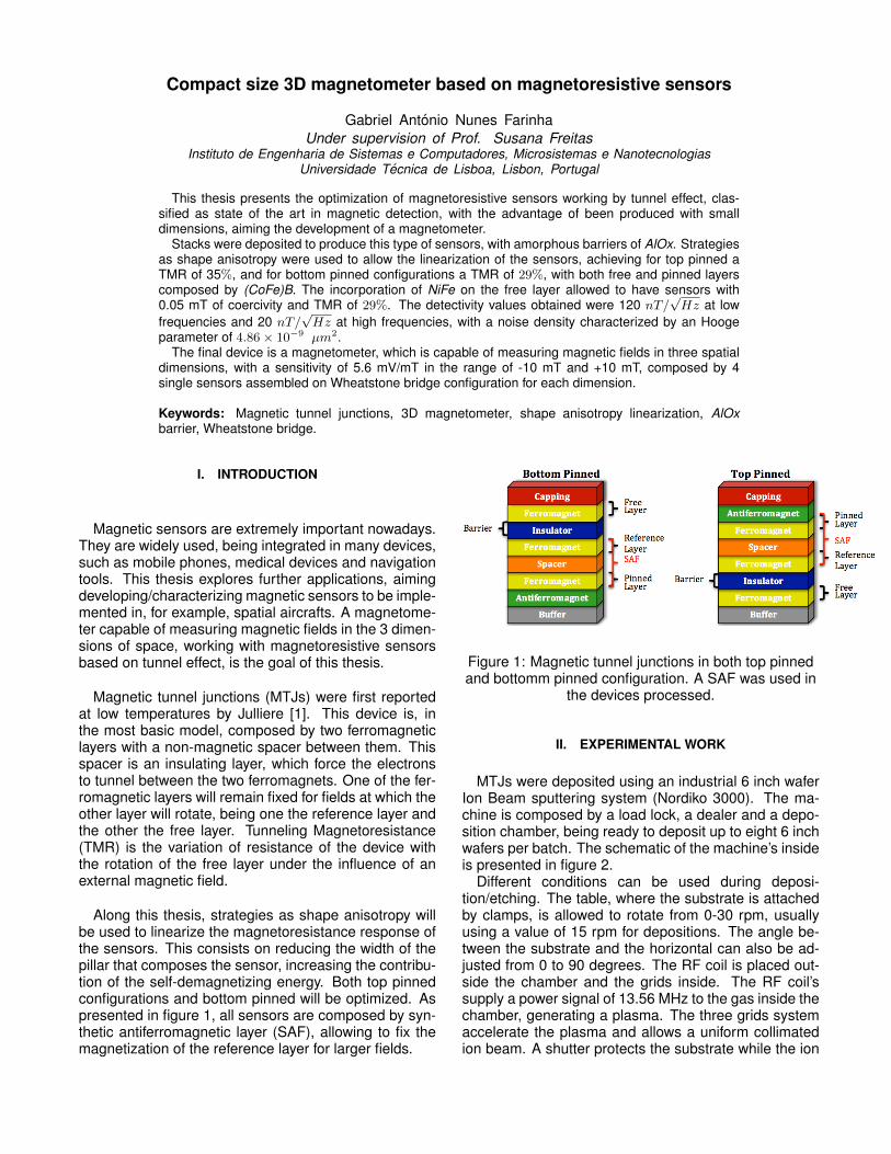
Along this thesis, strategies as shape anisotropy willbe used to linearize the magnetoresistance response ofthe sensors. This consists on reducing the width of thepillar that composes the sensor, increasing the contribu-tion of the self-demagnetizing energy. Both top pinnedconfigurations and bottom pinned will be optimized. Aspresented in figure 1, all sensors are composed by syn-thetic antiferromagnetic layer (SAF), allowing to fix themagnetization of the reference layer for larger fields.
Figure 1: Magnetic tunnel junctions in both top pinnedand bottomm pinned configuration. A SAF was used in
the devices processed.
II. EXPERIMENTAL WORK
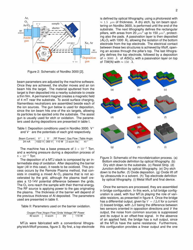
MTJs were deposited using an industrial 6 inch waferIon Beam sputtering system (Nordiko 3000). The ma-chine is composed by a load lock, a dealer and a depo-sition chamber, being ready to deposit up to eight 6 inchwafers per batch. The schematic of the machine’s insideis presented in figure 2.
Different conditions can be used during deposi-tion/etching. The table, where the substrate is attachedby clamps, is allowed to rotate from 0-30 rpm, usuallyusing a value of 15 rpm for depositions. The angle be-tween the substrate and the horizontal can also be ad-justed from 0 to 90 degrees. The RF coil is placed out-side the chamber and the grids inside. The RF coil’ssupply a power signal of 13.56 MHz to the gas inside thechamber, generating a plasma. The three grids systemaccelerate the plasma and allows a uniform collimatedion beam. A shutter protects the substrate while the ion
2
Figure 2: Schematic of Nordiko 3000 [2].
beam parameters are adjusted by the machine software.Once they are achieved, the shutter moves and an ionbeam hits the target. The material sputtered from thetarget is then deposited into a nearby substrate to createa thin film. A permanent magnet creates a magnetic fieldof 4 mT near the substrate. To avoid surface charging,filamentless neutralizers are assembled beside each ofthe ion sources. The gun below is used for deposition,since the ion beam hits one of the six targets, allowingits particles to be ejected onto the substrate. The assistgun is usually used for etch or oxidation. The parame-ters used during depositions are presented in table I.
Table I: Deposition conditions used in Nordiko 3000. V+
and V− are the potentials of each grid respectively.
Beam Current V+ V− RF Power Gas Flow Table Angle24 mA 1022 V -300 V 110 W 2 sccm Xe 80
The machine has a base pressure of 3 × 10⁻⁷ Torr,and a working pressure during a deposition process of8× 10−5 Torr.
The deposition of a MTJ stack is composed by an in-termediate step of oxidation. After depositing the barrierlayer (Al in this case), it needs to be oxidized. This pro-cess occurs by the Remote Plasma method, that con-sists in creating a mixed Ar-O2 plasma that is not ac-celerated by the grid, although the plasma itself cre-ates a 12-14V potential difference between the grids.The O2 ions reach the sample with their thermal energy.The RF source is applying power to the gas originatingthe plasma. The thickness of the barrier will depend ofthe previous thickness of Al deposited. The parametersused are presented in table II.
Table II: Parameters used on the barrier oxidation.
Oxygen Flow Argon Flow Grids Voltage RF Power40 sccm 4 sccm 0V 110 W
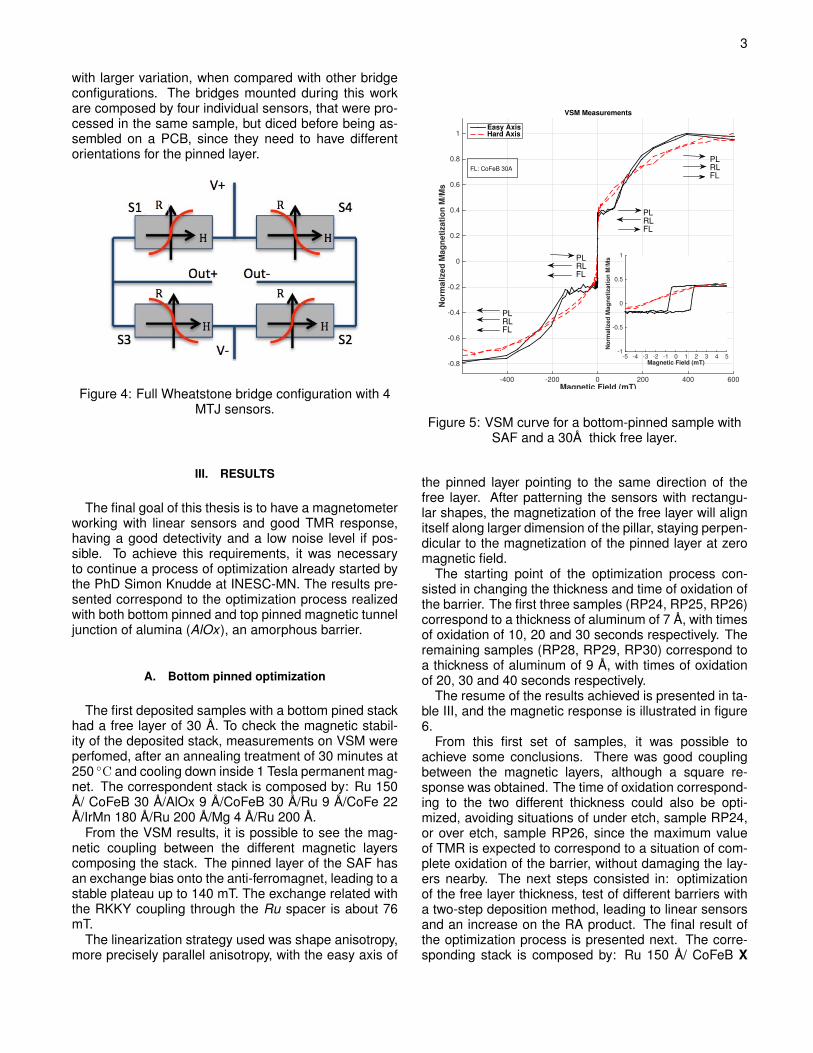
MTJs were fabricated with a conventional lithogra-phy/etch/liftoff process, figure 3. By first, a top electrode
is defined by optical lithography, using a photoresist with≈ 1.5 µm of thickness. A dry etch, by ion beam sput-tering on Nordiko 3600, is performed until the end of thesubstrate. The next lithography defines the rectangularpillars, with areas from 20 µm2 up to 150 µm2, protect-ing also the pads. A passivation layer is then deposited(Al2O2 with 1000 A), allowing the isolation of the bottomelectrode from the top electrode. The electrical contactbetween these two structures is achieved by liftoff, open-ing an access through the pillar’s top. The last lithogra-phy defines the top electrode, followed by a depositionof ≈ 3000 A of AlSiCu, with a passivation layer on topof TiW(N) with ≈ 150 A.
(a) (b) (c)
(d) (e) (f)
(g) (h) (i)
Figure 3: Schematic of the microfabrication process. (a)Bottom electrode definition by optical lithography. (b)Dry etch down to the substrate. (c) Resist Strip. (d)
Junction definition by optical lithography. (e) Dry etchdown to the buffer. (f) Oxide deposition. (g) Oxide lift offby ultrasounds in a solvent. (h) Top electrode definitionby optical lithography. (i) Metal liftoff and final device.
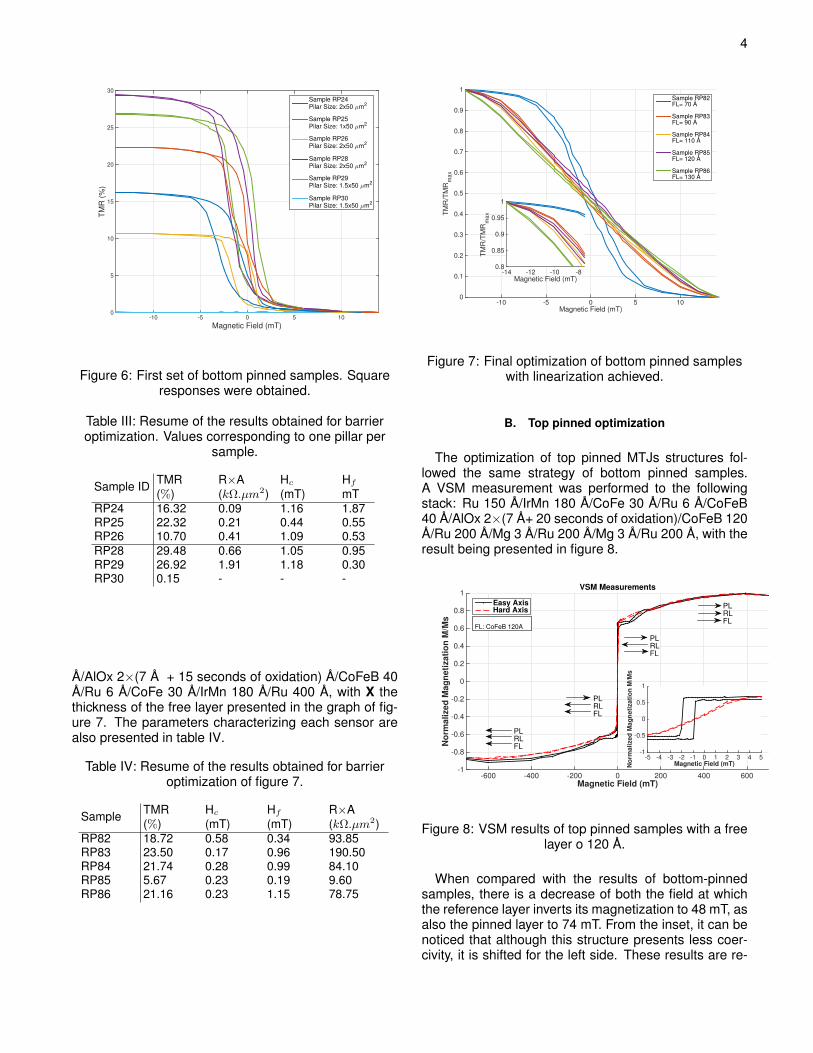
Once the sensors are processed, they are assembledin bridge configuration. In this work, a full bridge config-uration is used, with four MTJs playing the role of vari-able resistors, as presented in figure 4. Once the bridgehas a differential output, given by V = I∆R for a current(I) biased bridge, with ∆R being the difference betweentwo sensors oriented in opposition directions and V theoutput, the noise from common sources is suppressedand its output is an offset-free signal. In the absenceof an applied field, the bridge has a null output, sinceall the MTJs have the same resistance. Furthermore,this configuration provides a linear output and the one
3
with larger variation, when compared with other bridgeconfigurations. The bridges mounted during this workare composed by four individual sensors, that were pro-cessed in the same sample, but diced before being as-sembled on a PCB, since they need to have differentorientations for the pinned layer.
Figure 4: Full Wheatstone bridge configuration with 4MTJ sensors.
III. RESULTS
The final goal of this thesis is to have a magnetometerworking with linear sensors and good TMR response,having a good detectivity and a low noise level if pos-sible. To achieve this requirements, it was necessaryto continue a process of optimization already started bythe PhD Simon Knudde at INESC-MN. The results pre-sented correspond to the optimization process realizedwith both bottom pinned and top pinned magnetic tunneljunction of alumina (AlOx), an amorphous barrier.
A. Bottom pinned optimization
The first deposited samples with a bottom pined stackhad a free layer of 30 A. To check the magnetic stabil-ity of the deposited stack, measurements on VSM wereperfomed, after an annealing treatment of 30 minutes at250 C and cooling down inside 1 Tesla permanent mag-net. The correspondent stack is composed by: Ru 150A/ CoFeB 30 A/AlOx 9 A/CoFeB 30 A/Ru 9 A/CoFe 22A/IrMn 180 A/Ru 200 A/Mg 4 A/Ru 200 A.
From the VSM results, it is possible to see the mag-netic coupling between the different magnetic layerscomposing the stack. The pinned layer of the SAF hasan exchange bias onto the anti-ferromagnet, leading to astable plateau up to 140 mT. The exchange related withthe RKKY coupling through the Ru spacer is about 76mT.
The linearization strategy used was shape anisotropy,more precisely parallel anisotropy, with the easy axis of
Magnetic Field (mT)-400 -200 0 200 400 600
No
rmalized
Mag
neti
zati
on
M/M
s
-0.8
-0.6
-0.4
-0.2
0
0.2
0.4
0.6
0.8
1
VSM Measurements
Easy AxisHard Axis
Magnetic Field (mT)-5 -4 -3 -2 -1 0 1 2 3 4 5
No
rmali
ze
d M
ag
neti
zati
on
M/M
s
-1
-0.5
0
0.5
1
PL
RL
FL
PL
RL
FL
PL
RL
FL
PL
RL
FL
FL: CoFeB 30A
Figure 5: VSM curve for a bottom-pinned sample withSAF and a 30A thick free layer.
the pinned layer pointing to the same direction of thefree layer. After patterning the sensors with rectangu-lar shapes, the magnetization of the free layer will alignitself along larger dimension of the pillar, staying perpen-dicular to the magnetization of the pinned layer at zeromagnetic field.
The starting point of the optimization process con-sisted in changing the thickness and time of oxidation ofthe barrier. The first three samples (RP24, RP25, RP26)correspond to a thickness of aluminum of 7 A, with timesof oxidation of 10, 20 and 30 seconds respectively. Theremaining samples (RP28, RP29, RP30) correspond toa thickness of aluminum of 9 A, with times of oxidationof 20, 30 and 40 seconds respectively.
The resume of the results achieved is presented in ta-ble III, and the magnetic response is illustrated in figure6.
From this first set of samples, it was possible toachieve some conclusions. There was good couplingbetween the magnetic layers, although a square re-sponse was obtained. The time of oxidation correspond-ing to the two different thickness could also be opti-mized, avoiding situations of under etch, sample RP24,or over etch, sample RP26, since the maximum valueof TMR is expected to correspond to a situation of com-plete oxidation of the barrier, without damaging the lay-ers nearby. The next steps consisted in: optimizationof the free layer thickness, test of different barriers witha two-step deposition method, leading to linear sensorsand an increase on the RA product. The final result ofthe optimization process is presented next. The corre-sponding stack is composed by: Ru 150 A/ CoFeB X
4
Magnetic Field (mT)-10 -5 0 5 10
TM
R (
%)
0
5
10
15
20
25
30
Sample RP24Pilar Size: 2x50 µm2
Sample RP25Pilar Size: 1x50 µm2
Sample RP26Pilar Size: 2x50 µm2
Sample RP28Pilar Size: 2x50 µm2
Sample RP29Pilar Size: 1.5x50 µm2
Sample RP30Pilar Size: 1.5x50 µm2
Figure 6: First set of bottom pinned samples. Squareresponses were obtained.
Table III: Resume of the results obtained for barrieroptimization. Values corresponding to one pillar per
sample.
Sample ID TMR R×A Hc Hf
(%) (kΩ.µm2) (mT) mTRP24 16.32 0.09 1.16 1.87RP25 22.32 0.21 0.44 0.55RP26 10.70 0.41 1.09 0.53RP28 29.48 0.66 1.05 0.95RP29 26.92 1.91 1.18 0.30RP30 0.15 - - -
A/AlOx 2×(7 A + 15 seconds of oxidation) A/CoFeB 40A/Ru 6 A/CoFe 30 A/IrMn 180 A/Ru 400 A, with X thethickness of the free layer presented in the graph of fig-ure 7. The parameters characterizing each sensor arealso presented in table IV.
Table IV: Resume of the results obtained for barrieroptimization of figure 7.
Sample TMR Hc Hf R×A(%) (mT) (mT) (kΩ.µm2)
RP82 18.72 0.58 0.34 93.85RP83 23.50 0.17 0.96 190.50RP84 21.74 0.28 0.99 84.10RP85 5.67 0.23 0.19 9.60RP86 21.16 0.23 1.15 78.75
Magnetic Field (mT)-10 -5 0 5 10
TM
R/T
MR
max
0
0.1
0.2
0.3
0.4
0.5
0.6
0.7
0.8
0.9
1Sample RP82FL= 70 Å
Sample RP83FL= 90 Å
Sample RP84FL= 110 Å
Sample RP85FL= 120 Å
Sample RP86FL= 130 Å
Magnetic Field (mT)-14 -12 -10 -8
TM
R/T
MR
max
0.8
0.85
0.9
0.95
1
Figure 7: Final optimization of bottom pinned sampleswith linearization achieved.
B. Top pinned optimization
The optimization of top pinned MTJs structures fol-lowed the same strategy of bottom pinned samples.A VSM measurement was performed to the followingstack: Ru 150 A/IrMn 180 A/CoFe 30 A/Ru 6 A/CoFeB40 A/AlOx 2×(7 A+ 20 seconds of oxidation)/CoFeB 120A/Ru 200 A/Mg 3 A/Ru 200 A/Mg 3 A/Ru 200 A, with theresult being presented in figure 8.
Magnetic Field (mT)-600 -400 -200 0 200 400 600
No
rma
lize
d M
ag
ne
tiza
tio
n M
/Ms
-1
-0.8
-0.6
-0.4
-0.2
0
0.2
0.4
0.6
0.8
1VSM Measurements
Easy AxisHard Axis
Magnetic Field (mT)-5 -4 -3 -2 -1 0 1 2 3 4 5
No
rma
lize
d M
ag
ne
tiza
tio
n M
/Ms
-1
-0.5
0
0.5
1
PL
RL
FL
PL
RL
FL
PL
RL
FL
PL
RL
FLFL: CoFeB 120A
Figure 8: VSM results of top pinned samples with a freelayer o 120 A.
When compared with the results of bottom-pinnedsamples, there is a decrease of both the field at whichthe reference layer inverts its magnetization to 48 mT, asalso the pinned layer to 74 mT. From the inset, it can benoticed that although this structure presents less coer-civity, it is shifted for the left side. These results are re-
5
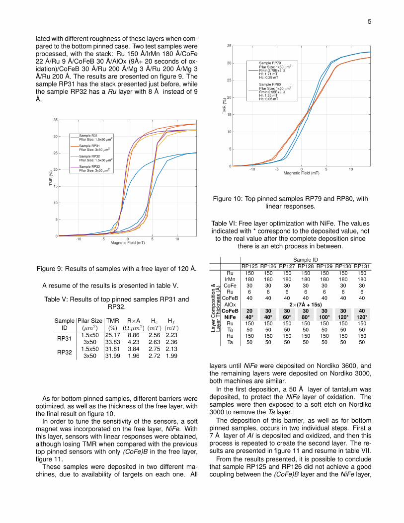
lated with different roughness of these layers when com-pared to the bottom pinned case. Two test samples wereprocessed, with the stack: Ru 150 A/IrMn 180 A/CoFe22 A/Ru 9 A/CoFeB 30 A/AlOx (9A+ 20 seconds of ox-idation)/CoFeB 30 A/Ru 200 A/Mg 3 A/Ru 200 A/Mg 3A/Ru 200 A. The results are presented on figure 9. Thesample RP31 has the stack presented just before, whilethe sample RP32 has a Ru layer with 8 A instead of 9A.
Magnetic Field (mT)-10 -5 0 5 10
TM
R (
%)
0
5
10
15
20
25
30
35
Sample R31Pilar Size: 1.5x50 µm2
Sample RP31Pilar Size: 3x50 µm2
Sample RP32Pilar Size: 1.5x50 µm2
Sample RP32Pilar Size: 3x50 µm2
Figure 9: Results of samples with a free layer of 120 A.
A resume of the results is presented in table V.
Table V: Results of top pinned samples RP31 andRP32.
Sample Pilar Size TMR R×A Hc Hf
ID (µm2) (%) (Ω.µm2) (mT ) (mT )
RP31 1.5x50 25.17 8.86 2.56 2.233x50 33.83 4.23 2.63 2.36
RP32 1.5x50 31.81 3.84 2.75 2.133x50 31.99 1.96 2.72 1.99
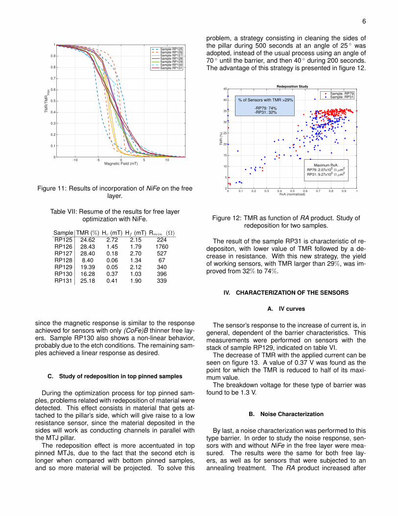
As for bottom pinned samples, different barriers wereoptimized, as well as the thickness of the free layer, withthe final result on figure 10.
In order to tune the sensitivity of the sensors, a softmagnet was incorporated on the free layer, NiFe. Withthis layer, sensors with linear responses were obtained,although losing TMR when compared with the previoustop pinned sensors with only (CoFe)B in the free layer,figure 11.
These samples were deposited in two different ma-chines, due to availability of targets on each one. All
Magnetic Field (mT)-10 -5 0 5 10
TM
R (
%)
0
5
10
15
20
25
30
35
Sample RP79Pilar Size: 1x50 µm2
Rmin:2.78E+2 ΩHf: 1.71 mTHc: 0.29 mT
Sample RP80Pilar Size: 1x50 µm2
Rmin:2.95E+2 ΩHf: 1.35 mTHc: 0.05 mT
Figure 10: Top pinned samples RP79 and RP80, withlinear responses.
Table VI: Free layer optimization with NiFe. The valuesindicated with * correspond to the deposited value, not
to the real value after the complete deposition sincethere is an etch process in between.
Sample IDRP125 RP126 RP127 RP128 RP129 RP130 RP131
Laye
rCom
posi
tion
&La
yerT
hick
ness
(A)
Ru 150 150 150 150 150 150 150IrMn 180 180 180 180 180 180 180CoFe 30 30 30 30 30 30 30
Ru 6 6 6 6 6 6 6CoFeB 40 40 40 40 40 40 40AlOx 2×(7A + 15s)
CoFeB 20 30 30 30 30 30 40NiFe 40* 40* 60* 80* 100* 120* 120*Ru 150 150 150 150 150 150 150Ta 50 50 50 50 50 50 50Ru 150 150 150 150 150 150 150Ta 50 50 50 50 50 50 50
layers until NiFe were deposited on Nordiko 3600, andthe remaining layers were deposited on Nordiko 3000,both machines are similar.
In the first deposition, a 50 A layer of tantalum wasdeposited, to protect the NiFe layer of oxidation. Thesamples were then exposed to a soft etch on Nordiko3000 to remove the Ta layer.
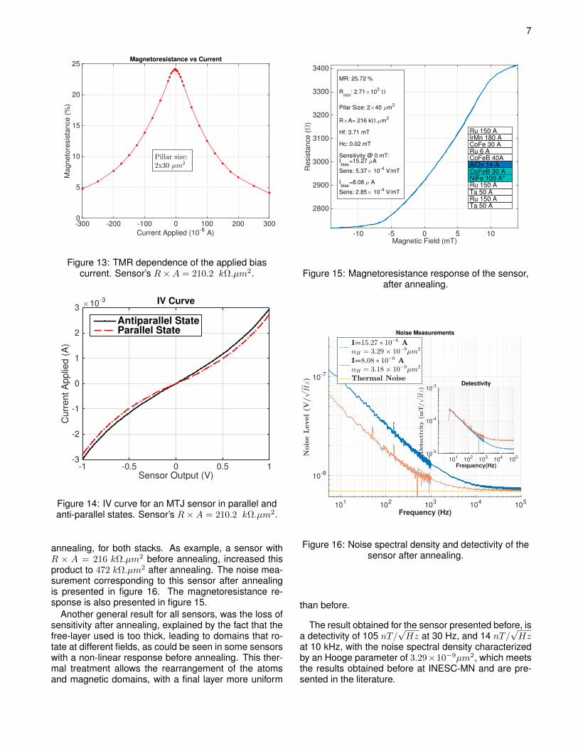
The deposition of this barrier, as well as for bottompinned samples, occurs in two individual steps. First a7 A layer of Al is deposited and oxidized, and then thisprocess is repeated to create the second layer. The re-sults are presented in figure 11 and resume in table VII.
From the results presented, it is possible to concludethat sample RP125 and RP126 did not achieve a goodcoupling between the (CoFe)B layer and the NiFe layer,
6
Magnetic Field (mT)-10 -5 0 5 10
TM
R/T
MR
ma
x
0
0.1
0.2
0.3
0.4
0.5
0.6
0.7
0.8
0.9
1
Sample RP125Sample RP126Sample RP127Sample RP128Sample RP129Sample RP130Sample RP131
Figure 11: Results of incorporation of NiFe on the freelayer.
Table VII: Resume of the results for free layeroptimization with NiFe.
Sample TMR (%) Hc (mT) Hf (mT) Rmin (Ω)RP125 24.62 2.72 2.15 224RP126 28.43 1.45 1.79 1760RP127 28.40 0.18 2.70 527RP128 8.40 0.06 1.34 67RP129 19.39 0.05 2.12 340RP130 16.28 0.37 1.03 396RP131 25.18 0.41 1.90 339
since the magnetic response is similar to the responseachieved for sensors with only (CoFe)B thinner free lay-ers. Sample RP130 also shows a non-linear behavior,probably due to the etch conditions. The remaining sam-ples achieved a linear response as desired.
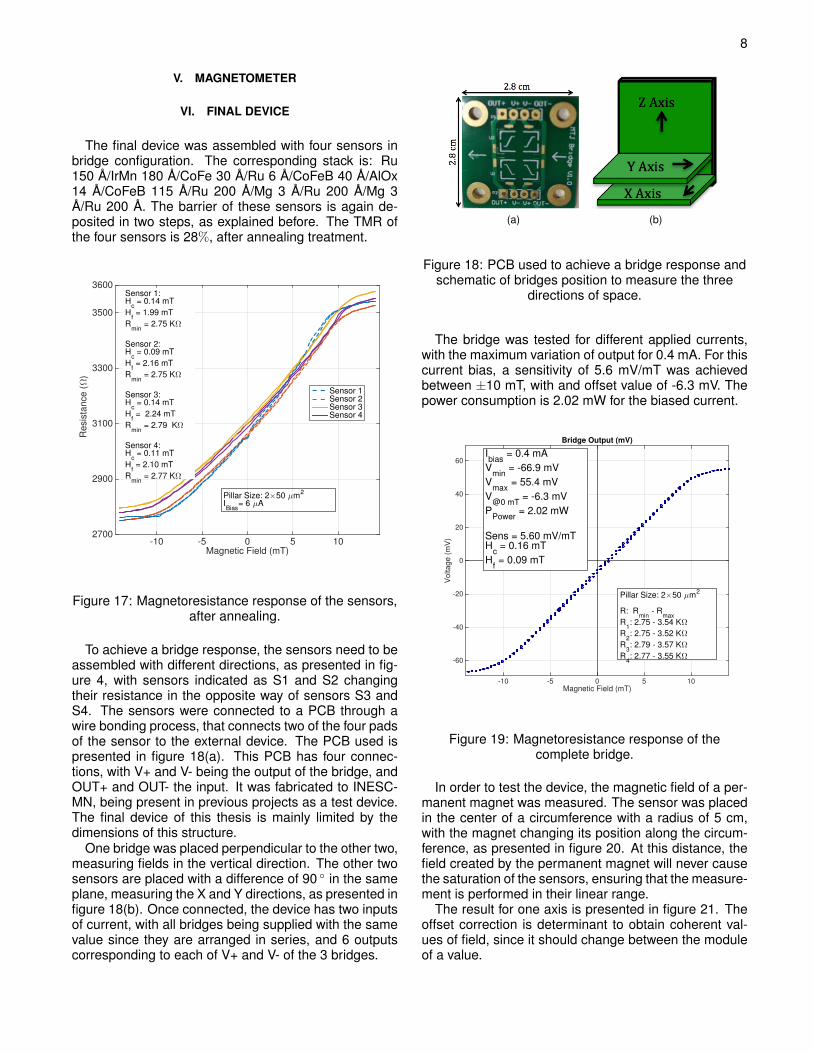
C. Study of redeposition in top pinned samples
During the optimization process for top pinned sam-ples, problems related with redeposition of material weredetected. This effect consists in material that gets at-tached to the pillar’s side, which will give raise to a lowresistance sensor, since the material deposited in thesides will work as conducting channels in parallel withthe MTJ pillar.
The redeposition effect is more accentuated in toppinned MTJs, due to the fact that the second etch islonger when compared with bottom pinned samples,and so more material will be projected. To solve this
problem, a strategy consisting in cleaning the sides ofthe pillar during 500 seconds at an angle of 25 wasadopted, instead of the usual process using an angle of70 until the barrier, and then 40 during 200 seconds.The advantage of this strategy is presented in figure 12.
RxA (normalized)0 0.1 0.2 0.3 0.4 0.5 0.6 0.7 0.8 0.9 1
TM
R (
%)
0
5
10
15
20
25
30
35
40
45Redeposition Study
Sample: RP79Sample: RP31
% of Sensors with TMR >29%
-RP79: 74%-RP31: 32%
Maximum RxA:
RP79: 2.07x10⁵ Ω.µm
2
RP31: 9.27x10² Ω.µm
2
Figure 12: TMR as function of RA product. Study ofredeposition for two samples.
The result of the sample RP31 is characteristic of re-depositon, with lower value of TMR followed by a de-crease in resistance. With this new strategy, the yieldof working sensors, with TMR larger than 29%, was im-proved from 32% to 74%.
IV. CHARACTERIZATION OF THE SENSORS
A. IV curves
The sensor’s response to the increase of current is, ingeneral, dependent of the barrier characteristics. Thismeasurements were performed on sensors with thestack of sample RP129, indicated on table VI.
The decrease of TMR with the applied current can beseen on figure 13. A value of 0.37 V was found as thepoint for which the TMR is reduced to half of its maxi-mum value.
The breakdown voltage for these type of barrier wasfound to be 1.3 V.
B. Noise Characterization
By last, a noise characterization was performed to thistype barrier. In order to study the noise response, sen-sors with and without NiFe in the free layer were mea-sured. The results were the same for both free lay-ers, as well as for sensors that were subjected to anannealing treatment. The RA product increased after
7
Current Applied (10-6
A)
-300 -200 -100 0 100 200 300
Ma
gn
eto
resis
tan
ce
(%
)
0
5
10
15
20
25Magnetoresistance vs Current
Pillar size:
2x30 µm2
Figure 13: TMR dependence of the applied biascurrent. Sensor’s R×A = 210.2 kΩ.µm2.
Sensor Output (V)-1 -0.5 0 0.5 1
Curr
ent A
pplie
d (
A)
×10-3
-3
-2
-1
0
1
2
3IV Curve
Antiparallel StateParallel State
Figure 14: IV curve for an MTJ sensor in parallel andanti-parallel states. Sensor’s R×A = 210.2 kΩ.µm2.
annealing, for both stacks. As example, a sensor withR × A = 216 kΩ.µm2 before annealing, increased thisproduct to 472 kΩ.µm2 after annealing. The noise mea-surement corresponding to this sensor after annealingis presented in figure 16. The magnetoresistance re-sponse is also presented in figure 15.
Another general result for all sensors, was the loss ofsensitivity after annealing, explained by the fact that thefree-layer used is too thick, leading to domains that ro-tate at different fields, as could be seen in some sensorswith a non-linear response before annealing. This ther-mal treatment allows the rearrangement of the atomsand magnetic domains, with a final layer more uniform
Magnetic Field (mT)-10 -5 0 5 10
Re
sist
an
ce (Ω
)
2800
2900
3000
3100
3200
3300
3400
Ta 50 ARu 150 ATa 50 ARu 150 ANiFe 100 A*CoFeB 30 AAlOx 14 ACoFeB 40ARu 6 ACoFe 30 AIrMn 180 ARu 150 A
MR: 25.72 %
Rmin
: 2.71×10³ Ω
Pilar Size: 2×40 µm2
R×A= 216 kΩ.µm2
Hf: 3.71 mT
Hc: 0.02 mT
Sensitivity @ 0 mT:Ibias
=15.27 µA
Sens: 5.37× 10⁻⁴ V/mT
Ibias
=8.08 µ A
Sens: 2.85× 10⁻⁴ V/mT
Figure 15: Magnetoresistance response of the sensor,after annealing.
Frequency (Hz)10
110
210
310
410
5
NoiseLevel(V
/√
Hz)
10-8
10-7
Noise Measurements
I=15.27 ∗ 10−6 A
αH = 3.29× 10⁻⁹µm
2
I=8.08 ∗ 10−6 A
αH = 3.18× 10⁻⁹µm
2
Thermal Noise
Frequency(Hz)10
110
210
310
410
5
Detectivity(m
T/√
Hz)
10-5
10-4
10-3
Detectivity
Figure 16: Noise spectral density and detectivity of thesensor after annealing.
than before.
The result obtained for the sensor presented before, isa detectivity of 105 nT/
√Hz at 30 Hz, and 14 nT/
√Hz
at 10 kHz, with the noise spectral density characterizedby an Hooge parameter of 3.29×10⁻⁹µm2, which meetsthe results obtained before at INESC-MN and are pre-sented in the literature.
8
V. MAGNETOMETER
VI. FINAL DEVICE
The final device was assembled with four sensors inbridge configuration. The corresponding stack is: Ru150 A/IrMn 180 A/CoFe 30 A/Ru 6 A/CoFeB 40 A/AlOx14 A/CoFeB 115 A/Ru 200 A/Mg 3 A/Ru 200 A/Mg 3A/Ru 200 A. The barrier of these sensors is again de-posited in two steps, as explained before. The TMR ofthe four sensors is 28%, after annealing treatment.
Magnetic Field (mT)-10 -5 0 5 10
Re
sis
tan
ce
(Ω
)
2700
2900
3100
3300
3500
3600
Sensor 1Sensor 2Sensor 3Sensor 4
Pillar Size: 2×50 µm2
IBias
= 6 µA
Sensor 1:H
c = 0.14 mT
Hf = 1.99 mT
Rmin
= 2.75 KΩ
Sensor 2:H
c = 0.09 mT
Hf = 2.16 mT
Rmin
= 2.75 KΩ
Sensor 3:H
c = 0.14 mT
Hf = 2.24 mT
Rmin
= 2.79 KΩ
Sensor 4:H
c = 0.11 mT
Hf = 2.10 mT
Rmin
= 2.77 KΩ
Figure 17: Magnetoresistance response of the sensors,after annealing.
To achieve a bridge response, the sensors need to beassembled with different directions, as presented in fig-ure 4, with sensors indicated as S1 and S2 changingtheir resistance in the opposite way of sensors S3 andS4. The sensors were connected to a PCB through awire bonding process, that connects two of the four padsof the sensor to the external device. The PCB used ispresented in figure 18(a). This PCB has four connec-tions, with V+ and V- being the output of the bridge, andOUT+ and OUT- the input. It was fabricated to INESC-MN, being present in previous projects as a test device.The final device of this thesis is mainly limited by thedimensions of this structure.
One bridge was placed perpendicular to the other two,measuring fields in the vertical direction. The other twosensors are placed with a difference of 90 in the sameplane, measuring the X and Y directions, as presented infigure 18(b). Once connected, the device has two inputsof current, with all bridges being supplied with the samevalue since they are arranged in series, and 6 outputscorresponding to each of V+ and V- of the 3 bridges.
(a) (b)
Figure 18: PCB used to achieve a bridge response andschematic of bridges position to measure the three
directions of space.
The bridge was tested for different applied currents,with the maximum variation of output for 0.4 mA. For thiscurrent bias, a sensitivity of 5.6 mV/mT was achievedbetween ±10 mT, with and offset value of -6.3 mV. Thepower consumption is 2.02 mW for the biased current.
Magnetic Field (mT)-10 -5 0 5 10
Vo
ltag
e (
mV
)
-60
-40
-20
0
20
40
60
Bridge Output (mV)
Pillar Size: 2×50 µm2
R: Rmin
- Rmax
R1: 2.75 - 3.54 KΩ
R2: 2.75 - 3.52 KΩ
R3: 2.79 - 3.57 KΩ
R4: 2.77 - 3.55 KΩ
Ibias
= 0.4 mA
Vmin
= -66.9 mV
Vmax
= 55.4 mV
V@0 mT
= -6.3 mV
PPower
= 2.02 mW
Sens = 5.60 mV/mTH
c = 0.16 mT
Hf = 0.09 mT
Figure 19: Magnetoresistance response of thecomplete bridge.
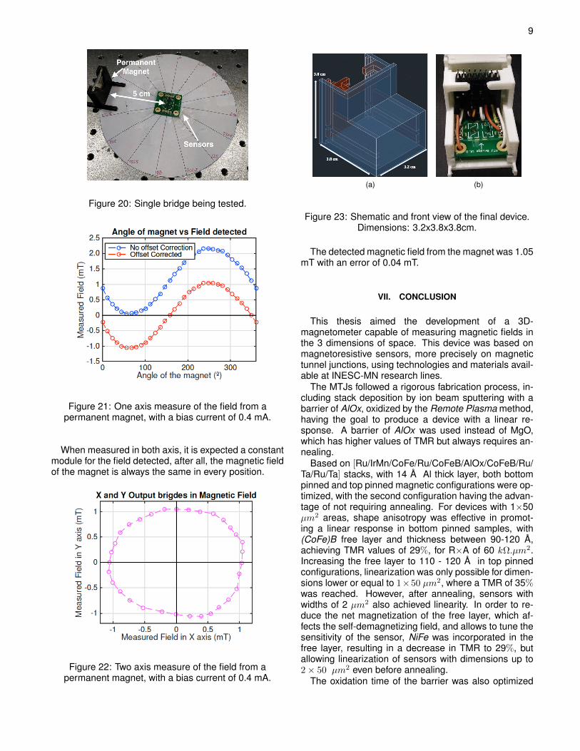
In order to test the device, the magnetic field of a per-manent magnet was measured. The sensor was placedin the center of a circumference with a radius of 5 cm,with the magnet changing its position along the circum-ference, as presented in figure 20. At this distance, thefield created by the permanent magnet will never causethe saturation of the sensors, ensuring that the measure-ment is performed in their linear range.
The result for one axis is presented in figure 21. Theoffset correction is determinant to obtain coherent val-ues of field, since it should change between the moduleof a value.
9
Figure 20: Single bridge being tested.
Figure 21: One axis measure of the field from apermanent magnet, with a bias current of 0.4 mA.
When measured in both axis, it is expected a constantmodule for the field detected, after all, the magnetic fieldof the magnet is always the same in every position.
Figure 22: Two axis measure of the field from apermanent magnet, with a bias current of 0.4 mA.
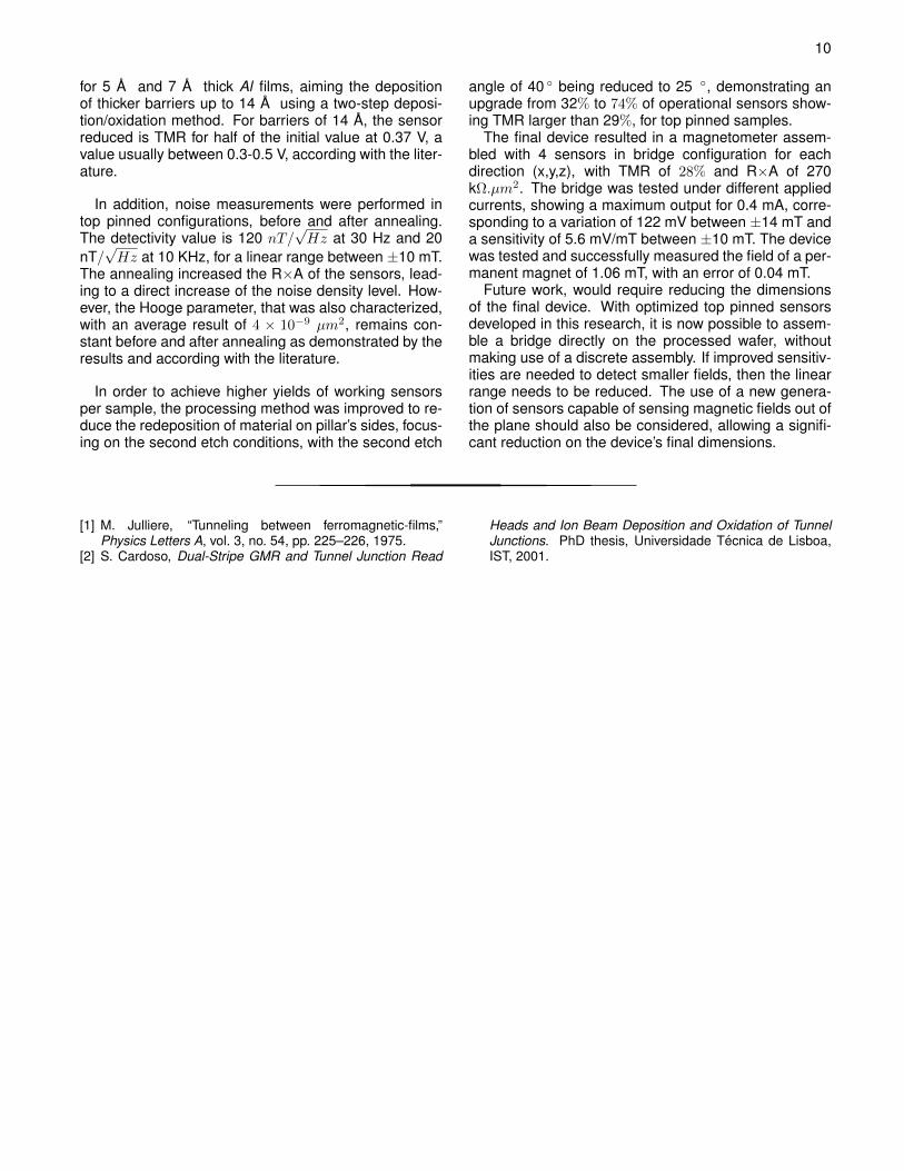
(a) (b)
Figure 23: Shematic and front view of the final device.Dimensions: 3.2x3.8x3.8cm.
The detected magnetic field from the magnet was 1.05mT with an error of 0.04 mT.
VII. CONCLUSION
This thesis aimed the development of a 3D-magnetometer capable of measuring magnetic fields inthe 3 dimensions of space. This device was based onmagnetoresistive sensors, more precisely on magnetictunnel junctions, using technologies and materials avail-able at INESC-MN research lines.
The MTJs followed a rigorous fabrication process, in-cluding stack deposition by ion beam sputtering with abarrier of AlOx, oxidized by the Remote Plasma method,having the goal to produce a device with a linear re-sponse. A barrier of AlOx was used instead of MgO,which has higher values of TMR but always requires an-nealing.
Based on [Ru/IrMn/CoFe/Ru/CoFeB/AlOx/CoFeB/Ru/Ta/Ru/Ta] stacks, with 14 A Al thick layer, both bottompinned and top pinned magnetic configurations were op-timized, with the second configuration having the advan-tage of not requiring annealing. For devices with 1×50µm2 areas, shape anisotropy was effective in promot-ing a linear response in bottom pinned samples, with(CoFe)B free layer and thickness between 90-120 A,achieving TMR values of 29%, for R×A of 60 kΩ.µm2.Increasing the free layer to 110 - 120 A in top pinnedconfigurations, linearization was only possible for dimen-sions lower or equal to 1×50 µm2, where a TMR of 35%was reached. However, after annealing, sensors withwidths of 2 µm2 also achieved linearity. In order to re-duce the net magnetization of the free layer, which af-fects the self-demagnetizing field, and allows to tune thesensitivity of the sensor, NiFe was incorporated in thefree layer, resulting in a decrease in TMR to 29%, butallowing linearization of sensors with dimensions up to2× 50 µm2 even before annealing.
The oxidation time of the barrier was also optimized
10
for 5 A and 7 A thick Al films, aiming the depositionof thicker barriers up to 14 A using a two-step deposi-tion/oxidation method. For barriers of 14 A, the sensorreduced is TMR for half of the initial value at 0.37 V, avalue usually between 0.3-0.5 V, according with the liter-ature.
In addition, noise measurements were performed intop pinned configurations, before and after annealing.The detectivity value is 120 nT/
√Hz at 30 Hz and 20
nT/√Hz at 10 KHz, for a linear range between ±10 mT.
The annealing increased the R×A of the sensors, lead-ing to a direct increase of the noise density level. How-ever, the Hooge parameter, that was also characterized,with an average result of 4 × 10⁻⁹ µm2, remains con-stant before and after annealing as demonstrated by theresults and according with the literature.
In order to achieve higher yields of working sensorsper sample, the processing method was improved to re-duce the redeposition of material on pillar’s sides, focus-ing on the second etch conditions, with the second etch
angle of 40 being reduced to 25 , demonstrating anupgrade from 32% to 74% of operational sensors show-ing TMR larger than 29%, for top pinned samples.
The final device resulted in a magnetometer assem-bled with 4 sensors in bridge configuration for eachdirection (x,y,z), with TMR of 28% and R×A of 270kΩ.µm2. The bridge was tested under different appliedcurrents, showing a maximum output for 0.4 mA, corre-sponding to a variation of 122 mV between ±14 mT anda sensitivity of 5.6 mV/mT between ±10 mT. The devicewas tested and successfully measured the field of a per-manent magnet of 1.06 mT, with an error of 0.04 mT.
Future work, would require reducing the dimensionsof the final device. With optimized top pinned sensorsdeveloped in this research, it is now possible to assem-ble a bridge directly on the processed wafer, withoutmaking use of a discrete assembly. If improved sensitiv-ities are needed to detect smaller fields, then the linearrange needs to be reduced. The use of a new genera-tion of sensors capable of sensing magnetic fields out ofthe plane should also be considered, allowing a signifi-cant reduction on the device’s final dimensions.
[1] M. Julliere, “Tunneling between ferromagnetic-films,”Physics Letters A, vol. 3, no. 54, pp. 225–226, 1975.
[2] S. Cardoso, Dual-Stripe GMR and Tunnel Junction Read
Heads and Ion Beam Deposition and Oxidation of TunnelJunctions. PhD thesis, Universidade Tecnica de Lisboa,IST, 2001.