commercial applications of nanotechnology · commercial applications of nanotechnology heli...
TRANSCRIPT

1
COMMERCIAL APPLICATIONS OF NANOTECHNOLOGYCOMMERCIAL APPLICATIONS OF NANOTECHNOLOGY
Heli JantunenUniversity of Oulu
Microelectronics and Materials Physics LaboratoriesEMPART Research Group of Infotech Oulu
Infotech “Day of Science” in Oulu, 11th of Nov., 2005
2
ITEMS TO BE DISCUSSEDITEMS TO BE DISCUSSED
• Current nanotechnology applications
• Future application in the world
• In Finland
• In Oulu area
Infotech “Day of Science” in Oulu, 11th of Nov., 2005

3
THE MOST FAMOUS NANOTECHNOLOGY APPLICATIONSTHE MOST FAMOUS NANOTECHNOLOGY APPLICATIONS
Infotech “Day of Science” in Oulu, 11th of Nov., 2005
The yellow- and red-colored stained glass on the rose window of Notre Dame Cathedral is made up of nanometer-size particles of silver and gold.
Dependence of colours obtained on particle size and the rose window at Notre Dame Cathedral, Paris. Haes et al., J. Fluorescence, July 2004.
MODERN APPLICATIONSMODERN APPLICATIONS: sensors, biological labels, OLEDs…
Evident Technologies, USA, produces commercial Quantum Dots with size < 10 nm for e.g. lightning, solar cell and biological markers applications http://www.evidenttech.com/
4
OTHER COMMERCIAL APPLICATIONS TODAYOTHER COMMERCIAL APPLICATIONS TODAY
Infotech “Day of Science” in Oulu, 11th of Nov., 2005
Mercedes M-classscratch-proof paint, nanoparticlesnanoparticles inpaint harden in paintshop oven
A three-fold improvement in scratch resistance
Wilson’s and Bobolat’s better tennis rackets with carbon nano tubes and strategic location of nano size silicon particles
10 time stiffer and extremely durable rackets

5
OTHER COMMERCIAL APPLICATIONS TODAYOTHER COMMERCIAL APPLICATIONS TODAY
Infotech “Day of Science” in Oulu, 11th of Nov., 2005
Lotus Effect® water-repellentselfself--cleaning shirtscleaning shirts - water repellent surface, dirt particles can hardly get a hold and can thus be removed by a rinse
(summer 2005, also glass, spray, paint)
L’Oreal Cosmetics’ Plenitude line contains nanocapsulatesnanocapsulates which active ingredients get tothe skin’s deeper layer
(130-600 um, tiny polymeric shell capable of guiding the active ingredients to the right place in the skin.
6
SiO2 gate oxide with 1.2 nm thickness (Intel)
Intel nano transistors with gate length from 50 nm to 15 nm
2003 IEDM2002
Prototype 2005
Prototype 2007
Prototype 2009
C. Block, Extending Moore’s Law with Nanotechnology, IntelCo., IR-TR-2003-5-CarolynBlock091803.pdf
INTEL NANO TRANSISTORSINTEL NANO TRANSISTORSIEDM2002, 2003
PROTOTYPE 2005
PROTOTYPE 2007
PROTOTYPE 2009

7
ON THE MARKETON THE MARKET• lasers modulators for telecommunication• computer peripherals (e.g. VCSEL = Vertical Cavity Surface Emitting
Laser)• sunscreens with nanoparticles• nanocatalyts• ”lab-on-chip” diagnostics, biomaterials• electronic displays (”intelligent ink on paper”)
COMMING SOONCOMMING SOON• friction resistant surfaces • harder –lighter – stronger materials • electronics components (smaller and more powerful memory devices)• ceramic membranes (filters)• fuel additives • paper-like displays, flexible circuitry and flexible solar cells• light, flexible, wearable electronics
OTHER COMMERCIAL APPLICATIONS TODAYOTHER COMMERCIAL APPLICATIONS TODAY
8
GLOBAL NANOTECHNOLOGY MARKET, 2002GLOBAL NANOTECHNOLOGY MARKET, 2002--20082008
http://www.bccresearch.com/nano/
28 %
17 %
9 %
6 %
9 %
31 %
Materiaalit
Elektroniikka
Kemikaalin valmistus
Ilmailu
Lääkkeet
Muut
YEAR 2015Scenario from 0,5 billion US$ to 2,0 billion US$
Materials
Electronics
Medicenes
Chemistry
Aviation
Others

9
Infotech “Day of Science” in Oulu, 11th of Nov., 2005
FACTS OF FINNISH NANOTECHNOLOGYFACTS OF FINNISH NANOTECHNOLOGY
The first Finnish nanotechnology programme NANONANO (1997-1999).The number of nanotechnology publicationspublications has increased steadily. Finland is the 26th in international comparison.1
Finnish nanotechnology patentspatents are still few.2
Several recognized nanotechnology competence networkscompetence networks exist.Between 300 and 500 people500 people work actively with nanotechnology. The first call of FinNano resulted 102 pre102 pre--proposalsproposals, total costs of over 91 M€.
1. Third European Report on Science & Technology Indicators, EC (2003)2. Tekes & VTT (2004)
NANOTECHNOLOGY IN TEKES (12.10.2005)NANOTECHNOLOGY IN TEKES (12.10.2005)
Projects contain nanotechnologyAll together 50 projects
approx. 20 company projectsapprox. 30 research projects9 proposals
10
Infotech “Day of Science” in Oulu, 11th of Nov., 2005
TEKESTEKES FinNanoFinNano ––PROGRAMMEPROGRAMME
Focus onFocus on• Innovative nanostructured materials• New solutions for nanoelectronics• Nanosensors and nanoactuators

TARGETS AND METHODS IN FINLAND
PARTICIPATING COMPANIES IN FINNANO
12
Infotech “Day of Science” in Oulu, 11th of Nov., 2005
The aim of the research programme is to increase nano-research networking nationally and internationally, and to prepare for future requirements of infrastructure and expertsInterdisciplinary nature of research is seen essential Preliminary thematic areas are:Preliminary thematic areas are:•• Directed SelfDirected Self--AssemblyAssembly•• Functionality in NanoscaleFunctionality in Nanoscale•• Properties of Single Nanoscale ObjectsProperties of Single Nanoscale Objects
The proposed duration is four years (2006-2009)Proposed volume is 10 million eurosProgramme Call is expected in November with DL in January 2006Programme Call is expected in November with DL in January 2006
NANOSCIENCE RESEARCH PROGRAMME OF THE NANOSCIENCE RESEARCH PROGRAMME OF THE ACADEMY OF FINLANDACADEMY OF FINLAND
13
Infotech “Day of Science” in Oulu, 11th of Nov., 2005
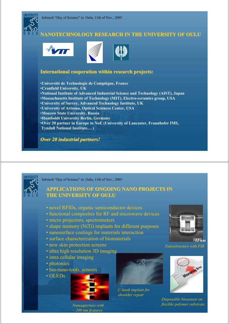
NANOTECHNOLOGY RESEARCH IN THE UNIVERSITY OF OULUNANOTECHNOLOGY RESEARCH IN THE UNIVERSITY OF OULU
International cooperation within research projects:International cooperation within research projects:
•Université de Technologie de Compiègne, France•Cranfield University, UK •National Institute of Advanced Industrial Science and Technology (AIST), Japan•Massachusetts Institute of Technology (MIT), Electro-ceramics group, USA•University of Surrey, Advanced Technology Institute, UK•University of Arizona, Optical Sciences Center, USA •Moscow State University, Russia•Humboldt University Berlin, Germany•Over 20 partner in Europe in NoE (University of Lancaster, Fraunhofer IMS, Tyndall National Institute,…)
Over 20 industrial partners!Over 20 industrial partners!
14
APPLICATIONS OF ONGOING NANO PROJECTS IN APPLICATIONS OF ONGOING NANO PROJECTS IN THE UNIVERSITY OF OULUTHE UNIVERSITY OF OULU
• novel RFIDs, organic semiconductor devices• functional composites for RF and microwave devices• micro projectors, spectrometers• shape memory (NiTi) implants for different purposes• nanosurface coatings for materials interaction• surface characterization of biomaterials• new skin protection screens• ultra high resolution 3D imaging• intra cellular imaging• photonics• bio-nano-tools, sensors• OLEDs
C-hook implant for shoulder repair
12 umNanostructure with FIB
Disposable biosensor on flexible polymer substrate.Nanoaperture with
~ 200 nm features
Infotech “Day of Science” in Oulu, 11th of Nov., 2005

15
Infotech “Day of Science” in Oulu, 11th of Nov., 2005
ACKNOWLEDGEMENTSACKNOWLEDGEMENTS
• Dr. Markku Lämsä, TEKES• Dr. Petri Ahonen, Academy of Finland• Dr. Pekka Koponen, Spinverse Consulting Oy• Dr. Laura Juvonen, Spinverse Consulting Oy• Prof. Osmo Hormi, Organic Chemistry• Prof. Timo Jämsä, Department of Medical Technology • Prof. Risto Myllyllä, Optoelectronics and Measurement Techniques Laboratory• Prof. Markku Moilanen, Optoelectronics and Measurement Techniques Laboratory• Dr. Jukka Hast, Optoelectronics and Measurement Techniques Laboratory• Dr. Krisztian Kordas, Microelectronics and Materials Physics Laboratories• Dr. Tao Hu, Microelectronics and Materials Physics Laboratories
•• Research Group of Research Group of NaperoNapero Project in VTT and Oulu UniversityProject in VTT and Oulu University
16
Infotech “Day of Science” in Oulu, 11th of Nov., 2005
NanotechnologyNanotechnology inin NorthernNorthern EuropeEuropeCongressCongress andand ExhibitionExhibition
Congress key themesCongress key themes
Nanoelectronics and Nanophotonics
Nanotechnology Instruments and Tools
Nanotechnology and Safety
NTNE 2006 16-18 May 2006Wanha Satama, Helsinki, Finland
Leading Nanotechnology Forum focusing on North European strengths
ExhibitionExhibition
Extensive exhibition in connection with the congress
FinNano Annual Seminar on 18 May
MoreMore informationinformation
www.nano.fi

17
MANY THANKS FOR YOUR ATTENTION!MANY THANKS FOR YOUR ATTENTION!
Heli Jantunen
Infotech “Day of Science” in Oulu, 11th of Nov., 2005