combining data remapping and voltage/frequency...
TRANSCRIPT
Combining Data Remapping and Voltage/Frequency Scaling of SecondLevel Memory for Energy Reduction in
Embedded Systems
Sudarshan K. Srinivasan, Jun Cheol Park and Vincent J. Mooney III
Georgia Institute of Technology{darshan, jcpark, mooney}@ece.gatech.edu
ESCODES 24 Sep. 2002Jun Cheol ParkGeorgia Institute of Technology 2
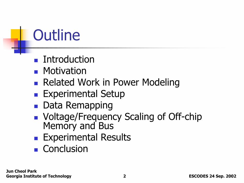
OutlineIntroductionMotivation Related Work in Power ModelingExperimental SetupData RemappingVoltage/Frequency Scaling of Off-chip Memory and BusExperimental ResultsConclusion
ESCODES 24 Sep. 2002Jun Cheol ParkGeorgia Institute of Technology 3
Introduction
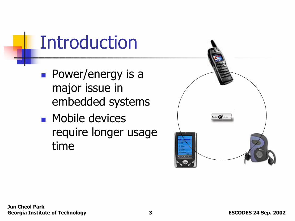
Power/energy is a major issue in embedded systemsMobile devices require longer usage time
ESCODES 24 Sep. 2002Jun Cheol ParkGeorgia Institute of Technology 4
Introduction (Cont.)
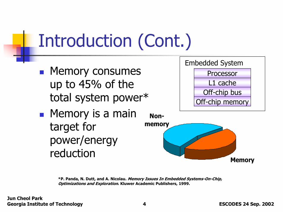
Memory consumes up to 45% of the total system power*Memory is a main target for power/energy reduction
Non-memory
Memory
*P. Panda, N. Dutt, and A. Nicolau. Memory Issues In Embedded Systems-On-Chip, Optimizations and Exploration. Kluwer Academic Publishers, 1999.
ProcessorEmbedded System
L1 cacheOff-chip bus
Off-chip memory
ESCODES 24 Sep. 2002Jun Cheol ParkGeorgia Institute of Technology 5
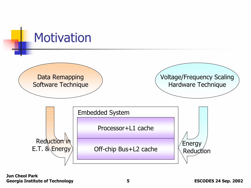
Motivation
Voltage/Frequency ScalingHardware Technique
Data RemappingSoftware Technique
Processor+L1 cache
EnergyReduction
Reduction in E.T. & Energy Off-chip Bus+L2 cache
Embedded System
ESCODES 24 Sep. 2002Jun Cheol ParkGeorgia Institute of Technology 6
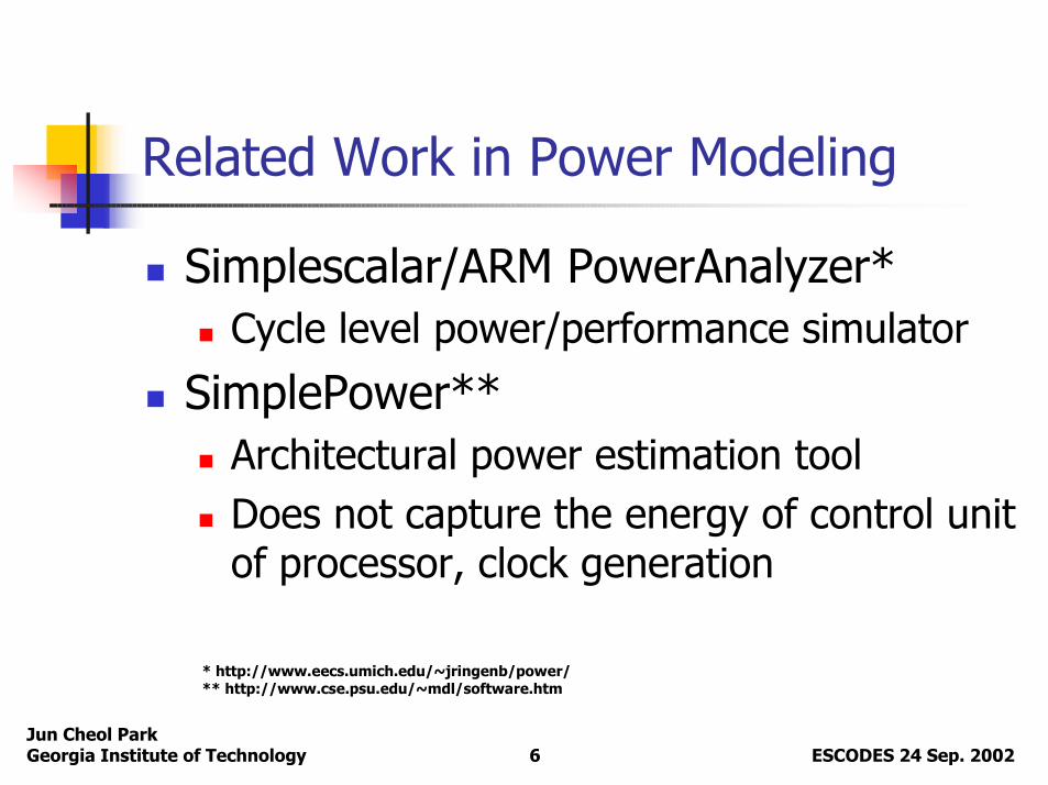
Related Work in Power Modeling
Simplescalar/ARM PowerAnalyzer*Cycle level power/performance simulator
SimplePower**Architectural power estimation tool Does not capture the energy of control unit of processor, clock generation
* http://www.eecs.umich.edu/~jringenb/power/** http://www.cse.psu.edu/~mdl/software.htm
ESCODES 24 Sep. 2002Jun Cheol ParkGeorgia Institute of Technology 7
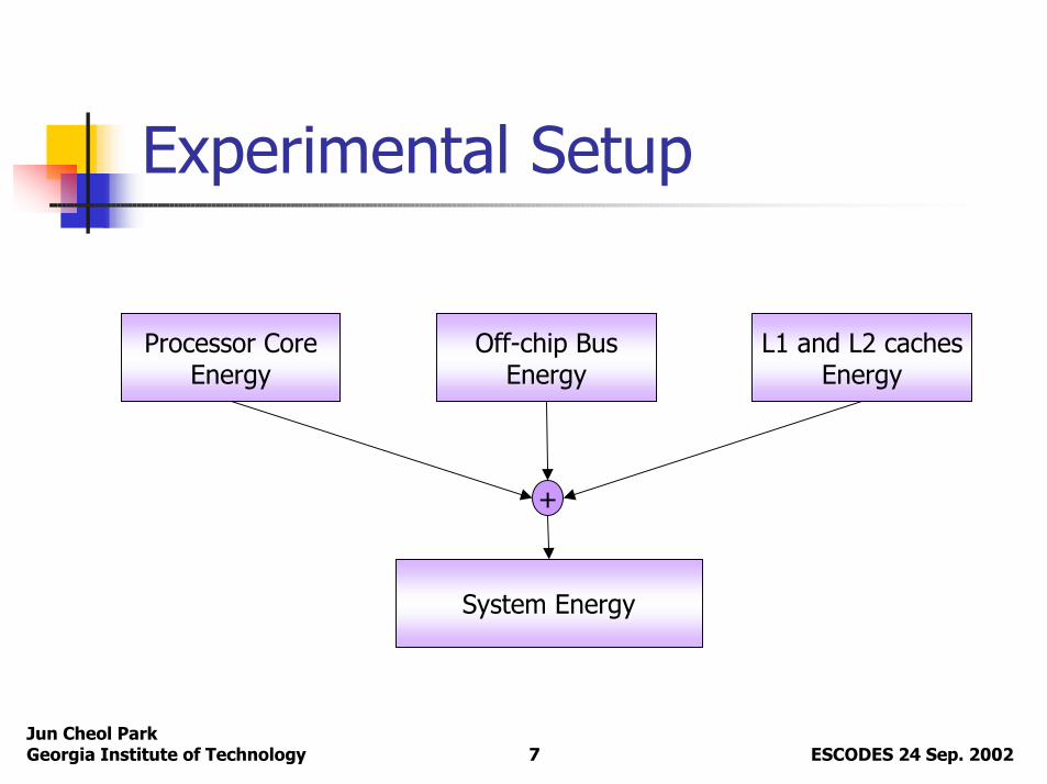
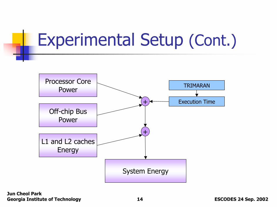
Experimental Setup
System Energy
Processor CoreEnergy
Off-chip BusEnergy
L1 and L2 cachesEnergy
+
ESCODES 24 Sep. 2002Jun Cheol ParkGeorgia Institute of Technology 8
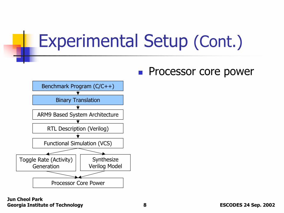
Experimental Setup (Cont.)
Binary Translation
ARM9 Based System Architecture
RTL Description (Verilog)
Functional Simulation (VCS)
Benchmark Program (C/C++)
Toggle Rate (Activity) Generation
Processor Core Power
Synthesize Verilog Model
Processor core power
ESCODES 24 Sep. 2002Jun Cheol ParkGeorgia Institute of Technology 9
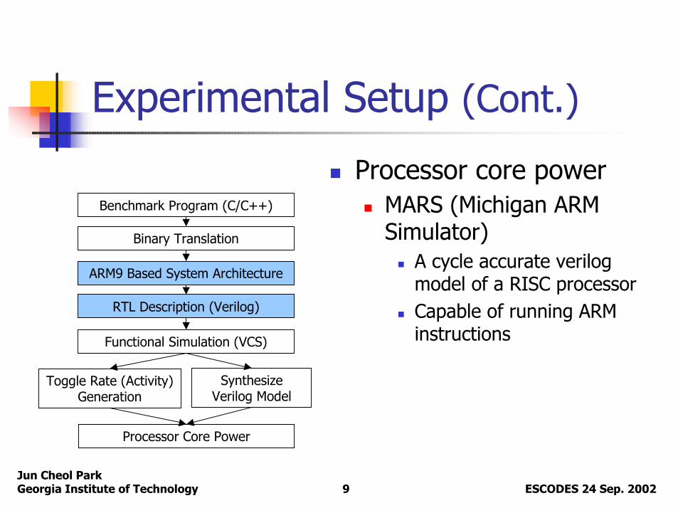
Experimental Setup (Cont.)
Processor core power MARS (Michigan ARM Simulator)
A cycle accurate verilogmodel of a RISC processor Capable of running ARM instructions
Binary Translation
ARM9 Based System Architecture
RTL Description (Verilog)
Functional Simulation (VCS)
Benchmark Program (C/C++)
Toggle Rate (Activity) Generation
Processor Core Power
Synthesize Verilog Model
ESCODES 24 Sep. 2002Jun Cheol ParkGeorgia Institute of Technology 10
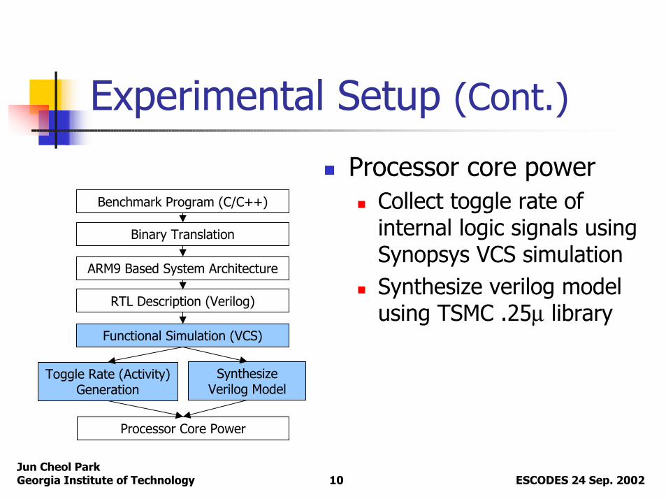
Experimental Setup (Cont.)
Processor core power Collect toggle rate of internal logic signals using Synopsys VCS simulationSynthesize verilog model using TSMC .25µ library
Binary Translation
ARM9 Based System Architecture
RTL Description (Verilog)
Functional Simulation (VCS)
Benchmark Program (C/C++)
Toggle Rate (Activity) Generation
Processor Core Power
Synthesize Verilog Model
ESCODES 24 Sep. 2002Jun Cheol ParkGeorgia Institute of Technology 11
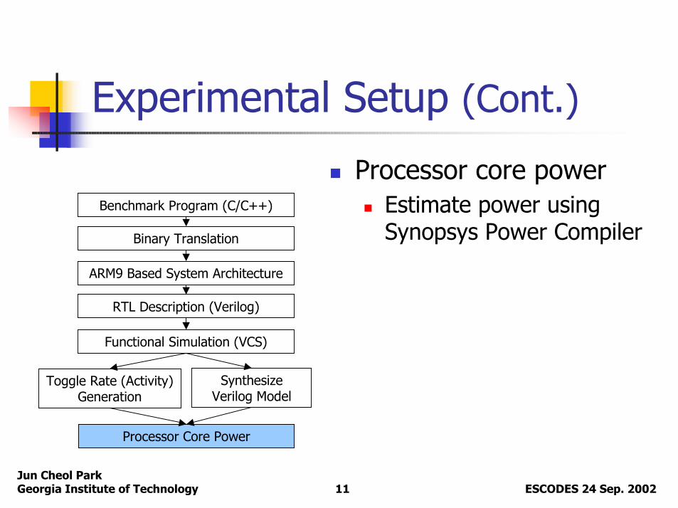
Experimental Setup (Cont.)
Processor core power Estimate power using Synopsys Power CompilerBinary Translation
ARM9 Based System Architecture
RTL Description (Verilog)
Functional Simulation (VCS)
Benchmark Program (C/C++)
Toggle Rate (Activity) Generation
Processor Core Power
Synthesize Verilog Model
ESCODES 24 Sep. 2002Jun Cheol ParkGeorgia Institute of Technology 12
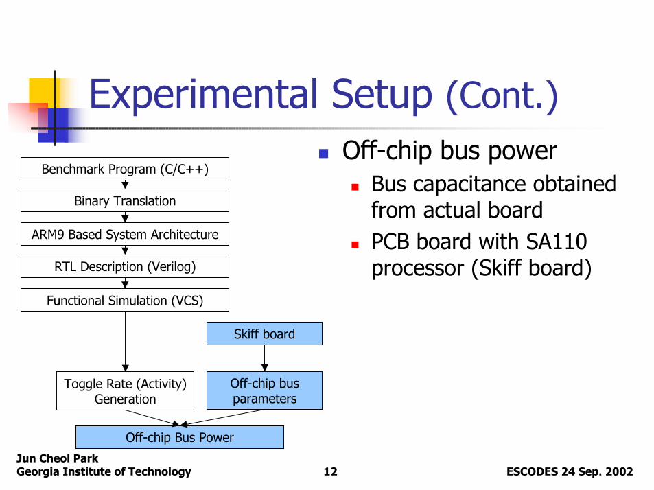
Experimental Setup (Cont.)Off-chip bus power
Bus capacitance obtained from actual boardPCB board with SA110 processor (Skiff board)
Binary Translation
ARM9 Based System Architecture
RTL Description (Verilog)
Functional Simulation (VCS)
Benchmark Program (C/C++)
Toggle Rate (Activity) Generation
Off-chip Bus Power
Off-chip bus parameters
Skiff board

ESCODES 24 Sep. 2002Jun Cheol ParkGeorgia Institute of Technology 13
L1 and L2 caches Energy
SMACSTRICEPS
Execution Time
Experimental Setup (Cont.)L1 and L2 caches energy
TRIMARAN*Integrated compilation and performance monitoring infrastructureARM-like processor simulatorTRICEPS
Generate ARM code
SMACS (Smart Memory and Cache Hierarchy Simulator)
cache activity statistics
Kamble and Ghose model**
TRIMARAN
Execution Statistics
*TRIMARAN http://www.trimaran.org**M. Kamble and K. Ghose ”Analytical energy dissipation models for low power caches,” Proceedings of the International Symposium on Low Power Electronics and Design, pp. 143-148, Aug. 1997.
ESCODES 24 Sep. 2002Jun Cheol ParkGeorgia Institute of Technology 14
Experimental Setup (Cont.)
System Energy
Processor CorePower
Off-chip BusPower
L1 and L2 cachesEnergy
+
Execution Time
TRIMARAN
+
ESCODES 24 Sep. 2002Jun Cheol ParkGeorgia Institute of Technology 15
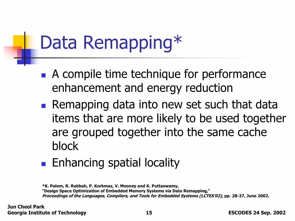
Data Remapping*
A compile time technique for performance enhancement and energy reductionRemapping data into new set such that data items that are more likely to be used together are grouped together into the same cache blockEnhancing spatial locality
*K. Palem, R. Rabbah, P. Korkmaz, V. Mooney and K. Puttaswamy, "Design Space Optimization of Embedded Memory Systems via Data Remapping," Proceedings of the Languages, Compilers, and Tools for Embedded Systems (LCTES’02), pp. 28-37, June 2002.
ESCODES 24 Sep. 2002Jun Cheol ParkGeorgia Institute of Technology 16
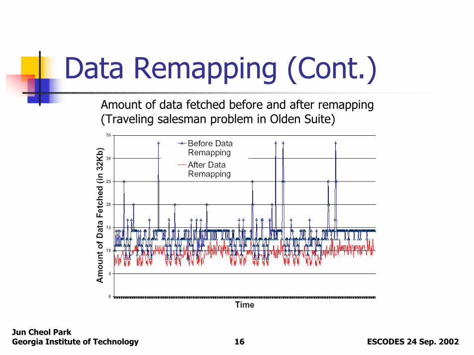
Data Remapping (Cont.)Amount of data fetched before and after remapping(Traveling salesman problem in Olden Suite)
ESCODES 24 Sep. 2002Jun Cheol ParkGeorgia Institute of Technology 17
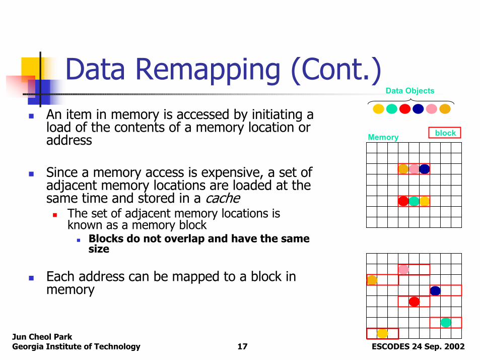
Data Remapping (Cont.)An item in memory is accessed by initiating a load of the contents of a memory location or address
Since a memory access is expensive, a set of adjacent memory locations are loaded at the same time and stored in a cache
The set of adjacent memory locations is known as a memory block
Blocks do not overlap and have the same size
Each address can be mapped to a block in memory
Data Objects
Memory block
ESCODES 24 Sep. 2002Jun Cheol ParkGeorgia Institute of Technology 18
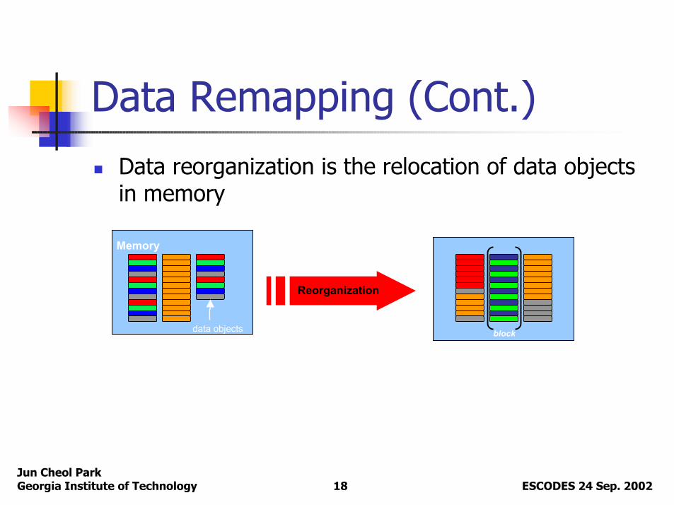
Data Remapping (Cont.)Data reorganization is the relocation of data objects in memory
block
Reorganization
data objects
Memory
ESCODES 24 Sep. 2002Jun Cheol ParkGeorgia Institute of Technology 19
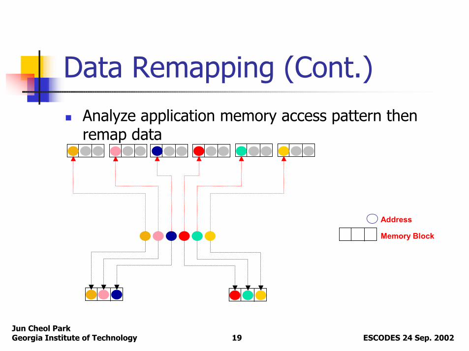
Data Remapping (Cont.)Analyze application memory access pattern thenremap data
Address
Memory Block
ESCODES 24 Sep. 2002Jun Cheol ParkGeorgia Institute of Technology 20
Voltage/frequency scaling of off-chip memory and bus*
Scaling down supply voltage of off-chip bus and memory (L2 cache)
P is proportional to V2
Significant energy saving in L2 cacheDoubling the memory access latencyL2 cache miss rate affects system performance significantly
*K. Puttaswamy, K. Choi, J. C. Park, V. J. Mooney III, A. Chatterjee and P. Ellervee, System Level Power-Performance Trade-Offs in Embedded Systems Using Voltage and Frequency Scaling of Off-Chip Busesand Memory,” Proceedings of International Symposium on System Synthesis, to appear, October, 2002, Kyoto, Japan.
ESCODES 24 Sep. 2002Jun Cheol ParkGeorgia Institute of Technology 21
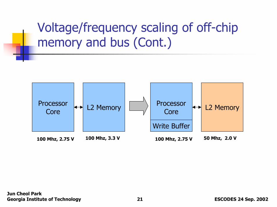
Voltage/frequency scaling of off-chip memory and bus (Cont.)
L2 MemoryProcessorCore
100 Mhz, 2.75 V 100 Mhz, 3.3 V
L2 MemoryProcessorCore
100 Mhz, 2.75 V 50 Mhz, 2.0 V
Write Buffer
ESCODES 24 Sep. 2002Jun Cheol ParkGeorgia Institute of Technology 22
Experimental ResultsTwo Olden benchmarks (Health and Perimeter) are usedThe supply voltage for L2 cache and buses are scaled down to 2V, 50MhzThe benchmarks are remapped and simulated with 50Mhz L2 cacheHalf size L1 and L2 cache system is simulated
Data remapping can achieve same execution time with half cache resources
ESCODES 24 Sep. 2002Jun Cheol ParkGeorgia Institute of Technology 23
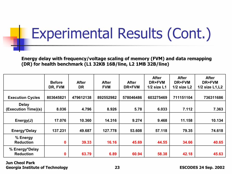
Experimental Results (Cont.)
45.6342.1858.3860.946.8963.790% Energy*Delay
Reduction
40.6534.6644.5545.6916.1639.330% EnergyReduction
74.61879.3557.11853.608127.77849.687137.231Energy*Delay
10.13411.1589.4689.27414.31610.36017.076Energy(J)
7.3637.1126.0335.788.9264.7968.036Delay
(Execution Time)(s)
736311686711151104603275469578046486892552982479612138803645821Execution Cycles
AfterDR+FVM
1/2 size L1,L2
AfterDR+FVM
1/2 size L2
AfterDR+FVM
1/2 size L1After
DR+FVMAfterFVM
AfterDR
BeforeDR, FVM
Energy delay with frequency/voltage scaling of memory (FVM) and data remapping (DR) for health benchmark (L1 32KB 16B/line, L2 1MB 32B/line)
ESCODES 24 Sep. 2002Jun Cheol ParkGeorgia Institute of Technology 24
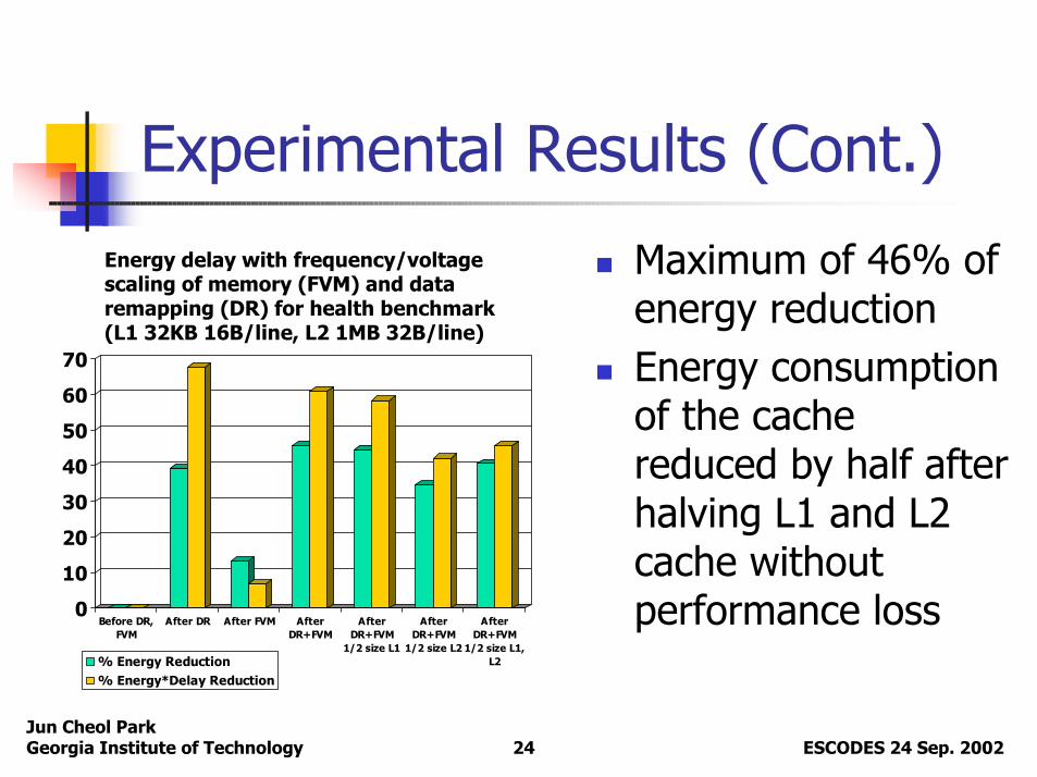
Experimental Results (Cont.)
0
10
20
30
40
50
60
70
Before DR,FVM
After DR After FVM AfterDR+FVM
AfterDR+FVM
1/2 size L1
AfterDR+FVM
1/2 size L2
AfterDR+FVM
1/2 size L1,L2% Energy Reduction
% Energy*Delay Reduction
Maximum of 46% of energy reductionEnergy consumption of the cache reduced by half after halving L1 and L2 cache without performance loss
Energy delay with frequency/voltage scaling of memory (FVM) and data remapping (DR) for health benchmark (L1 32KB 16B/line, L2 1MB 32B/line)
ESCODES 24 Sep. 2002Jun Cheol ParkGeorgia Institute of Technology 25
Conclusion
Combine of two techniques (HW & SW) to maximize energy reductionAchieve 46% of energy reduction without performance lossAchieve 1/2 energy consumption with half size cache, same performance
ESCODES 24 Sep. 2002Jun Cheol ParkGeorgia Institute of Technology 26
Thank you.