circuits and systems scaling to...
TRANSCRIPT

Circuits and Systems Scaling to Nanotechnology
December 6 – 9, 2010
Hilton Kuala Lumpur and
Le Meridien Kuala Lumpur,
Malaysia
The IEEE APCCAS 2010, the 11th biennial Asia Pacific Conference on Circuits and Systems, willbe held in Malaysia in the splendid five-star Hilton Kuala Lumpur and Le Meridien Kuala Lumpurhotels with a superb location only a stone’s throw away from the shopping and entertainmenthub surrounded by an exciting potpourri from Truly Asia, consists of Malay, Chinese, Indian,Eurasian and European. The APCCAS is a major international forum established by the IEEECircuits and Systems Society for researchers to exchange their latest findings in circuits andsystems.
Tutorials: The tutorials will be held on Monday 6th December 2010. Please submit proposals fortutorial sessions to the tutorial chair.
Special sessions: Proposals are solicited for special sessions. Please submit proposals for specialsessions to the special sessions chair.
Paper submissions: Complete 4-page manuscript (in standard IEEE double-column format),including title, authors’ names, affiliations and e-mail addresses, and a short abstract arerequested. Papers must be submitted electronically in PDF format. Only electronic submissionwill be accepted. For detailed information, please consult the conference website:http://www.apccas2010.org
The IEEE APCCAS 2010 is a meeting place for scholars, scientists, educators, students,engineers, entrepreneurs and managers. It covers a wide range of topics including, but notlimited to the following:
Conference Focus Topics
Deadline for submission of Tutorial Proposals: 20 June 2010Deadline for submission of Special Sessions Proposals: 10 June 2010Notification of acceptance of Tutorial Proposals: 30 June 2010Notification of acceptance of Special Sessions Proposal: 15 June 2010Deadline for submission of Full 4-page Papers in Regular Sessions: 30 June 2010Deadline for submission of Full 4-page Papers in Special Sessions: 10 July 2010Notification of Paper Acceptance: 15 August 2010Deadline for submission of FINAL Papers: 10 September 2010Deadline for Author and Early-Bird Registration: 10 September 2010 Conference Dates: 6-9 Dec 2010
Technical Committee
Pau-Choo ChungNational Cheng Kung University, Taiwan
Nam LingSanta Clara University, USA
Gerald SobelmanUniversity of Minnesota, USA
P Raveendran, University of Malaya, Malaysia
Randall GeigerIowa State university
Shoji KawahitoShizuoka University
Ljiljana TrajkovicSimon Fraser University
Ramesh HarjaniUniversity of Minnesota
David SkellernNational Information and Communications Technology Australia LTD
Bin-Da LiuNational Cheng Kung University
N R Narayana MurthyInfosys Technologies Limited
General ChairSudhansu Shekhar JamuarUniversity Malaya, MalaysiaEmail: [email protected]
Keynote Speakers
http://[email protected]
• Analog Signal Processing• Biomedical Engineering• Blind Signal Processing• Cellular Neural Networks and Array
Computing• Circuits and Systems for Communications• Circuits and Systems Education and Outreach• Computer-Aided Network Design• Digital Signal Processing • Life-Science Systems and Applications• Multimedia Systems and Applications
• Nanoelectronics and Gigascale Systems• Neural Systems and Applications• Nonlinear Circuits and Systems• Power Systems and Power Electronic Circuits• Sensory Systems• Visual Signal Processing and Communications• Test Technology• System-on-Chip (SOC)• Packaging• MEMS Technology
Important Dates
Hotel Venue

14.00 pm ‐ 14.20 pm 1569317431 Versatile High Input Impedance Voltage‐Mode Three‐Inputs Universal Biquadratic Filter
Jiun‐Wei Horng
14.20pm ‐ 14.40 pm 1569326681 A Tunable Transconductor With High Linearity
Vijaya Bhadauria ; Krishna Kant ; Swapna Banerjee
14.40 pm ‐ 15.00 pm 1569327805 An Unconditionally Stable Voltage Regulator
Paulo Crepaldi ; Tales C Pimenta ; Robson Moreno ; Edgar Rodriguez
15.00 pm ‐ 15.20 pm 1569328773 A New Offset Cancelled Latch Comparator for High‐Speed, Low‐Power ADCs
Khosrov Dabbagh Sadeghipour
15.20 pm ‐ 15.40 pm 1569328963 Low Power Chopper Amplifier Without LPF
Xiao Yang; Chaodong Ling
16.00 pm ‐ 16.20 pm 1569330471 Indirect Current Feedback Instrumentation Amplifier for Current Sensing
Fuding Ge
16.20pm ‐ 16.40 pm 1569334807 High‐Speed Low‐Power Single‐Stage Latched‐Comparator with Improved Gain and Kickback Noise Rejection
Sarang Kazeminia ; Morteza Mousazadeh; Khayrollah Hadidi ; Abdollah Khoei
16.40 pm ‐ 17.00 pm 1569335671 A 25MHz Sign and Magnitude Converter for Analog Current Mode Iterative Decoders
Ming Yam Lo ; Wing‐Hung Ki
17.00 pm ‐ 17.20 pm 1569335687 Current‐Mode Analog CMOS Fuzzy Logic Controller
Mohammad Soleimani ; Abdollah Khoei ; Khayrollah Hadidi
17.20 pm ‐ 17.40 pm 1569336087 A Highly Linear Open‐Loop High‐Speed CMOS Sample‐and‐Hold
Morteza Mousazadeh; Khayrollah Hadidi; Abdollah Khoei
14.00 pm ‐ 14.20 pm 1569320537 A Low‐Power Remotely‐Programmable MCU for Implantable Medical Devices
Xiaoyu Zhang ; Hanjun Jiang ; Xinkai Chen ; Chun Zhang ; Zhihua Wang ; Binjie ZHu
14.20pm ‐ 14.40 pm 1569328849 Design and Development of a Low Cost EMG Signal Acquisition System Using Surface EMG Electrode
Tarn Shi Poo ; Kenneth Sundaraj
14.40 pm ‐ 15.00 pm 1569329007 FPGA‐Based Architectures of Finite Radon Transform for Medical Image De‐Noising
Afandi Bin Ahmad ; Abbes Amira ; Hassan Rabah ; Yves Berviller
15.00 pm ‐ 15.20 pm 1569329647 A Wireless Energy Link for Endoscopy with End‐Fire Helix Emitter and Load‐Adaptive Power Converter
Tianjia Sun ; Xie Xiang ; Guolin Li; Yingke Gu ; Xiaomeng Li ; Zhihua Wang
15.20 pm ‐ 15.40 pm 1569329847 A 77 nW Bioamplifier with a Tunable Bandwidth for Neural Recording Systems
Iman Abaspur Kazerouni ; Hadi Goodarzi Dehrizi ; Sayed Mohammad Mostafavi Isfahani ; Zhuo Zou ; Majid
Baghaei‐Nejad ; Li‐Rong Zheng
16.00 pm ‐ 16.20 pm 1569329859 An Ultra‐Low Power Multi‐Tunable Triangle Wave Generator with Frequency and Amplitude Control
Sayed Mohammad Mostafavi Isfahani ; Iman Abaspur Kazerouni ; Zhuo Zou ; Majid Baghaei‐Nejad ; Li‐Rong
Zheng
16.20pm ‐ 16.40 pm 1569335837 A Power Efficient Programmable Gain Boosting Current Mirror for Biomedical Electronics
Hosung Chun
16.40 pm ‐ 17.00 pm 1569336279 Low‐Noise Amplifier Path for Ultrasound System Applications
Jayang Yoon ; Jinseok Koh ; Seok Lee ; Jaehoon Kim ; Namjin Song ; Joongho Choi
17.00 pm ‐ 17.20 pm 1569339337 CMRR Enhancement Technique for IA using Three IAs for Bio‐medical Sensor Applications
2010 IEEE Asia Pacific Conference on Circuits and Systems
Circuits and Systems Scaling to NanotechnologyDecember 6 ‐ 9, 2010 Kuala Lumpur, MALAYSIA
Sentral Ballroom B (Hilton Kuala Lumpur) Biomedical Circuits and Systems ISession Chair:
Sentral Ballroom B (Hilton Kuala Lumpur) Biomedical Circuits and Systems IISession Chair:
Oral Presentation Schedule
DAY 2: Tuesday, 7th December 2010Sentral Ballroom A ( Hilton Kuala Lumpur) Analog Sinal Processing I
Session Chair:
Sentral Ballroom A (Hilton Kuala Lumpur) Analog Sinal Processing IISession Chair:

Woojae Lee
17.20 pm ‐ 17.40 pm 1569320521 Characterization of Endothelial Cells Using Electrochemical Impedance Spectroscopy
Fei Liu; SM Arifuzzaman ; Anis Nordin ; David Spray ; Ioana Voiculescu
14.00 pm ‐ 14.20 pm 1569315333Combining Unspecified Test Data Bit Filling Methods and Run Length Based Codes to Estimate Compression,
Power and Area overhead
Usha Sandeep Mehta ; K S Dasgupta ; Niranjan Devashrayee
14.20pm ‐ 14.40 pm 1569327697 ADC Linearity Test Signal Generation Algorithm
Satoshi Uemori ; Takahiro Yamaguchi ; Satoshi Ito ; Yohei Tan; Haruo Kobayashi ; Nobukazu Takai ; Kiichi Niitsu
; N. Ishikawa
14.40 pm ‐ 15.00 pm 1569327727 A Design Platform for Analog Device Size Sensitivity Analysis and Visualization
Diming Ma ; Guoyong Shi ; Alex Lee
15.00 pm ‐ 15.20 pm 1569328215 Jitter Generation and Capture using Phase‐Domain Sigma‐Delta Encoding
Sadok Aouini; Kun Chuai ; Gordon Roberts
15.20 pm ‐ 15.40 pm 1569328623 Built‐in Self‐Test/Repair Scheme for TSV‐Based Three‐Dimensional Integrated Circuits
Hung‐Yen Huang ; Yu‐Sheng Huang ; Chun Lung Hsu
16.00 pm ‐ 16.15 pm 1569328889 Testing Techniques for Resistive‐Open Defects in Future CMOS Technologies
Mohammad Fawaz ; Nader Kobrosli ; Ali Chehab ; Ayman Kayssi
16.15pm ‐ 16.30 pm 1569329403 Transistor Sizing Analysis Approach for Sub‐Threshold Silicon‐on‐Insulator (SOI) Circuits
Ahui Sun ; Kok Leong Chang ; Kwen Siong Chong ; Bah Hwee Gwee ; Joseph Chang
16.30 pm ‐ 16.45 pm 1569329621 RedSOCs‐3D: Thermal‐safe Test Scheduling for 3D‐Stacked SoC
Fawnizu Azmadi Hussin ; Thomas Edison C Yu ; Tomokazu Yoneda ; Hideo Fujiwara
16.45 pm ‐ 17.00 pm 1569335663A 9T Subthreshold SRAM Bitcell with Data‐independent Bitline Leakage for Improved Bitline Swing and
Variation Tolerance
Qi Li ; Tony Tae Hyoung Kim
17.00 pm ‐ 17.15 pm 1569336307 Non‐Preemptive Test Scheduling for Network‐on‐Chip(NoC) Based Systems by Reusing NoC as TAM
Goutam Mali; Suman Das ; Hafizur Rahaman ; Chandan Giri
17.15 pm ‐ 17.30 pm 1569336837 Error Tolerance Methodology for Quantization in JPEG 2000 Encoder
Yu‐Sheng Huang ; Hung‐Yen Huang ; Chun Lung Hsu
14.00 pm ‐ 14.20 pm 1569319283 A 4.8‐Gb/s Mixed‐mode CMOS QPSK Demodulator For 60‐GHz Wireless Personal Area Networks
Duho Kim ; Minsu Ko ; Kwang‐chun Choi ; Woo‐young Choi
14.20pm ‐ 14.40 pm 1569335665 Design of High Linearity Low Flicker Noise 5.2 GHz Down‐Conversion Mixer for Direct Conversion Receiver
Ramesh K Pokharel ; Haruichi Kanaya ; Youichi Yano ; Mahmoud Ahmed Abdelghany ; Keiji Yoshida
14.40 pm ‐ 15.00 pm 1569336868 A Low Flicker Noise, Highly Linear, Direct Conversion Receiver for 5GHz Wireless LAN
Mahmoud Ahmed Abdelghany ; Haruichi Kanaya ; Ramesh K Pokharel ; Keiji Yoshida
15.00 pm ‐ 15.20 pm 1569340791 An Electrically Small Meander Line Antenna for Wireless Applications
Atif Jamil Shaikh
15.20 pm ‐ 15.40 pm 1569320531 A 47‐dB Linear CMOS Variable Gain Amplifier using Current Squaring Technique
Xin Cheng ; Hai‐gang Yang
16.00 pm ‐ 16.20 pm 1569325361 A 120dB All CMOS Variable Gain Amplifier Based on New Exponential Equation
Farhad Sheikhhosseini ; Abdolreza Nabavi
16.20pm ‐ 16.40 pm 1569327845 A Switch Controlled Resistor Based CMOS Programmable Gain Amplifier with DC Offset Cancellation for WSN
Xiangning Fan ; Da Cheng ; Yangyang Feng
16.40 pm ‐ 17.00 pm 1569334083 Design of Wide Band PVGA for UWB Applications
Ibrahim Lotfy Abdel‐hafez ; Yaser Khalaf ; Fathi Farag
17.00 pm ‐ 17.20 pm 1569336176 A DC‐Offset Cancellation Circuit for PGA in Baseband Communication
Guanzhong Huang ; Yingjie Wu ; Chaoli Zhong ; Pingfen Lin
Accord Network Room (Hilton Kuala Lumpur) Test Technology ISession Chair:
Accord Network Room (Hilton Kuala Lumpur) Test Technology IISession Chair:
Exchange A & B (Hilton Kuala Lumpur) Circuits and Systems for Communications ISession Chair:
Exchange A & B (Hilton Kuala Lumpur) Circuits and Systems for Communications IISession Chair:
2010 Asia Pacific Conference on Circuits and Systems (APCCAS 2010) 6 – 9 December 2010, Kuala Lumpur, Malaysia
A 4.8-Gb/s Mixed-mode CMOS QPSK Demodulator For 60-GHz Wireless Personal Area Networks
Duho Kim, Minsu Ko, Kwang-Chun Choi, and Woo-Young Choi
Department of Electrical and Electronic Engineering, Yonsei University 134, Shinchon-Dong, Sudaemoon-Ku, Seoul, Korea.
Abstract— A mixed-mode QPSK demodulator for 60-GHz wireless personal area network application is demonstrated. The prototype chip realized by 60-nm CMOS process can demodulate up to 4.8-Gb/s QPSK signals at 4.8-GHz carrier frequency. At this carrier frequency, the demodulator core consumes 54 mW from 1.2-V power supply while the chip area is 150 × 150 μm2. Using the fabricated chip, transmission and demodulation of 1.7-GSymbol/s QPSK signal in 60-GHz link is demonstrated.
Keywords— QPSK, demodulator, 60-GHz, WPAN, CMOS, mixed-mode
I. INTRODUCTION
There are growing interests for 60-GHz wireless personal area networks and the IEEE 802.15.3c standard has been recently released [1]. As the standard supports Gb/s of transmission, realization of efficient wideband demodulators becomes an important task. Although digital demodulators are widely used, the increase in the data rate makes the realizing of required ADCs challenging. The IEEE 802.15.3c specifies the sample rate of 1.7-GSymbol/s [1], and ADCs meeting this requirement consume much power and chip area. We have previously demonstrated the mixed-mode binary-phase-shift keying (BPSK) demodulation scheme using effectively 1-bit sampler, which can save power and chip area significantly [2, 3]. We showed that slicing BPSK signals with a hard limiter produces signals that are essentially NRZ data and, consequently, a mixed-mode clock and data recovery (CDR) structure can be successfully applied for demodulation of BPSK signals [3]. As an extension, we demonstrate a mixed-mode QPSK demodulator in this paper. Although 1-bit resolution sampling is not enough for complex digital processing such as frequency domain equalization to avoid degradation from multi-path fading, it relieves the linearity requirement of RF circuits and offers simple structures, which can be advantageous for short-range line-of-sight applications.
II. DEMODULATOR SCHEME
Assuming ω represents the carrier frequency and input data for each I or Q (DI, DQ) have 1 for ‘high (H)’ and -1 for ‘low (L)’, the QPSK-modulated signal (MOD) can be represented as
MOD = DI cos ωt + DQ sin ωt.
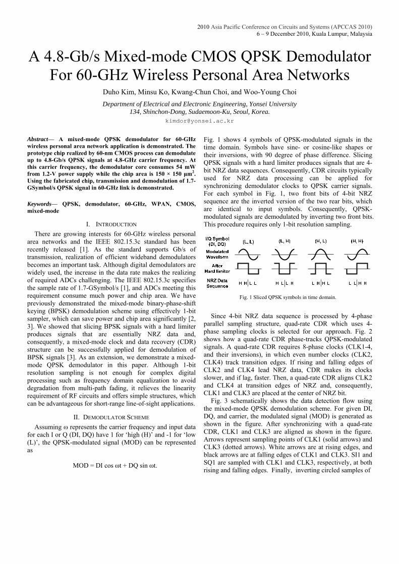
Fig. 1 shows 4 symbols of QPSK-modulated signals in the time domain. Symbols have sine- or cosine-like shapes or their inversions, with 90 degree of phase difference. Slicing QPSK signals with a hard limiter produces signals that are 4-bit NRZ data sequences. Consequently, CDR circuits typically used for NRZ data processing can be applied for synchronizing demodulator clocks to QPSK carrier signals. For each symbol in Fig. 1, two front bits of 4-bit NRZ sequence are the inverted version of the two rear bits, which are identical to input symbols. Consequently, QPSK-modulated signals are demodulated by inverting two front bits. This procedure requires only 1-bit resolution sampling.
Fig. 1 Sliced QPSK symbols in time domain.
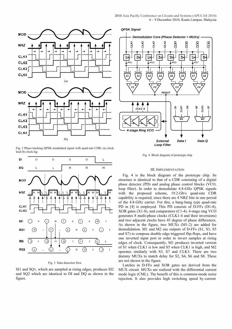
Since 4-bit NRZ data sequence is processed by 4-phase
parallel sampling structure, quad-rate CDR which uses 4-phase sampling clocks is selected for our approach. Fig. 2 shows how a quad-rate CDR phase-tracks QPSK-modulated signals. A quad-rate CDR requires 8-phase clocks (CLK1-4, and their inversions), in which even number clocks (CLK2, CLK4) track transition edges. If rising and falling edges of CLK2 and CLK4 lead NRZ data, CDR makes its clocks slower, and if lag, faster. Then, a quad-rate CDR aligns CLK2 and CLK4 at transition edges of NRZ and, consequently, CLK1 and CLK3 are placed at the center of NRZ bit.
Fig. 3 schematically shows the data detection flow using the mixed-mode QPSK demodulation scheme. For given DI, DQ, and carrier, the modulated signal (MOD) is generated as shown in the figure. After synchronizing with a quad-rate CDR, CLK1 and CLK3 are aligned as shown in the figure. Arrows represent sampling points of CLK1 (solid arrows) and CLK3 (dotted arrows). White arrows are at rising edges, and black arrows are at falling edges of CLK1 and CLK3. SI1 and SQ1 are sampled with CLK1 and CLK3, respectively, at both rising and falling edges. Finally, inverting circled samples of
2010 Asia Pacific Conference on Circuits and Systems (APCCAS 2010) 6 – 9 December 2010, Kuala Lumpur, Malaysia
Fig. 2 Phase-tracking QPSK-modulated signal with quad-rate CDR; (a) clock lead (b) clock lag
Fig. 3 Data detection flow
SI1 and SQ1, which are sampled at rising edges, produces SI2 and SQ2 which are identical to DI and DQ as shown in the figure.
4-stage Ring VCO
Demodulator Core (Phase Detector + MUXs)
CLK1~4
PDOUT
QPSK Signal
S1 S3 S5 S7
M2M1
C1 C2 C3 C4
X1 X3 X5 X7X2 X4 X6 X8
ExternalLoop Filter
Data I Data Q
Fig. 4 Block diagram of prototype chip
III. IMPLEMENTATION
Fig. 4 is the block diagram of the prototype chip. Its structure is identical to that of a CDR consisting of a digital phase detector (PD) and analog phase control blocks (VCO, loop filter). In order to demodulate 4.8-GHz QPSK signals with the proposed scheme, 19.2-Gb/s quad-rate CDR capability is required, since there are 4 NRZ bits in one period of the 4.8-GHz carrier. For this, a bang-bang type quad-rate PD in [4] is employed. This PD consists of D-FFs (D1-8), XOR gates (X1-8), and comparators (C1-4). 4-stage ring VCO generates 8 multi-phase clocks (CLK1-4 and their inversions) and two adjacent clocks have 45 degree of phase differences. As shown in the figure, two MUXs (M1-2) are added for demodulation. M1 and M2 use outputs of D-FFs (S1, S3, S5 and S7) to compose double edge triggered flip-flops, and have one inverted input port in order to invert samples at rising edges of clock. Consequently, M1 produces inverted version of S1 when CLK1 is low and S5 when CLK1 is high, and M2 operates similarly with S3, S7 and CLK3. There are two dummy MUXs to match delay for S2, S4, S6 and S8. These are not shown in the figure.
Latches in D-FFs and XOR gates are derived from the MUX circuit. MUXs are realized with the differential current mode logic (CML). The benefit of this is common-mode noise rejection. It also provides high switching speed by current
2010 Asia Pacific Conference on Circuits and Systems (APCCAS 2010) 6 – 9 December 2010, Kuala Lumpur, Malaysia
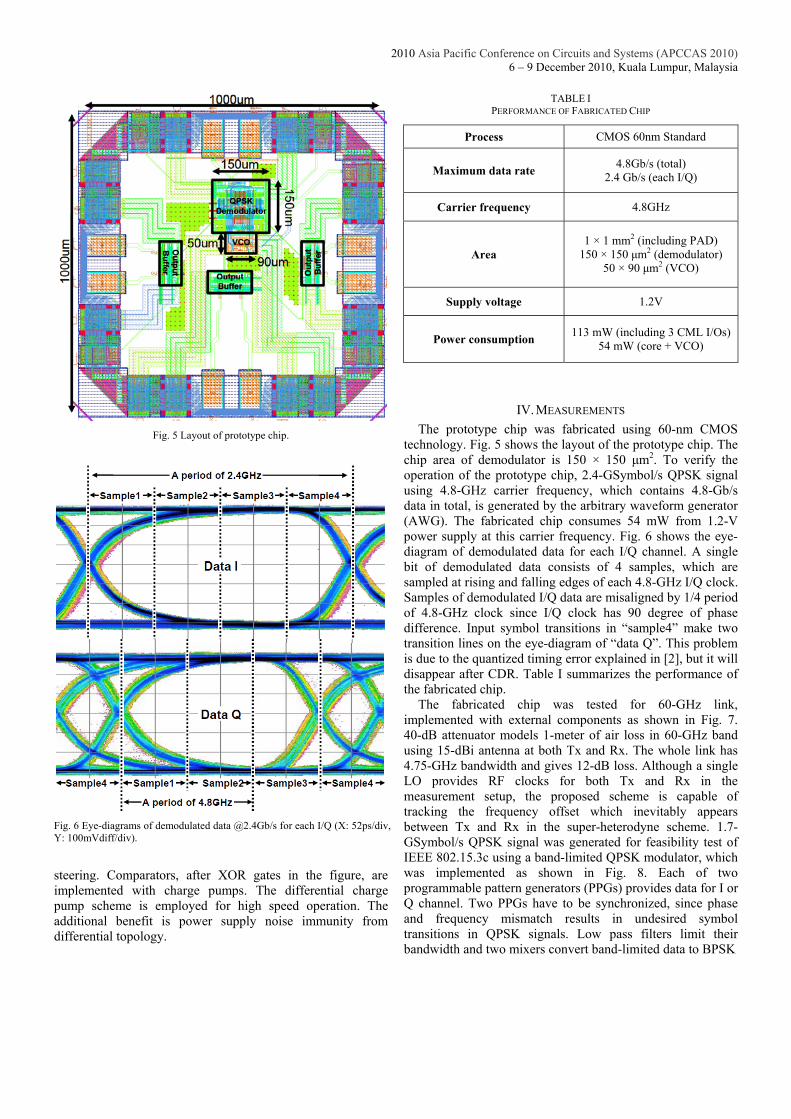
Fig. 5 Layout of prototype chip.
Fig. 6 Eye-diagrams of demodulated data @2.4Gb/s for each I/Q (X: 52ps/div, Y: 100mVdiff/div).
steering. Comparators, after XOR gates in the figure, are implemented with charge pumps. The differential charge pump scheme is employed for high speed operation. The additional benefit is power supply noise immunity from differential topology.
TABLE I PERFORMANCE OF FABRICATED CHIP
Process CMOS 60nm Standard
Maximum data rate 4.8Gb/s (total)
2.4 Gb/s (each I/Q)
Carrier frequency 4.8GHz
Area 1 × 1 mm2 (including PAD)
150 × 150 μm2 (demodulator) 50 × 90 μm2 (VCO)
Supply voltage 1.2V
Power consumption 113 mW (including 3 CML I/Os)
54 mW (core + VCO)
IV. MEASUREMENTS
The prototype chip was fabricated using 60-nm CMOS technology. Fig. 5 shows the layout of the prototype chip. The chip area of demodulator is 150 × 150 μm2. To verify the operation of the prototype chip, 2.4-GSymbol/s QPSK signal using 4.8-GHz carrier frequency, which contains 4.8-Gb/s data in total, is generated by the arbitrary waveform generator (AWG). The fabricated chip consumes 54 mW from 1.2-V power supply at this carrier frequency. Fig. 6 shows the eye-diagram of demodulated data for each I/Q channel. A single bit of demodulated data consists of 4 samples, which are sampled at rising and falling edges of each 4.8-GHz I/Q clock. Samples of demodulated I/Q data are misaligned by 1/4 period of 4.8-GHz clock since I/Q clock has 90 degree of phase difference. Input symbol transitions in “sample4” make two transition lines on the eye-diagram of “data Q”. This problem is due to the quantized timing error explained in [2], but it will disappear after CDR. Table I summarizes the performance of the fabricated chip.
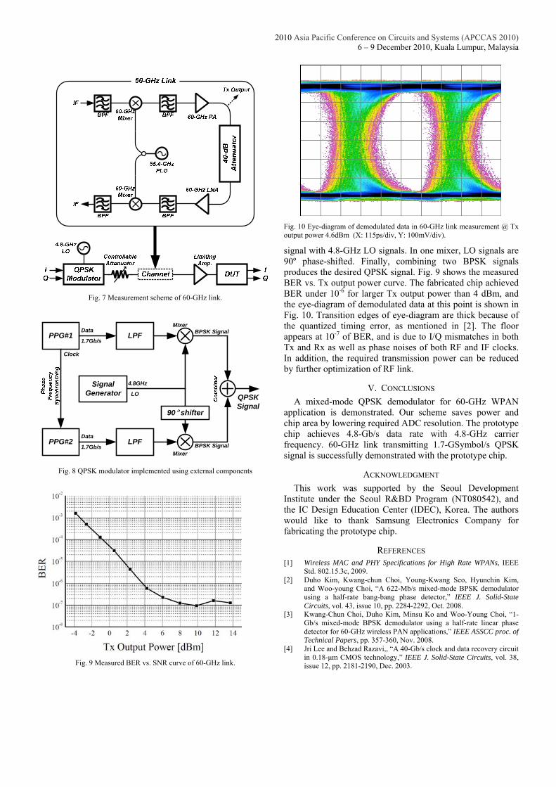
The fabricated chip was tested for 60-GHz link, implemented with external components as shown in Fig. 7. 40-dB attenuator models 1-meter of air loss in 60-GHz band using 15-dBi antenna at both Tx and Rx. The whole link has 4.75-GHz bandwidth and gives 12-dB loss. Although a single LO provides RF clocks for both Tx and Rx in the measurement setup, the proposed scheme is capable of tracking the frequency offset which inevitably appears between Tx and Rx in the super-heterodyne scheme. 1.7-GSymbol/s QPSK signal was generated for feasibility test of IEEE 802.15.3c using a band-limited QPSK modulator, which was implemented as shown in Fig. 8. Each of two programmable pattern generators (PPGs) provides data for I or Q channel. Two PPGs have to be synchronized, since phase and frequency mismatch results in undesired symbol transitions in QPSK signals. Low pass filters limit their bandwidth and two mixers convert band-limited data to BPSK
2010 Asia Pacific Conference on Circuits and Systems (APCCAS 2010) 6 – 9 December 2010, Kuala Lumpur, Malaysia
Fig. 7 Measurement scheme of 60-GHz link.
PPG#1
PPG#2
SignalGenerator
LPF
LPF
Data
Clock
4.8GHz
LO
1.7Gb/s
Data
1.7Gb/s
90 shifter
Mixer
Mixer
QPSKSignal
BPSK Signal
BPSK Signal
Fig. 8 QPSK modulator implemented using external components
Fig. 9 Measured BER vs. SNR curve of 60-GHz link.
Fig. 10 Eye-diagram of demodulated data in 60-GHz link measurement @ Tx output power 4.6dBm (X: 115ps/div, Y: 100mV/div).
signal with 4.8-GHz LO signals. In one mixer, LO signals are 90º phase-shifted. Finally, combining two BPSK signals produces the desired QPSK signal. Fig. 9 shows the measured BER vs. Tx output power curve. The fabricated chip achieved BER under 10-6 for larger Tx output power than 4 dBm, and the eye-diagram of demodulated data at this point is shown in Fig. 10. Transition edges of eye-diagram are thick because of the quantized timing error, as mentioned in [2]. The floor appears at 10-7 of BER, and is due to I/Q mismatches in both Tx and Rx as well as phase noises of both RF and IF clocks. In addition, the required transmission power can be reduced by further optimization of RF link.
V. CONCLUSIONS
A mixed-mode QPSK demodulator for 60-GHz WPAN application is demonstrated. Our scheme saves power and chip area by lowering required ADC resolution. The prototype chip achieves 4.8-Gb/s data rate with 4.8-GHz carrier frequency. 60-GHz link transmitting 1.7-GSymbol/s QPSK signal is successfully demonstrated with the prototype chip.
ACKNOWLEDGMENT
This work was supported by the Seoul Development Institute under the Seoul R&BD Program (NT080542), and the IC Design Education Center (IDEC), Korea. The authors would like to thank Samsung Electronics Company for fabricating the prototype chip.
REFERENCES [1] Wireless MAC and PHY Specifications for High Rate WPANs, IEEE
Std. 802.15.3c, 2009. [2] Duho Kim, Kwang-chun Choi, Young-Kwang Seo, Hyunchin Kim,
and Woo-young Choi, “A 622-Mb/s mixed-mode BPSK demodulator using a half-rate bang-bang phase detector,” IEEE J. Solid-State Circuits, vol. 43, issue 10, pp. 2284-2292, Oct. 2008.
[3] Kwang-Chun Choi, Duho Kim, Minsu Ko and Woo-Young Choi, “1-Gb/s mixed-mode BPSK demodulator using a half-rate linear phase detector for 60-GHz wireless PAN applications,” IEEE ASSCC proc. of Technical Papers, pp. 357-360, Nov. 2008.
[4] Jri Lee and Behzad Razavi,, “A 40-Gb/s clock and data recovery circuit in 0.18-μm CMOS technology,” IEEE J. Solid-State Circuits, vol. 38, issue 12, pp. 2181-2190, Dec. 2003.