charge conduction process and rectification effect...
TRANSCRIPT
Indian Journal of Engineering & Materials Sciences Vol. 7, October-December 2000, pp. 282-286
Charge conduction process and rectification effect in ITO/doped PPy/Ag device
M S Rol, Pratibha laiswal', Manmeeta', Dhiraj Saxenab & G D Sharmab
a Defence Laboratory, Jodhpur 34200 I, India b Department of Physics, J N V University, Jodhpur 342001, India
Received 25 February 2000; accepted 14 November 2000
Electrical, impedance and photovoltaic measurements with a thin film of PMB doped PPy and undoped PPy , using sandwich between Ag and ITO are explained in terms of p-type semiconducting behaviour of PMB doped-PPy (PMB:PPy) film and by the formation of Schottky barrier with Ag and ohmic contact with ITO. At low voltage region Ohm's law is followed, while at high voltage region a space charge limited conduction is observed which is controlled by the exponential trap distribution.
The organic molecular and polymeric materials are emerging as a class of novel materials because of their potential applications in electronic and opto-electronic devices such as photovoltaic device, light emitting diodes and photorefractive devices, as these materials possess the special electrical and optical properties, low cost of processing and moreover their properties can modified by simple doping process l
•2
•
Photoinduced electron transfer process has been intensively studied in order to study the key steps in efficient conversion process. A great deal of theoretical and experimental work has shown that controlling the electron transfer rates requires control of both electronic and structural properties of the system3.4.
In the present communication, a charge transfer complex is generated by employing the spatial arrangement of molecular donor and acceptor, which under illumination leads to the creation of photo carriers at the interface existing between molecular materials. The poly-pyrrole (PPy ), a well-known ptype organic semiconducting material , was doped with a a' phenyl methyl substituted bipyridyl halide (PMB) which acts as an electron acceptor. The film of the material was developed by employing spin coating technique onto indium tin oxide (ITO) coated glass substrate. Silver (Ag) was used as a contact electrode, on the top of organic material. The active area of the device was about 1 cm2
• The J- V characteristics in dark as well as under illumination have been recorded. The J- V characteristics in dark shows the rectification effect, when the ITO electrode is made the positive with respect to Ag electrode. The rectification effect is due to the blocking contact
which is formed between PMB doped PPy and Ag. The rectification effect improves on PMB doping. The position of Fermi level shift toward the valence band which results in the increase in the free carriers concentration, Le., holes in the organic material, i.e., in PMB:PPy complex. The increase in dark conductivity on doping is due to the increase in the hole mobility. The various electrical parameters such as ideality factor, fill factor, barrier height, carrier mobility and conversion efficiency of the material have been evaluated and discussed.
Experimental Procedure The thin films of PMB doped PPy having thickness
of about 600 nm were made by spin coating technique using di-methyl formamide (DMF) as solvent on the indium tin oxide (ITO) coated glass substrate. The metallic Ag electrode was developed with silver paint on the top of the organic film for contact purpose. The J- V characteristics of the device were measured with a Keithley electrometer model 610C and a stabilised power supply. The ITO electrode was held at positive potential relative to Ag electrode. The impedance measurements were made with Keithley LCZ (Model 3330) impedance analyser. Temperature dependence of the current - voltage characteristics and impedance were measured in the range 300 - 370 K by controlling the temperature with the help of a digital temperature controller.
Results and Discussion Current· Voltage characteristics
The current-voltage characteristics of ITOI PMB:PPy/Ag device were recorded at room
ROY et af.: ITO/DOPED PPy/Ag DEVICE 283
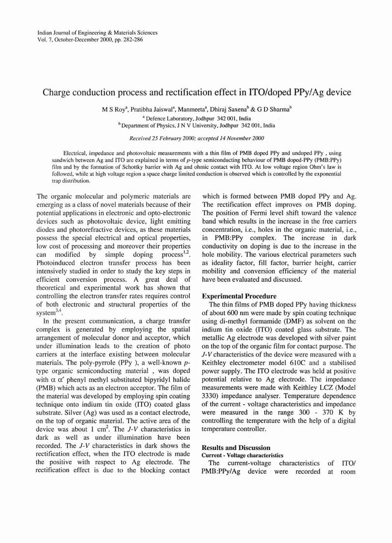
temperature and shown in Fig. 1. The forward bias corresponds to the positive potential to the ITO electrode with respect to Ag. These characteristics shows the rectification effect. The forward bias corresponds to the positive potential to the ITO electrode with respect to Ag. These characteristics indicates the formation of the Schottky barrier at Ag -PMB:PPy interface in the device while the ITO forms the ohmic contact with PMB:PPy. This behaviour can be explained by the low work function of Ag and ptype semiconductivity of PMB:PPy layer. Above the voltage forward bias the current becomes almost linear which suggest that the current is limited by the series resistance of the bulk conductive region.
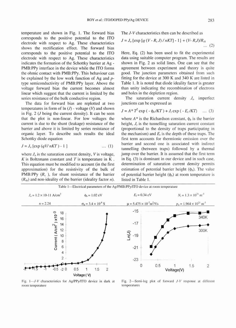
The data for forward bias are replotted at two temperatures in form of In (1) - voltage (V) and shown in Fig. 2 (J bei ng the current density). It can be seen that the plot is non-linear. For low voltages the current is due to the shunt (leakage) resistance of the barrier and above it is limited by series resistance of organic layer. To describe such results the ideal Schottky diode equation
1=1o [exp(qVlnKT)-I] ... (I)
where 10 is the saturation current density, V is voltage, K is Boltzmann constant and T is temperature in K . This equation must be modified to account (in the first approximation) for the resistivity of the bulk of PMB:PPy (Rs ), for shunt resistance of the barrier (Rsh) and non-ideality of the barrier (ideality factor n).
The 1- V characteristics then can be described as
1 = 10 {exp [q (V - R" 1) I nKT] - I} + (V- RJ)/R.,iI (2)
Here, Eq. (2) has been used to fit the experimental data using suitable computer program. The results are shown in Fig. 2 as solid lines. One can see that the agreement between experiment and theory is quite good. The junction parameters obtained from such fitting for the device at 300 K and 340 K are li sted in Table I. It is noted that diode ideality factor is greater than unity indicating the recombination of electrons and holes in the depletion region.
The saturation current density 10 imperfect junctions can be expressed as
1 = A * r exp ( - ct>b IKT) + 1( exp ( - £( IK7) ... (3)
where A * is the Richardson constant, ct>b is the barrier height, 1( is the tunnelling saturat ion current constant (proportional to the densi ty of traps participating in the mechanism) and £( is the depth of these traps. The first term accounts for thermionic emission over the barrier and second one is associated with indirect tunnelling (between traps) followed by a thermal jump over the barrier. It is assumed that the first term in Eq. (3) is dominant in our device and in such case, determination of saturation current density permits estimation of potential barrier height (ct>b)' The value of potenti al barrier height (ct>b) at room temperature is listed in Table I.
Table I-Electrical parameters of the Ag/PMB :PPyIITO device at room temperature
Jo = 1.2 x 10- 11 Alcm2 <Pt, = 1.02eV
1/ = 2.24 ad = 3.4 x 10⁻⁸ S
O'l 18 T
<=> ..-16 + x
NE 14 + <.) 12 1 ~
,
lO t .... c: 8 1 <II .... ....
6 1 :::l ()
,
4 ~
2 I-- I - 1-_.
-1 -0.5 -20 0.5 1
Voltage (V)
Fig. I-J-V characterist ics for Ag/PPy/lTO dev ice in dark at room temperature
Er= 0.34 eV
-15
340K
-17
300K -, C -19 -I
-21
-23
o 0.5 1 1.5 2 Voltage(V)
Fig. 2-Semi-Iog plot of forward J- V response at different temperatures
284 INDIAN J ENG. MATER. SCI., OCTOBER-DECEMBER 2000
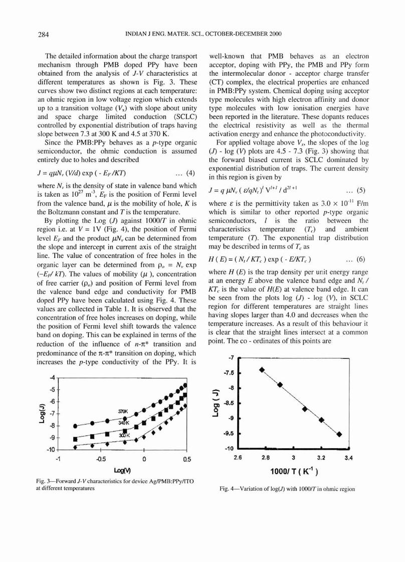
The detailed information about the charge transport mechanism through PMB doped PPy have been obtained from the analysis of J- V characteristics at different temperatures as shown is Fig. 3. These curves show two distinct regions at each temperature: an ohmic region in low voltage region which extends up to a transition voltage (Vx) with slope about unity and space charge limited conduction (SCLC) controlled by exponential distribution of traps having slope between 7.3 at 300 K and 4.5 at 370 K.
Since the PMB:PPy behaves as a p-type organic semiconductor, the ohmic conduction is assumed entirely due to holes and described
J = qJ1Nv (Vld) exp ( - EF IKn ... (4)
where Nv is the density of state in valence band which is taken as 1027 m-3, EF is the position of Fermi level from the valence band, J-l is the mobility of hole, K is the Boltzmann constant and T is the temperature.
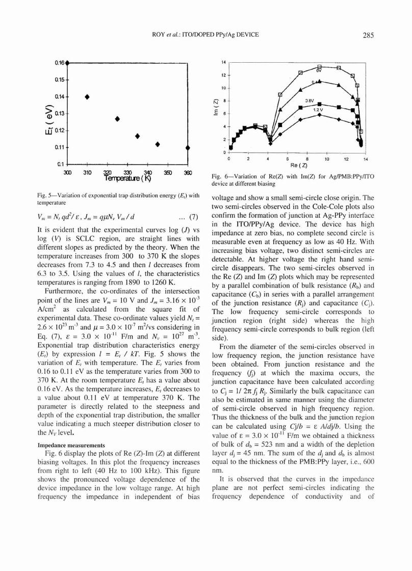
By plotting the Log (1) against 1000lT in ohmic region i.e. at V = 1 Y (Fig. 4), the position of Fermi level EF and the product J1Nv can be determined from the slope and intercept in current axis of the straight line. The value of concentration of free holes in the organic layer can be determined from Po = Nv exp (-E~ kD. The values of mobility (J-l ), concentration of free carrier (Po) and position of Fermi level from the valence band edge and conductivity for PMB doped PPy have been calculated using Fig. 4 . These values are collected in Table 1. It is observed that the concentration of free holes increases on doping, while the position of Fermi level shift towards the valence band on doping. This can be explained in terms of the reduction of the influence of n-n* transition and predominance of the n-n* transition on doping, which Increases the p-type conductivity of the PPy. It is
-4
..s -0
S-- -7 t» 0
...J -8
-9
-10
-1 ~.5 0 0.5
Fig. 3-Forward J-V characteristics for device AgIPMB:PPyIITO at different temperatures
well-known that PMB behaves as an electron acceptor, doping with PPy, the PMB and PPy form the intermolecular donor - acceptor charge transfer (CT) complex, the electrical properties are enhanced in PMB:PPy system. Chemical doping using acceptor type molecules with high electron affinity and donor type molecules with low ionisation energies have been reported in the literature. These dopants reduces the electrical resistivity as well as the thermal activation energy and enhance the photoconductivity .
For applied voltage above VI"' the slopes of the log (1) - log (V) plots are 4 .5 - 7.3 (Fig. 3) showing that the forward biased current is SCLC dominated by exponential distribution of traps. The current density in this region is given by
J = q J1Nv ( E/qNt )' y/+1 I d21 +1 (5)
where E is the permittivity taken as 3.0 x 10.11 F/m which is similar to other reported p-type organic semiconductors, l is the ratio between the characteristics temperature (TJ and ambient temperature (n. The exponential trap distributi on may be described in terms of Tc as
H ( E) = ( Nt I KTc) exp ( - EIKTc ) .. . (6)
where H (E) is the trap density per unit energy range at an energy E above the valence band edge and Nt I KTc is the value of H(E) at valence band edge. It can be seen from the plots log (1) - log (V), in SCLC region for different temperatures are straight lines having slopes larger than 4.0 and decreases when the temperature increases. As a result of this behaviour it is clear that the straight lines intersect at a common point. The co - ordinates of this points are
-7 p-------------------------~
-7.5
- ..s ""'). -O) -8.5 0
-oJ -9
·9.5
-10
2.6 2.8 3 3.2 3.4
10001 T ( K-1 )
Fig. 4-Variation of log(J) with lOOOIT in ohmic region
ROY et at. : ITO/DOPED PPy/Ag DEVICE 285
0.16
0.15
0.14 • --~ 0.13 • --ill 0.12 • 0.11 • o.1 ~--~--~----~---+----r---~
:m 310 3al :m 340 Tell p;ratt.re ( K)
Fig. 5-Variation of exponential trap distribution energy (£,) with temperature
... (7)
It is evident that the experimental curves log (1) vs log (V) is SCLC region, are straight li nes with different slopes as predicted by the theory. When the temperature increases from 300 to 370 K the slopes decreases from 7.3 to 4 .5 and then 1 decreases from 6.3 to 3.5. Using the values of I, the characteristics temperatures is ranging from 1890 to 1260 K.
Furthermore, the co-ordinates of the intersection point of the lines are VIII = 10 V and Jill = 3.16 X 10⁻³
A/cm2 as calculated from the square fit of experimental data . These co-ordinate values yield Nr = 2.6 X 10²³ m-3 and J1 = 3.0 X 10⁻⁷ m2/vs considering in Eq. (7), E = 3.0 X 10⁻¹¹ F/m and N" = 1027 m-3.
Exponential trap distribution characteristics energy (Er) by express ion 1 = Er / kT. Fig. 5 shows the variation of Er with temperature. The Er varies from 0.16 to 0.11 e V as the temperature varies from 300 to 370 K. At the room temperature Er has a value about 0. 16 e V. As the temperature increases, Er decreases to a value about 0.11 eV at temperature 370 K. The parameter is directly related to the steepness and depth of the exponential trap distribution, the smaller value indicating a much steeper distribution closer to the Nv level.
Impedance measurements Fig. 6 display the plots of Re (2)-Im (2) at different
biasing voltages. In this plot the freq uency increases from right to left (40 Hz to 100 kHz). This figure shows the pronounced voltage dependence of the device impedance in the low voltage range. At high frequency the impedance in independent of bias
H -----------------------------------
12
10
N 8
E 6
4
0+----+----+----+----+----+--- ----__ o 2 6 8 10 12 14
Re ( Z)
Fig. 6-Variation of Re(Z) with Im(Z) for AgIPMB :PPyIITO device at different biasing
voltage and show a small semi-circle close origi n. The two semi-ci rcles observed in the Cole-Cole plots also confirm the formation of j unction at Ag-PPy interface in the ITO/PPy/Ag device. The device has high impedance at zero bias, no complete second circle is measurable even at freq uency as low as 40 Hz. With increasing bias voltage, two distinct semi-circles are detectable. At higher voltage the right hand semicircle disappears. The two semi-circles observed in the Re (2) and 1m (2) plots which may be represented by a parallel combi nation of bulk resistance (Rb) and capacitance (Cb) in series with a parallel arrangement of the junction resistance (Rj ) and capacitance (Cj ) .
The low freq uency semi-circle corresponds to junction region (right side) whereas the hi gh frequency semi-circle corresponds to bulk region (left side).
From the diameter of the semi-circles observed in low frequency region, the junction resistance have been obtained. From junction resistance and the frequency (fj) at which the maxima occurs, the junction capacitance have been calculated according
to Cj = 1I2n/j Rj • Similarly the bulk capacitance can also be estimated in same manner using the diameter of semi-circle observed in high frequency region. Thus the thickness of the bulk and the junction region can be calculated using Cjlb = £ A/dj/b. Usi ng the value of £ = 3.0 X 10⁻¹¹ F/m we obtained a thickness of bulk of db = 523 nm and a width of the depletion layer dj = 45 nm. The sum of the dj and db is almost equal to the thickness of the PMB:PPy layer, i.e. , 600 nm.
It is observed that the curves in the impedance plane are not perfect semi-circles indicating the frequency dependence of conductivity and of

286 INDIAN 1 ENG. MATER. SCI., OCTOBER-DECEMBER 2000
dielectric constant, as well as spatial in-homogeneities in the device thickness and dopant concentration.
References I Wasielelewski M R, Chem. Rev, 92, (1992) 435.
2 Kazuko Takahashi , Takayasu Nihira. Kimio Akiyama & Emiko Fukuyo, J Chem Soc, Chem COIllIllIl, 8 (1992) 620.
3 Ostergard T, Pal A 1 & Stubb A, J Appl .Phys , 83 (1998) 2338.
4 Sharma G D, Gupta S K & Roy M S, SYllthetic Metal, 95 (1998) 225-232.