carbon nanotubes – redefining electronics · carbon nanotubes – redefining electronics prithu...
TRANSCRIPT
Carbon nanotubes – redefining electronics Prithu Sharma, Prerit Ahuja, Arpit Jain, Ramakrishnan K and PG Sai Srinivas
“They are stronger than steel, but the most important uses for these threadlike macromolecules are in faster, more efficient and more durable electronic devices.” 1. INTRODUCTION They’re six times lighter and a hundred times stronger than steel, and could play a big part in the future of construction. Some behave like metal conductors while others act like semiconductors [1], and they might form the basis of future computers. They can also move heat through themselves better than diamonds, and might be used industrially.
They’re carbon nanotubes — perfect molecules as small as a billionth of a meter in diameter, and the darlings of the nanotechnology field. Nearly 15 years ago Sumio Iijima, sitting at an electron microscope at the NEC Fundamental Research Laboratory in Tsukuba, Japan, first noticed odd nanoscopic threads lying in a smear of soot [2]. Made of pure carbon, as regular and symmetric as crystals, these exquisitely thin, impressively long macromolecules soon became known as nanotubes, and they have been the object of intense scientific study ever since.
In the long term, perhaps the most valuable applications will take further advantage of nanotubes’ unique electronic properties. Carbon nanotubes can in principle play the same role as silicon does in electronic circuits, but at a molecular scale where silicon and other standard semiconductors cease to work. Although the electronics industry is already pushing the critical dimensions of transistors in commercial chips below 200 nanometers (billionths of a meter)—about 400 atoms wide—engineers face large obstacles in continuing this miniaturization. Within this period, the materials and processes on which the computer revolution has been built will begin to hit fundamental physical limits. Still, there are huge economic incentives to shrink devices further, because the speed, density and efficiency of microelectronic devices all rise rapidly as the minimum feature size decreases. Experiments over the past several years have given researchers hope that wires and functional devices tens of nanometers or smaller in size could be made from nanotubes and incorporated into electronic circuits that work far faster and on much less power than those existing today.
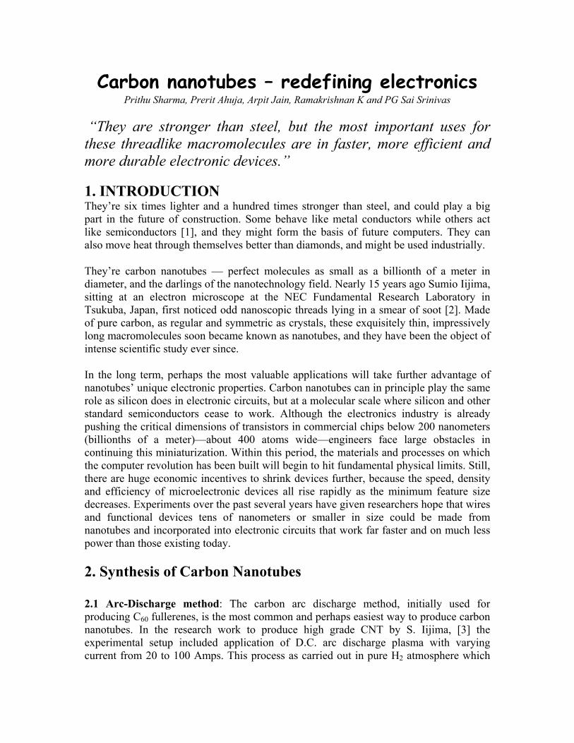
2. Synthesis of Carbon Nanotubes 2.1 Arc-Discharge method: The carbon arc discharge method, initially used for producing C60 fullerenes, is the most common and perhaps easiest way to produce carbon nanotubes. In the research work to produce high grade CNT by S. Iijima, [3] the experimental setup included application of D.C. arc discharge plasma with varying current from 20 to 100 Amps. This process as carried out in pure H2 atmosphere which
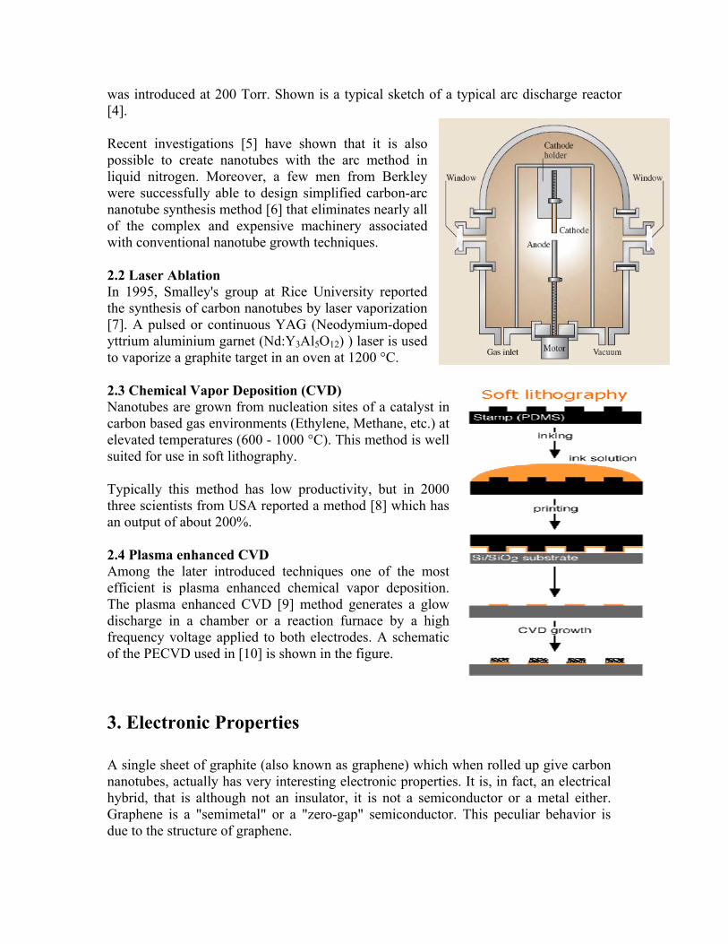
was introduced at 200 Torr. Shown is a typical sketch of a typical arc discharge reactor [4]. Recent investigations [5] have shown that it is also possible to create nanotubes with the arc method in liquid nitrogen. Moreover, a few men from Berkley were successfully able to design simplified carbon-arc nanotube synthesis method [6] that eliminates nearly all of the complex and expensive machinery associated with conventional nanotube growth techniques. 2.2 Laser Ablation In 1995, Smalley's group at Rice University reported the synthesis of carbon nanotubes by laser vaporization [7]. A pulsed or continuous YAG (Neodymium-doped yttrium aluminium garnet (Nd:Y3Al5O12) ) laser is used to vaporize a graphite target in an oven at 1200 °C. 2.3 Chemical Vapor Deposition (CVD) Nanotubes are grown from nucleation sites of a catalyst in carbon based gas environments (Ethylene, Methane, etc.) at elevated temperatures (600 - 1000 °C). This method is well suited for use in soft lithography. Typically this method has low productivity, but in 2000 three scientists from USA reported a method [8] which has an output of about 200%. 2.4 Plasma enhanced CVD Among the later introduced techniques one of the most efficient is plasma enhanced chemical vapor deposition. The plasma enhanced CVD [9] method generates a glow discharge in a chamber or a reaction furnace by a high frequency voltage applied to both electrodes. A schematic of the PECVD used in [10] is shown in the figure. 3. Electronic Properties A single sheet of graphite (also known as graphene) which when rolled up give carbon nanotubes, actually has very interesting electronic properties. It is, in fact, an electrical hybrid, that is although not an insulator, it is not a semiconductor or a metal either. Graphene is a "semimetal" or a "zero-gap" semiconductor. This peculiar behavior is due to the structure of graphene.
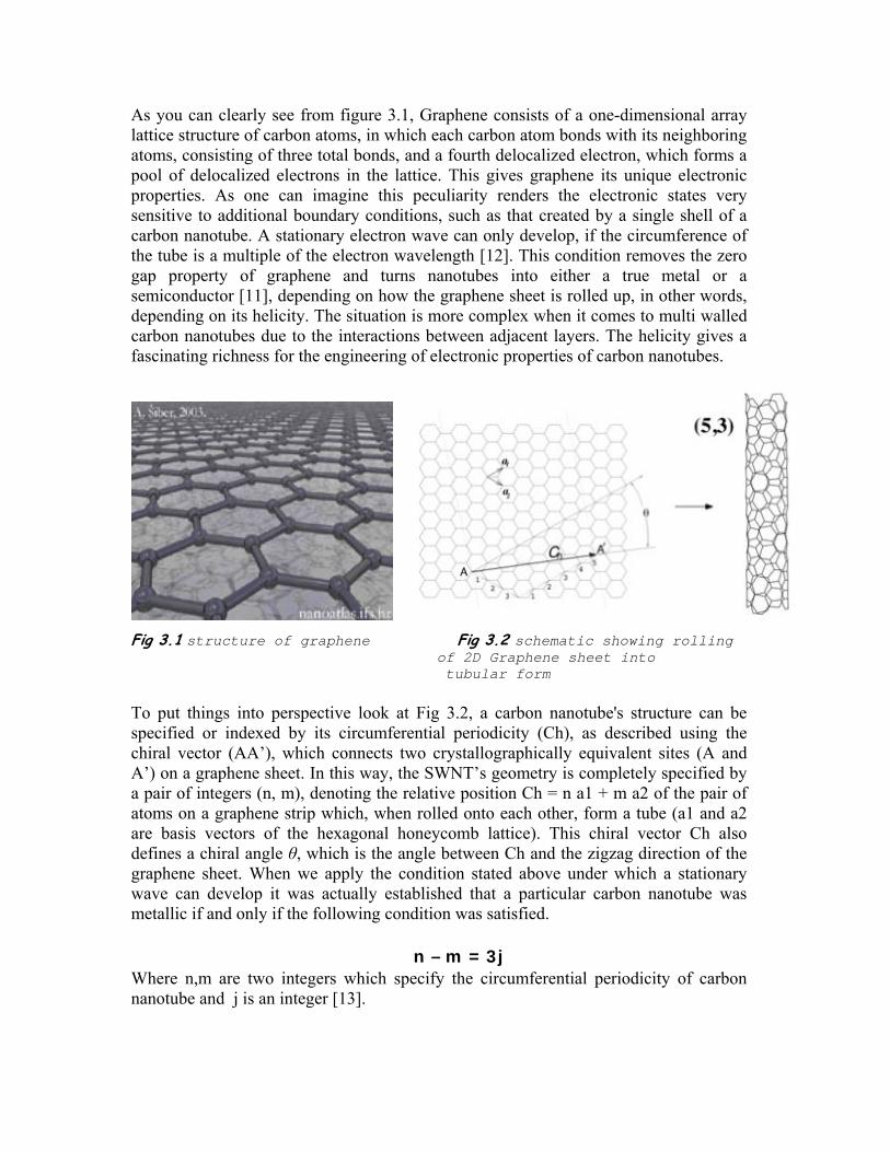
As you can clearly see from figure 3.1, Graphene consists of a one-dimensional array lattice structure of carbon atoms, in which each carbon atom bonds with its neighboring atoms, consisting of three total bonds, and a fourth delocalized electron, which forms a pool of delocalized electrons in the lattice. This gives graphene its unique electronic properties. As one can imagine this peculiarity renders the electronic states very sensitive to additional boundary conditions, such as that created by a single shell of a carbon nanotube. A stationary electron wave can only develop, if the circumference of the tube is a multiple of the electron wavelength [12]. This condition removes the zero gap property of graphene and turns nanotubes into either a true metal or a semiconductor [11], depending on how the graphene sheet is rolled up, in other words, depending on its helicity. The situation is more complex when it comes to multi walled carbon nanotubes due to the interactions between adjacent layers. The helicity gives a fascinating richness for the engineering of electronic properties of carbon nanotubes.
Fig 3.1 structure of graphene Fig 3.2 schematic showing rolling of 2D Graphene sheet into
tubular form To put things into perspective look at Fig 3.2, a carbon nanotube's structure can be specified or indexed by its circumferential periodicity (Ch), as described using the chiral vector (AA’), which connects two crystallographically equivalent sites (A and A’) on a graphene sheet. In this way, the SWNT’s geometry is completely specified by a pair of integers (n, m), denoting the relative position Ch = n a1 + m a2 of the pair of atoms on a graphene strip which, when rolled onto each other, form a tube (a1 and a2 are basis vectors of the hexagonal honeycomb lattice). This chiral vector Ch also defines a chiral angle θ, which is the angle between Ch and the zigzag direction of the graphene sheet. When we apply the condition stated above under which a stationary wave can develop it was actually established that a particular carbon nanotube was metallic if and only if the following condition was satisfied.
n – m = 3j
Where n,m are two integers which specify the circumferential periodicity of carbon nanotube and j is an integer [13].
Actually when j is non-zero because of tube curvature effects, a tiny gap opens up. However as the tube radius (R) increases, the band gaps of the large-gap and tiny-gap varieties decrease with a 1/R and 1/R2 dependence, respectively [13]. Thus, for most experimentally observed carbon nanotube sizes, the gap in the tiny-gap variety, which arises from curvature effects, is so small , for most practical purposes, all the n −m = 3j tubes can be considered as metallic at room temperature. The carbon nanotubes with n=m are actually called armchair nanotubes and are metallic at all temperatures.
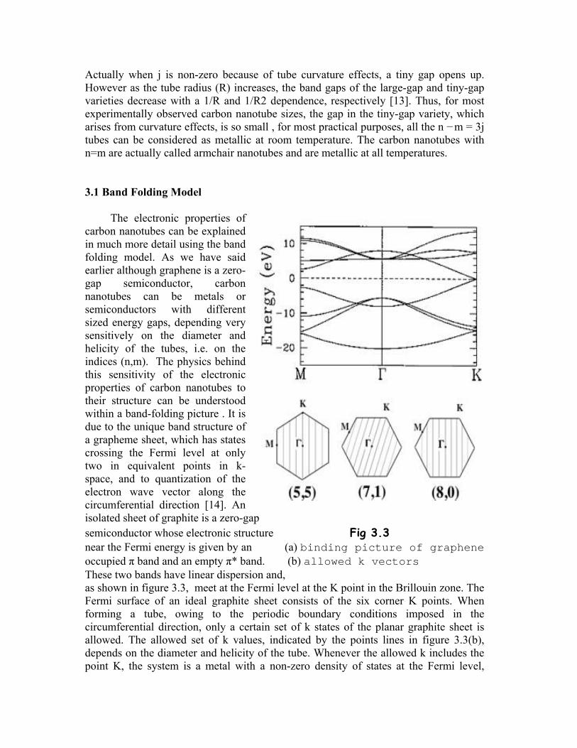
3.1 Band Folding Model The electronic properties of
carbon nanotubes can be explained in much more detail using the band folding model. As we have said earlier although graphene is a zero-gap semiconductor, carbon nanotubes can be metals or semiconductors with different sized energy gaps, depending very sensitively on the diameter and helicity of the tubes, i.e. on the indices (n,m). The physics behind this sensitivity of the electronic properties of carbon nanotubes to their structure can be understood within a band-folding picture . It is due to the unique band structure of a grapheme sheet, which has states crossing the Fermi level at only two in equivalent points in k-space, and to quantization of the electron wave vector along the circumferential direction [14]. An isolated sheet of graphite is a zero-gap semiconductor whose electronic structure Fig 3.3 near the Fermi energy is given by an (a) binding picture of graphene occupied π band and an empty π* band. (b) allowed k vectors These two bands have linear dispersion and, as shown in figure 3.3, meet at the Fermi level at the K point in the Brillouin zone. The Fermi surface of an ideal graphite sheet consists of the six corner K points. When forming a tube, owing to the periodic boundary conditions imposed in the circumferential direction, only a certain set of k states of the planar graphite sheet is allowed. The allowed set of k values, indicated by the points lines in figure 3.3(b), depends on the diameter and helicity of the tube. Whenever the allowed k includes the point K, the system is a metal with a non-zero density of states at the Fermi level,

resulting in a 1D metal with two linear dispersing bands [14]. When the point K is not included, the system is a semiconductor with different sized energy gaps. It is important to note that the states near the Fermi energy in both the metallic and the semi conducting tubes are all from states near the K point, and hence their transport and other electronic properties are related to the properties of the states on the allowed lines. For example, the conduction band and valence bands of a semi conducting tube come from states along the line closest to the K point.
3.2 Electronic Properties Of Small Diameter Carbon Nanotubes
Such a band-folding picture, based on the tight-binding approach, is expected to be valid for larger-diameter tubes. Ab initio pseudo potential local density functional calculations indeed reveal that sufficiently strong hybridization effects can occur in small-diameter nanotubes which significantly alter their electronic structure. Strongly modified low-lying conduction band states are introduced into the band gap of insulating tubes because of hybridization of the σ∗ and π∗ states . As a result, the energy gaps of some small-diameter tubes are decreased by more than 50% [15]. For example, the (6,0) tube which is predicted to be semi conducting in the band-folding scheme is shown to be metallic. However, for nanotubes with diameters greater than 1 nm, this rehybridization σ - π effects is unimportant. Recently, ultra-small-diameter single walled nanotubes (diameter ~0.4 nm) have been produced by confining their synthesis inside inert AlPO4-5 zeolite channels (with inner diameter of ca. 0.73 nm). The ultra-small diameter of these tubes has been known to give them many unusual properties, such as superconductivity.
.
3.3 Defects in Carbon Nanotubes Defects like pentagons and heptagons which could be caused by ozone treatment, Ar-ion beam irradiation , alpha-particle irradiation and electron beam irradiation are found to modify the electronic properties of these nanosystems drastically [16]. The introduction of defects into the carbon network is thus an interesting way to tailor its intrinsic properties, in order to create new potential nanodevices and to propose new potential applications in nano -electronics.
• • Fig 3.4 shows a illustration of a (9,0)-(5,5) knee which is an intra
molecular carbon nanotube junction using an heptagon–pentagon pair. This could be seen as the starting step in the fabrication of a nanodiode.
3.4 Carbon Nanotubes as Quantum Wires
Since 1992, when the electrical conductivity of carbon nanotubes was first established, several people tried to study the nature of conductivity in carbon nanotubes. In 1997 a

major breakthrough was achieved when R.Smalley et al. [17] showed that carbon nanotubes could act as quantum wires. A quantum wire is an electrically conducting wire in which quantum effects are affecting transport properties. Due to the confinement of conduction electrons in the transverse direction of the wire, their transverse energy is quantized into a series of discrete values E0 E1 and so on, where E0 refers to the lowest energy level. One consequence of this quantization is that the resistance of a quantum wire cannot be deduced from Ohm's law.
Instead an exact calculation of the transverse energies of the confined electrons has to be performed to calculate the wire resistance. Following from the quantization of electron energy, the resistance is also found to be quantized in the case of a single carbon nanotube conductance. Following this Frank et al. [18] showed that the conductance values of a single carbon nanotube is quantized as multiples of G0 (approximately 7.75 e-05 ohm-1 ) where,
G0 = 2e2/h
Where e=charge of the electron and h=plank's constant.
The most important observation here, with respect to commercial applications is that resistance is independent of length. Also carbon nanotubes are better electrical conductors due to their higher mobility and are also lighter and more compact. It has been claimed that it is possible to create macroscopic quantum wires. With a rope of carbon nanotubes, it is not necessary for any single fiber to travel the entire length, since quantum tunneling will allow electrons to jump from strand to strand.
In April 2005, NASA invested $11 million over four years with Rice University to develop quantum wire with 10 times better conductivity than copper at one-sixth the weight. It would be made with carbon nanotubes and would help reduce the weight of the next generation shuttle but can have wide ranging applications.
Fig 3.5 shows the experimental setup used by Frank et al. They varied the depth of contact between metal and nanotubes and measured the corresponding currents for a given voltage. They observed that the conductance was always a multiple of G0. Fig 3.6 shows the results of a similar experiment on three different SWNTs
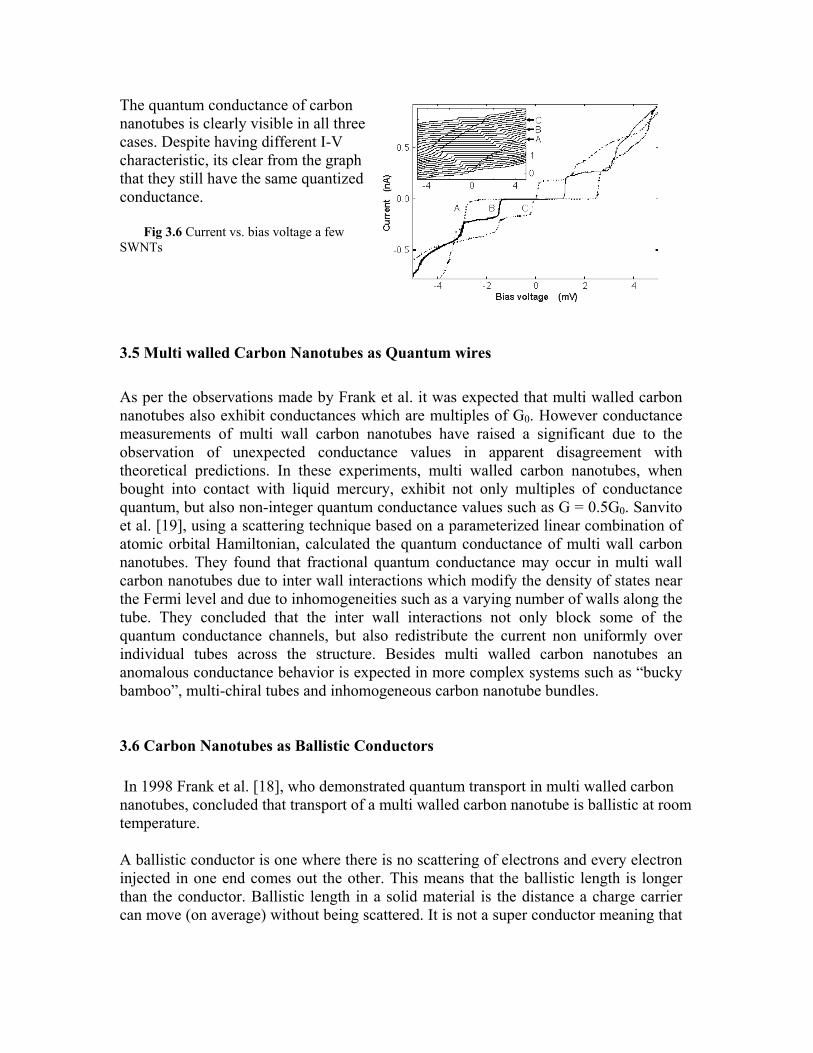
The quantum conductance of carbon nanotubes is clearly visible in all three cases. Despite having different I-V characteristic, its clear from the graph that they still have the same quantized conductance.
Fig 3.6 Current vs. bias voltage a few
SWNTs
3.5 Multi walled Carbon Nanotubes as Quantum wires
As per the observations made by Frank et al. it was expected that multi walled carbon nanotubes also exhibit conductances which are multiples of G0. However conductance measurements of multi wall carbon nanotubes have raised a significant due to the observation of unexpected conductance values in apparent disagreement with theoretical predictions. In these experiments, multi walled carbon nanotubes, when bought into contact with liquid mercury, exhibit not only multiples of conductance quantum, but also non-integer quantum conductance values such as G = 0.5G0. Sanvito et al. [19], using a scattering technique based on a parameterized linear combination of atomic orbital Hamiltonian, calculated the quantum conductance of multi wall carbon nanotubes. They found that fractional quantum conductance may occur in multi wall carbon nanotubes due to inter wall interactions which modify the density of states near the Fermi level and due to inhomogeneities such as a varying number of walls along the tube. They concluded that the inter wall interactions not only block some of the quantum conductance channels, but also redistribute the current non uniformly over individual tubes across the structure. Besides multi walled carbon nanotubes an anomalous conductance behavior is expected in more complex systems such as “bucky bamboo”, multi-chiral tubes and inhomogeneous carbon nanotube bundles.
3.6 Carbon Nanotubes as Ballistic Conductors In 1998 Frank et al. [18], who demonstrated quantum transport in multi walled carbon nanotubes, concluded that transport of a multi walled carbon nanotube is ballistic at room temperature. A ballistic conductor is one where there is no scattering of electrons and every electron injected in one end comes out the other. This means that the ballistic length is longer than the conductor. Ballistic length in a solid material is the distance a charge carrier can move (on average) without being scattered. It is not a super conductor meaning that
there is nonzero resistance, but generally the resistances of materials demonstrating ballistic conduction also have very low resistivities. Heer et al. [20] demonstrated that the intrinsic resistance of clean arc - produced carbon nanotubes is at most 200 ohms/μm, which implies that the momentum mean free path is greater than 30 μ m, which in turn is larger than the tube lengths that can be produced. This implies that these tubes are ballistic, according to the standard definition of ballistic transport.
Though these may seem like very small lengths these wires are of ideal length at which connecting wires would be required in electronic circuits as in a processor in the near future. Also it has been claimed that it is possible to create macroscopic quantum wires. With a rope of carbon nanotubes, it is not necessary for any single fiber to travel the entire length, since quantum tunneling will allow electrons to jump from strand to strand. This way it would be possible to make ballistic conductors of any length. 4. CNT Devices
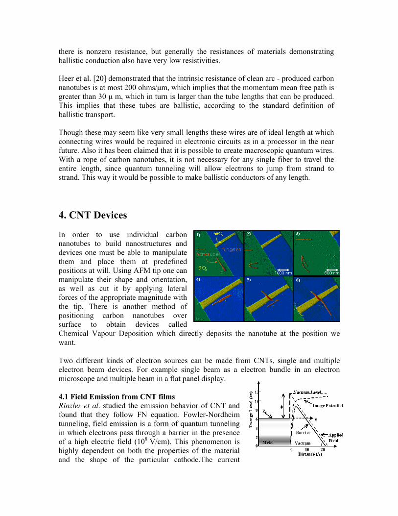
In order to use individual carbon nanotubes to build nanostructures and devices one must be able to manipulate them and place them at predefined positions at will. Using AFM tip one can manipulate their shape and orientation, as well as cut it by applying lateral forces of the appropriate magnitude with the tip. There is another method of positioning carbon nanotubes over surface to obtain devices called Chemical Vapour Deposition which directly deposits the nanotube at the position we want.
Two different kinds of electron sources can be made from CNTs, single and multiple electron beam devices. For example single beam as a electron bundle in an electron microscope and multiple beam in a flat panel display.
4.1 Field Emission from CNT films Rinzler et al. studied the emission behavior of CNT and found that they follow FN equation. Fowler-Nordheim tunneling, field emission is a form of quantum tunneling in which electrons pass through a barrier in the presence of a high electric field (108 V/cm). This phenomenon is highly dependent on both the properties of the material and the shape of the particular cathode.The current
density produced by a given electric field is governed by the Fowler-Nordheim equation.
I = aV2exp(−bφ3/2/βV )
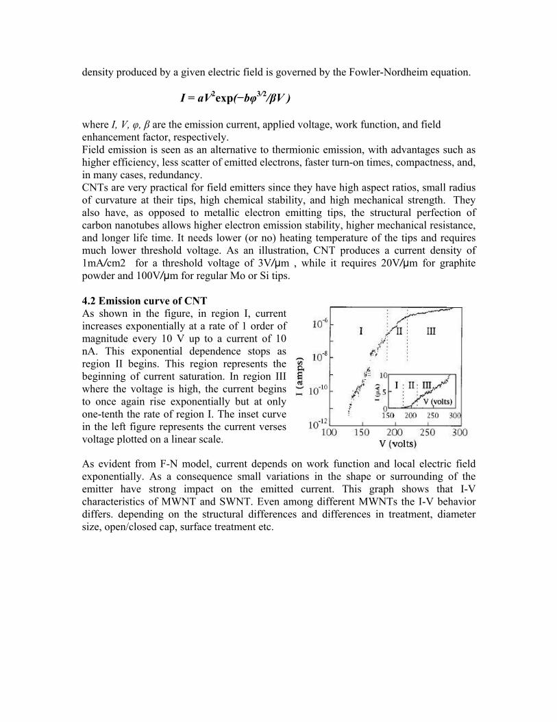
where I, V, φ, β are the emission current, applied voltage, work function, and field enhancement factor, respectively. Field emission is seen as an alternative to thermionic emission, with advantages such as higher efficiency, less scatter of emitted electrons, faster turn-on times, compactness, and, in many cases, redundancy. CNTs are very practical for field emitters since they have high aspect ratios, small radius of curvature at their tips, high chemical stability, and high mechanical strength. They also have, as opposed to metallic electron emitting tips, the structural perfection of carbon nanotubes allows higher electron emission stability, higher mechanical resistance, and longer life time. It needs lower (or no) heating temperature of the tips and requires much lower threshold voltage. As an illustration, CNT produces a current density of 1mA/cm2 for a threshold voltage of 3V/μm , while it requires 20V/μm for graphite powder and 100V/μm for regular Mo or Si tips. 4.2 Emission curve of CNT As shown in the figure, in region I, current increases exponentially at a rate of 1 order of magnitude every 10 V up to a current of 10 nA. This exponential dependence stops as region II begins. This region represents the beginning of current saturation. In region III where the voltage is high, the current begins to once again rise exponentially but at only one-tenth the rate of region I. The inset curve in the left figure represents the current verses voltage plotted on a linear scale. As evident from F-N model, current depends on work function and local electric field exponentially. As a consequence small variations in the shape or surrounding of the emitter have strong impact on the emitted current. This graph shows that I-V characteristics of MWNT and SWNT. Even among different MWNTs the I-V behavior differs. depending on the structural differences and differences in treatment, diameter size, open/closed cap, surface treatment etc.
4.3 Transistor With the silicon technology pushed to its limits, the new material to make smaller and efficient semiconductor devices was largely felt. At smaller dimensions, problems like overheating, insufficient carrier density have to be handled. There is also limit caused by the minimum wavelength of light used in lithographic techniques used for integrated circuit production nowadays. A major step in downscaling would be the application of single molecules in electronic devices. The nanotube the most promising candidate for this because of their unique properties and size. Transistors are the basic building blocks of any integrated circuits . A transistor is a three terminal device which produces an output (ON) only if a voltage above threshold is applied at gate otherwise the device is OFF.
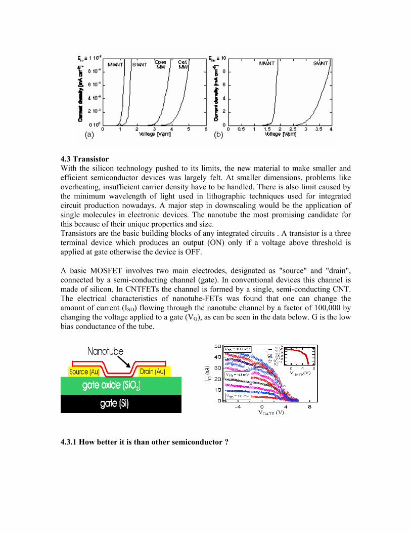
A basic MOSFET involves two main electrodes, designated as "source" and "drain", connected by a semi-conducting channel (gate). In conventional devices this channel is made of silicon. In CNTFETs the channel is formed by a single, semi-conducting CNT. The electrical characteristics of nanotube-FETs was found that one can change the amount of current (ISD) flowing through the nanotube channel by a factor of 100,000 by changing the voltage applied to a gate (VG), as can be seen in the data below. G is the low bias conductance of the tube.
4.3.1 How better it is than other semiconductor ?
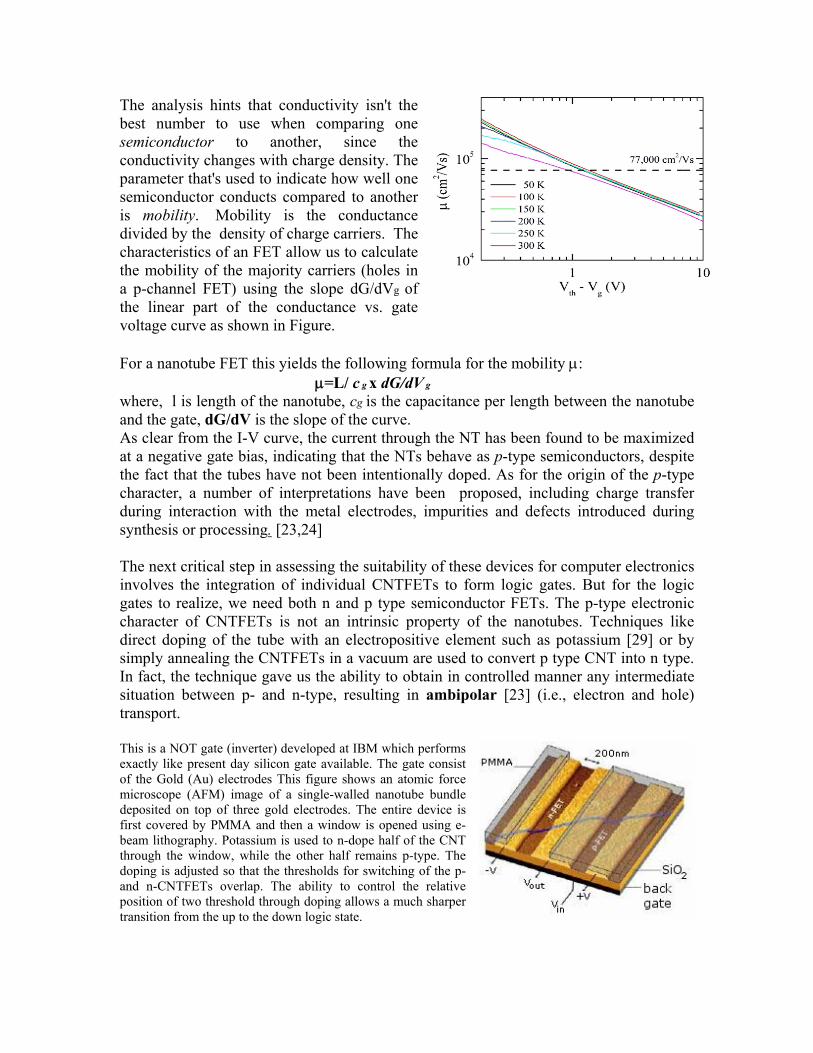
The analysis hints that conductivity isn't the best number to use when comparing one semiconductor to another, since the conductivity changes with charge density. The parameter that's used to indicate how well one semiconductor conducts compared to another is mobility. Mobility is the conductance divided by the density of charge carriers. The characteristics of an FET allow us to calculate the mobility of the majority carriers (holes in a p-channel FET) using the slope dG/dVg of the linear part of the conductance vs. gate voltage curve as shown in Figure. For a nanotube FET this yields the following formula for the mobility μ:
μ=L/ c g x dG/dV g
where, l is length of the nanotube, cg is the capacitance per length between the nanotube and the gate, dG/dV is the slope of the curve.
As clear from the I-V curve, the current through the NT has been found to be maximized at a negative gate bias, indicating that the NTs behave as p-type semiconductors, despite the fact that the tubes have not been intentionally doped. As for the origin of the p-type character, a number of interpretations have been proposed, including charge transfer during interaction with the metal electrodes, impurities and defects introduced during synthesis or processing. [23,24] The next critical step in assessing the suitability of these devices for computer electronics involves the integration of individual CNTFETs to form logic gates. But for the logic gates to realize, we need both n and p type semiconductor FETs. The p-type electronic character of CNTFETs is not an intrinsic property of the nanotubes. Techniques like direct doping of the tube with an electropositive element such as potassium [29] or by simply annealing the CNTFETs in a vacuum are used to convert p type CNT into n type. In fact, the technique gave us the ability to obtain in controlled manner any intermediate situation between p- and n-type, resulting in ambipolar [23] (i.e., electron and hole) transport.
This is a NOT gate (inverter) developed at IBM which performs exactly like present day silicon gate available. The gate consist of the Gold (Au) electrodes This figure shows an atomic force microscope (AFM) image of a single-walled nanotube bundle deposited on top of three gold electrodes. The entire device is first covered by PMMA and then a window is opened using e-beam lithography. Potassium is used to n-dope half of the CNT through the window, while the other half remains p-type. The doping is adjusted so that the thresholds for switching of the p- and n-CNTFETs overlap. The ability to control the relative position of two threshold through doping allows a much sharper transition from the up to the down logic state.
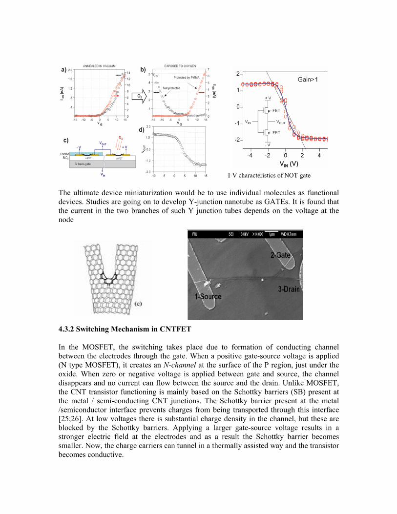
I-V characteristics of NOT gate
The ultimate device miniaturization would be to use individual molecules as functional devices. Studies are going on to develop Y-junction nanotube as GATEs. It is found that the current in the two branches of such Y junction tubes depends on the voltage at the node
4.3.2 Switching Mechanism in CNTFET
In the MOSFET, the switching takes place due to formation of conducting channel between the electrodes through the gate. When a positive gate-source voltage is applied (N type MOSFET), it creates an N-channel at the surface of the P region, just under the oxide. When zero or negative voltage is applied between gate and source, the channel disappears and no current can flow between the source and the drain. Unlike MOSFET, the CNT transistor functioning is mainly based on the Schottky barriers (SB) present at the metal / semi-conducting CNT junctions. The Schottky barrier present at the metal /semiconductor interface prevents charges from being transported through this interface [25;26]. At low voltages there is substantial charge density in the channel, but these are blocked by the Schottky barriers. Applying a larger gate-source voltage results in a stronger electric field at the electrodes and as a result the Schottky barrier becomes smaller. Now, the charge carriers can tunnel in a thermally assisted way and the transistor becomes conductive.
With the use of CNT as gates the density of gates can be reduced drastically, allowing more dense packing. Moreover there is advantage of stability and mobility. Because of high mobility chip response will be faster taking the chip processing speed to a new height (1 TF)
4.3.3 Single Electron Transistor (SET)
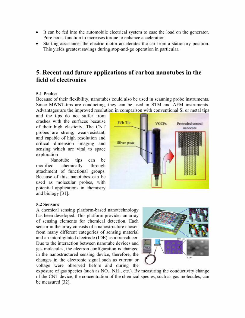
Using metal CNT as Coulomb islands CNTFET at low temperatures behaved as SET [2] Coulomb-blockade transport - whereby the Coulomb interaction between electrons can prohibit their transport around a circuit occurs in systems in which both the tunnel resistance, R, between neighboring sites is large (qh/e2) and the charging energy, EC (Ec = e2/2C, where C is the capacitance of the site), of an excess electron on a site is large compared to kT. (Here e is the charge of an electron, k is Boltzmann's constant, and h is Planck's constant.). In the blocking state no accessible energy levels are within tunneling range of the electron on the source contact. All energy levels on the island electrode with lower energies are occupied.
When a positive voltage (V>e/Q) is applied to the gate electrode the energy levels of the island electrode are lowered. The electron can tunnel onto the island, occupying a previously vacant energy level. From there it can tunnel onto the drain electrodewhere it inelastically scatters and reaches the rain electrode Fermi level. The energy levels of the island electrode are evenly spaced with a separation of ΔE. ΔE is the energy needed to each subsequent electron to the island, which acts as a self-capacitance C. The lower C the bigger ΔE gets. It is crucial for ΔE to be larger than the energy of thermal fluctuations kBT, otherwise an electron from the source electrode can always be thermally excited onto an unoccupied level of the island electrode, and no blocking can be observed. Hence it is observed that the conductance is discrete.
B T
4.3.3.1 Construction of SET
a) Chemical profiling
Schematic p-n-p nanotube device. The CNTs are doped in an uncovered region with K to make it n-type, the neighbouring regions are covered with PMMA to keep them p-doped. This p-n-p nanotube system behaves as a single QD, investigations showed that the QD are confined in the n region with the two p-n junctions as barriers for the dots. [27]

b) Bending CNTs: Cees Dekker showed the fabrication of a room temperature SET by bending a metallic SWNT with an AFM. A set consists out of a conducting island that is connected by tunneling barriers to two metallic leads. For temperatures and bias voltages that are low relative to a characteristic energy required to add an electron to the island, electrical transport through the device is blocked. Conduction is possible however by tuning a voltage on a close-by gate, this makes the device into a three terminal transistor. [28]
4.4 Diode
Another device which is sought to be made with the use of individual molecules is rectifier Diode. As seen, depending on their diameter and chirality, they are either one-dimensional metals or semiconductors. By introducing a pentagon and a heptagon into the hexagonal carbon lattice, two tube segments with different atomic and electronic structures can be seamlessly fused together to create intra molecular metal-metal, metal-semiconductor, or semiconductor-semiconductor junctions. It was found that a metal- semiconductor junction behaves like a rectifying diode with nonlinear transport characteristics that are strongly asymmetric with respect to bias polarity.
In the case of a metal-metal junction, the conductance appears to be strongly suppressed and it displays a power-law dependence on temperatures and applied voltage, consistent with tunneling between the ends of two Luttinger liquids. Above shown figure displays examples of atomic force microscope images of nanotube junction devices. Each nanotube consists of two straight segments connected by a sharp kink . In principle, such kinks can originate from two different mechanisms: a pentagon-heptagon (5-7) topological defect pair as illustrated in fig. above, or a local mechanical deformation in a uniform nanotube. Insertion of a pentagon (or heptagon) into the hexagonal carbon network creates a cap like (or saddle like) curvature leading to a kink formation. The side figures showing the Current-

voltage characteristics across the metal-semiconductor junction of CNTs showing rectifying behavior.
4.4.1 Working of the Diode
For an isolated nanotube containing an M-S junction, the Fermi energy of the metallic segment is aligned with the middle of the energy gap of the semi conducting segment. The alignment is modified when the sample is connected to metal electrodes. Owing to the higher work function for the metal, both pieces will be hole-doped by the electrodes. The difference in electronic structures and screening properties of metallic and semi conducting nanotubes will give rise to different band-bending profiles in the tube segments away from the electrodes and subsequently a Schottky-type barrier at the M-S interface, which explains the rectifying behavior across the junction. When a voltage higher than threshold is applied the barrier is overcome and the CNT allows large current to flow through it.
4.5 Ultra capacitor
Ultracapacitors or double layer capacitors (DLCs) are energy storage devices whose operation is based on the double layer effect. DLCs can achieve a energy density (6Wh/kg) much greater than the energy density of a conventional capacitor ( but far less than lithium-ion batteries-120Wh/kg). Researchers at MIT’s Laboratory for Electromagnetic and Electronic Systems (LEES) are investigating the use of nanotube structures to improve the energy storage density of ultra capacitors to a level comparable with that of NiMH batteries, while maintaining or even improving the ultra capacitors’ high performance. Researchers overcame constraints on electrode surface area and spacing problem by aligning the SWCNTs in a matrix vertically as electrode. Storage capacity in an ultra capacitor is proportional to the surface area of the electrodes. Unlike activated carbon (use for electrodes) whose pores are irregular in size and shape the vertically-aligned nanotubes have a regular shape, and a size that is only several atomic diameters in width. The result is a significantly more effective surface area, which equates to significantly increased storage capacity.
The MIT analysis shows that the CNT ultracapacitor could have an energy density higher than 60 Wh/kg, a power density greater than 100 kW/kg, and a lifetime longer than 300,000 cycles. Their thermal response is also superior to that of batteries. The new nanotube-enhanced ultracapacitors could be made in any of the sizes. It can handle very high charging currents that are impossible with a battery because of its inherently high internal impedance (major hurdle in the efficiency of device).
• It can be fed into the automobile electrical system to ease the load on the generator. Pure boost function to increases torque to enhance acceleration.
• Starting assistance: the electric motor accelerates the car from a stationary position. This yields greatest savings during stop-and-go operation in particular.
5. Recent and future applications of carbon nanotubes in the field of electronics 5.1 Probes Because of their flexibility, nanotubes could also be used in scanning probe instruments. Since MWNT-tips are conducting, they can be used in STM and AFM instruments. Advantages are the improved resolution in comparison with conventional Si or metal tips and the tips do not suffer from crashes with the surfaces because of their high elasticity. The CNT probes are strong, wear-resistant, and capable of high resolution and critical dimension imaging and sensing which are vital to space exploration
Nanotube tips can be modified chemically through attachment of functional groups. Because of this, nanotubes can be used as molecular probes, with potential applications in chemistry and biology [31]. 5.2 Sensors A chemical sensing platform-based nanotechnology has been developed. This platform provides an array of sensing elements for chemical detection. Each sensor in the array consists of a nanostructure chosen from many different categories of sensing material and an interdigitated electrode (IDE) as a transducer. Due to the interaction between nanotube devices and gas molecules, the electron configuration is changed in the nanostructured sensing device, therefore, the changes in the electronic signal such as current or voltage were observed before and during the exposure of gas species (such as NO2, NH3, etc.). By measuring the conductivity change of the CNT device, the concentration of the chemical species, such as gas molecules, can be measured [32].
5.3 Electronic bio-chips Low-cost disposable chips for rapid molecular analysis using handheld devices are ideal
r space applications. By incorporating nanoscale elements in diagnostics devices a hip will detect a specific biomarker signature with extremely
imple, low cost, but accurate methods for rapi
5.4 Motor Brushes Researchers demonstrated that the brushes can also perform as electronic micro-switches where the brush carbon nanotube bristles provide electrical connections as the brush turns
r. On a larger scale, the carbon nanotube brushes can conduct
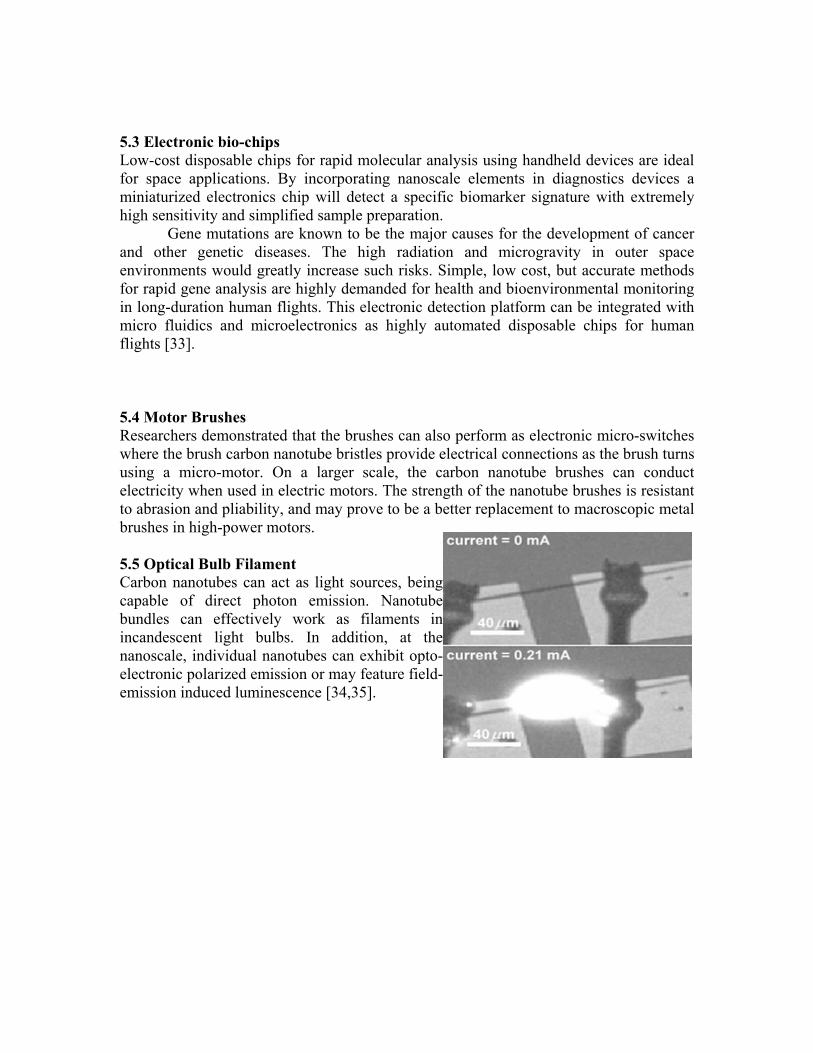
ght sources, being apable of direct photon emission. Nanotube
rk as filaments in
fominiaturized electronics chigh sensitivity and simplified sample preparation.
Gene mutations are known to be the major causes for the development of cancer and other genetic diseases. The high radiation and microgravity in outer space environments would greatly increase such risks. S
d gene analysis are highly demanded for health and bioenvironmental monitoring in long-duration human flights. This electronic detection platform can be integrated with micro fluidics and microelectronics as highly automated disposable chips for human flights [33].
using a micro-motoelectricity when used in electric motors. The strength of the nanotube brushes is resistant to abrasion and pliability, and may prove to be a better replacement to macroscopic metal brushes in high-power motors. 5.5 Optical Bulb Filament Carbon nanotubes can act as licbundles can effectively woincandescent light bulbs. In addition, at the nanoscale, individual nanotubes can exhibit opto-electronic polarized emission or may feature field-emission induced luminescence [34,35].
References
] C. Dekker, Physics Today 52, 22 (1999).
354, 56–58 (1991). . OHKOHCHI, M. WANG, S. IJIIMA, T. ICHIHASHI and Y. ANDO,
Preparation of high-grade carbon nanotubes by
gy by Bharat Bhushan.
en. ings, A. Zettl, S. Chen. A simple method for the continuous
h catalyst productivity.
nanotubes synthesized using
erene tubules metallic?, J. W. Mintmire, B. I. Dunlap and C. T. White,
9(1992)
lhaus, Phys. Rev. B 46, 1804 (1992)
, J N Wang, C T
es J.charlier 2003 Acc. Chem. Res., 35 voret, H
quantum resistors, S. Frank, P. Poncharal, Z.L. Wang, W.A. de
g, W.A. de Heer. [21] Appl. Phys. A 84, 247–250 (2006)
[1[2] Iijima, S. Nature[3] X. ZHAO, M
Hydrogen Arc Discharge. [4] Springer’s handbook of nanotechnolo[5] Noriaki Sano, Jun Nakano, Tatsuo Kanki, Synthesis of single-walled carbon nanotubes with nanohorns by arc in liquid nitrog[6] M. Ishigami, John Cumproduction of carbon nanotubes. [7] T. Guo, P. Nikolaev, A. Thess, D.T. Colbert, R.E. Smalley. Catalytic growth of single-walled nanotubes by laser vaporization. [8] Ming Su, Bo Zheng, Jie Liu. A scalable CVD method for the synthesis of single-walled carbon nanotubes with hig[9] Melissa Paradise, Tarun Goswami, Carbon nanotubes- Productions and industrial applications. [10] Matthew R. Maschmann, Placidus B. Amama, Amit Goyal, Zafar Iqbal, Timothy S. Fisher. Freestanding vertically oriented single-walled microwave plasma-enhanced CVD. [11] Are fullPhys.Rev.Lett.68,631(1992) [12] New one-dimensional conductors - graphitic microtubules, N. Hamada, S. Sawada andA.shiyama,Phys.Rev.Lett.68,157[13] Electronic structure of graphene tubules based on C60, R. Saito, M. Fujita, G. Dresselhaus and M. S. Dresse[14] Band Gap Engineering of Carbon nanotubes,Vincent H. Crespi* and Marvin L. Cohen, Physics Rev. letters 97 [15] Novel properties of 0.4 nm single-walled carbon nanotubes templated in the channels of AlPO4-5 single crystals Z K Tang, NWang, X X ZhangChan and Ping Sheng [16] Defects in Carbon Nanotub[17] Individual single-wall carbon nanotubes as quantum wires, SJ Tans, M H DeDai, A Thess, R E Smalley, L J Geerligs and C Dekker, Nature, 386, 474 [18] Carbon nanotube Heer:: Science 280, 1744 [19] Fractional quantum conductance of carbon nanotubes, S. Sanvito, C.J. Lambert, Y.-K. Kwon, D. Tománek [20] Multiwalled carbon nanotubes are ballistic conductors at room temperature C. Berger , Y. Yi, Z.L. Wan

[22] R. Martel, T. Schmidt, H. R. Shea, T. Hertel, and Ph. Avourisa) IBM Research Division, T. J. Watson Research Center, Yorktown Heights, New York
ker, Nature 393, 49-52 (1998). tel, V. Dery e, P. vouris Journal of Vacuum
Letters 80,
Applied Physics Letters 80, 73-75 (2002). 9
n pe by MinFeng Yu, Mark J. Dyer, George D. Skidmore, Henry W. Rohrs,
sm of NO2 detection in carbon nanotube field effect transistor chemical ola
i ye,Hou Tee Ng,Jie
in Sun. Applied Physics Letters 82, 1763–
5, 310. 5751, (1171 - 1174)
10598 Applied Physics Letters volume 73, number 17 [23] S. J. Tans, A. R. M. Verschueren, C. Dek[24] S. J. Wind, J. Appenzeller, R. Mar ck A , Science Technology B 20, 2798-2801 (2002). [25] Avouris, Phaedon. Molecular Electronics with Carbon Nanotubes. Accounts of Chemical Research 35(12), 1026-1034. 2002. [26] 133. V. Derycke, R. Martel, J. Appenzeller, P. Avouris, Applied Physics 2773-2775 (2002). [27]. J. Kong, J. Cao, H. J. Dai, E. Anderson,[28]. H. W. C. Postma, T. Teepen, Z. Yao, M. Grifoni, C. Dekker, Science 293, 76-7(2001). [29] V. Derycke, R. Martel, J. Appenzeller, P. Avouris, Applied Physics Letters 80, 2773-2775 (2002). [30] Zhen Yao, Henk W. Ch. Postma, Leon Balents & Cees Dekker (letter to nature) [31] Dimensional Manipulation of Carbon Nanotubes under a Scanning ElectroMicroscoXueKun Lu, Kevin D. Ausman, James R. Von Ehr, Rodney S. Ruoff.[32] Mechanisensors. Jian Zhang, Anthony Boyd, Alexander Tselev, Makarand Paranjape, and PaBarbara Appl. Phys. Lett. 88, 123112 (2006). [33] Ultrasensitive labelfree DNA analysis using electronic chip based on carbon nano electrode arrays by Jessica koehna, Hua chen,Jun li,Alan M Cassel, QHam and M.Meyyappan. [34] Polarized incandescent light emission from carbon nanotubes Peng Li, Kaili Jiang, Ming Liu, Qunqing Li and Shoushan Fan & Jial1765 (17 March 2003) [35] Bright infrared emission from electricity induced excitons in carbon nanotubes, Science, 18 November 200