cadence setup instruction apr15 - georgia institute of...
TRANSCRIPT
ECE4430-Analog IC Design
1
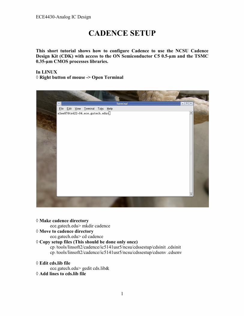
CADENCE SETUP This short tutorial shows how to configure Cadence to use the NCSU Cadence Design Kit (CDK) with access to the ON Semiconductor C5 0.5-µm and the TSMC 0.35-µm CMOS processes libraries. In LINUX ◊ Right button of mouse -> Open Terminal
◊ Make cadence directory
ece.gatech.edu> mkdir cadence ◊ Move to cadence directory
ece.gatech.edu> cd cadence ◊ Copy setup files (This should be done only once)
cp /tools/linsoft2/cadence/ic5141usr5/ncsu/cdssestup/cdsinit .cdsinit cp /tools/linsoft2/cadence/ic5141usr5/ncsu/cdssestup/cdsenv .cdsenv
◊ Edit cds.lib file ece.gatech.edu> gedit cds.lib& ◊ Add lines to cds.lib file
ECE4430-Analog IC Design
2
----------------------------------------------------------------------------------------------------------- SOFTINCLUDE $SYSTEM_CDS_LIB_DIR/cds.lib DEFINE basic $CDK_DIR/lib/basic DEFINE NCSU_Analog_Parts $CDK_DIR/lib/NCSU_Analog_Parts DEFINE NCSU_Digital_Parts $CDK_DIR/lib/NCSU_Digital_Parts DEFINE NCSU_TechLib_ami06 $CDK_DIR/lib/NCSU_TechLib_ami06 DEFINE NCSU_TechLib_tsmc04_4M2P $CDK_DIR/lib/NCSU_TechLib_tsmc04_4M2P DEFINE analogLib $CDS/tools/dfII/etc/cdslib/artist/analogLib ------------------------------------------------------------------------------------------------------------ ◊ save and quit ◊ Source > source /tools/linsoft2/cadence/ic612hf517/cshrc.meta > source /tools/linsoft2/cadence/ic612hf517/cshrc.ncsu61.lin > source /tools/linsoft2/cadence/mmsim71/cshrc.mmsim
If you edit .my-cshrc file, then you do not have to type this line always.
• How to edit my-cshrc file? o Go to root directory. (“cd”). o gedit .my-cshrc& o Add line: > source /tools/linsoft2/cadence/ic612hf517/cshrc.meta
> source /tools/linsoft2/cadence/ic612hf517/cshrc.ncsu61.lin > source /tools/linsoft2/cadence/mmsim71/cshrc.mmsim
o Save and quit o Go to cadence directory
◊ Execution cadence ece.gatech.edu> virtuoso & ◊ Tutorials Below tutorials are useful materials. http://www.eda.ncsu.edu/wiki/Tutorial:Contents � Old Tutorials
o Analog Artist Tutorial http://www.cadence.ncsu.edu/NCSUCadenceTutorial/ArtistTutorial.pdf
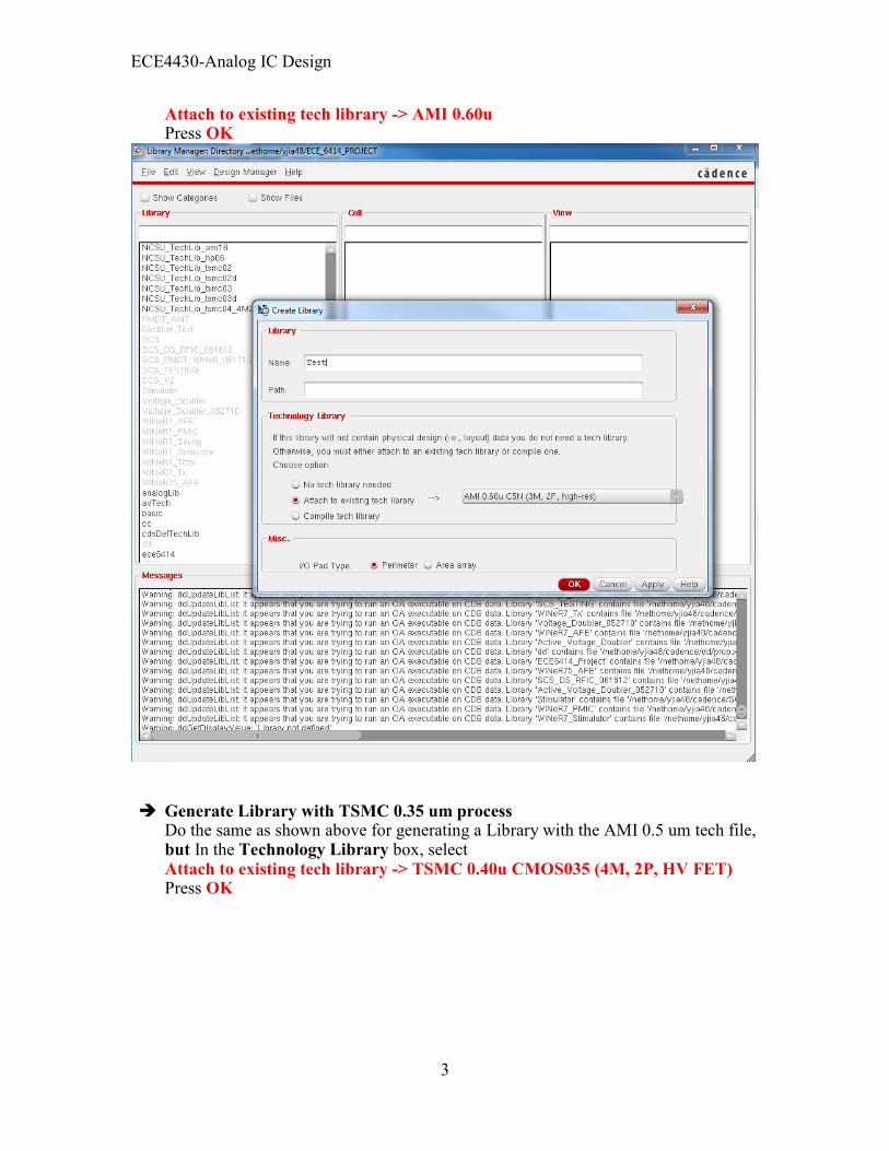
<CAUTION> You should use the tech library and transistor model files of AMI 0.60 um technology. This is different from NCSTATE tutorial. ◊ Generation of a Cadence Library with attachment to an existing technology file � Generate Library with ON Semiconductor C5 0.5-µm
In Library Manager, Click File -> New -> Library In the Name field, enter “Test” In the Technology Library box, select
ECE4430-Analog IC Design
3
Attach to existing tech library -> AMI 0.60u Press OK
� Generate Library with TSMC 0.35 um process
Do the same as shown above for generating a Library with the AMI 0.5 um tech file, but In the Technology Library box, select Attach to existing tech library -> TSMC 0.40u CMOS035 (4M, 2P, HV FET) Press OK
ECE4430-Analog IC Design
4
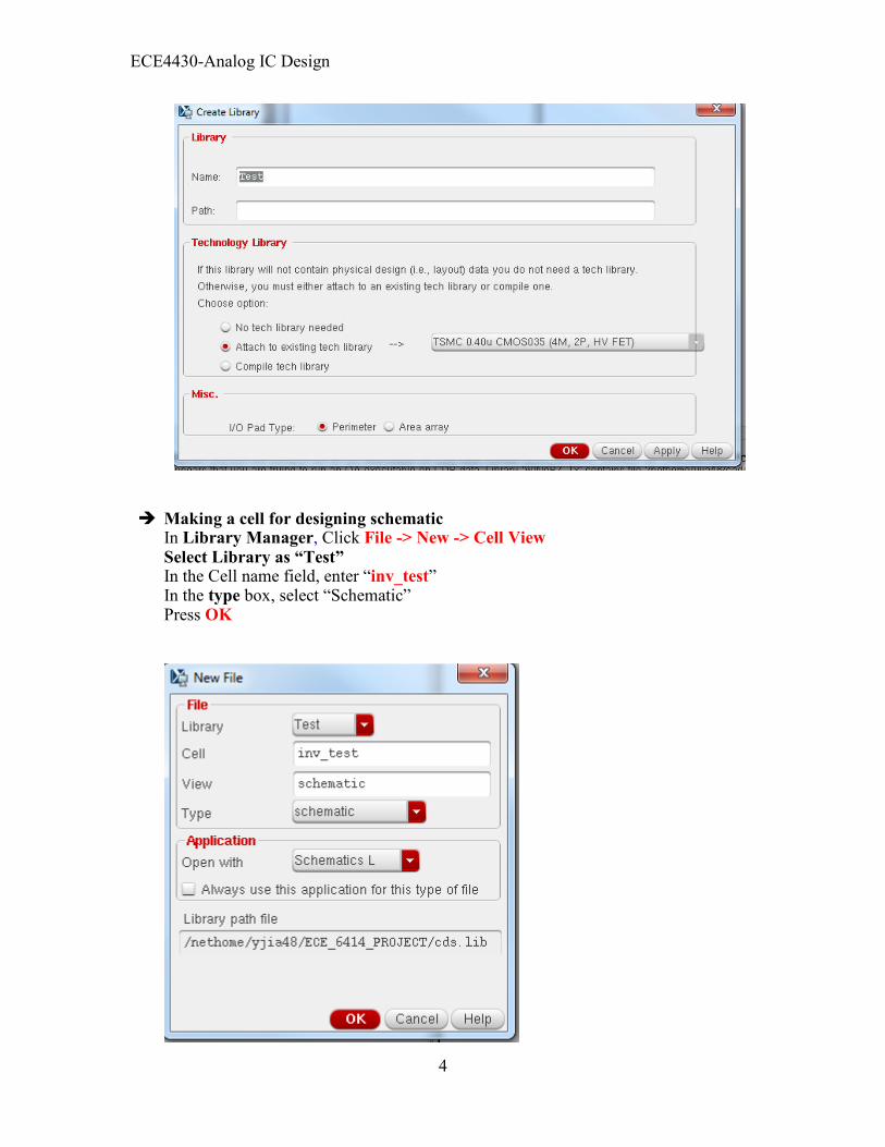
� Making a cell for designing schematic In Library Manager, Click File -> New -> Cell View Select Library as “Test” In the Cell name field, enter “inv_test” In the type box, select “Schematic” Press OK
ECE4430-Analog IC Design
5
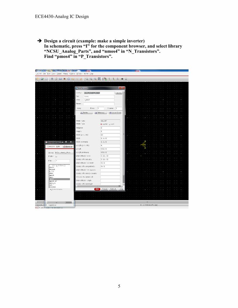
� Design a circuit (example: make a simple inverter)
In schematic, press “I” for the component browser, and select library “NCSU_Analog_Parts”, and “nmos4” in “N_Transistors”. Find “pmos4” in “P_Transistors”.
ECE4430-Analog IC Design
6
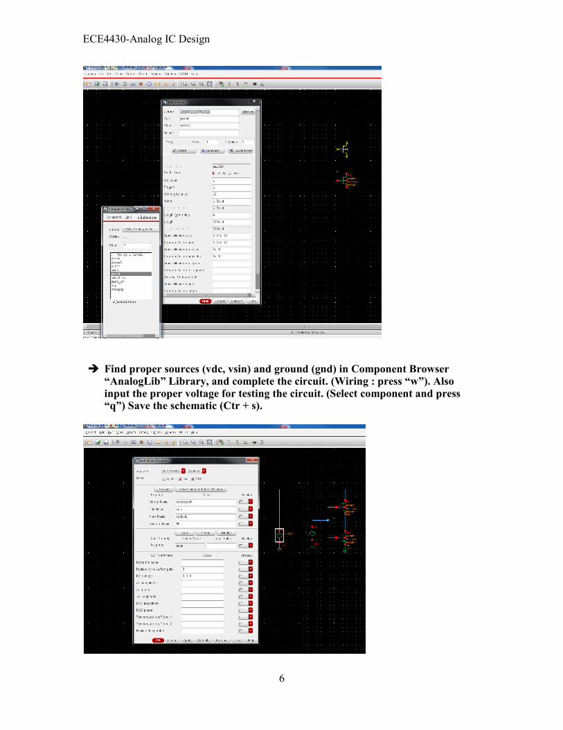
� Find proper sources (vdc, vsin) and ground (gnd) in Component Browser
“AnalogLib” Library, and complete the circuit. (Wiring : press “w”). Also input the proper voltage for testing the circuit. (Select component and press “q”) Save the schematic (Ctr + s).
ECE4430-Analog IC Design
7
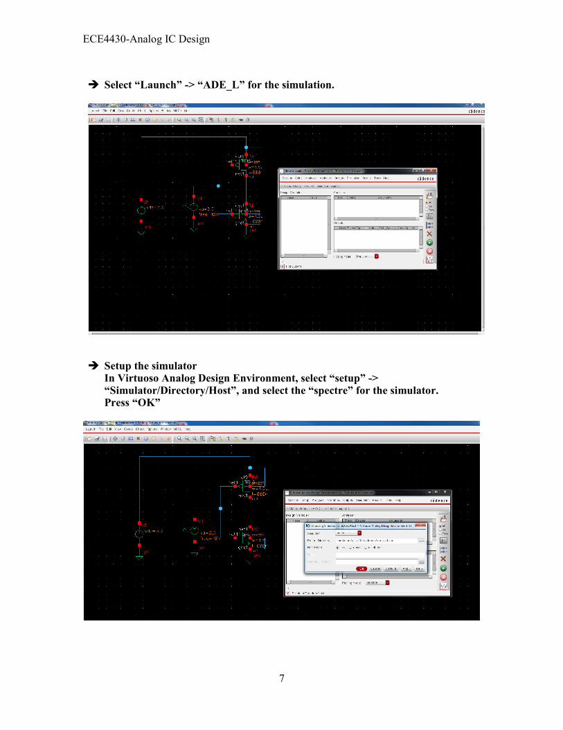
� Select “Launch” -> “ADE_L” for the simulation.
� Setup the simulator
In Virtuoso Analog Design Environment, select “setup” -> “Simulator/Directory/Host”, and select the “spectre” for the simulator. Press “OK”
ECE4430-Analog IC Design
8
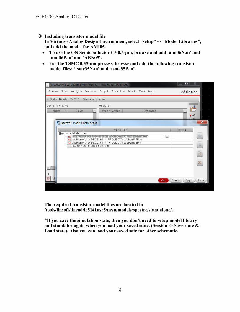
� Including transistor model file
In Virtuoso Analog Design Environment, select “setup” -> “Model Libraries”, and add the model for AMI05.
• To use the ON Semiconductor C5 0.5-µm, browse and add ‘ami06N.m’ and ‘ami06P.m’ and ‘ABN05’.
• For the TSMC 0.35-um process, browse and add the following transistor model files: ‘tsmc35N.m’ and ‘tsmc35P.m’.
The required transistor model files are located in /tools/linsoft/lincad/ic5141usr5/ncsu/models/spectre/standalone/. *If you save the simulation state, then you don’t need to setup model library and simulator again when you load your saved state. (Session -> Save state & Load state). Also you can load your saved sate for other schematic.
ECE4430-Analog IC Design
9
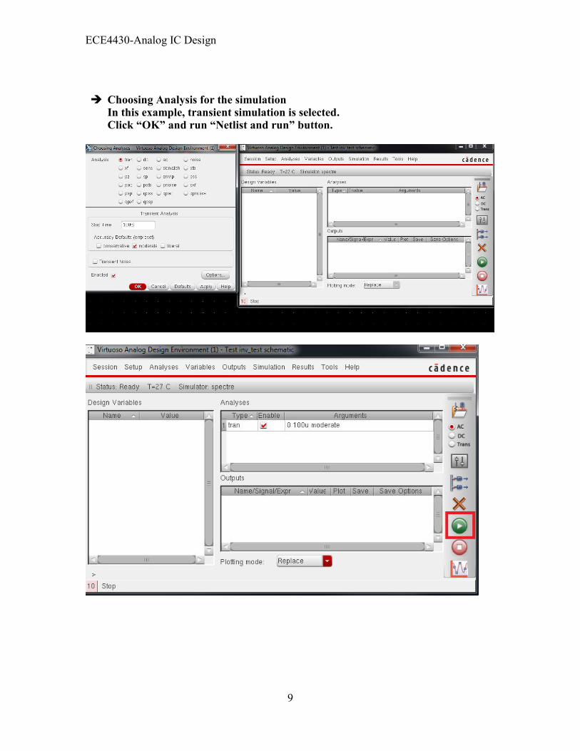
� Choosing Analysis for the simulation In this example, transient simulation is selected. Click “OK” and run “Netlist and run” button.
ECE4430-Analog IC Design
10
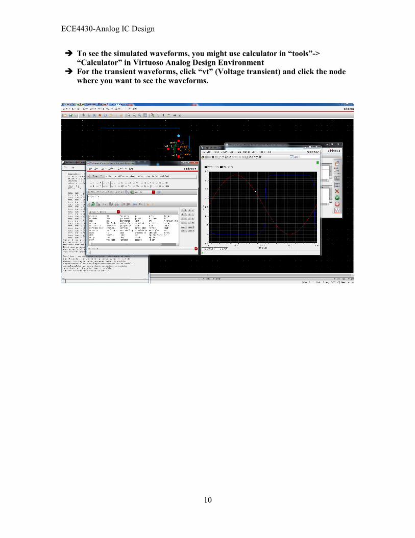
� To see the simulated waveforms, you might use calculator in “tools”-> “Calculator” in Virtuoso Analog Design Environment
� For the transient waveforms, click “vt” (Voltage transient) and click the node where you want to see the waveforms.
ECE4430-Analog IC Design
11
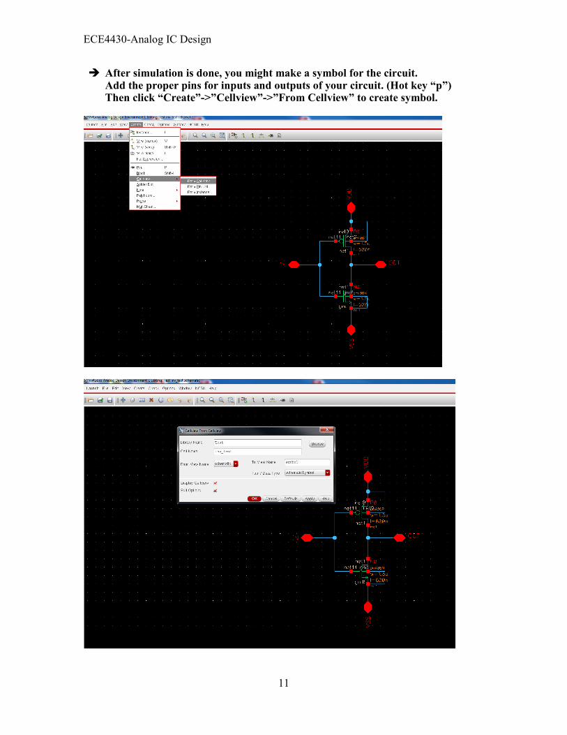
� After simulation is done, you might make a symbol for the circuit. Add the proper pins for inputs and outputs of your circuit. (Hot key “p”) Then click “Create”->”Cellview”->”From Cellview” to create symbol.
ECE4430-Analog IC Design
12
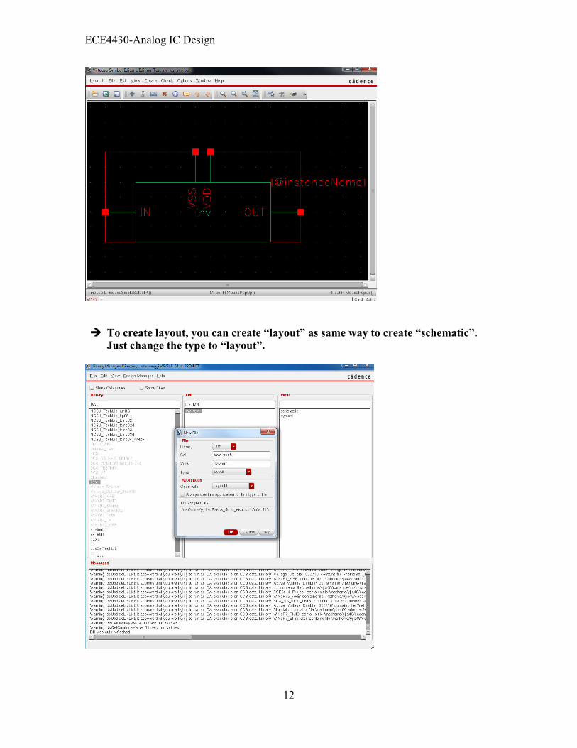
� To create layout, you can create “layout” as same way to create “schematic”.
Just change the type to “layout”.
ECE4430-Analog IC Design
13
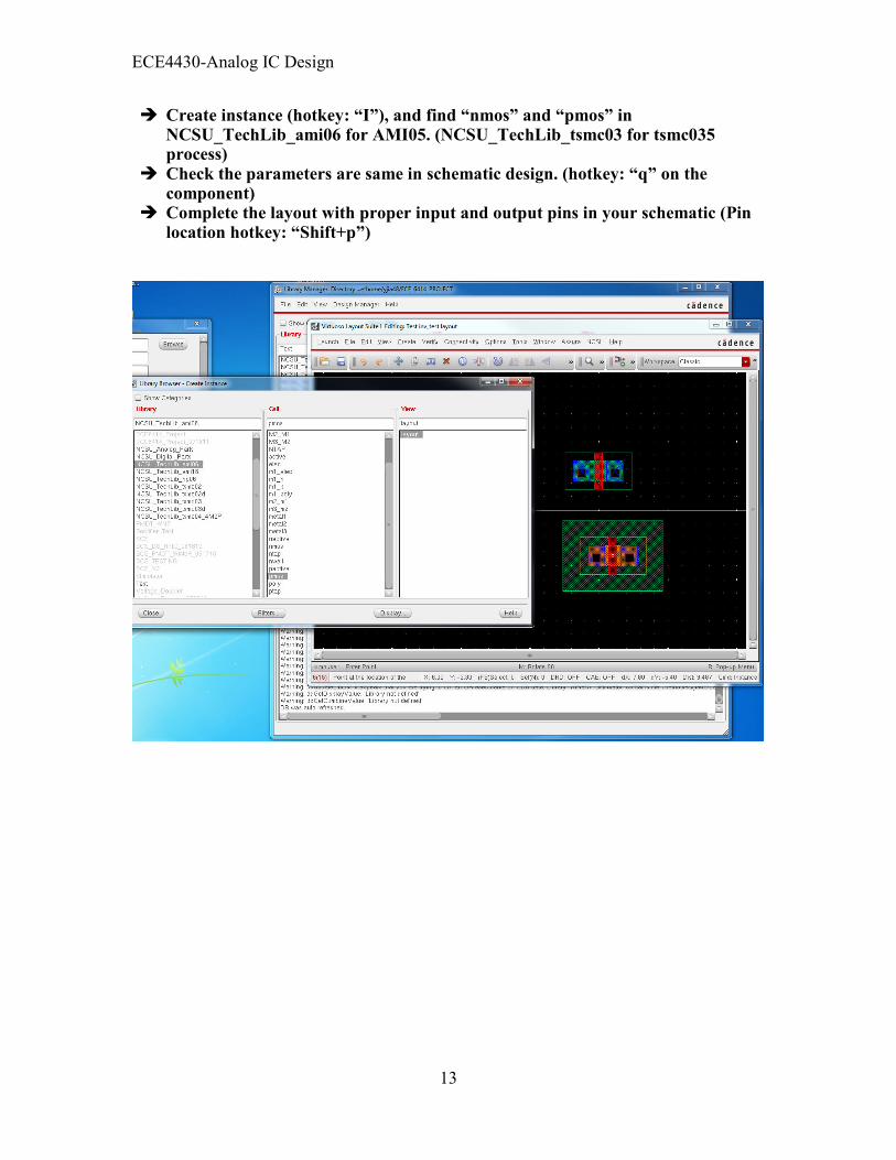
� Create instance (hotkey: “I”), and find “nmos” and “pmos” in NCSU_TechLib_ami06 for AMI05. (NCSU_TechLib_tsmc03 for tsmc035 process)
� Check the parameters are same in schematic design. (hotkey: “q” on the component)
� Complete the layout with proper input and output pins in your schematic (Pin location hotkey: “Shift+p”)
ECE4430-Analog IC Design
14
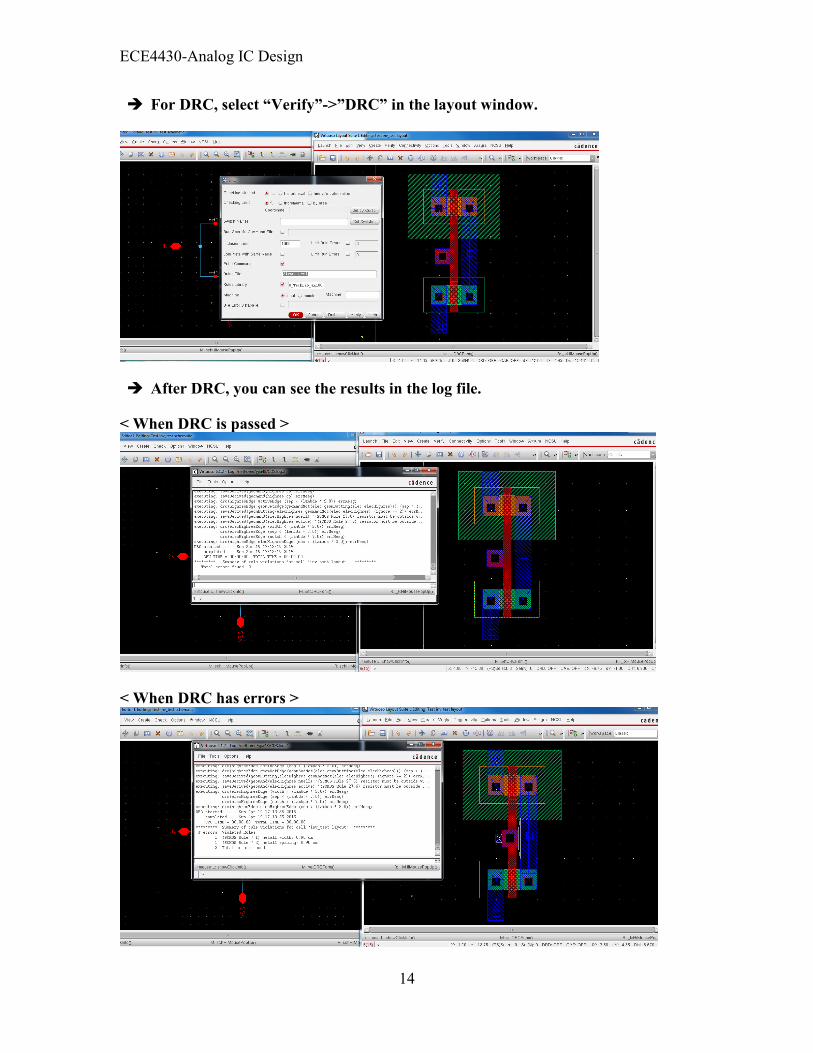
� For DRC, select “Verify”->”DRC” in the layout window.
� After DRC, you can see the results in the log file.
< When DRC is passed >
< When DRC has errors >
ECE4430-Analog IC Design
15
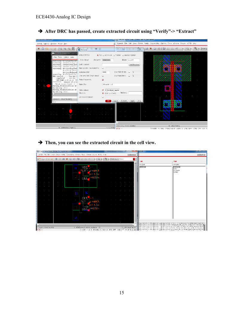
� After DRC has passed, create extracted circuit using “Verify”-> “Extract”
� Then, you can see the extracted circuit in the cell view.
ECE4430-Analog IC Design
16
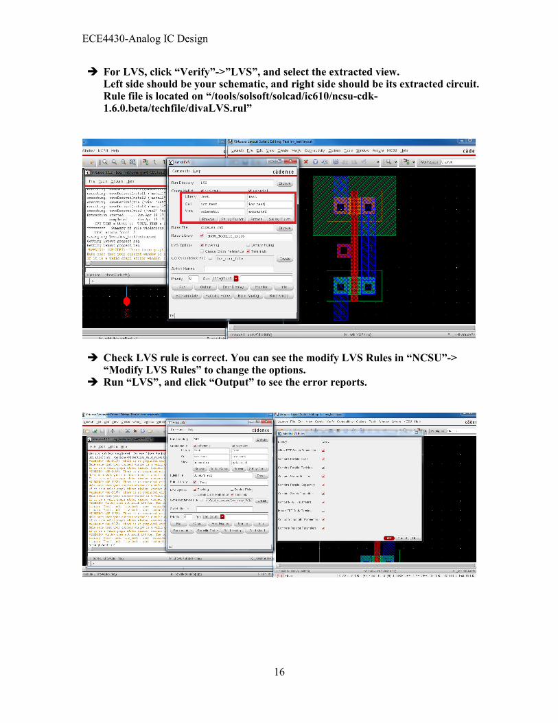
� For LVS, click “Verify”->”LVS”, and select the extracted view. Left side should be your schematic, and right side should be its extracted circuit. Rule file is located on “/tools/solsoft/solcad/ic610/ncsu-cdk-1.6.0.beta/techfile/divaLVS.rul”
� Check LVS rule is correct. You can see the modify LVS Rules in “NCSU”->
“Modify LVS Rules” to change the options. � Run “LVS”, and click “Output” to see the error reports.
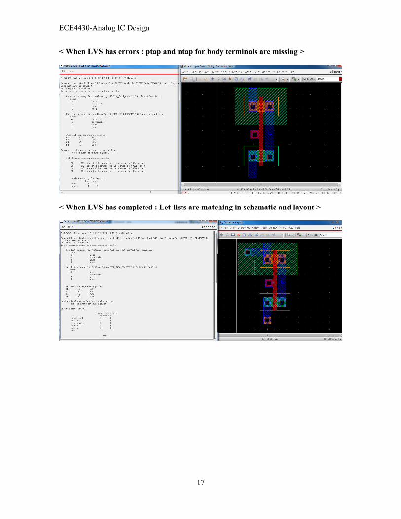
ECE4430-Analog IC Design
17
< When LVS has errors : ptap and ntap for body terminals are missing >
< When LVS has completed : Let-lists are matching in schematic and layout >