boost converter design tips - texas...
TRANSCRIPT
1
1
Boost Converter Design Tips
Alan MartinField Applications Engineering
March 2005
MODERATOR:
… National Semiconductor Online Seminar. I’m Wanda Garrett and I will be your host. Before we begin I’d like to go over the operation of your seminar interface. Slides will appear in the upper right section of your interface. If you wish like the slides to be larger, click the “Enlarge” button. Slides will automatically advance or you can click on the slide title in the list on the left to jump to that place in the presentation. At the bottom of your interface is an interactive Web browser set to a Web page containing additional resources for this seminar. Questions may be submitted at any time and the presenter will respond via email. To ask a question, click the “Ask A Question” button, then fill in the form that appears, and then submit the form. Finally, National Semiconductor owns and is responsible for all content in this seminar. Today’s topic is Boost Converter Design Tips. Today’s seminar will be given by Alan Martin, Field Applications Engineer. Welcome, Alan. Please go ahead with your seminar.

2
2
© 2003 National Semiconductor Corporation
Who should attend?
Engineers designing a boost application
Engineers and technicians getting ready to debug a boost application.
MARTIN:
Thank you, Wanda. How do you do? My name is Alan Martin. I’m a Field Applications Engineer here at National Semiconductor. I’ve been designing medium and low power switchers for nearly ten years. This seminar is intended for engineers designing a boost application and engineers and technicians getting ready to debug a boost application.

3
3
© 2003 National Semiconductor Corporation
Scope of presentation
Covering global topics that are missing from IC data sheets that relate to the design and application of boosts.
Not covering component value selectionThese are covered in the data sheets.
Several on-line simulators assist with component selection.
Give NSC WEBENCH a try!
Today we’ll be covering global topics that tend to be missing from IC datasheets that tend to relate to the application of boosts. We’re not going to be covering value selections because these are well covered in datasheets as well as in simulation packages that are available for specific ICs. We recommend you also take a look at National Semiconductor’s WEBENCH application package. There’s a Web link on one of the final slides of this presentation.
4
4
© 2003 National Semiconductor Corporation
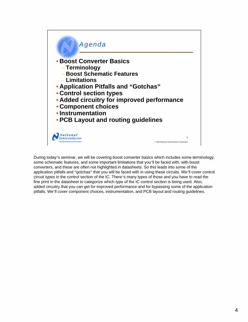
Agenda
• Boost Converter Basics– Terminology– Boost Schematic Features– Limitations
• Application Pitfalls and “Gotchas”• Control section types• Added circuitry for improved performance• Component choices• Instrumentation• PCB Layout and routing guidelines
During today’s seminar, we will be covering boost converter basics which includes some terminology, some schematic features, and some important limitations that you’ll be faced with, with boost converters, and these are often not highlighted in datasheets. So this leads into some of the application pitfalls and “gotchas” that you will be faced with in using these circuits. We’ll cover control circuit types in the control section of the IC. There’s many types of those and you have to read the fine print in the datasheet to categorize which type of the IC control section is being used. Also, added circuitry that you can get for improved performance and for bypassing some of the application pitfalls. We’ll cover component choices, instrumentation, and PCB layout and routing guidelines.
5
5
© 2003 National Semiconductor Corporation
Terminology
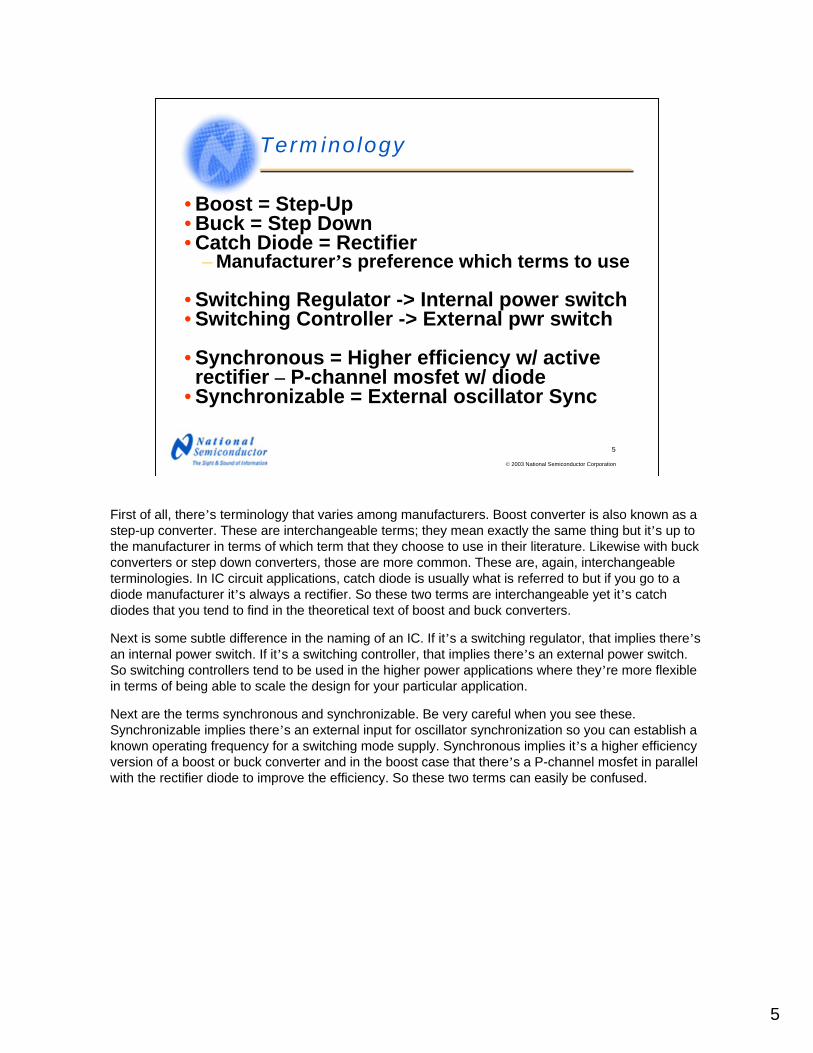
• Boost = Step-Up• Buck = Step Down • Catch Diode = Rectifier
– Manufacturer’s preference which terms to use
• Switching Regulator -> Internal power switch• Switching Controller -> External pwr switch
• Synchronous = Higher efficiency w/ active rectifier – P-channel mosfet w/ diode
• Synchronizable = External oscillator Sync
First of all, there’s terminology that varies among manufacturers. Boost converter is also known as a step-up converter. These are interchangeable terms; they mean exactly the same thing but it’s up to the manufacturer in terms of which term that they choose to use in their literature. Likewise with buck converters or step down converters, those are more common. These are, again, interchangeable terminologies. In IC circuit applications, catch diode is usually what is referred to but if you go to a diode manufacturer it’s always a rectifier. So these two terms are interchangeable yet it’s catch diodes that you tend to find in the theoretical text of boost and buck converters.
Next is some subtle difference in the naming of an IC. If it’s a switching regulator, that implies there’s an internal power switch. If it’s a switching controller, that implies there’s an external power switch. So switching controllers tend to be used in the higher power applications where they’re more flexible in terms of being able to scale the design for your particular application.
Next are the terms synchronous and synchronizable. Be very careful when you see these. Synchronizable implies there’s an external input for oscillator synchronization so you can establish a known operating frequency for a switching mode supply. Synchronous implies it’s a higher efficiency version of a boost or buck converter and in the boost case that there’s a P-channel mosfet in parallel with the rectifier diode to improve the efficiency. So these two terms can easily be confused.
6
6
© 2003 National Semiconductor Corporation
More terminology
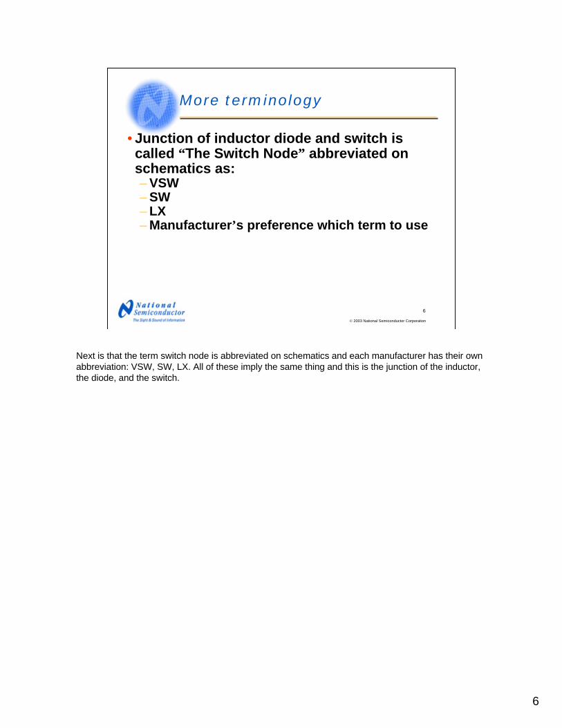
• Junction of inductor diode and switch is called “The Switch Node” abbreviated on schematics as: – VSW– SW– LX– Manufacturer’s preference which term to use
Next is that the term switch node is abbreviated on schematics and each manufacturer has their own abbreviation: VSW, SW, LX. All of these imply the same thing and this is the junction of the inductor, the diode, and the switch.
7
7
© 2003 National Semiconductor Corporation
Basic boost schematic
1
23
SwitchNodeVIN
R2
FB
COUT
GND SNS
VOUT (>VIN)
CIN
R1
Rsns
VIN
D2 1
GATE
L
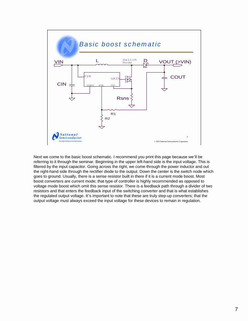
Next we come to the basic boost schematic. I recommend you print this page because we’ll be referring to it through the seminar. Beginning in the upper left-hand side is the input voltage. This is filtered by the input capacitor. Going across the right, we come through the power inductor and out the right-hand side through the rectifier diode to the output. Down the center is the switch node which goes to ground. Usually, there is a sense resistor built in there if it is a current mode boost. Most boost converters are current mode; that type of controller is highly recommended as opposed to voltage mode boost which omit this sense resistor. There is a feedback path through a divider of two resistors and that enters the feedback input of the switching converter and that is what establishes the regulated output voltage. It’s important to note that these are truly step-up converters; that the output voltage must always exceed the input voltage for these devices to remain in regulation.
8
8
© 2003 National Semiconductor Corporation
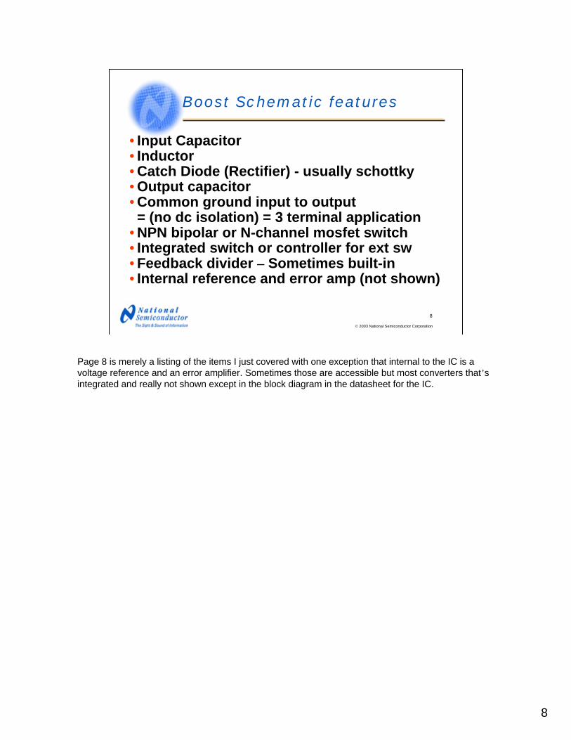
Boost Schematic features
• Input Capacitor• Inductor• Catch Diode (Rectifier) - usually schottky• Output capacitor• Common ground input to output= (no dc isolation) = 3 terminal application
• NPN bipolar or N-channel mosfet switch• Integrated switch or controller for ext sw• Feedback divider – Sometimes built-in• Internal reference and error amp (not shown)
Page 8 is merely a listing of the items I just covered with one exception that internal to the IC is a voltage reference and an error amplifier. Sometimes those are accessible but most converters that’s integrated and really not shown except in the block diagram in the datasheet for the IC.
9
9
© 2003 National Semiconductor Corporation
Other control section features sometimes available
• “Enable”• Soft start
– limits inrush current– Limits output voltage overshoot
• Compensation - RC or CRC network– Certain types of control need for stability– Sometimes internal compensation– less flexible– Certain types of control inherently stable– (May also provide extra control input for other features)
• Current sense input for current mode control• Reference voltage bypass• Built-in rectifier diode• Built-in synchronous rectifier
– Fully integrated regulators– True shutdown function
• Negative feedback input for voltage inverting configurations• Many boost ICs can be configured as Flyback, Sepic or Cúk
There are other features which may be available on a boost IC such as enable input that will cease switching activity on the IC. Soft start which are always a good idea but this is a relatively uncommon feature. This will limit the inrush current and can limit the output voltage overshoot. There are certain types of controllers which require a compensation network. This is usually a series RC network or an RC network shunted with another capacitor. These are needed for control loop stability. Often this is a place inside the IC which may be less flexible but certainly occupies less space on the board if that’s done. There are types of controllers which do not require compensation in that they’re inherently stable. Those tend to be lower performance architectures. An advantage of having a compensation pin is that it can provide an extra control input for other features.
As shown in the schematic on page 7, there may be a current sense input for current mode control assuming that this is a controller. If it’s a regulator where the switch is built-in, that sense resistor is integrated inside of the IC. Some manufacturers have a reference voltage bypass for improving the noise characteristics of the internal reference. They may build in the rectifier diode or, in fact, they may go beyond that and make a built-in synchronous rectifier. This gives much higher efficiency in that the forward-drop of the rectifier diode is shunted. That only exists in fully integrated regulators though. And this may also include a true shutdown function which we’ll be talking about.
Occasionally there are ICs which have a negative feedback input so you can put the IC in an inverting configuration such as a Cúk. And another point is that many boost ICs can be used in Flyback or Sepic or Cúk converters assuming that they have a high enough peak switch voltage.

10
10
© 2003 National Semiconductor Corporation
Boost Converter Pitfalls
• No true shutdown = output disconnect– Disable switcher and output falls to Vin, less a
diode drop.– Read data sheet fine print - Parts with true
shutdown will brag about it.– True shutdown requires an extra switch either
in series with input or output.
One of the major shortcomings of a boost converter is that they do not have true shutdown. Now, another name for true shutdown is output disconnect. In the case where you disable the switcher, there’s a direct path from Vin to Vout through the inductor and diode. So when you disable the switcher, the output voltage drops down to Vin less a diode drop. Now, if an IC does include true shutdown, they will brag about it on the datasheet and that’s something to look for in the fine print. But if you’re looking at an IC that’s similar to the schematic on page 7, it does not have true shutdown so you’ll have to either add an extra switch either in series with the input or the output. If it’s in series with the input, it could be as simple as an on/off switch.
11
11
© 2003 National Semiconductor Corporation
Simple true shutdown circuit –with pnp bipolar
GND
R1
L VOUT
FB
SwitchNode
VIN1
23
GATE
CIN1UF
R2
VIN 1
32D
2 1
COUT
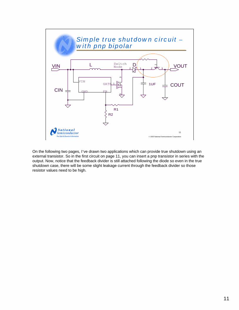
On the following two pages, I’ve drawn two applications which can provide true shutdown using an external transistor. So in the first circuit on page 11, you can insert a pnp transistor in series with the output. Now, notice that the feedback divider is still attached following the diode so even in the true shutdown case, there will be some slight leakage current through the feedback divider so those resistor values need to be high.
12
12
© 2003 National Semiconductor Corporation
Simple true shutdown circuit –with p-channel mosfet
GATE
L
FB
R2
1
32
CIN
D2 1
COUTGND
VIN
VIN
R1
1UF
VOUTSwitchNode
1
23
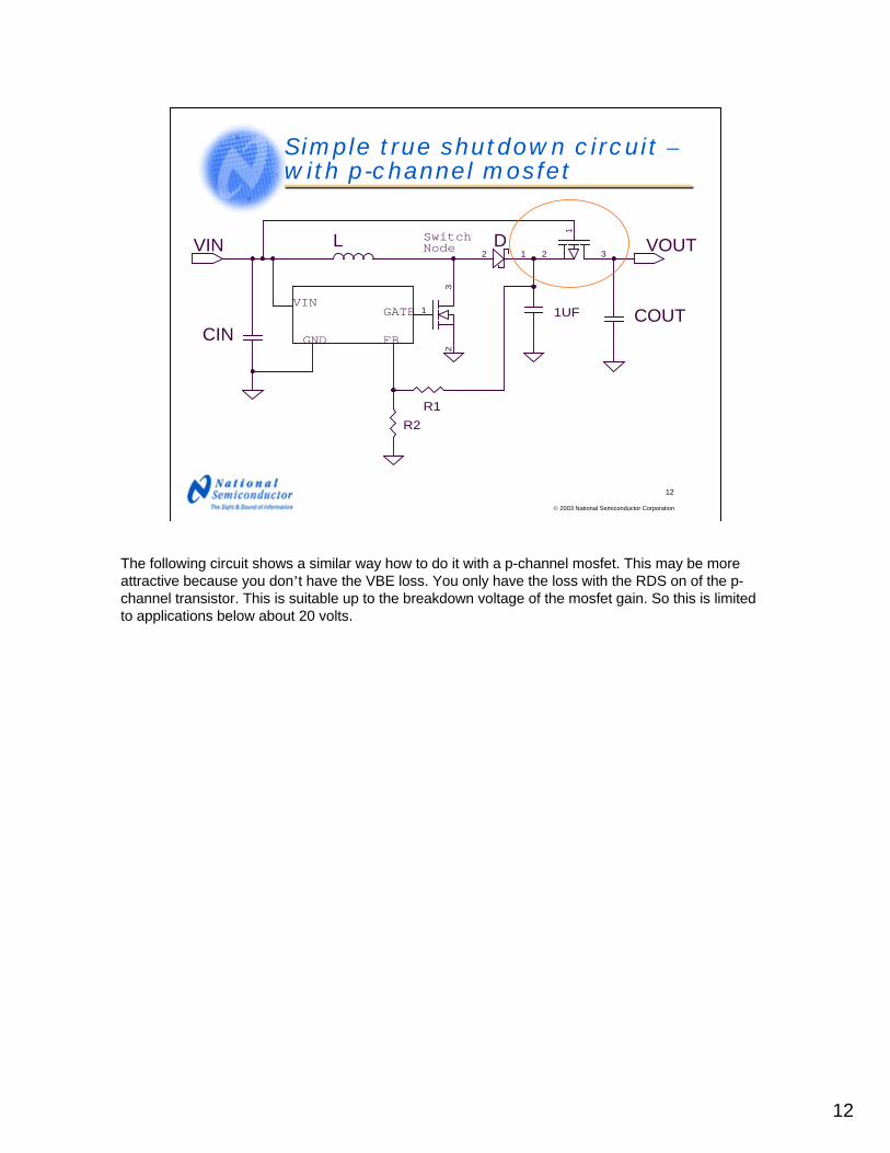
The following circuit shows a similar way how to do it with a p-channel mosfet. This may be more attractive because you don’t have the VBE loss. You only have the loss with the RDS on of the p-channel transistor. This is suitable up to the breakdown voltage of the mosfet gain. So this is limited to applications below about 20 volts.
13
13
© 2003 National Semiconductor Corporation
Simple true shutdown circuit –ac couple switch node
1
23
D22 1
FB
D1
21
L
CIN
R2
Cc VOUT
GATE
VIN
R1
GND10
COUT
SwitchNode
VIN
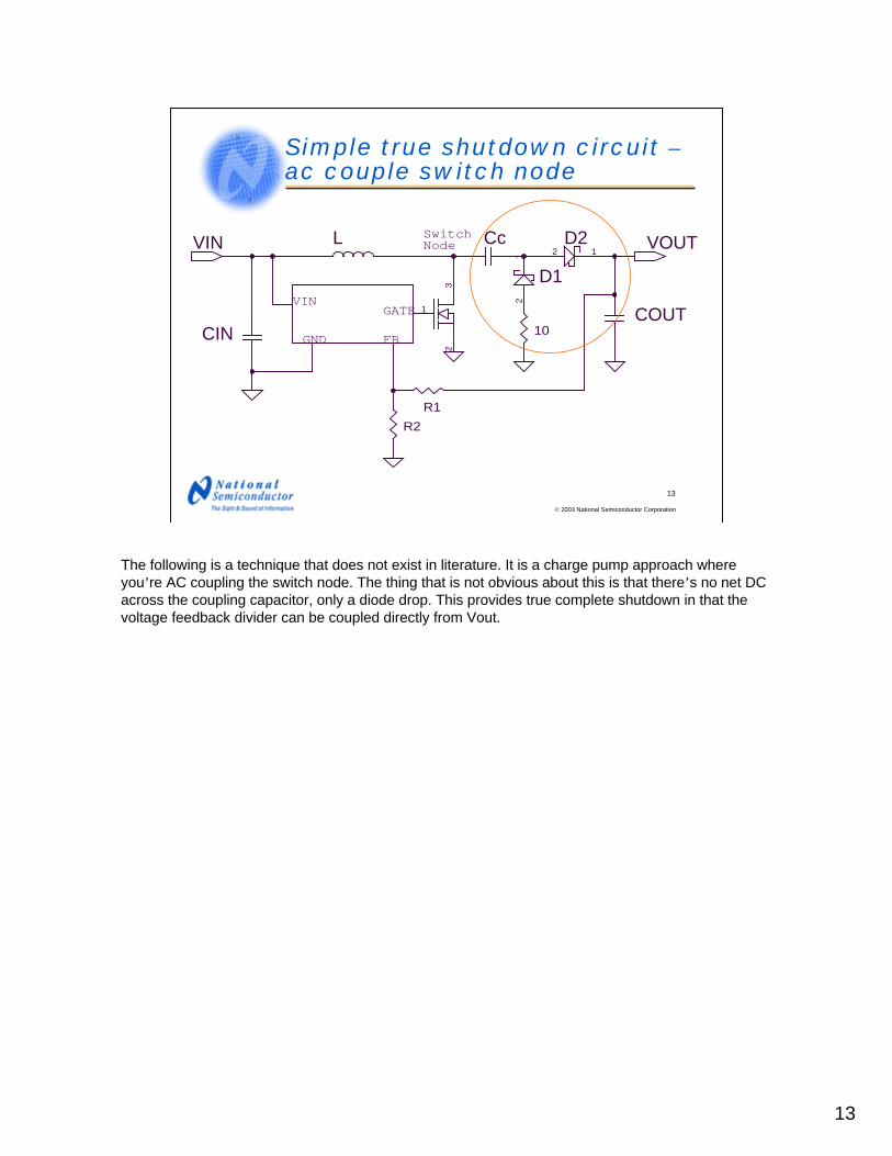
The following is a technique that does not exist in literature. It is a charge pump approach where you’re AC coupling the switch node. The thing that is not obvious about this is that there’s no net DC across the coupling capacitor, only a diode drop. This provides true complete shutdown in that the voltage feedback divider can be coupled directly from Vout.
14
14
© 2003 National Semiconductor Corporation
+/- Dual Output Supply
D22 1
10
D1
21
Cc
L
10COUT
R1
SwitchNode
D1
21
GND FB
COUT
VOUT
VIN
Cc
CIN
R2
1
23
GATE
-VOUT
D22 1
VIN
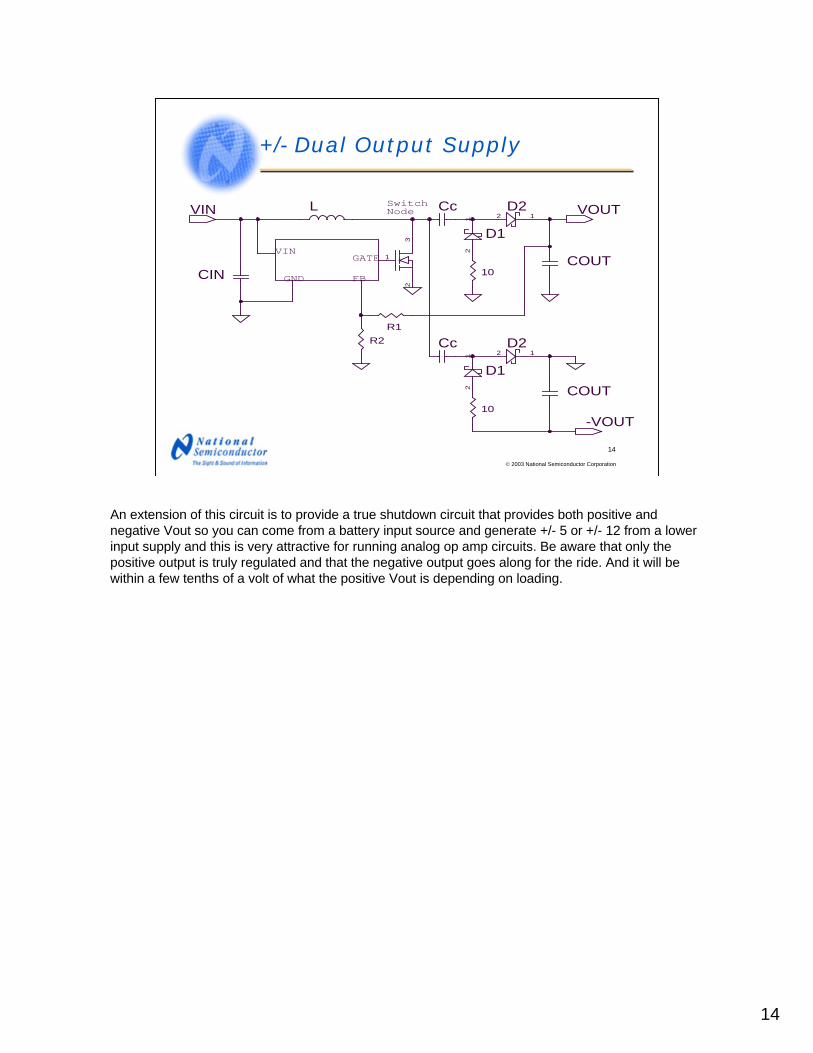
An extension of this circuit is to provide a true shutdown circuit that provides both positive and negative Vout so you can come from a battery input source and generate +/- 5 or +/- 12 from a lower input supply and this is very attractive for running analog op amp circuits. Be aware that only the positive output is truly regulated and that the negative output goes along for the ride. And it will be within a few tenths of a volt of what the positive Vout is depending on loading.
15
15
© 2003 National Semiconductor Corporation
Boost Converter Pitfalls
• No current limit on output– Uncontrolled path from Vin to Vout– Even when IC is in shutdown– Output short passes to input.– A short term short on Vout or switch can
cause over voltage damage to switch. Use care when probing with test leads!
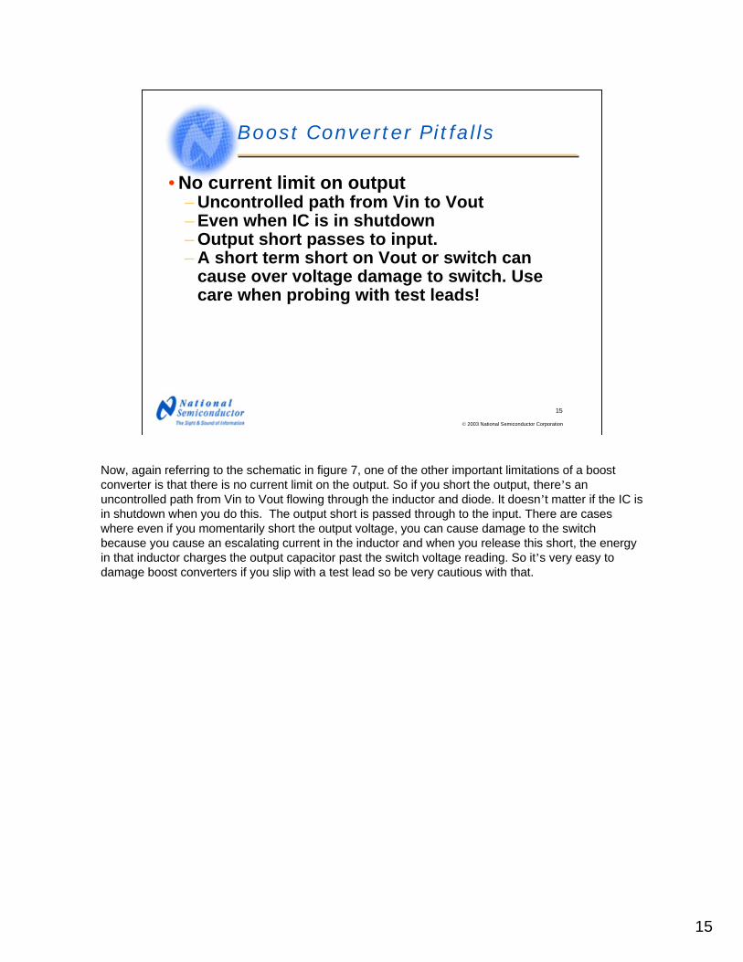
Now, again referring to the schematic in figure 7, one of the other important limitations of a boost converter is that there is no current limit on the output. So if you short the output, there’s an uncontrolled path from Vin to Vout flowing through the inductor and diode. It doesn’t matter if the IC is in shutdown when you do this. The output short is passed through to the input. There are cases where even if you momentarily short the output voltage, you can cause damage to the switch because you cause an escalating current in the inductor and when you release this short, the energy in that inductor charges the output capacitor past the switch voltage reading. So it’s very easy to damage boost converters if you slip with a test lead so be very cautious with that.
16
16
© 2003 National Semiconductor Corporation
Overloaded boost converter
GATELOW
D2 1
L VOUT < VINVIN
R2
GND
1
23
COUT
R1
CIN FB
SwitchNode
VIN
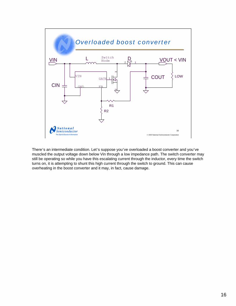
There’s an intermediate condition. Let’s suppose you’ve overloaded a boost converter and you’ve muscled the output voltage down below Vin through a low impedance path. The switch converter may still be operating so while you have this escalating current through the inductor, every time the switch turns on, it is attempting to shunt this high current through the switch to ground. This can cause overheating in the boost converter and it may, in fact, cause damage.
17
17
© 2003 National Semiconductor Corporation
More boost converter pitfalls
• Input voltage surges pass through to output– As Vin rises up to Vout ( a regulated voltage
level), the switcher stops switching. Vinpasses through inductor and diode to Vout.
• No input-output isolation – Look at flybackconverter with opto-isolated feedback if you need isolation.
Another important point is that as the input voltage surges, that this will be passed through to the output. So as Vin rises up past the regulated Voutput voltage level, the switcher stops switching and Vin passes through the inductor and the diode to Vout. So there – you can cause damage to your load circuitry if there’s an input surge occurring. Another shortcoming is that there’s no isolation between input and output. This is a three terminal connection. Circuitry input and output grounds are common. If you need an isolated converter where there’s no DC continuity between input and output grounds, take a look at the flyback converter using opto-isolated feedback.
18
18
© 2003 National Semiconductor Corporation
Boost schematic variations: Separate VIN, Vbias
GATE
VOUT (>VIN)
0.1UF
VbiasVIN
R2
GND
1
23
VIN
FB
D2 1
COUTCIN
R1
L
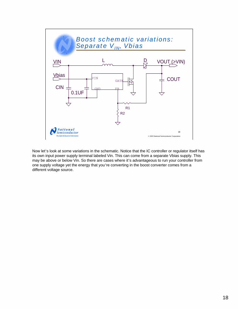
Now let’s look at some variations in the schematic. Notice that the IC controller or regulator itself has its own input power supply terminal labeled Vin. This can come from a separate Vbias supply. This may be above or below Vin. So there are cases where it’s advantageous to run your controller from one supply voltage yet the energy that you’re converting in the boost converter comes from a different voltage source.
19
19
© 2003 National Semiconductor Corporation
Boost schematic variations: Vbias bootstrapped from VOUT
CIN
R1
0.1UF
COUT
GND
VOUT (>VIN)
GATE
R2
L
VIN
FB
D2 1VIN
1
23
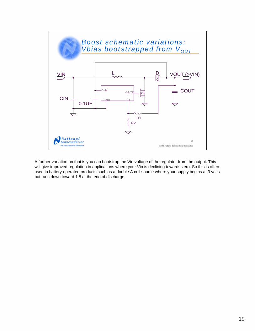
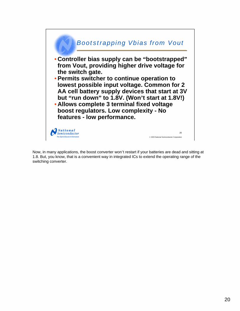
A further variation on that is you can bootstrap the Vin voltage of the regulator from the output. This will give improved regulation in applications where your Vin is declining towards zero. So this is often used in battery-operated products such as a double A cell source where your supply begins at 3 volts but runs down toward 1.8 at the end of discharge.
20
20
© 2003 National Semiconductor Corporation
Bootstrapping Vbias from Vout
• Controller bias supply can be “bootstrapped”from Vout, providing higher drive voltage for the switch gate.
• Permits switcher to continue operation to lowest possible input voltage. Common for 2 AA cell battery supply devices that start at 3V but “run down” to 1.8V. (Won’t start at 1.8V!)
• Allows complete 3 terminal fixed voltage boost regulators. Low complexity - No features - low performance.
Now, in many applications, the boost converter won’t restart if your batteries are dead and sitting at 1.8. But, you know, that is a convenient way in integrated ICs to extend the operating range of the switching converter.
21
21
© 2003 National Semiconductor Corporation
3 Terminal Boost
VOUT (>VIN)D2 1
CIN
L
12VFB
VIN SWITCH COUT
GND
VIN
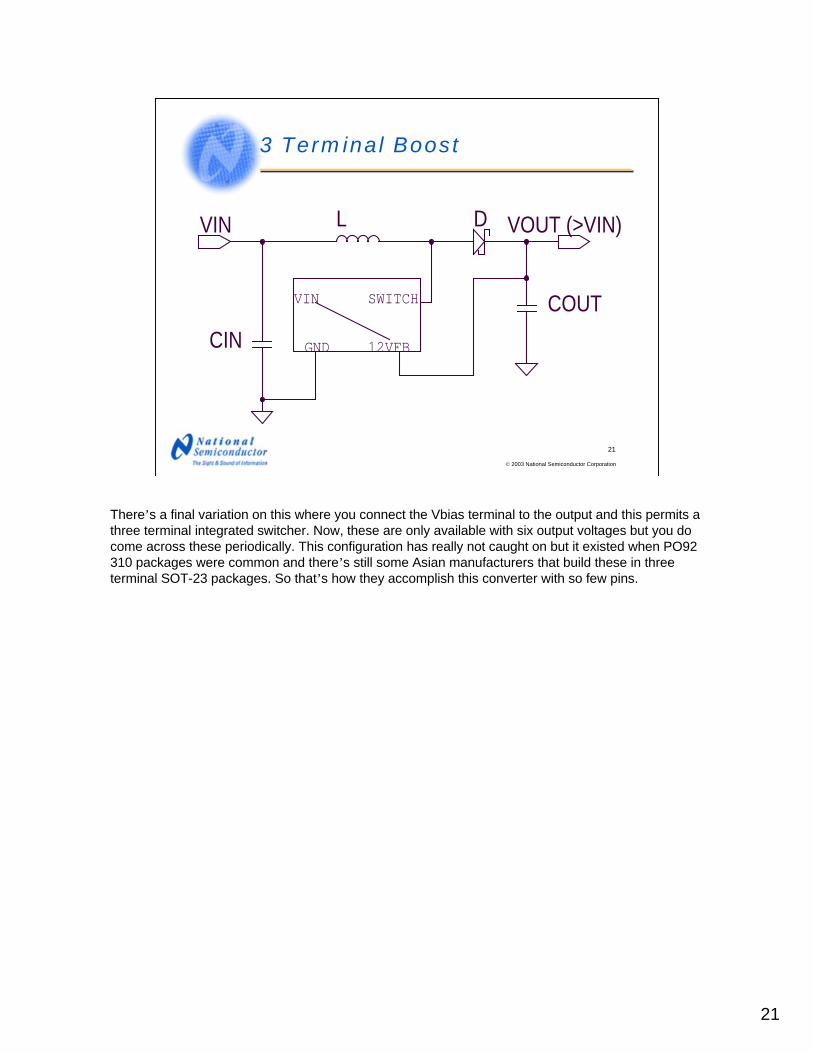
There’s a final variation on this where you connect the Vbias terminal to the output and this permits a three terminal integrated switcher. Now, these are only available with six output voltages but you do come across these periodically. This configuration has really not caught on but it existed when PO92 310 packages were common and there’s still some Asian manufacturers that build these in three terminal SOT-23 packages. So that’s how they accomplish this converter with so few pins.
22
22
© 2003 National Semiconductor Corporation
Common types of boost control sections
• Gated Oscillator– Simple control section– Usually “fixed on-time”– Difficult to filter low freq ripple
• Pulse Frequency mode - PFM– Good light load efficiency– Difficult to filter low freq ripple
• Constant frequency current mode PWM– Most modern parts use this– Requires a current sense method
• SenseFET• Sense resistor – internal or external
• PFM / PWM dual mode – Best of both approaches
Next we’ll cover common types of boost control sections. The simplest type is the gated oscillator. These are rather hysteretic in their performance. They’re low performance overall and it’s difficult to filter the low frequency ripple on their output. These are often fixed-on-time architectures so the duty cycle does not vary while they’re operating. More recently, there’s a type called pulse frequency mode or PFM. These give excellent light load efficiency but at low currents it’s difficult to filter the low frequency ripple out of them.
The most common type of high performance part is the constant frequency current mode PWM. Most modern parts use this. It does require a current sense mechanism for current sensing the peak switch current. This can either be some sort of sense strap or a grounded sense resistor at the bottom of the switching transistor either internally or externally. And then there’s combinations of these two that are combined PFM/PWM dual mode. So those give excellent low load efficiency and good performanceat full load current.
23
23
© 2003 National Semiconductor Corporation
Current mode boost current sensing
1
23
SwitchNodeVIN
R2
FB
COUT
GND SNS
VOUT (>VIN)
CIN
R1
Rsns
VIN
D2 1
GATE
L
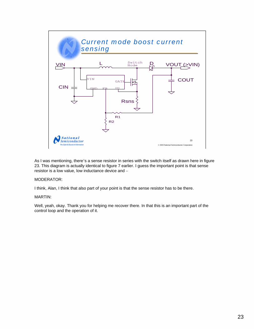
As I was mentioning, there’s a sense resistor in series with the switch itself as drawn here in figure 23. This diagram is actually identical to figure 7 earlier. I guess the important point is that sense resistor is a low value, low inductance device and –
MODERATOR:
I think, Alan, I think that also part of your point is that the sense resistor has to be there.
MARTIN:
Well, yeah, okay. Thank you for helping me recover there. In that this is an important part of the control loop and the operation of it.
24
24
© 2003 National Semiconductor Corporation
Attaching test equipment to a boost converter (1)
• Apply a current probe to the input side of the inductor from Vin. Otherwise, the stray capacitance of the current probe head may cause switching performance problems.
• Added inductance of the current probe is minor effect.
• Measure output voltage ripple directly across terminals of “last” output capacitor. PCB trace inductance will add to reading. Eliminate the scope probe ground lead during measurement.
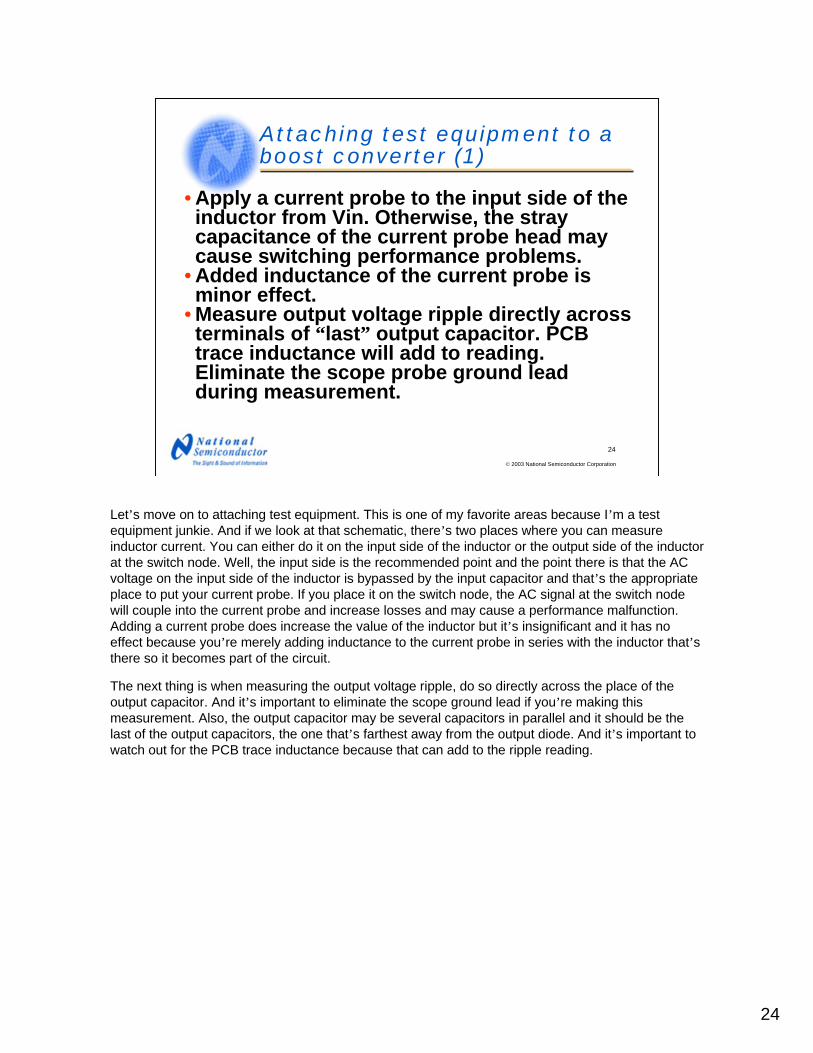
Let’s move on to attaching test equipment. This is one of my favorite areas because I’m a test equipment junkie. And if we look at that schematic, there’s two places where you can measure inductor current. You can either do it on the input side of the inductor or the output side of the inductor at the switch node. Well, the input side is the recommended point and the point there is that the AC voltage on the input side of the inductor is bypassed by the input capacitor and that’s the appropriate place to put your current probe. If you place it on the switch node, the AC signal at the switch node will couple into the current probe and increase losses and may cause a performance malfunction. Adding a current probe does increase the value of the inductor but it’s insignificant and it has no effect because you’re merely adding inductance to the current probe in series with the inductor that’s there so it becomes part of the circuit.
The next thing is when measuring the output voltage ripple, do so directly across the place of the output capacitor. And it’s important to eliminate the scope ground lead if you’re making this measurement. Also, the output capacitor may be several capacitors in parallel and it should be the last of the output capacitors, the one that’s farthest away from the output diode. And it’s important to watch out for the PCB trace inductance because that can add to the ripple reading.
25
25
© 2003 National Semiconductor Corporation
Attaching test equipment to a boost converter (2)
• Feedback input is a sensitive node. Avoid measurement with a multi-meter with unshielded leads. Use a 10X scope probe and scope or attach a series 10K resistor before connecting the multi-meter lead.
• NEVER short the feedback input while the switcher is running. Vout will increase until something breaks.
• NEVER open the feedback loop either.
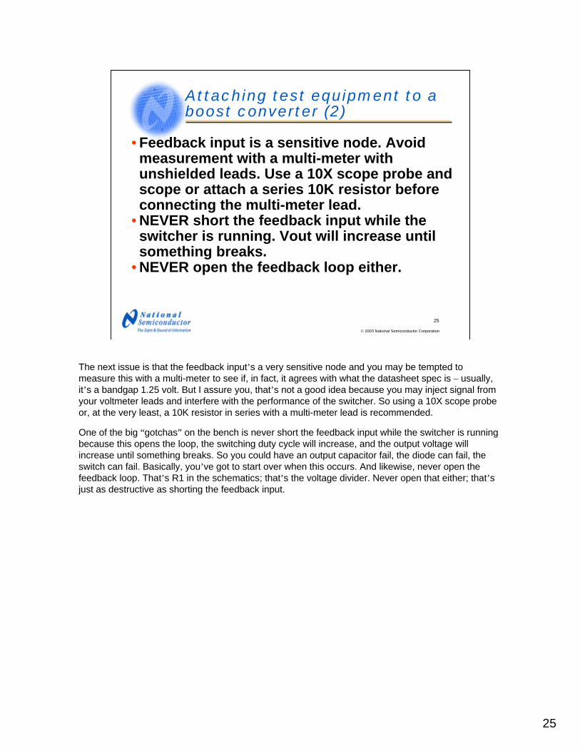
The next issue is that the feedback input’s a very sensitive node and you may be tempted to measure this with a multi-meter to see if, in fact, it agrees with what the datasheet spec is – usually, it’s a bandgap 1.25 volt. But I assure you, that’s not a good idea because you may inject signal from your voltmeter leads and interfere with the performance of the switcher. So using a 10X scope probe or, at the very least, a 10K resistor in series with a multi-meter lead is recommended.
One of the big “gotchas” on the bench is never short the feedback input while the switcher is running because this opens the loop, the switching duty cycle will increase, and the output voltage will increase until something breaks. So you could have an output capacitor fail, the diode can fail, the switch can fail. Basically, you’ve got to start over when this occurs. And likewise, never open the feedback loop. That’s R1 in the schematics; that’s the voltage divider. Never open that either; that’s just as destructive as shorting the feedback input.
26
26
© 2003 National Semiconductor Corporation
Efficiency Measurement
• Connect voltmeter leads directly to bench circuit. (Kelvin connection)
• Then have separate leads for applying power and connecting to load.
Efficiency =VOUT x IOUT
VIN x IIN
D.U.T.
Volts
LoadSource
VOUTVoltsVIN
AmpsAmps
IIN IOUT
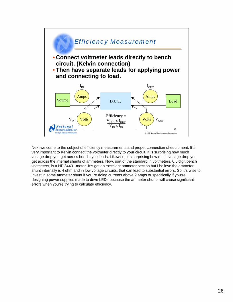
Next we come to the subject of efficiency measurements and proper connection of equipment. It’s very important to Kelvin connect the voltmeter directly to your circuit. It is surprising how much voltage drop you get across bench type leads. Likewise, it’s surprising how much voltage drop you get across the internal shunts of ammeters. Now, sort of the standard in voltmeters, 6.5 digit bench voltmeters, is a HP 34401 meter. It’s got an excellent ammeter section but I believe the ammeter shunt internally is 4 ohm and in low voltage circuits, that can lead to substantial errors. So it’s wise to invest in some ammeter shunt if you’re doing currents above 2 amps or specifically if you’re designing power supplies made to drive LEDs because the ammeter shunts will cause significant errors when you’re trying to calculate efficiency.
27
27
© 2003 National Semiconductor Corporation
Loading a supply under test
• Need a load that is easily varied• Power rating of load must be greater than the supply under
test• Clarostat 240-C Power resistor decade box
– 50W/5A limit on lowest range– Useful to 100’s of volts– Hard to break– Not attractive
• Electronic loads– Kikusui– HP / Agilent– Chroma– Home brew– Recommend using Constant Resistance mode with boost
converters– Constant Current mode will have problems with start-up on
boost converters.– Internal load steppers usually too slow to properly test
transient response
Next comes the subject of applying a load. You need a load that’s easily varied and the power rating of the load must be greater than the supply under test, of course, otherwise you’ll overheat the load. And really one of the best products for a boost converter is an old, old product called a Clarostat 240-C. This is a big power resistor decade box. It’s got a 50 watt limit and it goes from 1 ohm to, I believe, 10 meg ohms in 1 ohm steps. Now, it’s not particularly accurate but that’s really not important. But one of the other features is that it’s useful to hundreds of volts. It’s really hard to break. They’re particularly unattractive and that keeps the resale price down. You can find these on the auction Websites for less than $100 or even less at swap meets.
If you want to be a little more advanced, you could get an electronic load. There’s numerous manufacturers that make electronic loads. But with a boost converter, you’re going to have start-up problems if you use them in constant current mode. So be sure and get an electronic load that has a constant resistance mode so you can evaluate the start-up time of your boost converter. Many of these electronic loads have an internal load stepper so you can look at transient response to the supply. I find that the load steppers are always too slow to really properly test transient response so you’ll have to build something with a mosfet and 555 timer and another load resistor and get it placed very close to your power supply under test if you really want to do a good job of load step transient response.
28
28
© 2003 National Semiconductor Corporation
Frequency Response Analyzer connection
CIN
SwitchNode
COUT
VIN VOUT (>VIN)
12
COMP
SRC
R2
L
C1
D2 1
C2
VIN
R1
GND
R3
FB
1
23
GATE
Rinj100
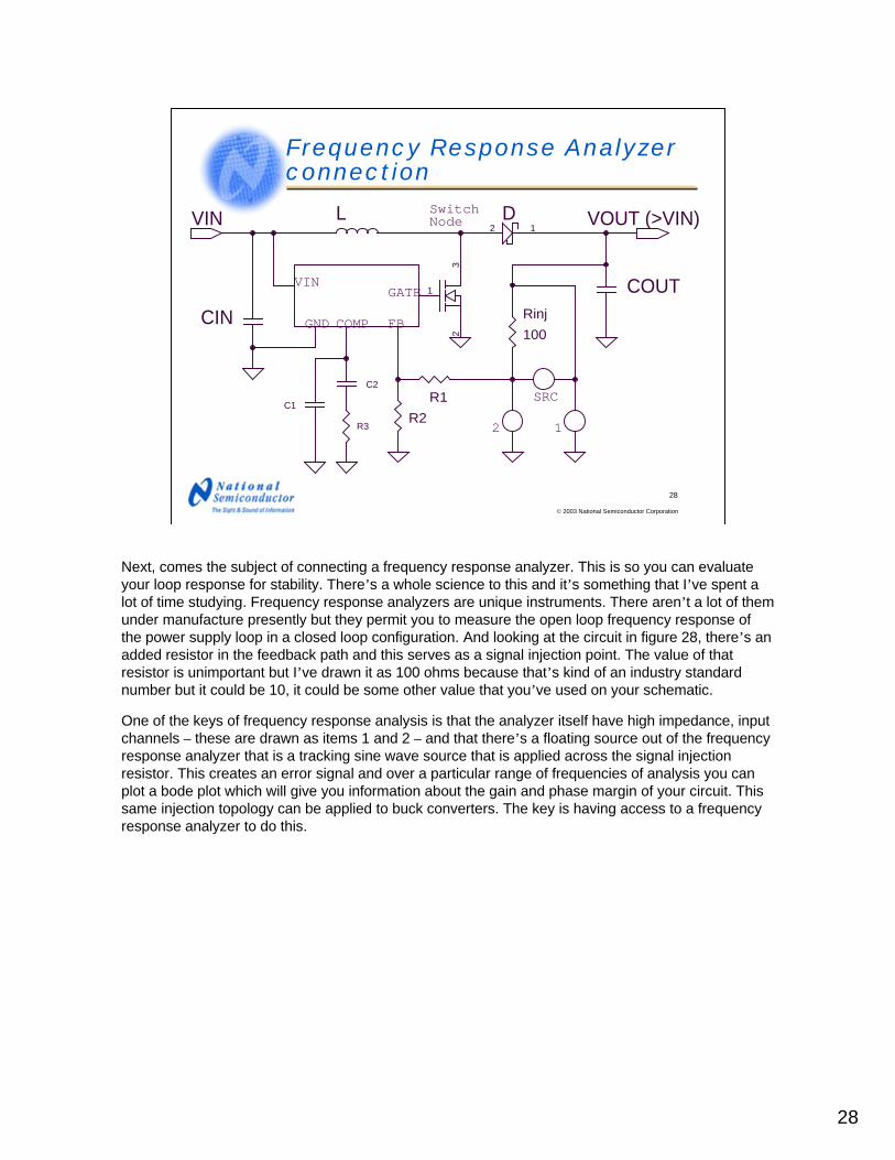
Next, comes the subject of connecting a frequency response analyzer. This is so you can evaluate your loop response for stability. There’s a whole science to this and it’s something that I’ve spent a lot of time studying. Frequency response analyzers are unique instruments. There aren’t a lot of them under manufacture presently but they permit you to measure the open loop frequency response of the power supply loop in a closed loop configuration. And looking at the circuit in figure 28, there’s an added resistor in the feedback path and this serves as a signal injection point. The value of that resistor is unimportant but I’ve drawn it as 100 ohms because that’s kind of an industry standard number but it could be 10, it could be some other value that you’ve used on your schematic.
One of the keys of frequency response analysis is that the analyzer itself have high impedance, input channels – these are drawn as items 1 and 2 – and that there’s a floating source out of the frequency response analyzer that is a tracking sine wave source that is applied across the signal injection resistor. This creates an error signal and over a particular range of frequencies of analysis you can plot a bode plot which will give you information about the gain and phase margin of your circuit. This same injection topology can be applied to buck converters. The key is having access to a frequency response analyzer to do this.

29
29
© 2003 National Semiconductor Corporation
FRA Manufacturers
• Venable Industries - 2.2 MHz max freq– Model 350 HPIB/GPIB/IEEE488 Big
• Japan NF Instruments– Model 3120 - Portable
• Ridley Engineering (AP Instruments)– Model AP200 – 15MHz max– USB and parallel port models - Portable
• HP 4194A or 4195 – discontinued– 10 Hz to 100 MHz Very Big
• Dynamic Signal Analyzers 100kHz max– HP 3562A - HPIB– Stanford Research
A quick review of manufacturers. Venable Industries has been doing this for years. There’s several downsides to their equipment in that it’s particularly large and the frequency response limit is 2.2 MHz. They make two models – well, they make more than that, but the common industry standard model is the model 350. It was actually manufactured for them by a company in Japan called NF Instruments. It’s an HPIB controlled instrument and software available from Venable Industries drives that. One downside is that it’s an older HPIB interface and you may have difficulty supporting that interface on a modern computer. It’s also very large and non-portable. They’ve updated that recently with a model 3120. That’s either a printer interface or a USB so that’s suitable for running with a laptop computer. And it’s nice and it’s compact. It still has the 2.2 MHz frequency limit.
Ridley Engineering is a new company with an offering. The instrument’s actually made by AP Instruments. The model number is an AP200. Very nice thing about this is it’s a 15 MHz max. Now, going to 1 MHz is actually adequate for any of the loop responses you’re going to find on common regulators. But being able to go to 15 MHz permits you to evaluate parasitic of inductors and transformers and input and output caps. So these are very handy for analyzing AC characteristics.
There’s some older HP products that are available, 4194. These are discontinued. They’re still very expensive on the used market but they are out there and maybe there’s one available in your equipment pool. Some of these HP instruments are designed with 50 ohm input so you’ll be required to use fet voltage mode probes on them and you may have some difficulty getting the floating dry voltage to impress across the signal injection resistor.
There’s some other instruments called Dynamic Signal Analyzers which can be applied. This may work but, again, they only go to 100 kHz. But HP 3562, very commonly available on the used market and quite low cost. One difficulty with it is HPIB, it does not have a floppy drive and it’s very difficult to get information out except to an HPIB plotter. There’s newer equipment from Stanford Research that may be applicable also.
30
30
© 2003 National Semiconductor Corporation
Inductor Conduction modes
• Discontinuous conduction mode DCM• Continuous conduction mode CCM
– Observe inductor current with an AC-DC current probe. You need one if you are going to work on switching mode supplies.
• Tektronix & LeCroy produce them• Expensive• Fragile - Don’t drop or exceed ratings• Keep them locked up and hidden• Don’t lend them out
Next, we’re going to talk about inductor conduction mode. Most current mode controllers at full load current are running in continuous conduction mode but at lower load currents they run at discontinuous conduction mode. And the loop response is different for these two modes and that’s something that’s covered very well in literature from Middlebrook and Erickson. Touching again on current probes, if you apply a current probe to the inductor input, you can view these waveforms that are in the next drawings. And current probes themselves are also expensive and if you’re going to work on switching mode supplies, you absolutely need to have access to one. In a voltage domain, you’re rather crippled in terms of seeing what’s going on. Tektronix and LeCroy are both common manufacturers of current probes. The LeCroy ones are specifically made to tie directly to their brand of oscilloscope. The Tektronix ones come in two styles, some that are only compatible with Tektronix scopes and some that are general purpose that have a 50 ohm output cable. All current probes are expensive, they’re very fragile, and I really cannot highlight enough – don’t drop them and don’t be tempted to exceed their ratings because it’s a very expensive mistake. And also keep them locked up and hidden. Don’t lend them out, they tend to walk off.

31
31
© 2003 National Semiconductor Corporation
Discontinuous conduction mode
VIN
VOUT
DCMINDUCTORCURRENT
B
A'
SWITCHNODEVOLTAGE
C'B'
E
BA
DC
Ipk
0A
0V
D'
So looking at our first current here – this is sort of a poor graphic I have to apologize for in terms of the section E. So from point A to B, the switch node is attached to ground. Inductor current is climbing, the switch opens between point C and D, and the inductor current decreases all the way down to zero and this is what signifies discontinuous conduction mode. Now, in point E, this is supposed to represent a sinusoidal ring out around Vin. And a lot of people look at this in the voltage domain and think, “Oh God, there’s something wrong with the power supply. I need to do something to damp out that ringing.” And, in fact, there’s nothing wrong with that ringing with a possible exception if it’s so large that it rings out and goes all the way down to zero volts. There’s some ICs that may malfunction if that’s the case. But generally, that sinusoidal ring out in discontinuous conduction mode is not an issue at all and it’s just something you should be aware of as you adjust the loading of your power supply.
32
32
© 2003 National Semiconductor Corporation
Continuous conduction mode
C
CCMIpk
INDUCTORCURRENT
SWITCHNODEVOLTAGE
0V
VOUT
0A
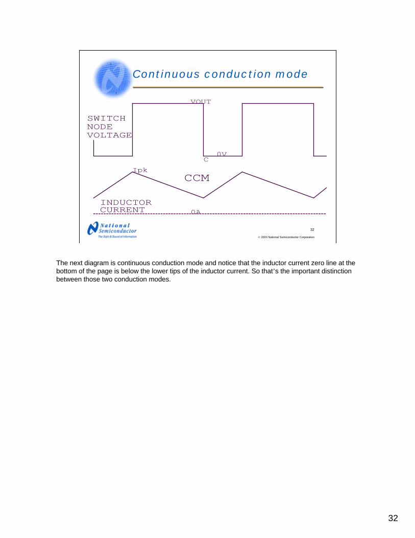
The next diagram is continuous conduction mode and notice that the inductor current zero line at the bottom of the page is below the lower tips of the inductor current. So that’s the important distinction between those two conduction modes.
33
33
© 2003 National Semiconductor Corporation
Capacitor Chemistry Choices
Tantalum • Do not use for Cin if hot plugging input• Derate voltage by 2X • 35V max -> ~20V max in applications• Don’t exceed ripple current rating• Don’t exceed voltage rating• Don’t reverse polarity
• AVX TPS series• Many others
Next, let’s cover capacitor chemistry choices. Tantalum’s used to be very popular because you can get such a high value in a small package. They’ve become very expensive due to tantalum shortages and they do have some limitations that you should be aware of. For example, it’s really not recommended using tantalum as the input capacitor in these designs if you’re going to hot plug from a powered wall adapter. This can exceed the current rating, the surge current rating of the capacitor and cause failure. It’s also recommended, just through experience, to derate the voltage by 2X. So you’ve got a 20 volt capacitor, don’t use it in an application above 10. Or if you’ve got a 5 volt rail, always use a 10 volt cap. Tantalums are limited in the available ratings to about 35 volts so 20 volts is probably the highest application voltage you would use a tantalum in. It’s important not to exceed the ripple current rating with a current probe and a true RMS meter you can see what the actual ripple current is in either the input or the output cap. It’s important never to exceed the voltage rating under transient conditions and don’t ever reverse the polarity. Both of these can lead to failure. There’s many manufacturers; the most common in power supplies is the AVX TPS series – that stands for tantalum power supplies so it’s very easy to remember those when you’re looking for data. There’s many other manufacturers but that’s the one I’m most familiar with.

34
34
© 2003 National Semiconductor Corporation
Capacitor Chemistry Choices
Aluminum electrolytic• Always parallel w/ at least 1uFd of ceramic• Look for low ESR in title and 100kHz data• Voltage ratings from 6.3V up to 450VDC• Derate voltage to ~ 80%• Values from 1 uFd up to many 1000ufd.• Lowest cost• Least reliable if hot environment
SanyoPanasonicMany others
Next are aluminum electrolytics. It’s important in a switching mode power supply that if you’re going to use aluminum electrolytic that you should always parallel with at least 1 uFd of ceramic. And this helps bypass the internal inductance. When selecting aluminum electrolytics and viewing datasheets, always look for a brag phrase in the title where they’re saying that it is low ESR and it’s imperative that there be data at 100 kHz. If there’s only data at 120 Hz then those are really not appropriate for switching mode power supplies. Aluminum electrolytics are available in voltage ratings from 6.3 to 450 volts. It’s probably appropriate to derate them about 80% instead of 2X as with the tantalum. And you can find values from 1 uFd to many thousands of uFds but probably the 10 to 100 uFd range is what you’ll find mostly in switching mode supply. These are the lowest cost but they’re also the least reliable because internally they are wet and they will eventually dry out if used in an extended period of a hot environment. Sanyo and Panasonic are common manufacturers. There’s many, many others.
35
35
© 2003 National Semiconductor Corporation
Capacitor Chemistry Choices
– Ceramic• Use X7R, X5R, X5S, never Z5U or Y5V• Values up to 100UF at 6.3V• Large sizes may crack with PCB flexing• Max voltage about 50V for high C units (they
tolerate voltages much higher than rating)– Taiyo Yuden– Murata– Marcon / United Chemicon– AVX
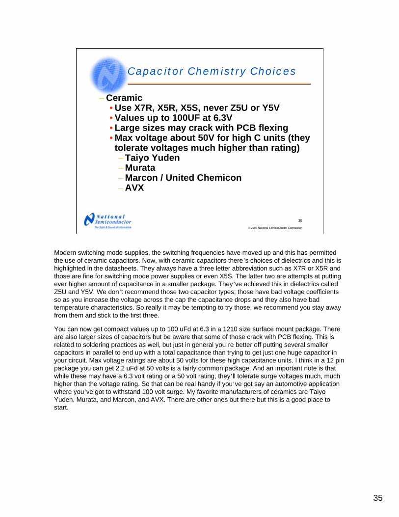
Modern switching mode supplies, the switching frequencies have moved up and this has permitted the use of ceramic capacitors. Now, with ceramic capacitors there’s choices of dielectrics and this is highlighted in the datasheets. They always have a three letter abbreviation such as X7R or X5R and those are fine for switching mode power supplies or even X5S. The latter two are attempts at putting ever higher amount of capacitance in a smaller package. They’ve achieved this in dielectrics called Z5U and Y5V. We don’t recommend those two capacitor types; those have bad voltage coefficients so as you increase the voltage across the cap the capacitance drops and they also have bad temperature characteristics. So really it may be tempting to try those, we recommend you stay away from them and stick to the first three.
You can now get compact values up to 100 uFd at 6.3 in a 1210 size surface mount package. There are also larger sizes of capacitors but be aware that some of those crack with PCB flexing. This is related to soldering practices as well, but just in general you’re better off putting several smaller capacitors in parallel to end up with a total capacitance than trying to get just one huge capacitor in your circuit. Max voltage ratings are about 50 volts for these high capacitance units. I think in a 12 pin package you can get 2.2 uFd at 50 volts is a fairly common package. And an important note is that while these may have a 6.3 volt rating or a 50 volt rating, they’ll tolerate surge voltages much, much higher than the voltage rating. So that can be real handy if you’ve got say an automotive application where you’ve got to withstand 100 volt surge. My favorite manufacturers of ceramics are Taiyo Yuden, Murata, and Marcon, and AVX. There are other ones out there but this is a good place to start.
36
36
© 2003 National Semiconductor Corporation
Capacitor Chemistry Choices
– Poscap (Sanyo)– or SPcap (Panasonic) polymer
• Excellent performance• Low ESR• High ripple current rating• Limited choice of voltage ratings (<10V)• Derate voltage ~80%
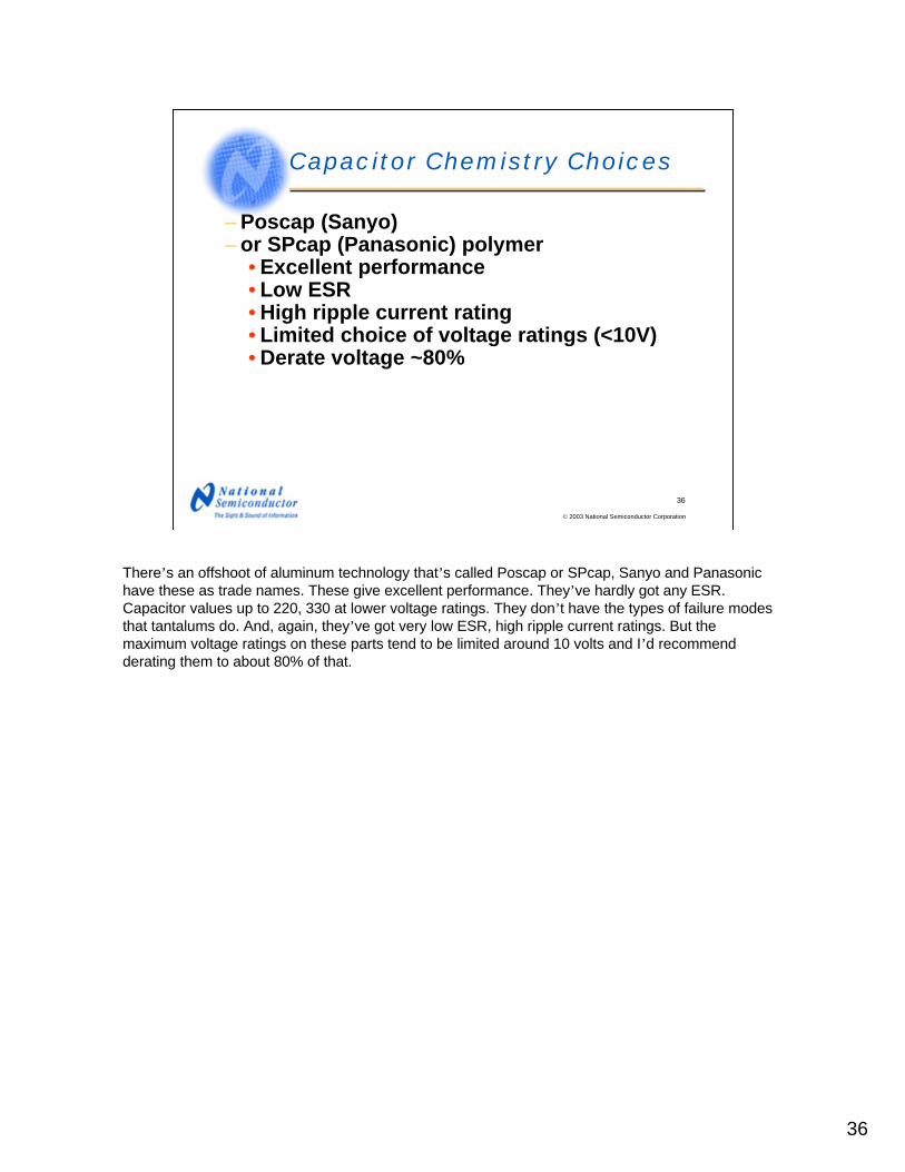
There’s an offshoot of aluminum technology that’s called Poscap or SPcap, Sanyo and Panasonic have these as trade names. These give excellent performance. They’ve hardly got any ESR. Capacitor values up to 220, 330 at lower voltage ratings. They don’t have the types of failure modes that tantalums do. And, again, they’ve got very low ESR, high ripple current ratings. But the maximum voltage ratings on these parts tend to be limited around 10 volts and I’d recommend derating them to about 80% of that.
37
37
© 2003 National Semiconductor Corporation
Capacitor Chemistry Choices
• Sanyo OSCON• Excellent performance• Low ESR• High ripple current rating• Limited choice of voltage ratings (<35V)• Derate voltage ~80%
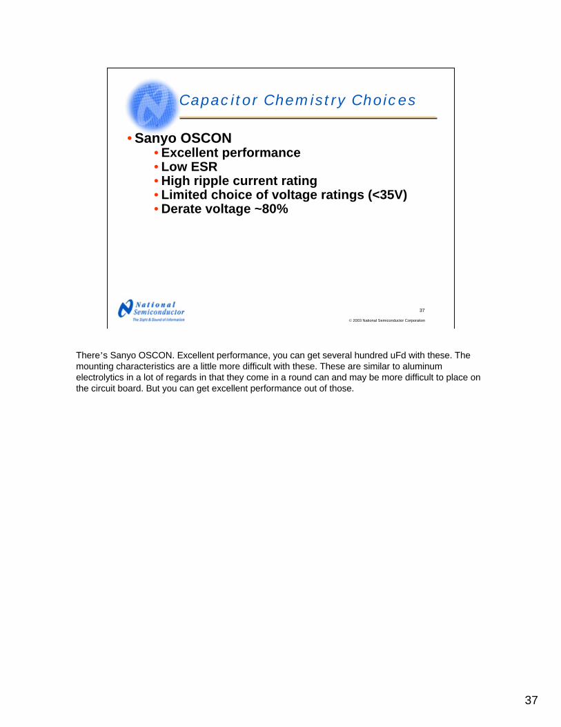
There’s Sanyo OSCON. Excellent performance, you can get several hundred uFd with these. The mounting characteristics are a little more difficult with these. These are similar to aluminum electrolytics in a lot of regards in that they come in a round can and may be more difficult to place on the circuit board. But you can get excellent performance out of those.
38
38
© 2003 National Semiconductor Corporation
Diode selection
• Schottky available up to 100VPIV– Derate ~80%– Diodes Inc – Best selection of packages– Central Semiconductor– On Semiconductor (formerly Motorola)
• Ultra Fast recovery• Small signal silicon 1N4148/1N914
– Low cost / low current• 1N4007 type far too slow
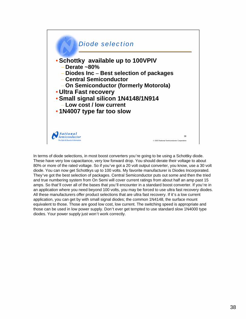
In terms of diode selections, in most boost converters you’re going to be using a Schottky diode. These have very low capacitance, very low forward drop. You should derate their voltage to about 80% or more of the rated voltage. So if you’ve got a 20 volt output converter, you know, use a 30 volt diode. You can now get Schottkys up to 100 volts. My favorite manufacturer is Diodes Incorporated. They’ve got the best selection of packages. Central Semiconductor puts out some and then the tried and true numbering system from On Semi will cover current ratings from about half an amp past 15 amps. So that’ll cover all of the bases that you’ll encounter in a standard boost converter. If you’re in an application where you need beyond 100 volts, you may be forced to use ultra fast recovery diodes. All these manufacturers offer product selections that are ultra fast recovery. If it’s a low current application, you can get by with small signal diodes; the common 1N4148, the surface mount equivalent to those. Those are good low cost, low current. The switching speed is appropriate and those can be used in low power supply. Don’t ever get tempted to use standard slow 1N4000 type diodes. Your power supply just won’t work correctly.
39
39
© 2003 National Semiconductor Corporation
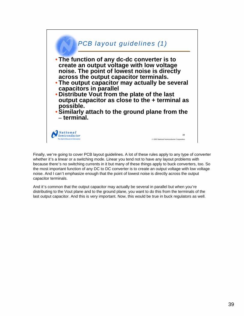
PCB layout guidelines (1)
• The function of any dc-dc converter is to create an output voltage with low voltage noise. The point of lowest noise is directly across the output capacitor terminals.
• The output capacitor may actually be several capacitors in parallel
• Distribute Vout from the plate of the last output capacitor as close to the + terminal as possible.
• Similarly attach to the ground plane from the – terminal.
Finally, we’re going to cover PCB layout guidelines. A lot of these rules apply to any type of converter whether it’s a linear or a switching mode. Linear you tend not to have any layout problems with because there’s no switching currents in it but many of these things apply to buck converters, too. So the most important function of any DC to DC converter is to create an output voltage with low voltage noise. And I can’t emphasize enough that the point of lowest noise is directly across the output capacitor terminals.
And it’s common that the output capacitor may actually be several in parallel but when you’re distributing to the Vout plane and to the ground plane, you want to do this from the terminals of the last output capacitor. And this is very important. Now, this would be true in buck regulators as well.
40
40
© 2003 National Semiconductor Corporation
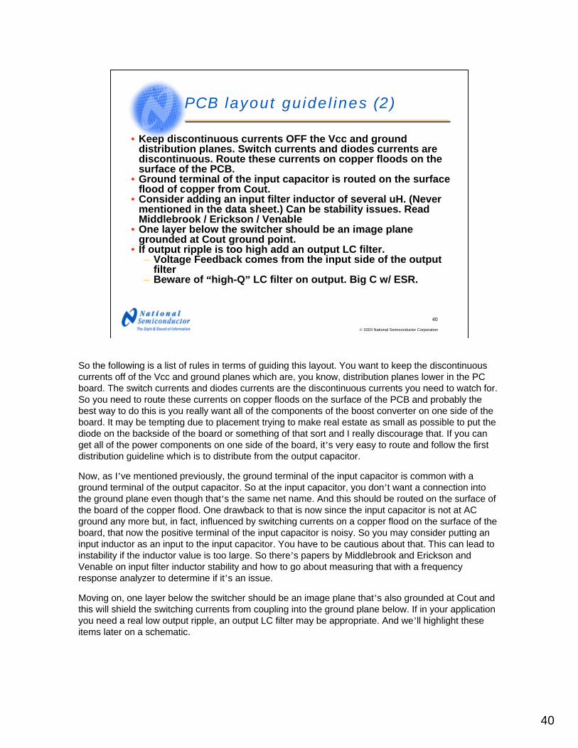
PCB layout guidelines (2)
• Keep discontinuous currents OFF the Vcc and ground distribution planes. Switch currents and diodes currents are discontinuous. Route these currents on copper floods on the surface of the PCB.
• Ground terminal of the input capacitor is routed on the surface flood of copper from Cout.
• Consider adding an input filter inductor of several uH. (Never mentioned in the data sheet.) Can be stability issues. Read Middlebrook / Erickson / Venable
• One layer below the switcher should be an image plane grounded at Cout ground point.
• If output ripple is too high add an output LC filter.– Voltage Feedback comes from the input side of the output
filter– Beware of “high-Q” LC filter on output. Big C w/ ESR.
So the following is a list of rules in terms of guiding this layout. You want to keep the discontinuous currents off of the Vcc and ground planes which are, you know, distribution planes lower in the PC board. The switch currents and diodes currents are the discontinuous currents you need to watch for. So you need to route these currents on copper floods on the surface of the PCB and probably the best way to do this is you really want all of the components of the boost converter on one side of the board. It may be tempting due to placement trying to make real estate as small as possible to put the diode on the backside of the board or something of that sort and I really discourage that. If you can get all of the power components on one side of the board, it’s very easy to route and follow the first distribution guideline which is to distribute from the output capacitor.
Now, as I’ve mentioned previously, the ground terminal of the input capacitor is common with a ground terminal of the output capacitor. So at the input capacitor, you don’t want a connection into the ground plane even though that’s the same net name. And this should be routed on the surface of the board of the copper flood. One drawback to that is now since the input capacitor is not at AC ground any more but, in fact, influenced by switching currents on a copper flood on the surface of the board, that now the positive terminal of the input capacitor is noisy. So you may consider putting an input inductor as an input to the input capacitor. You have to be cautious about that. This can lead to instability if the inductor value is too large. So there’s papers by Middlebrook and Erickson and Venable on input filter inductor stability and how to go about measuring that with a frequency response analyzer to determine if it’s an issue.
Moving on, one layer below the switcher should be an image plane that’s also grounded at Cout and this will shield the switching currents from coupling into the ground plane below. If in your application you need a real low output ripple, an output LC filter may be appropriate. And we’ll highlight these items later on a schematic.
41
41
© 2003 National Semiconductor Corporation
PCB layout guidelines: TO263
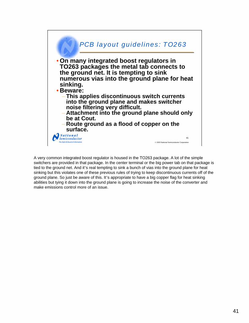
• On many integrated boost regulators in TO263 packages the metal tab connects to the ground net. It is tempting to sink numerous vias into the ground plane for heat sinking.
• Beware: – This applies discontinuous switch currents
into the ground plane and makes switcher noise filtering very difficult.
– Attachment into the ground plane should only be at Cout.
– Route ground as a flood of copper on the surface.
A very common integrated boost regulator is housed in the TO263 package. A lot of the simple switchers are provided in that package. In the center terminal or the big power tab on that package is tied to the ground net. And it’s real tempting to sink a bunch of vias into the ground plane for heat sinking but this violates one of these previous rules of trying to keep discontinuous currents off of the ground plane. So just be aware of this. It’s appropriate to have a big copper flag for heat sinking abilities but tying it down into the ground plane is going to increase the noise of the converter and make emissions control more of an issue.
42
42
© 2003 National Semiconductor Corporation
PCB layout guidelines: on vias
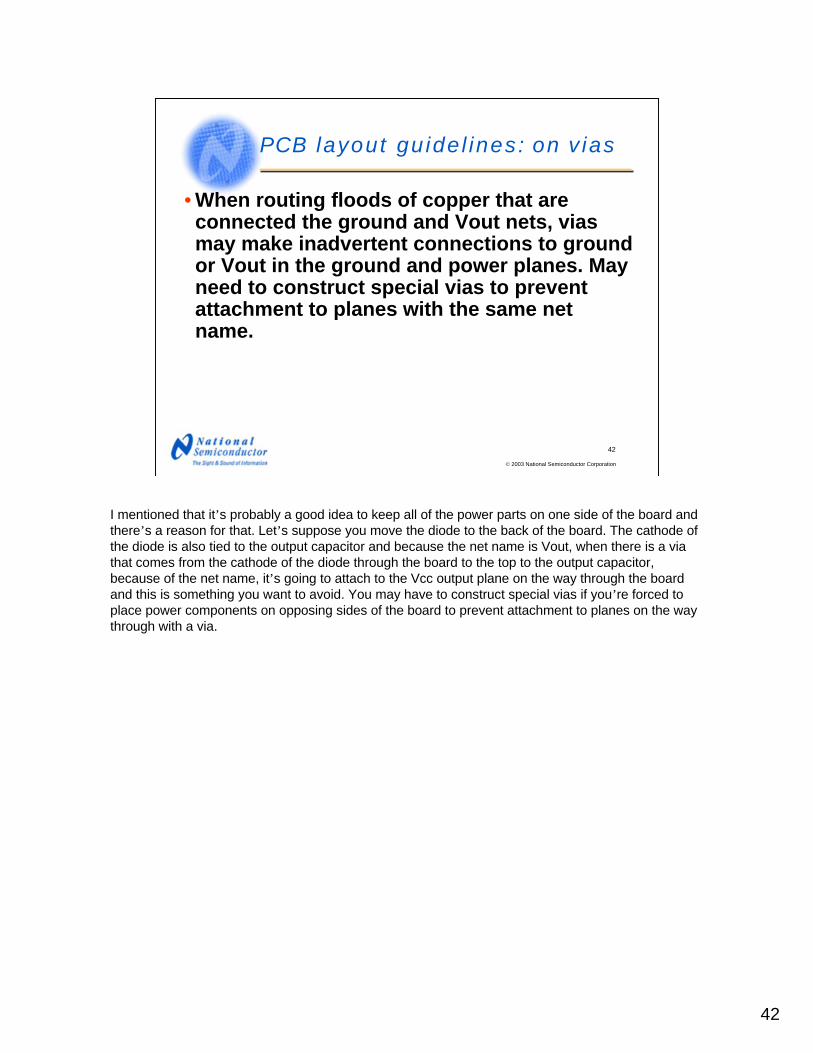
• When routing floods of copper that are connected the ground and Vout nets, viasmay make inadvertent connections to ground or Vout in the ground and power planes. May need to construct special vias to prevent attachment to planes with the same net name.
I mentioned that it’s probably a good idea to keep all of the power parts on one side of the board and there’s a reason for that. Let’s suppose you move the diode to the back of the board. The cathode of the diode is also tied to the output capacitor and because the net name is Vout, when there is a via that comes from the cathode of the diode through the board to the top to the output capacitor, because of the net name, it’s going to attach to the Vcc output plane on the way through the board and this is something you want to avoid. You may have to construct special vias if you’re forced to place power components on opposing sides of the board to prevent attachment to planes on the way through with a via.
43
43
© 2003 National Semiconductor Corporation
PCB layout guidelines, schematic view
R2
FB
SwitchNode
VINVOUT
VIN
1UF+22UF
D2 1
GNDPLANE
1
23
GATE
L
1UFCIN
LoutputLinput
GND
R1
COUT
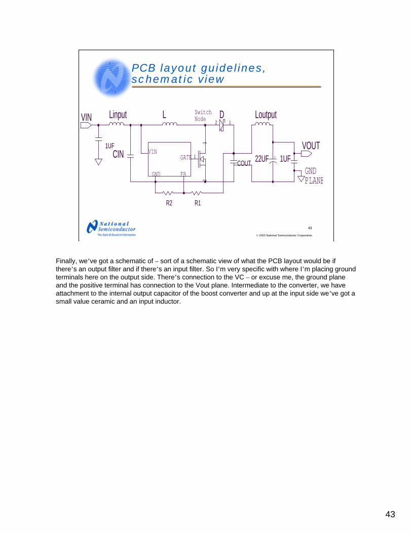
Finally, we’ve got a schematic of – sort of a schematic view of what the PCB layout would be if there’s an output filter and if there’s an input filter. So I’m very specific with where I’m placing ground terminals here on the output side. There’s connection to the VC – or excuse me, the ground plane and the positive terminal has connection to the Vout plane. Intermediate to the converter, we have attachment to the internal output capacitor of the boost converter and up at the input side we’ve got a small value ceramic and an input inductor.

44
44
© 2003 National Semiconductor Corporation
Boost Regulator Design Resources
• Power.national.com online resources
• Power WEBENCH Online Design– www.national.com/appinfo/power/webench
• General-purpose Boost IC datasheets– LM5000 High Voltage Switch Mode Regulator– LM3478 High Efficiency Low-Side N-Channel
Controller for Switching Regulator – LM2577 SIMPLE SWITCHER Step-Up Voltage
Regulator
Following are some design resources available from National, as well as some recommended ICs you might look at in the National product line. And that concludes our presentation and I’ll turn it over to Wanda.
45
45
Thank You
Thank you, Alan, and thank you, everyone, for joining us for the seminar, Boost Converter Design Tips, brought to you by National Semiconductor. This concludes today’s online seminar. When you close your seminar window, a survey form will appear. Please fill out and submit the survey form, your answers to this survey will help us in the development of new products as well as future seminars. Thank you for attending and have a great day!– (END OF PRESENTATION)