bistable circuit
TRANSCRIPT

3.1 Bistable Element Let us look at the inverter. If you provide the inverter input with a 1, the inverter will output a 0. If you do not provide the inverter with an input (that is neither a 0 nor a 1), the inverter will not have a value to output. If you want to construct a memory circuit using the inverter, you would want the inverter to continue to output the 0 even after you remove the 1 input. In order for the inverter to continue to output a 0, you need the inverter to self-provide its own input. In other words, you want the output to feed back the 0 to the input. However, you cannot connect the output of the inverter directly to its input, because you will have a 0 connected to a 1 and so creating a short circuit. The solution is to connect two inverters in series, as shown in Figure 2.1(a). This circuit is called a bistable element, and it is the simplest memory circuit. The bistable element has two symmetrical nodes labeled Q and Q', both of which can be viewed as either an input or an output signal. Since Q and Q' are symmetrical, we can arbitrarily use Q as the state variable, so that the state of the circuit is the value at Q. Let us assume that Q originally has the value 0 when power is first applied to the circuit. Since Q is the input to the bottom inverter, therefore, Q' is a 1. A 1 going to the input of the top inverter will produce a 0 at the output Q, which is what we started off with. Hence, the value at Q will remain at a 0 indefinitely. Similarly, if we power-up the circuit with Q = 1, we will get Q' = 0, and again, we get a stable situation with Q remaining at a 1 indefinitely. Thus, the circuit has two stable states: Q = 0 and Q = 1; hence, the name “bistable.”
Figure 2.1(a) Bistable element circuit.
We say that the bistable element has memory because it can remember its state (i.e., keep the value at Q constant) indefinitely. Unfortunately, we cannot change its state (i.e., cannot change the value at Q). We cannot just input a different value to Q, because it will create a short circuit by connecting a 0 to a 1. For example, let us assume that Q is currently 0. If we want to change the state, we need to set Q to a 1, but in so doing we will be connecting a 1 to a 0, thus creating a short. Another way of looking at this problem is that we can think of both Q and Q' as being the primary outputs, which means that the circuit does not have any external inputs. Therefore, there is no way for us to input a different value.
3.2 S-R Latch In order to change the state for the bistable element, we need to add external inputs to the circuit. The simplest way to add extra inputs is to replace the two inverters with two NAND gates, as shown in (a) of Figure 2.1(b). This circuit is called an SR latch. In addition to the two outputs Q and Q', there are two inputs S' and R' for set and reset, respectively. Just like the bistable element, the SR latch can be in one of two states: a set state when Q = 1, or a reset state when Q = 0. Following the convention, the primes in S and R denote that these inputs are active-low (i.e., a 0 asserts them, and a 1 de-asserts them). To make the SR latch go to the set state, we simply assert the S' input by setting it to 0 (and de-asserting R'). It doesn’t matter what the other NAND gate input is, because 0 NAND anything

gives a 1, hence Q = 1, and the latch is set. If S' remains at 0 so that Q (which is connected to one input of the bottom NAND gate) remains at 1, and if we now de-assert R' (i.e., set R' to a 1) then the output of the bottom NAND gate will be 0, and so, Q' = 0. This situation is shown in (d) of Figure 2.1(b) at time t0. From this current situation, if we now de-assert S' so that S' = R' = 1, the latch will remain in the set state because Q' (the second input to the top NAND gate) is 0, which will keep Q = 1, as shown at time t1. At time t2, we reset the latch by making R' = 0 (and S' = 1). With R' being a 0, Q' will go to a 1. At the top NAND gate, 1 NAND 1 is 0, thus forcing Q to go to 0. If we de-assert R' next so that, again, we have S' = R' = 1, this time the latch will remain in the reset state, as shown at time t3. Notice the two times (at t1 and t3) when both S' and R' are de-asserted (i.e., S' = R' = 1). At t1, Q is at a 1; whereas, at t3, Q is at a 0. Why is this so? What is different between these two times? The difference is in the value of Q immediately before those times. The value of Q right before t1 is 1; whereas, the value of Q right before t3 is 0. When both inputs are de-asserted, the SR latch remembers its previous state. Previous to t1, Q has the value 1, so at t1, Q remains at a 1. Similarly, previous to t3, Q has the value 0, so at t3, Q remains at a 0.
(c) (d)
Figure 2.1(b): SR latch: (a) circuit using NAND gates; (b) truth table; (c) logic symbol; (d) sample trace.
If both S' and R' are asserted (i.e., S' = R' = 0), then both Q and Q' are equal to a 1, as shown at time t4, since 0 NAND anything gives a 1. Note that there is nothing wrong with having Q equal to Q'. It is just because we named these two points Q and Q' that we don’t like them to be equal. However, we could have used another name say, P instead of Q'.

If one of the input signals is de-asserted earlier than the other, the latch will end up in the state forced by the signal that is de-asserted later, as shown at time t5. At t5, R' is de-asserted first, so the latch goes into the set state with Q = 1, and Q' = 0. A problem exists if both S' and R' are de-asserted at exactly the same time, as shown at time t6. Let us assume for a moment that both gates have exactly the same delay and that the two wire connections between the output of one gate to the input of the other gate also have exactly the same delay. Currently, both Q and Q' are at a 1. If we set S' and R' to a 1 at exactly the same time, then both NAND gates will perform a 1 NAND 1 and will both output a 0 at exactly the same time. The two 0’s will be fed back to the two gate inputs at exactly the same time, because the two wire connections have the same delay. This time around, the two NAND gates will perform a 1 NAND 0 and will both produce a 1 again at exactly the same time. This time, two 1’s will be fed back to the inputs, which again will produce a 0 at the outputs, and so on and on. This oscillating behavior, called the critical race, will continue indefinitely until one outpaces the other. If the two gates do not have exactly the same delay then, the situation is similar to de-asserting one input before the other, and so, the latch will go into one state or the other. However, since we do not know which the faster gate is, therefore, we do not know which state the latch will end up in. Thus, the latch’s next state is undefined. Of course, in practice, it is next to impossible to manufacture two gates and make the two connections with precisely the same delay. In addition, both S' and R' need to be de-asserted at exactly the same time. Nevertheless, if this circuit is used in controlling some mission-critical device, we don’t want even this slim chance to happen. In order to avoid this non-deterministic behavior, we must make sure that the two inputs are never de-asserted at the same time. Note that we do want the situation when both of them are de-asserted, as in times t1 and t3, so that the circuit can remember its current content. We want to de-assert one input after de-asserting the other, but just not de-asserting both of them at exactly the same time. In practice, it is very difficult to guarantee that these two signals are never de-asserted at the same time, so we relax the condition slightly by not having both of them asserted together. In other words, if one is asserted, then the other one cannot be asserted. Therefore, if both of them are never asserted simultaneously, then they cannot be de-asserted at the same time. A minor side benefit for not having both of them asserted together is that Q and Q' are never equal to each other. Recall that, from the names that we have given these two nodes, we do want them to be inverses of each other. From the above analysis, we obtain the truth table in (b) of Figure 2.1(b) for the NAND implementation of the SR latch. In the truth table, Q and Qnext actually represent the same point in the circuit. The difference is that Q is the current value at that point, while Qnext is the new value to be updated in the next time period. Another way of looking at it is that Q is the input to a gate, and Qnext is the output from a gate. In other words, the signal Q goes into a gate, propagates through the two gates, and arrives back at Q as the new signal Qnext. The (c) of Figure 2.1(b) shows the logic symbol for the SR latch. The SR latch can also be implemented using NOR gates, as shown in (a) of Figure 2.1(c). The truth table for this implementation is shown in (b) of Figure 2.1(c). From the truth table, we see that the main difference between this implementation and the NAND implementation is that for the NOR implementation, the S and R inputs are active-high, so that setting S to 1 will set the latch, and setting R to 1 will reset the latch. However, just like the NAND implementation, the latch is set when Q = 1, and reset when Q = 0. The latch remembers its previous state when S = R

= 0. When S = R = 1, both Q and Q' are 0. The logic symbol for the SR latch using NOR implementation is shown in (c) of Figure 2.1(d).
Figure 2.1(c): SR latch: (a) circuit using NOR gates; (b) truth table; (c) logic symbol.
3.2.1 S-R Latch with Enable The SR latch is sensitive to its inputs all the time. In other words, Q will always change when either S or R is asserted. It is sometimes useful to be able to disable the inputs so that asserting them will not cause the latch to change state but to keep its current state. Of course, this is achieved by de-asserting both S and R. Hence, what we want is just one enable signal that will de-assert both S and R. The SR latch with enable (also known as a gated SR latch) shown in (a) of Figure 2.1(d) accomplishes this by adding two extra NAND gates to the original NAND gate implementation of the latch. These two new NAND gates are controlled by the enable input, E, which determines whether the latch is enabled or disabled. When E = 1, the circuit behaves like the normal NAND implementation of the SR latch except that the new S and R inputs are active-high rather than active-low. When E = 0, then S' = R' = 1, and the latch will remain in its previous state regardless of the S and R inputs. The truth table and the logic symbol for the SR latch with enable is shown in (b) and (c) of Figure 2.1(d), respectively. A typical operation of the latch is shown in the sample trace in (d) of Figure 2.1(d). Between t0 and t1, E = 0, so changing the S and R inputs do not affect the output, between t1 and t2, E = 1 and the trace is similar to the trace of Figure 2.1(b) except that the input signals are inverted.
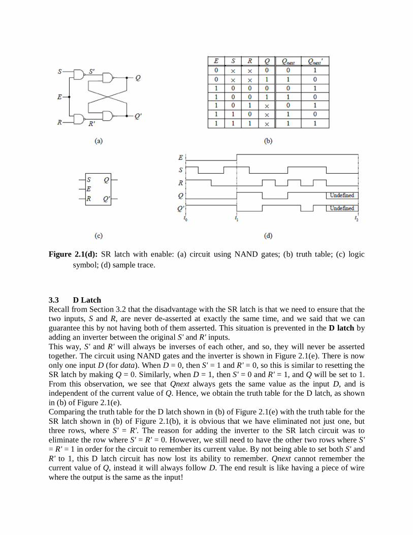
Figure 2.1(d): SR latch with enable: (a) circuit using NAND gates; (b) truth table; (c) logic symbol; (d) sample trace.
3.3 D Latch Recall from Section 3.2 that the disadvantage with the SR latch is that we need to ensure that the two inputs, S and R, are never de-asserted at exactly the same time, and we said that we can guarantee this by not having both of them asserted. This situation is prevented in the D latch by adding an inverter between the original S' and R' inputs. This way, S' and R' will always be inverses of each other, and so, they will never be asserted together. The circuit using NAND gates and the inverter is shown in Figure 2.1(e). There is now only one input D (for data). When D = 0, then S' = 1 and R' = 0, so this is similar to resetting the SR latch by making Q = 0. Similarly, when D = 1, then S' = 0 and R' = 1, and Q will be set to 1. From this observation, we see that Qnext always gets the same value as the input D, and is independent of the current value of Q. Hence, we obtain the truth table for the D latch, as shown in (b) of Figure 2.1(e). Comparing the truth table for the D latch shown in (b) of Figure 2.1(e) with the truth table for the SR latch shown in (b) of Figure 2.1(b), it is obvious that we have eliminated not just one, but three rows, where S' = R'. The reason for adding the inverter to the SR latch circuit was to eliminate the row where S' = R' = 0. However, we still need to have the other two rows where S' = R' = 1 in order for the circuit to remember its current value. By not being able to set both S' and R' to 1, this D latch circuit has now lost its ability to remember. Qnext cannot remember the current value of Q, instead it will always follow D. The end result is like having a piece of wire where the output is the same as the input!

Figure 2.1(e): D latch: (a) circuit using NAND gates; (b) truth table; (c) logic symbol.
3.3.1 D Latch with Enable In order to make the D latch remember the current value, we need to connect Q (the current state value) back to the input D, thus creating another feedback loop. Furthermore, we need to be able to select whether to loop Q back to D or input a new value for D. Otherwise, like the bistable element, we will not be able to change the state of the circuit. One way to achieve this is to use a 2-input multiplexer to select whether to feedback the current value of Q or pass an external input back to D. The circuit for the D latch with enable (also known as a gated D latch) is shown in (a) of Figure 2.1(f). The external input becomes the new D input, the output of the multiplexer is connected to the original D input, and the select line of the multiplexer is the enable signal E. When the enable signal E is asserted (E = 1), the external D input passes through the multiplexer, and so Qnext (i.e., the output Q) follows the D input. On the other hand, when E is de-asserted (E = 0), the current value of Q loops back as the input to the circuit, and so Qnext retains its last value independent of the D input. When the latch is enabled, the latch is said to be open, and the path from the input D to the output Q is transparent. In other words, Q follows D. Because of this characteristic, the D latch with enable circuit is often referred to as a transparent latch. When the latch is disabled, it is closed, and the latch remembers its current state. The truth table and the logic symbol for the D latch with enable are shown in (b) and (c) of Figure 2.1(f). A sample trace for the operation of the D latch with enable is shown in (d) of Figure 2.1(f). Between t0 and t1, the latch is enabled with E = 1, so the output Q follows the input D. Between t1 and t2, the latch is disabled, so Q remains stable even when D changes. An alternative way to construct the D latch with enable circuit is shown in Figure 2.1(g). Instead of using the 2-input multiplexer, as shown in (a) of Figure 2.1(f), we start with the SR latch with enable circuit of (a) of Figure 2.1(f), and connect the S and R inputs together with an inverter. The functional operations of these two circuits are identical.

Figure 2.1(f): D latch with enable: (a) circuit; (b) truth table; (c) logic symbol; (d) sample trace.
Figure 2.1(g): D latch with enable circuit using four NAND gates.
3.4 Analyzing Sequential Circuits
Many logic circuits contain flip-flops, one-shots, and logic gates that are connected to perform a specific operation. Very often, a master clock signal is used to cause the logic levels in the circuit to go through a particular sequence of states. We can generally analyze these sequential circuits by following this step-by-step procedure.
1. Examine the circuit diagram and look for circuit structures such as counters or shift registers that you are familiar with. This can help to simplify the analysis.
2. Determine the logic levels that are present at the inputs of each flip-flop prior to the occurrence of the first clock pulse.

3. Use these levels to determine how each flip-flop output will change in response to the first clock pulse.
4. Repeat steps 2 and 3 for each successive clock pulse.
4.0 Conclusion
The other major aspect of a digital system is the analysis and design of sequential digital circuits. However, sequential circuit design depends, greatly, on the combinational circuit design. The logic circuits whose outputs at any instant of time depend only on the input signals present at that time are known as combinational circuits. On the other hand, the logic circuits whose outputs at any instant of time depend on the present inputs as well as on the past outputs are called sequential circuits. In sequential circuits, the output signals are fed back to the input side. 5.0 Summary
In this unit, you learnt that: Latches and Flip-flops are the building blocks of sequential circuits. Bistable Elements SR Latch D Latch is a circuit that contains a NAND gate latch and two steering NAND gates.
6.0 Tutor Marked Assignment 1) Draw the SR latch with enable but using NOR gates to implement the SR latch. Derive
the truth table for this circuit.
2) Draw the D latch using NOR gates 7.0 Further Reading and Other Resources
1. Ronald J. Tocci (1988). “Digital Systems: Priciples and Applications”, 4th Edition Prentice-Hall International edition.
2. http://en.wikipedia.org/wiki/Logic_gate 3. http://www.discovercircuits.com/D/digital.htm 4. http://www.encyclopedia.com/doc/1G1-168332407.html 5. http://www.logiccircuit.org/

MODULE 2 - Latches and Flip-Flops
UNIT 2: Flip Flops
Contents Pages
1.0 Introduction ……………………………………………………………………. 69
2.0 Objectives ……………………………………………………………………. 69
3.0 Flip-Flops ...………………………..…………………………………………… 69 3.1 S-R (Set-Reset) Flip-flop …. …………………………………………………… 70 3.2 S-R Flip-flop Based on NOR Gates …………………………………………….. 70
3.3 S'-R' Flip-flop Based on NAND Gates………………………………………….. 72
4.0 Conclusion ………………………………………………………………………. 74
5.0 Summary ………………………………………………………………………… 74
6.0 Tutor Marked Assignment…………………….………………………………… 74
7.0 Further Reading and Other Resources …………………………………………… 74

1.0 Introduction There are basically four main types of flip-flops: D, S-R, J-K, and T. The major differences in these flip-flop types are in the number of inputs they have and how they change states. Like the D flip-flop, each type can also have different variations, such as active-high or low inputs, whether they change state at the rising or falling edge of the clock signal, and whether they have any asynchronous inputs. Any given sequential circuit can be built using any of these types of flip-flops or combinations of them. However, selecting one type of flip-flop over another type to use in a particular circuit can affect the overall size of the circuit. Today, sequential circuits are designed primarily with D flip-flops only because of their simple operation. The action of clearing a Flip-Flop or a latch is also called resetting, and both terms are used interchangeably in the digital field. In fact, a CLEAR input can also be called RESET input, and a SET-CLEAR latch can be called a SET-RESET latch, which will be used as S-R throughout our discussions.
2.0 Objective Upon completion of this unit, you will be able to:
Identify the types of flip-flops Discuss the various types of S-R Flip-Flop
3.0 Flip-Flops The most important memory element is the flip-flop, which is made up of an assembly of logic gates. Even though a logic gate by itself has no storage capability, several can be connected together in ways that permit information to be stored. Figure is the general type of symbol used for a flip-flop. It shows two outputs, labeled Q and Q, that are the inverse of each other. Actually, any letter can be used, but Q is the one most often used. The Q output is called the normal flip-flop output, and Q is the inverted flip-flop output. Whenever we refer to the state of a flip-flop, we are referring to the state of its normal (Q) output; it is understood that its inverted output (Q) is in the opposite state. For example, if we say that a flip-flop is in the HIGH (1) state, we mean that Q = 1; if we say that a flip-flop is in the LOW (0) state, we mean that Q = 0. Of course, the Q state will always be the inverse of Q. A flip-flop, then, has the two allowed operating states indicated in (b) of Figure 2.2(a). Note the different ways that are used to refer to these two states. As the symbol in (a) of Figure 2.2(a) implies, a flip-flop can have one or more inputs. These inputs are used to cause the flip-flop to switch back and forth (“flip-flop”) between its possible output states. As we shall see, a Flip-Flop input only has to be pulsed momentarily to cause a change in the Flip-Flop output state, and the output will remain in that new state even after the input pulse is over. This is the Flip-Flop’s memory characteristics.

Figure 2.2(a): General flip-flop symbol and definition of two possible output states There are different types of flip-flops depending on how their inputs and clock pulses cause transition between two states. The most basic FF circuit can be constructed from either two NAND gates or two NOR gates. We will discuss the different types of flip-flops in this unit and the next unit. 3.1 S-R (Set-Reset) Flip-flop An S-R flip-flop has two inputs named Set (S) and Reset (R), and two outputs Q and Q'. The outputs are complement of each other, i.e., if one of the outputs is 0 then the other should be 1. This can be implemented using NAND or NOR gates. The block diagram of an S-R flip-flop is shown in Figure 2.2(b).
Figure 2.2(b): Block diagram for S-R flip-flop.
3.2 S-R Flip-flop Based on NOR Gates An S-R flip-flop can be constructed with NOR gates at ease by connecting the NOR gates back to back as shown in Figure 2.2(c). The cross-coupled connections from the output of gate 1 to the input of gate 2 constitute a feedback path. This circuit is not clocked and is classified as an asynchronous sequential circuit. The truth table for the S-R flip-flop based on a NOR gate is shown in Table 2.2 (a).
: Q
FF
Q
Inputs
Output States Normal Output
Inverted output
Q = 1, Q= 0:
Q = 0, Q= 1:
called HIGH or 1 state; also called SET state
called LOW or 0 state; also called CLEAR or RESET state
(a) (b)

Figure 2.2(c): S-R flip-flop based on a NOR gate
To analyze the circuit shown in Figure 2.2(c), we have to consider the fact that the output of a NOR gate is 0 if any of the inputs are 1, irrespective of the other input. The output is 1 only if all of the inputs are 0. The outputs for all the possible conditions as shown in Table 2.2 (a) are described as follows. Table 2.2(a): Output of S-R flip-flop based on a NOR gate
Case 1. For S = 0 and R = 0, the flip-flop remains in its present state (Qn). It means that the next state of the flip-flop does not change, i.e., Qn+1 = 0 if Qn = 0 and vice versa. First let us assume that Qn = 1 and Q'n = 0. Thus the inputs of NOR gate 2 are 1 and 0, and therefore its output Q'n+1 = 0. This output Q'n+1 = 0 is fed back as the input of NOR gate 1, thereby producing a 1 at the output, as both of the inputs of NOR gate 1 are 0 and 0; so Qn+1 = 1 as originally assumed. Now let us assume the opposite case, i.e., Qn = 0 and Q'n = 1. Thus the inputs of NOR gate 1 are 1 and 0, and therefore its output Qn+1 = 0. This output Qn+1 =0 is fed back as the input of NOR gate 2, thereby producing a 1 at the output, as both of the inputs of NOR gate 2 are 0 and 0; so Q'n+1 = 1 as originally assumed. Thus we find that the condition S = 0 and R = 0 do not affect the outputs of the flip-flop, which means this is the memory condition of the S-R flip-flop. Case 2. The second input condition is S = 0 and R = 1. The 1 at R input forces the output of NOR gate 1 to be 0 (i.e., Qn+1 = 0). Hence both the inputs of NOR gate 2 are 0 and 0 and so its output Q'n+1 = 1. Thus the condition S = 0 and R = 1 will always reset the flip-flop to 0. Now if the R returns to 0 with S = 0, the flip-flop will remain in the same state. Case 3. The third input condition is S = 1 and R = 0. The 1 at S input forces the output of NOR gate 2 to be 0 (i.e., Q'n+1 = 0). Hence both the inputs of NOR gate 1 are 0 and 0 and so its output Qn+1 = 1. Thus the condition S = 1 and R = 0 will always set the flip-flop to 1. Now if the S returns to 0 with R = 0, the flip-flop will remain in the same state. Case 4. The fourth input condition is S = 1 and R = 1. The 1 at R input and 1 at S input forces the output of both NOR gate 1 and NOR gate 2 to be 0. Hence both the outputs of NOR gate 1

and NOR gate 2 are 0 and 0; i.e., Qn+1 = 0 and Q'n+1 = 0. Hence this condition S = 1 and R = 1 violates the fact that the outputs of a flip-flop will always be the complement of each other. Since the condition violates the basic definition of flip-flop, it is called the undefined condition. Generally this condition must be avoided by making sure that 1s are not applied simultaneously to both of the inputs. Case 5. If case 4 arises at all, then S and R both return to 0 and 0 simultaneously, and then any one of the NOR gates acts faster than the other and assumes the state. For example, if NOR gate 1 is faster than NOR gate 2, then Qn+1 will become 1 and this will make Q'n+1 = 0. Similarly, if NOR gate 2 is faster than NOR gate 1, then Q'n+1 will become 1 and this will make Qn+1 = 0. Hence, this condition is determined by the flip-flop itself. Since this condition cannot be controlled and predicted it is called the indeterminate condition. 3.3 S'-R' Flip-flop Based on NAND Gates An S'-R' flip-flop can be constructed with NAND gates by connecting the NAND gates back to back as shown in Figure 2.2(d). The operation of the S'-R' flip-flop can be analyzed in a similar manner as that employed for the NOR-based S-R flip-flop. This circuit is also not clocked and is classified as an asynchronous sequential circuit. The truth table for the S'-R' flip-flop based on a NAND gate is shown in Table 2.2(b)
Figure 2.2(d): NAND-based S'-R' flip-flop.
To analyze the circuit shown in Figure 2.2(c), we have to remember that a LOW at any input of a NAND gate forces the output to be HIGH, irrespective of the other input. The output of a NAND gate is 0 only if all of the inputs of the NAND gate are 1. The outputs for all the possible conditions as shown in Table 2.2(b) are described below.
Table 2.2(b): Output of S-R flip-flop based on a NAND gate

Case 1. For S' = 1 and R' = 1, the flip-flop remains in its present state (Qn). It means that the next state of the flip-flop does not change, i.e., Qn+1 = 0 if Qn = 0 and vice versa. First let us assume that Qn =1 and Q'n = 0. Thus the inputs of NAND gate 1 are 1 and 0, and therefore its output Qn+1 = 1. This output Qn+1 = 1 is fed back as the input of NAND gate 2, thereby producing a 0 at the output, as both of the inputs of NAND gate 2 are 1 and 1; so Q'n+1 = 0 as originally assumed.
Now let us assume the opposite case, i.e., Qn = 0 and Q'n = 1. Thus the inputs of NAND gate 2 are 1 and 0, and therefore its output Q'n+1 = 1. This output Q'n+1 = 1 is fed back as the input of NAND gate 1, thereby producing a 0 at the output, as both of the inputs of NAND gate 1 are 1 and 1; so Qn+1 = 0 as originally assumed. Thus we find that the condition S' = 1 and R' = 1 do not affect the outputs of the flip-flop, which means this is the memory condition of the S'-R' flip-flop. Case 2. The second input condition is S' = 1 and R' = 0. The 0 at R' input forces the output of NAND gate 2 to be 1 (i.e., Q'n+1 = 1). Hence both the inputs of NAND gate 1 are 1 and 1 and so its output Qn+1 = 0. Thus the condition S' = 1 and R' = 0 will always reset the flip-flop to 0. Now if the R' returns to 1 with S' = 1, the flip-flop will remain in the same state. Case 3. The third input condition is S' = 0 and R' = 1. The 0 at S' input forces the output of NAND gate 1 to be 1 (i.e., Qn+1 = 1). Hence both the inputs of NAND gate 2 are 1 and 1 and so its output Q'n+1 = 0. Thus the condition S' = 0 and R' = 1 will always set the flip-flop to 1. Now if the S' returns to 1 with R' = 1, the flip-flop will remain in the same state. Case 4. The fourth input condition is S' = 0 and R' = 0. The 0 at R' input and 0 at S' input forces the output of both NAND gate 1 and NAND gate 2 to be 1. Hence both the outputs of NAND gate 1 and NAND gate 2 are 1 and 1; i.e., Qn+1 = 1 and Q'n+1 = 1. Hence this condition S' = 0 and R' = 0 violates the fact that the outputs of a flip-flop will always be the complement of each other. Since the condition violates the basic definition of a flip-flop, it is called the undefined condition. Generally, this condition must be avoided by making sure that 0s are not applied simultaneously to both of the inputs. Case 5. If case 4 arises at all, then S' and R' both return to 1 and 1 simultaneously, and then any one of the NAND gates acts faster than the other and assumes the state. For example, if NAND gate 1 is faster than NAND gate 2, then Qn+1 will become 1 and this will make Q'n+1 = 0. Similarly, if NAND gate 2 is faster than NAND gate 1, then Q'n+1 will become 1 and this will make Qn+1 = 0. Hence, this condition is determined by the flip-flop itself. Since this condition cannot be controlled and predicted it is called the indeterminate condition.

Figure 2.2(e): An S-R flip-flop using NAND gates
Thus, comparing the NOR flip-flop and the NAND flip-flop, we find that they basically operate in just the complement fashion of each other. Hence, to convert a NAND-based S'-R' flip-flop into a NOR-based S-R flip-flop, we have to place an inverter at each input of the flip-flop. The resulting circuit is shown in Figure 2.2(e), which behaves in the same manner as an S-R flip-flop.
4.0 Conclusion
The basic 1-bit digital memory circuit is known as a flip-flop. It can have only two states, either the 1 state or the 0 state. A flip-flop is also known as a bistable multivibrator. Flip-flops can be obtained by using NAND or NOR gates 5.0 Summary
In this unit, you learnt about: Types of Flip-flops including:
o S-R Flip-flop Based on NOR Gates o S'-R' Flip-flop Based on NAND Gates
6.0 Tutor Marked Assignment
1) What is the normal resting state of the S-R inputs? What is the active state of each input? 2) Derive the truth table for the SR flip-flop with enable. 3) Draw the logic diagram for the SR flip-flop. Use NOR gates. 4) Draw the logic diagram for the SR flip-flop. Use AND gates.
7.0 Further Reading and Other Resources
1. Ronald J. Tocci (1988). “Digital Systems: Priciples and Applications”, 4th Edition Prentice-Hall International edition.
2. http://en.wikipedia.org/wiki/Logic_gate 3. http://www.discovercircuits.com/D/digital.htm 4. http://www.encyclopedia.com/doc/1G1-168332407.html

5. http://www.logiccircuit.org/
MODULE 2 - Latches and Flip-Flops
UNIT 3: Clocked S-R Flip-Flop
Contents Pages
1.0 Introduction …………………………………………………………………… 76
2.0 Objectives …………………………………………………………………… 76
3.0 Clocked Signals and Clocked Flip-Flops……..………………………………. 76 3.1 Clocked S-R flip-flop……………. …………………………………………… 77
3.1.1 Preset and Clear …………………………………………………… 79 3.2 D Flip-Flop……..………………………………………………………………. 80
3.3 D Flip-Flop with Enable…………………………………………………………82
4.0 Conclusion ……………………………………………………………………… 83
5.0 Summary ……………………………………………………………………….. 83
6.0 Tutor Marked Assignment…………………….………………………………… 83
7.0 Further Reading and Other Resources ………………………………………….. 84

1.0 Introduction
Generally, synchronous circuits change their states only when clock pulses are present. The operation of the basic flip-flop can be modified by including an additional input to control the behavior of the circuit. 2.0 Objectives
Understand the Clocked S-R flip-flop Understand D Flip-Flop Understand the initial state of circuit with preset and clear input
3.0 Clocked Signals and Clocked Flip-Flops Digital systems can operate either asynchronously or synchronously. In asynchronous systems, the outputs of logic circuits can change state any time one or more of the inputs change. As asynchronous system is difficult to design and troubleshoot. In synchronous systems, the exact times at which any output can change states is determined by a signal commonly called the clock. The clock signal is generally a rectangular pulse train or squarewave. The clock signal is distributed to all parts of the system, and most (if not all) of the system outputs can change state only when the clock makes a transition. When the clock changes from a 0 to a 1, this is called the positive-going transition (PGT); when the clock goes from 1 to 0, this is the negative-going transition (NGT). Most digital systems are principally synchronous (although there are always some asynchronous parts), since synchronous circuits are easier to design and troubleshoot. They are easier to troubleshoot because the circuit outputs can change only at specific instants of time. In other words, almost everything is synchronized to the clock-signal transitions. The synchronizing action of the clock signals is accomplished through the use of clocked flip-flops that are designed to change states on one or the other of the clock’s transitions. There are types of clocked Flip-flops that are used in a wide range of applications. There are some principal ideas that are common to all of them. 1. Clocked Flip-Flops have a clock input that is typically labeled CLK, CK or CP. We will use CLK. In most clocked Flip-Flops, the CLK input is edge-triggered, which means that it is activated by a signal transition.

2. Clocked Flip-Flops also have one or more control inputs that can have various names, depending on their operation. The control inputs will have no effect on Q until the active clock transition occurs. In other words, their effect is synchronized with the signal applied to CLK. For this reason they are called synchronous control inputs. 3. In summary, we can say that the control inputs get the Flip-Flop outputs ready to change, while the active transition at the CLK input actually triggers the change. 3.1 Clocked S-R flip-flop The circuit shown in Figure 2.3(a) consists of two AND gates. The clock input is connected to both of the AND gates, resulting in LOW outputs when the clock input is LOW. In this situation the changes in S and R inputs will not affect the state (Q) of the flip-flop.
Figure 2.3(a): Block diagram of a clocked S-R flip-flop.
On the other hand, if the clock input is HIGH, the changes in S and R will be passed over by the AND gates and they will cause changes in the output (Q) of the flip-flop. This way, any information, either 1 or 0, can be stored in the flip-flop by applying a HIGH clock input and be retained for any desired period of time by applying a LOW at the clock input. This type of flip-flop is called a clocked S-R flip-flop. Such a clocked S-R flip-flop made up of two AND gates and two NOR gates is shown in Figure 2.3(b)
Figure 2.3(b): A clocked NOR-based S-R flip-flop.

Now the same S-R flip-flop can be constructed using the basic NAND latch and two other NAND gates as shown in Figure 2.3(c). The S and R inputs control the states of the flip-flop in the same way as described earlier for the unclocked S-R flip-flop. However, the flip-flop only responds when the clock signal occurs. The clock pulse input acts as an enable signal for the other two inputs. As long as the clock input remains 0 the outputs of NAND gates 1 and 2 stay at logic 1. This 1 level at the inputs of the basic NAND-based S-R flip flop retains the present state.
Figure 2.3(c): A clocked NAND-based S-R flip-flop The logic symbol of the S-R flip-flop is shown in Figure 2.3(d). It has three inputs: S, R, and CLK. The CLK input is marked with a small triangle. The triangle is a symbol that denotes the fact that the circuit responds to an edge or transition at CLK input. Assuming that the inputs do not change during the presence of the clock pulse, we can express the working of the S-R flip-flop in the form of the truth table in Table 2.3(a). Here, Sn and Rn denote the inputs and Qn the output during the bit time n. Qn+1 denotes the output after the pulse passes, i.e., in the bit time n + 1.
Figure 2.3(d): The logic symbol of the S-R flip-flop
Table 2.3(a): Output of the S-R flip-flop.
Case 1. If Sn = Rn = 0, and the clock pulse is not applied, the output of the flip-flop remains in the present state. Even if Sn = Rn = 0, and the clock pulse is applied, the output at the end of the

clock pulse is the same as the output before the clock pulse, i.e., Qn+1 = Qn. The first row of the table indicates that situation.
Case 2. For Sn = 0 and Rn = 1, if the clock pulse is applied (i.e., CLK = 1), the output of NAND gate 1 becomes 1; whereas the output of NAND gate 2 will be 0. Now a 0 at the input of NAND gate 4 forces the output to be 1, i.e., Q' = 1. This 1 goes to the input of NAND gate 3 to make both the inputs of NAND gate 3 as 1, which forces the output of NAND gate 3 to be 0, i.e., Q =0. Case 3. For Sn = 1 and Rn = 0, if the clock pulse is applied (i.e., CLK = 1), the output of NAND gate 2 becomes 1; whereas the output of NAND gate 1 will be 0. Now a 0 at the input of NAND gate 3 forces the output to be 1, i.e., Q = 1. This 1 goes to the input of NAND gate 4 to make both the inputs of NAND gate 4 as 1, which forces the output of NAND gate 4 to be 0, i.e., Q'=0. Case 4. For Sn = 1 and Rn = 1, if the clock pulse is applied (i.e., CLK = 1), the outputs of both NAND gate 2 and NAND gate 1 becomes 0. Now a 0 at the input of both NAND gate 3 and NAND gate 4 forces the outputs of both the gates to be 1, i.e., Q = 1 and Q' = 1. When the CLK input goes back to 0 (while S and R remain at 1), it is not possible to determine the next state, as it depends on whether the output of gate 1 or gate 2 goes to 1 first. 3.1.1 Preset and Clear In the flip-flops shown in Figures 2.2(b) or figure 2.2(d), when the power is switched on, the state of the circuit is uncertain. It may come to reset (Q = 0) or set (Q = 1) state. But in many applications it is required to initially set or reset the flip-flop., i.e., the initial state of the flip-flop is to be assigned. This is done by using the direct or asynchronous inputs. These inputs are referred to as preset (Pr) and clear (Cr) inputs. These inputs may be applied at any time between clock pulses and is not in synchronism with the clock. Such an S-R flip-flop containing preset and clear inputs is shown in Figure 2.3(e). From Figure 2.3(e), we see that if Pr = Cr = 1, the circuit operates according to Table 2.3(a).
Figure 2.3(e): S-R flip-flop with preset and clear. If Pr = 1 and Cr = 0, the output of NAND gate 4 is forced to be 1, i.e., Q' = 1 and the flip-flop is reset, overwriting the previous state of the flip-flop. If Pr = 0 and Cr = 1, the output of NAND gate 3 is forced to be 1, i.e., Q = 1 and the flip-flop is set, overwriting the previous state of the flip-flop. Once the state of the flip-flop is established

asynchronously, the inputs Pr and Cr must be connected to logic 1 before the next clock is applied. The condition Pr = Cr = 0 must not be applied, since this leads to an uncertain state. The logic symbol of an S-R flip-flop with Pr and Cr inputs is shown in Figure 2.3(f). Here, bubbles are used for Pr and Cr inputs, which indicate these are active low inputs, which means that the intended function is performed if the signal applied to Pr and Cr is LOW. The operation of Figure 2.3(f) is shown in Table 2.3(b). The circuit can be designed such that the asynchronous inputs override the clock, i.e., the circuit can be set or reset even in the presence of the clock pulse.
Figure 2.3(f): Logic symbol of an S-R flip-flop with preset and clear. Table 2.3(b): Output of S-R flip-flop with preset and clear
3.2 D Flip-Flop Unlike the latch, a flip-flop is not level-sensitive, but rather edge-triggered. In other words, data gets stored into a flip-flop only at the active edge of the clock. An edge-triggered D flip-flop achieves this by combining in series, a pair of D latches. The figure (a) of Figure 2.3(g) shows a positive-edge-triggered D flip-flop, where two D latches are connected in series. A clock signal CLK is connected to the E input of the two latches: one directly, and one through an inverter. The first latch is called the master latch. The master latch is enabled when CLK = 0 because of the inverter, and so QM follows the primary input D. However, the signal at QM cannot pass over to the primary output Q, because the second latch (called the slave latch) is disabled when CLK = 0. When CLK = 1, the master latch is disabled, but the slave latch is enabled so that the output from the master latch, QM, is transferred to the primary output Q. The slave latch is enabled all the while that CLK = 1, but its content changes only at the rising edge of the clock, because once CLK is 1, the master latch is disabled, and the input to the slave latch, QM, will be constant. Therefore, when CLK = 1 and the slave latch is enabled, the primary output Q will not change because the input QM is not changing.

The circuit shown in (a) of Figure 2.3(g) is called a positive-edge-triggered D flip-flop because the primary output Q on the slave latch changes only at the rising edge of the clock. If the slave latch is enabled when the clock is low (i.e., with the inverter output connected to the E of the slave latch), then it is referred to as a negative-edge-triggered flip-flop. The circuit is also referred to as a master-slave D flip-flop because of the two D latches used in the circuit. (b) of Figure 2.3(g) shows the operation table for the D flip-flop. The symbol signifies the rising edge of the clock. When CLK is either at 0 or 1, the flip-flop retains its current value (i.e., Qnext = Q). Qnext changes and follows the primary input D only at the rising edge of the clock. The logic symbol for the positive-edge-triggered D flip-flop is shown in (c) of Figure 2.3(g). The small triangle at the clock input indicates that the circuit is triggered by the edge of the signal, and so it is a flip-flop. Without the small triangle, the symbol would be that for a latch. If there is a circle in front of the clock line, then the flip-flop is triggered by the falling edge of the clock, making it a negative-edge-triggered flip-flop. (d) of Figure 2.3(g) shows a sample trace for the D flip-flop. Notice that when CLK = 0, QM follows D, and the output of the slave latch, Q, remains constant. On the other hand, when CLK = 1, Q follows QM, and the output of the master latch, QM, remains constant.
Figure 2.3(g): Master-slave positive-edge-triggered D flip-flop: (a) circuit using D latches; (b) operation table; (c) logic symbol; (d) sample trace. Figure 2.3(h) compares the different operations between a latch and a flip-flop. In (a) of Figure 2.3(h), we have a D latch with enable, a positive-edge-triggered D flip-flop, and a negative-edge-triggered D flip-flop, all having the same D input and controlled by the same clock signal. (b) of Figure 2.3(h) shows a sample trace of the circuit’s operations. Notice that the gated D latch, Qa, follows the D input as long as the clock is high (between times t0 and t1 and times t2 and t3). The positive-edge-triggered flip-flop, Qb, follows the D input only at the rising edge of the clock at time t2, while the negative-edge-triggered flip-flop, Qc, follows the D input only at the falling edge of the clock at times t1 and t3.

Figure 2.3(h): Comparison of a gated latch (a) a positive-edge-triggered flip-flop, and a negative-edge-triggered flip-flop: circuit; (b) sample trace. 3.3 D Flip-Flop with Enable So far, with the construction of the different memory elements, it seems like every time we add a new feature we have also lost a feature that we need. The careful reader will have noticed that, in building the D flip-flop, we have again lost the most important property of a memory element—it can no longer remember its current content. At every active edge of the clock, the D flip-flop will load in a new value. So how do we get it to remember its current value and not load in a new value? The answer, of course, is exactly the same as what we did with the D latch, and that is by adding an enable input, E, through a 2-input multiplexer, as shown in Figure 2.3(i). When E = 1, the primary input D signal will pass to the D input of the flip-flop, thus updating the content of the flip-flop at the active edge. When E = 0, the current content of the flip-flop at Q is passed back to the D input of the flip-flop, thus keeping its current value. Notice that changes to the flip-flop value occur only at the active edge of the clock. Here, we are using the rising edge as the active edge. The operation table and the logic symbol for the D flip-flop with enable is shown in (b) and (c) of Figure 2.3(i) respectively.

Figure 2.3(i): D flip-flop with enable: (a) circuit; (b) operation table; (c) logic symbol.
4.0 Conclusion
Latches are known as level-sensitive because their outputs are affected by their inputs as long as they are enabled. Their memory state can change during this entire time when the enable signal is asserted. In a computer circuit, however, we do not want the memory state to change at various times when the enable signal is asserted. Instead, we like to synchronize all of the state changes to happen at precisely the same moment and at regular intervals. In order to achieve this, two things are needed: 1) a synchronizing signal, and 2) a memory circuit that is not level-sensitive. The synchronizing signal, of course, is the clock, and the non-level-sensitive memory circuit is the flip-flop.
5.0 Summary
In this unit, you learnt about: Clocked S-R flip-flop Setting the initial state of the flip-flop by using the direct or asynchronous preset (Pr) and
clear (Cr) inputs. D Flip-flop D Flip-Flop with Enable
6.0 Tutor Marked Assignment
1) What is meant by the term “edge-trigggered”? 2) Draw and show the truth table for the clocked S-R flip-flop 3) Show the logic diagram of a clocked D flip-flop with four NAND gates. 4) Draw the logic diagram of master-slave D flip-flop. Use NAND gates.

7.0 Further Reading and Other Resources
1. Ronald J. Tocci (1988). “Digital Systems: Priciples and Applications”, 4th Edition Prentice-Hall International edition.
2. http://en.wikipedia.org/wiki/Logic_gate 3. http://www.discovercircuits.com/D/digital.htm 4. http://www.encyclopedia.com/doc/1G1-168332407.html 5. http://www.logiccircuit.org/
MODULE 2 - Latches and Flip-Flops
UNIT 4: J-K Flip-Flop
Contents Pages
1.0 Introduction …………………………………………………………………… 86
2.0 Objectives …………………………………………………………………… 86
3.0 J-K Flip-Flop…………………………………..………………………………. 86 3.1 Master-Slave J-K Flip-flop………. …………………………………………… 88
3.2 T Flip-Flop……………………….…………………………………………..… 89
4.0 Conclusion …………………………………………………………………….. 90
5.0 Summary ………………………………………………………………………. 90
6.0 Tutor Marked Assignment…………………….……………………………….. 90
7.0 Further Reading and Other Resources …………………………………………. 91

1.0 Introduction
The operation of the JK flip-flop is very similar to the S-R flip-flop. The J input is just like the S input in the S-R flip-flop in that, when asserted, it sets the flip-flop. Similarly, the K input is like the R input where it resets the flip-flop when asserted. The only difference is when both inputs, J and K, are asserted, for the S-R flip-flop, the next state is undefined; whereas, for the J-K flip-flop, the next state is the inverse of the current state. In other words, the J-K flip-flop toggles its state when both inputs are asserted.
2.0 Objectives
Upon completion of this unit, you will be able to: Understand the various design of J-K Flip-Flop Understand the Master-Slave J-K Flip-Flop Understand T Flip flop
3.0 J-K Flip-Flop A J-K flip-flop has very similar characteristics to an S-R flip-flop. The only difference is that the undefined condition for an S-R flip-flop, i.e., Sn = Rn = 1 condition, is also included in this case. Inputs J and K behave like inputs S and R to set and reset the flip-flop respectively. When J=K= 1, the flip-flop is said to be in a toggle state, which means the output switches to its complementary state every time a clock passes. The data inputs are J and K, which are ANDed with Q' and Q respectively to obtain the inputs for S and R respectively. A J-K flip-flop thus obtained is shown in Figure 2.4(a). The truth table of such a flip-flop is given in Table 2.4(a), which is reduced to Table 2.4(b) for convenience.
Figure 2.4(a): An S-R flip-flop converted into a J-K flip-flop.

Figure 2.4(b): A J-K flip-flop using NAND gates
Figure 2.4(c): Logic symbol of a J-K flip-flop.
It is not necessary to use the AND gates of Figure 2.4(a), since the same function can be performed by adding an extra input terminal to each of the NAND gates 1 and 2. With this modification incorporated, we get the J-K flip-flop using NAND gates as shown in Figure 2.4(b). The logic symbol of a J-K flip-flop is shown in Figure 2.4(c).
Table 2.4(a): Output of J-K flip-flop.
Case 1. When the clock is applied and J = 0, whatever the value of Q'n (0 or 1), the output of NAND gate 1 is 1. Similarly, when K = 0, whatever the value of Qn (0 or 1), the output of gate 2 is also 1. Therefore, when J = 0 and K = 0, the inputs to the basic flip-flop are S = 1 and R = 1. This condition forces the flip-flop to remain in the same state.
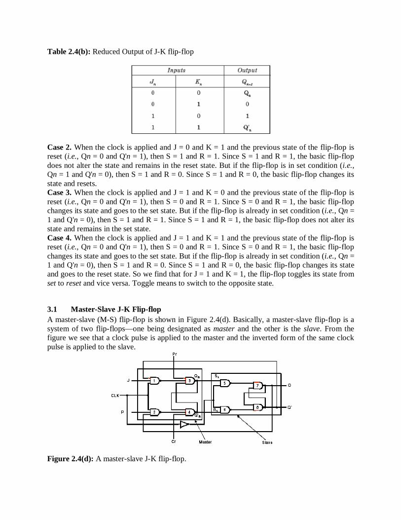
Table 2.4(b): Reduced Output of J-K flip-flop
Case 2. When the clock is applied and J = 0 and K = 1 and the previous state of the flip-flop is reset (i.e., Qn = 0 and Q'n = 1), then S = 1 and R = 1. Since S = 1 and R = 1, the basic flip-flop does not alter the state and remains in the reset state. But if the flip-flop is in set condition (i.e., Qn = 1 and Q'n = 0), then S = 1 and R = 0. Since S = 1 and R = 0, the basic flip-flop changes its state and resets. Case 3. When the clock is applied and J = 1 and K = 0 and the previous state of the flip-flop is reset (i.e., Qn = 0 and Q'n = 1), then S = 0 and R = 1. Since S = 0 and R = 1, the basic flip-flop changes its state and goes to the set state. But if the flip-flop is already in set condition (i.e., Qn = 1 and Q'n = 0), then S = 1 and R = 1. Since S = 1 and R = 1, the basic flip-flop does not alter its state and remains in the set state. Case 4. When the clock is applied and J = 1 and K = 1 and the previous state of the flip-flop is reset (i.e., Qn = 0 and Q'n = 1), then S = 0 and R = 1. Since S = 0 and R = 1, the basic flip-flop changes its state and goes to the set state. But if the flip-flop is already in set condition (i.e., Qn = 1 and Q'n = 0), then S = 1 and R = 0. Since S = 1 and R = 0, the basic flip-flop changes its state and goes to the reset state. So we find that for J = 1 and K = 1, the flip-flop toggles its state from set to reset and vice versa. Toggle means to switch to the opposite state.
3.1 Master-Slave J-K Flip-flop A master-slave (M-S) flip-flop is shown in Figure 2.4(d). Basically, a master-slave flip-flop is a system of two flip-flops—one being designated as master and the other is the slave. From the figure we see that a clock pulse is applied to the master and the inverted form of the same clock pulse is applied to the slave.
Figure 2.4(d): A master-slave J-K flip-flop.

When CLK = 1, the first flip-flop (i.e., the master) is enabled and the outputs Qm and Q'm respond to the inputs J and K. At this time the second flip-flop (i.e., the slave) is disabled because the CLK is LOW to the second flip- flop. Similarly, when CLK becomes LOW, the master becomes disabled and the slave becomes active, since now the CLK to it is HIGH. Therefore, the outputs Q and Q' follow the outputs Qm and Q'm respectively. Since the second flip-flop just follows the first one, it is referred to as a slave and the first one is called the master. Hence, the configuration is referred to as a master-slave (M-S) flip-flop. In this type of circuit configuration the inputs to the gates 5 and 6 do not change at the time of application of the clock pulse. Hence the race-around condition does not exist. The state of the master-slave flip-flop, shown in Figure 2.4(d), changes at the negative transition (trailing edge) of the clock pulse. Hence, it becomes negative triggering a master-slave flip-flop. This can be changed to a positive edge triggering flip-flop by adding two inverters to the system—one before the clock pulse is applied to the master and an additional one in between the master and the slave. The logic symbol of a negative edge master-slave is shown in Figure 2.4(e). The system of master-slave flip-flops is not restricted to J-K master-slave only. There may be an S-R master-slave or a D master-slave, etc., in all of them the slave is an S-R flip-flop, whereas the master changes to J-K or S-R or D flip-flops.
Figure 2.4(e): A negative edge-transition master-slave J-K flip-flop.
3.2 T Flip-Flop With a slight modification of a J-K flip-flop, we can construct a new flip-flop called a T flip-flop. If the two inputs J and K of a J-K flip-flop are tied together it is referred to as a T flip-flop. Hence, a T flip-flop has only one input T and two outputs Q and Q'. The name T flip-flop actually indicates the fact that the flip-flop has the ability to toggle. It has actually only two states—toggle state and memory state. Since there are only two states, a T flip-flop is a very good option to use in counter design and in sequential circuits design where switching an operation is required. The truth table of a T flip-flop is given in Table 2.4(c). Table 2.4(c): The truth table of a T flip-flop