bendability optimization of flexible optical...
TRANSCRIPT

Lee et al. Nanoscale Research Letters 2012, 7:256http://www.nanoscalereslett.com/content/7/1/256
NANO EXPRESS Open Access
Bendability optimization of flexible opticalnanoelectronics via neutral axis engineeringSangmin Lee1†, Jang-Yeon Kwon2†, Daesung Yoon3, Handong Cho1, Jinho You3, Yong Tae Kang3, Dukhyun Choi3*
and Woonbong Hwang1*
Abstract
The enhancement of bendability of flexible nanoelectronics is critically important to realize future portable and wearablenanoelectronics for personal and military purposes. Because there is an enormous variety of materials and structures thatare used for flexible nanoelectronic devices, a governing design rule for optimizing the bendability of these nanodevicesis required. In this article, we suggest a design rule to optimize the bendability of flexible nanoelectronics through neutralaxis (NA) engineering. In flexible optical nanoelectronics, transparent electrodes such as indium tin oxide (ITO) are usuallythe most fragile under an external load because of their brittleness. Therefore, we representatively focus on thebendability of ITO which has been widely used as transparent electrodes, and the NA is controlled by employing a bufferlayer on the ITO layer. First, we independently investigate the effect of the thickness and elastic modulus of a buffer layeron the bendability of an ITO film. Then, we develop a design rule for the bendability optimization of flexible opticalnanoelectronics. Because NA is determined by considering both the thickness and elastic modulus of a buffer layer, thedesign rule is conceived to be applicable regardless of the material and thickness that are used for the buffer layer. Finally,our design rule is applied to optimize the bendability of an organic solar cell, which allows the bending radius to reachabout 1 mm. Our design rule is thus expected to provide a great strategy to enhance the bending performance of avariety of flexible nanoelectronics.
Keywords: Flexible optical nanoelectronics, Bendability optimization, Neutral axis engineering, Buffer layer
BackgroundThere has been rapid development in the field of flexibleoptical nanoelectronics such as organic solar cells (OSCs)and organic light-emitting diodes for future portable andwearable electronic nanodevices, which have potentialpersonal and military applications [1-10]. These opticalnanodevices basically require an optically transparent win-dow to absorb or emit light. Indium tin oxide (ITO) thinfilms have been widely used as transparent electrodes forsuch optical nanoelectronics because of their high visibletransparency, chemical stability, and excellent adhesion toa substrate [11-13]. However, despite its advantages, ITO
* Correspondence: [email protected]; [email protected]†Equal contributors1Department of Mechanical Engineering, Pohang University of Science andTechnology, San 31, Hyoja, Namgu, Pohang, Gyungbuk 790-784, Republic ofKorea3Department of Mechanical Engineering, College of Engineering, Kyung HeeUniversity, 1 Seocheon-dong, Giheung-gu, Yongin-si 446-701, Republic ofKoreaFull list of author information is available at the end of the article
© 2012 Lee et al.; licensee Springer. This is an OAttribution License (http://creativecommons.orin any medium, provided the original work is p
is still difficult to apply to flexible optical nanodeviceswithout damaging the electronic functionality under anexternal bending load because of its brittleness. Research-ers are thus trying to find substitutes for ITO such as car-bon nanotube, graphene, and aluminum-doped zinc oxide(AZO) [10,12-14]. However, with these alternatives, it isstill difficult not only to successfully achieve a high-qualityand low-cost production that is as good as ITO with hightransparency (higher than 90 %) and low electric resist-ance (less than 10Ω), but also to successfully increasebendability due to their brittleness which is common withITO. Thus, it is critically necessary to develop innovativeideas and solutions to enhance mechanical stability ofITO under external bending loads.To improve the bendability of flexible nanoelectronics, a
buffer layer has been adopted [3,6,9,15]. Researchers havereported that the mechanical bendability of electronicnanodevices can be increased by using a buffer layer aboveor below the ITO layer. However, they did not suggest anoptimized design rule that considers both the thickness
pen Access article distributed under the terms of the Creative Commonsg/licenses/by/2.0), which permits unrestricted use, distribution, and reproductionroperly cited.

Lee et al. Nanoscale Research Letters 2012, 7:256 Page 2 of 7http://www.nanoscalereslett.com/content/7/1/256
and elastic modulus of the buffer material. Because vari-ous buffer layers could be used to increase the thermal,chemical, and mechanical stabilities of flexible electronicnanodevices, a governing design rule is crucially needed tooptimize the bendability of these flexible nanodevices re-gardless of the buffer layers that are chosen. In this article,we report a design rule for the bendability optimization offlexible optical nanoelectronics through controlling theneutral axis (NA). If we place the fragile layer such as ITOin a nanodevice at the NA position, the bending stress andstrain in the layer are greatly reduced, thus enhancing thebendability of the device. Therefore, we first investigatethe behavior of the NA position and the effect on the de-vice bendability by independently considering the elasticmodulus and thickness of a buffer layer on the ITO. Be-cause the elastic modulus and thickness of a buffer layerinfluenced each other when determining the NA, weshould consider these parameters together. Therefore, wedevelop a design rule for the bendability optimization offlexible electronics by controlling the NA position, consid-ering both the thickness and elastic modulus of the bufferlayer. Finally, our design rule to optimize the bendabilityof flexible devices is applied to an inverted OSC with anITO optical window. We believe that our design rulebased on NA engineering will provide a great advantageto improve the bendability of flexible nanoelectronics.
MethodsBending theoryFigure 1 shows a cross-sectional illustration of the stressdistribution of an ITO film by controlling NA. The
Figure 1 Scheme for NA positions of a flexible film including abrittle material (here, ITO). (a) Without and (b) with a buffer layer.By adopting a buffer layer, NA can be controlled to be located tothe brittle material, leading to high bendability. (c, d) Illustrations ofcorresponding stress distributions for (a) and (b), respectively. (E:elastic modulus, t: thickness, T: tensile stress, C: compressive stress).
position of the NA is determined from the condition thatthe resultant axial force acting on the cross section is zero:
ZAσAdA ¼ 0 ð1Þ
where σ is the longitudinal stress and dA is the element ofcross-sectional area. The strain (E) curvature relation inpure bending is
E ¼ � yρ¼ �κy ð2Þ
where y is the distance from the NA, ρ is the bending ra-dius, and κ is the curvature. The most common stress–strain relationship encountered in engineering is the equa-tion for a linearly elastic material. For such materials, wesubstitute Hooke's law for uniaxial stress into Equation 2and obtain
σ ¼ EE ¼ �Eκy ð3ÞIn this equation, the normal stresses acting on the cross
section are proportional to the distance, y, from the NA ata given κ. Thus, it is important to locate the most fragilematerial at the NA position to minimize the stress appliedto the material. As shown in Figure 1a,b, when there arehomogeneous films with a symmetric cross section, such asITO and a substrate, we compared the maximum bendingstresses of ITO films without and with a buffer layer. Basedon Equation 3, the maximum bending stress of the ITOwith a buffer layer can be significantly decreased more thanthat of the ITO without a buffer layer because y2 << y1, asshown in Figure 1c,d. In other words, by adopting a bufferlayer, a fragile layer such as ITO can be located at the NAposition and the bending stress acting on the fragile layercan be greatly reduced, thus leading to flexible nanoelectro-nics with high bendability.
Results and discussionTo investigate the bendability of a nanodevice accordingto the NA position, the elastic properties for each mater-ial should be determined. The elastic modulus of thinlayers can be measured by using standard nano-indentation techniques. These techniques depend on thefact that the displacements recovered during unloadingare largely elastic, which allows the Oliver and Pharrmethod to be used to determine the modulus from ananalysis of indentation load–displacement data [16-19].The load (P) and displacement (h) are measured directlyfrom the indentation load–displacement curve, as shownin Figure 2a, and the contact stiffness (S) is determinedby measuring the unloading slope at peak load. If thevalues are determined, we can obtain the elastic modu-lus for each material by using the analysis procedure ofthe Oliver and Pharr method [16]. Four specimens,
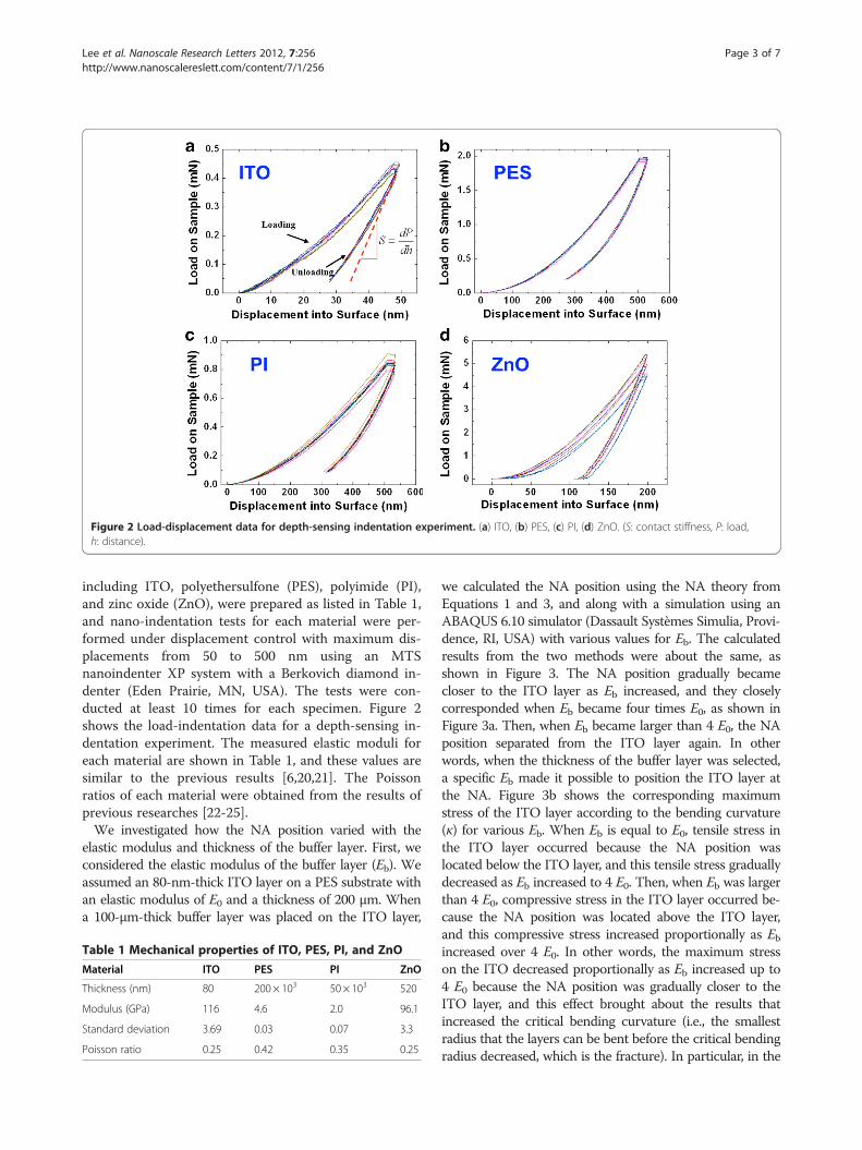
Figure 2 Load-displacement data for depth-sensing indentation experiment. (a) ITO, (b) PES, (c) PI, (d) ZnO. (S: contact stiffness, P: load,h: distance).
Lee et al. Nanoscale Research Letters 2012, 7:256 Page 3 of 7http://www.nanoscalereslett.com/content/7/1/256
including ITO, polyethersulfone (PES), polyimide (PI),and zinc oxide (ZnO), were prepared as listed in Table 1,and nano-indentation tests for each material were per-formed under displacement control with maximum dis-placements from 50 to 500 nm using an MTSnanoindenter XP system with a Berkovich diamond in-denter (Eden Prairie, MN, USA). The tests were con-ducted at least 10 times for each specimen. Figure 2shows the load-indentation data for a depth-sensing in-dentation experiment. The measured elastic moduli foreach material are shown in Table 1, and these values aresimilar to the previous results [6,20,21]. The Poissonratios of each material were obtained from the results ofprevious researches [22-25].We investigated how the NA position varied with the
elastic modulus and thickness of the buffer layer. First, weconsidered the elastic modulus of the buffer layer (Eb). Weassumed an 80-nm-thick ITO layer on a PES substrate withan elastic modulus of E0 and a thickness of 200 μm. Whena 100-μm-thick buffer layer was placed on the ITO layer,
Table 1 Mechanical properties of ITO, PES, PI, and ZnO
Material ITO PES PI ZnO
Thickness (nm) 80 200× 103 50 × 103 520
Modulus (GPa) 116 4.6 2.0 96.1
Standard deviation 3.69 0.03 0.07 3.3
Poisson ratio 0.25 0.42 0.35 0.25
we calculated the NA position using the NA theory fromEquations 1 and 3, and along with a simulation using anABAQUS 6.10 simulator (Dassault Systèmes Simulia, Provi-dence, RI, USA) with various values for Eb. The calculatedresults from the two methods were about the same, asshown in Figure 3. The NA position gradually becamecloser to the ITO layer as Eb increased, and they closelycorresponded when Eb became four times E0, as shown inFigure 3a. Then, when Eb became larger than 4 E0, the NAposition separated from the ITO layer again. In otherwords, when the thickness of the buffer layer was selected,a specific Eb made it possible to position the ITO layer atthe NA. Figure 3b shows the corresponding maximumstress of the ITO layer according to the bending curvature(κ) for various Eb. When Eb is equal to E0, tensile stress inthe ITO layer occurred because the NA position waslocated below the ITO layer, and this tensile stress graduallydecreased as Eb increased to 4 E0. Then, when Eb was largerthan 4 E0, compressive stress in the ITO layer occurred be-cause the NA position was located above the ITO layer,and this compressive stress increased proportionally as Ebincreased over 4 E0. In other words, the maximum stresson the ITO decreased proportionally as Eb increased up to4 E0 because the NA position was gradually closer to theITO layer, and this effect brought about the results thatincreased the critical bending curvature (i.e., the smallestradius that the layers can be bent before the critical bendingradius decreased, which is the fracture). In particular, in the

Figure 3 Behavior of NA position only by considering Eb. (a) NAposition depending on Eb by the NA theory and simulation (red:tension, blue: compression). (b) Maximum stress of ITO layeraccording to κ for various Eb.
Figure 4 Behavior of NA position only by considering the tb ofa buffer layer. (a) NA position depending on tb by the NA theoryand the simulation (red: tension, blue: compression). (b) Maximumstress of ITO layer according to κ for various tb.
Lee et al. Nanoscale Research Letters 2012, 7:256 Page 4 of 7http://www.nanoscalereslett.com/content/7/1/256
case of Eb = 4 E0, when the maximum bending curvaturewas 20 cm−1 (i.e., maximum bending radius was 500 μm),the maximum stress was only about 250 MPa. Consideringthe yield strength of 1.2 GPa for ITO [26], it would not loseits inherent properties up to a critical bending radius of100 μm. In Figure 3, the slight difference in the results be-tween the theory and simulation was probably caused bythe assumption that a cross-sectional area of the beam inthe theory does not change when being bent (i.e., the theorydoes not consider the effect of Poisson's ratio).Next, we considered the effect of the thickness of the buf-
fer layer (tb) on the NA, as shown in Figure 4. We assumedthat an 80-nm-thick ITO layer was on a PES substrate withE0 and a thickness of 200 μm. When Eb was the same as E0,the NA position was calculated with various values for tbusing the two methods mentioned above. When tb waslower than t0, the NA position was located below the ITOlayer, and the tensile stress in the ITO layer occurred. TheNA position became closer to the ITO layer as tb increasedup to t0, and this corresponding tensile stress graduallydecreased. Then, when tb was larger than t0, the ITO layerwas located above the NA position, and the compressivestress in the ITO layer occurred. This compressive stressincreased proportionally as tb increased over t0, as shown in
Figure 4a. In the case of tb = t0, considering the yieldstrength of ITO, the critical bending curvature was about60 cm−1 (i.e., the bending radius was about 167 μm), asshown in Figure 4b. Thus, by controlling the elastic modu-lus and thickness of a buffer layer, the NA position couldbe easily controlled, and the mechanical bending stabilityof the ITO layer could be significantly increased whenthe ITO layer was located at the NA position. In order toconfirm the theoretical behavior of the NA and the corre-sponding mechanical durability, we performed an experi-ment in which the electrical resistance of ITO films wasmeasured as the bending curvature increased. PI wasadopted as a buffer layer on an ITO film (see the inset inFigure 5a), and we increased the tb of PI from 0 to 250 μm.The PI thickness was simply controlled using a PI adhesivetape with a thickness of 50 μm, and we confirmed that theelastic modulus of the PI film does not change by thenano-indentation test when the thickness increased from50 to 250 μm. Figure 5a shows the dependence of the two-probe resistance for PI(tb)/ITO/PES on bending curvatureκ, and R/R0 indicates the bent-to-unbent ratio of the two-probe resistance. The initial curvature of all the structureswas almost flat up to 0.7 cm−1. When the curvature washigher than 0.7 cm−1, the resistance for all of the structures

Figure 5 Experimental verification of enhanced bendability ofITO-based thin films according to the tb of PI. (a) Two-proberesistance and (b) maximum stress of ITO layer for PI/ITO/PES onbending curvature κ (σy: yield strength).
Figure 6 Relationship between Eb and tb. Considering a simplemultilayer model composed of three kinds of materials includingsubstrate (E0, t0), ITO (EI, tI), and buffer layer (Eb, tb).
Lee et al. Nanoscale Research Letters 2012, 7:256 Page 5 of 7http://www.nanoscalereslett.com/content/7/1/256
increased. As the thickness of the buffer layer increased,the change in resistance decreased. In particular, in thecase of a buffer layer with a thickness of 250 μm, the re-sistance was almost zero up to a curvature of 1 cm−1.Then, the resistances for structures with buffer layer thick-nesses of 0, 50, and 150 μm could not be obtained for cur-vatures of 1, 1.2, and 2.5 cm−1, respectively. This wascaused by a fracture of the ITO layer in the structures.Thus, we confirmed that the bendability of the ITO filmcould be increased by employing a buffer layer, and thiswas because the maximum bending stress of the ITO layerwas decreased by locating the ITO layer near the NA pos-ition based on Equation 3.Again, to confirm these results, we performed a simula-
tion of the PI(tb)/ITO/PES structure to determine how themaximum bending stress of ITO changed with the bufferlayer thickness. Based on the simulated results, we foundwhen the fracture of the ITO layer occurred for each speci-men and compared the simulated results with the experi-mental results. As shown in Figure 5b, the yield of ITOlayers consisting of a buffer layer with thicknesses of 0, 50,and 150 μm respectively occurred at curvatures of about
1.1, 1.3, and 2.6 cm−1, and these results were in close agree-ment with those of the experiment. However, the structureswith a buffer layer showed relatively high-level resistanceswhen the bending curvature was larger than 1 cm−1 (i.e., R/R0 were greater than 100). This might be caused by the im-perfect bonding of the buffer layer because the PI adhesivetapes were not firmly bound to one another when thethickness was increased. Even though the structures with abuffer layer showed relatively high resistance, for the above-mentioned reason, the simulation and experiment demon-strated that ITO-based structures with a buffer layer arehighly reliable and durable during bending. As stated earl-ier, to significantly increase the bendability of flexibledevices, we should place the ITO layer at the NA position.So far, although we independently considered the effects
of Eb and tb, when the other was fixed, all of them depend-ently had an influence on the NA position. Thus, it is ne-cessary to develop the governing design rule for thebendability optimization, considering the relationship be-tween them. To deduce this relationship, we considered asimple multilayer model composed of three kinds of mate-rials, including the substrate (E0, t0), ITO (EI, tI), and bufferlayer (Eb, tb), as shown in Figure 6 (inset). From Equations 1and 3, the equation for locating the NA becomes
Eb
ZbydAþ EI
ZIydAþ E0
Z0ydA ¼ 0 ð4Þ
Assuming that the NA is at the center of the ITO, thisequation can be obtained by substituting the expressionsfor y and A into the expressions for t and w; thus,
Ebtb þ tI
2
� �tbwþ EI 0ð Þtbw� E0
t0 þ tI2
� �t0w ¼ 0 ð5Þ
where A and w are the cross-sectional area and width, re-spectively. Because the ITO layer for optical electronics is

Figure 7 Critical bending radius for inverted OSCs. Composed ofvarious buffer materials with thickness optimized by the design rulebased on NA engineering.
Lee et al. Nanoscale Research Letters 2012, 7:256 Page 6 of 7http://www.nanoscalereslett.com/content/7/1/256
very thin (tI << t0, tb), we can set tI to zero. Thus, the re-lationship between Eb and tb is as follows:
Ebt2b ¼ E0t
20 ð6Þ
Equation 6 can be solved for tb in terms of Eb, obtain-ing the following relationship:
tb ¼ t0ffiffiffiffiffiE0
p� 1ffiffiffiffiffi
Ebp ð7Þ
This equation shows that tb is inversely proportionalto the square root of Eb, as shown in Figure 6. Thisequation provides the design rule that can optimize thebendability of flexible optical nanoelectronics by tuningboth the elastic modulus and thickness of a buffer layer.In other words, when designing flexible optical electron-ics, we can choose a specific material of any thicknessand improve not only the mechanical bendability, butalso the electrical efficiency. Because there is an enor-mous variety of materials and structures in flexible elec-tronics, our design rule can have a great effect on thesedevices. Even though we assumed that one fragile layerexists between the substrate and buffer layer, this designrule can be applied to optical nanoelectronics with mul-tiple fragile layers such as conductive oxides, includingITO, ZnO, and AZO, because the thickness of the con-ductive oxides for optical electronics is typically lessthan a few hundred nanometers and all fragile layers arelocated near the NA. Although the multiple layers existin OSCs, their effect in Equation 5 is very small and isnegligible. Thus, we can obtain the optimized thicknessof each buffer layer from Equation 7 when the bufferlayers with various material properties are respectivelyemployed.To demonstrate our design rule for the bendability
optimization of flexible electronics with multiple fragilelayers, we applied different buffer materials (polycarbonate(PC), PI, poly(methyl methacrylate) (PMMA), and poly-styrene (PS)) to inverted OSCs with an ITO optical win-dow. The inverted OSC was composed of five layers,including PES (200 μm), ITO (80 nm), ZnO (50 nm), poly(3-hexylthiophene)/[6,6]-phenyl-C61-butyric acid methylester blend photoactive layer (E=6.02 GPa, ν= 0.35,t=100 nm), and Au (E= 69.8 GPa, ν= 0.44, t=70 nm)[27,28]. To optimize the bendability of flexible electronics,the thickness of each buffer material was calculated basedon the elastic modulus of buffer layers from Equation 7.The optimized thicknesses of PC, PI, PMMA, and PS were278, 303, 236, and 247 μm, respectively. Figure 7 showsthe critical bending radius (ρc) for inverted OSCs with dif-ferent buffer materials from the simulation, consideringthe yield strength for each material (σy = 200 MPa for ZnOand σy = 120 MPa for Au) [29]. While the ρc of the devicewith no buffer layer was only about 2.2 cm due to a
fracture of Au, the ρc of each device with the buffer mater-ial, including optimized PC, PI, PMMA, and PS, were1.11, 1.11, 1.09, and 1.05 mm, respectively. All of theinverted OSCs with different buffer materials to which ourdesign rule was applied had almost the same ρc, whichwas at least 20 times lower than that with no buffer layer.These results clearly showed that our design rule couldoptimize the bendability of flexible nanoelectronics withvarious buffer materials. Further, the ρc of each compo-nent in the device without a buffer layer such as Au, ITO,and ZnO varied from 2.2 to 0.34 cm, depending on theirmaterial properties, whereas in the case of the device witha buffer layer, ρc values of the components were on a simi-lar level (i.e., low ρc), regardless of their properties. Thiswas because all of the thin fragile components werelocated near the NA position, and this result clearlyshowed that our design rule can also be applied to flexibleoptical nanodevices with multiple thin, fragile layers. Inother words, no matter what buffer materials and thincomponents are used in the devices, the bendability canbe significantly enhanced by the design rule based on NAengineering. Thus, this design rule could provide valuableguidance for the design and performance optimization offlexible optical nanoelectronics.
ConclusionsIn summary, we have clearly demonstrated that thebendability of flexible optical nanodevices could be sig-nificantly enhanced by NA engineering, considering boththe thickness and elastic modulus of a buffer layer onthe ITO layer. Because the material property and geom-etry of a buffer layer could be different based on the pur-pose of a flexible electronic nanodevice, our design rule,which considers both the thickness and modulus of abuffer layer, is anticipated to be suitable for the

Lee et al. Nanoscale Research Letters 2012, 7:256 Page 7 of 7http://www.nanoscalereslett.com/content/7/1/256
bendability optimization of various flexible nanoelectro-nics. Furthermore, our design rule was applied toinverted OSCs with various buffer materials, and weconfirmed that all of the OSCs showed excellent bend-ability, whatever buffer materials were chosen. Thus, ourstrategy may provide a wide range of opportunities for avariety of flexible electronic applications.
Competing interestsThe authors declare that they have no competing interests.
AcknowledgmentsThis work was supported by the National Research Foundation of Korea(NRF) grant funded by the Ministry of Education, Science and Technology(MEST) (Nos. 2010–0029120 and 2010–0018457), the Basic Science ResearchProgram through the NRF funded by the MEST (2011–0008589), and a grant(Code No. 2011–0032154) from the Center for Advanced Soft Electronicsunder the Global Frontier Research Program of MEST. DC also acknowledgesthe financial supports by the Energy International Collaboration Research &Development Program of the Korea Institute of Energy TechnologyEvaluation and Planning (KETEP) funded by the Ministry of KnowledgeEconomy (MKE) (2011–8520010050) and by the Business for CooperativeR&D between Industry, Academy, and Research Institute funded Korea Smalland Medium Business Administration in 2011 (Grant No. 48401).
Author details1Department of Mechanical Engineering, Pohang University of Science andTechnology, San 31, Hyoja, Namgu, Pohang, Gyungbuk 790-784, Republic ofKorea. 2School of Integrated Technology, Yonsei University, 162-1, Songdo-dong Yeonsu-gu, Incheon 406-840, Republic of Korea. 3Department ofMechanical Engineering, College of Engineering, Kyung Hee University, 1Seocheon-dong, Giheung-gu, Yongin-si 446-701, Republic of Korea.
Authors’ contributionsSL and J-YK equally contributed to this work. WH and DC conceived theinitial idea and designed the schemes. SL, J-YK, and DY performed thenumerical simulations, and HC and JY performed the experiments. WH, DC,J-YK, and YTK, with partial contributions from SL, characterized the results.DC and SL wrote the paper with partial contributions of WH and J-YK. Allauthors discussed the results, commented on the manuscript, and approvedthe final manuscript.
Received: 12 February 2012 Accepted: 15 May 2012Published: 15 May 2012
References1. Normura K, Ohta H, Takagi A, Kamiya T, Hirano M, Hosono H: Room-
temperature fabrication of transparent flexible thin-film transistors usingamorphous oxide semiconductors. Nature 2004, 432:488–492.
2. Han L, Song K, Mandlik P, Wagner S: Ultraflexible amorphous silicontransistors made with a resilient insulator. Appl Phys Lett 2010, 96:042111.
3. Sekitani T, Lba S, Kato Y, Noguchi Y, Someya T: Ultraflexible organicfield-effect transistors embedded at a neutral strain position. Appl PhysLett 2005, 87:173502.
4. Jedaa A, Halik M: Toward strain resistant flexible organic thin filmtransistors. Appl Phys Lett 2009, 95:103309.
5. Zschieschang U, Ante F, Yamamoto T, Takimiya K, Kuwabara H, Ikeda M,Sekitani T, Someya T, Kern K, Klauk H: Flexible low voltage organictransistors and circuits based on a high mobility organic semiconductorwith good air stability. Adv Mater 2010, 22:982–985.
6. Chiang CJ, Winscom C, Bull S, Monkman A: Electroluminescencecharacterization of FOLED devices under two type of external stressescaused by bending. Org Electron 2009, 10:1268–1274.
7. Ju S, Facchetti A, Xuan Y, Liu J, Ishikawa F, Ye P, Zhou C, Marks TJ, Janes DB:Fabrication of fully transparent nanowire transistors for transparent andflexible electronics. Nature Nanotech 2007, 2:378–384.
8. Wang GF, Tao XM, Wang RX: Flexible organic light-emitting diodes with apolymeric nanocomposite anode. Nanotechnology 2008, 19:145201.
9. Sekitani T, Zschieschang U, Klauk H, Someya T: Flexible organic transistorsand circuits with extreme bending stability. Nature Mater 2010,9:1015–1022.
10. Ghosh D, Ghosh P, Tanemura M, Haysahi A, Hayashi Y, Shinji K, Miura N,Yusop MZ, Asaka T: Highly transparent and flexible field emission devicesbased on single-walled carbon nanotube films. Chem Commun 2011,47:4980–4982.
11. Minami T, Yamamoto T, Toda Y, Miyata T: Transparent conductingzinc-co-doped ITO films prepared by magnetron sputtering. Thin SolidFilms 2000, 373:189–194.
12. Yaglioglu B, Yeom HY, Paine DC: Crystallization of amorphous InO–10 wt% ZnO thin films annealed in air. Appl Phy Lett 2005, 86:261908.
13. Minami T: Present status of transparent conducting oxide thin-filmdevelopment for indium-tin-oxide (ITO) substitutes. Thin Solid Films 2008,502:104–106.
14. Wu J, Becerril HA, Bao Z, Liu Z, Chen Y, Peumans P: Organic solar cells withsolution-processed graphene transparent electrodes. Appl Phy Lett 2008,92:263302.
15. Park SK, Han JI, Moon DG, Kim WK: Electrical characteristics of poly(3-hexylthiophene) thin film transistors printed and spin-coated onplastic substrates. Jpn J Appl Phys 2003, 42:623–629.
16. Oliver WC, Pharr GM: Improved technique for determining hardness andelastic modulus using load and displacement sensing indentationexperiments. J Mater Res 1992, 7:1564–1567.
17. Seitzman LE: Mechanical properties from instrumented indentation:uncertainties due to tip-shape correction. J Mater Res 1998, 13:2936–2944.
18. Herrmann K, Jennett NM, Wegener W, Meneve J, Hasche K, Seemann R:Progress in determination of the area function of indenters used fornanoindentation. Thin Solid Films 2000, 377:394–400.
19. Thurn J, Cook F: Simplified area function for sharp indenter tips indepth-sensing indentation. J Mater Res 2002, 17:1143–1149.
20. Lu C, Danzer R, Fischer FD: Scaling of fracture strength in ZnO: effects ofpore/grain-size interaction and porosity. J Eur Ceram Soc 2004,24:3643–3651.
21. James EM: Polymer Data Handbook. New York: Oxford University Press; 1999.22. Kaiyang Z, Furong Z, Jianqiao H, Lu S, Keran Z, Hao G: Investigation on the
origin of green luminescence from laser-ablated ZnO thin film. Thin SolidFilms 2003, 443:60–66.
23. Seitz JT: The estimation of mechanical properties of polymers frommolecular structure. J Appl Polym Sci 1993, 49:1331–1351.
24. Yang PF, Wen HC, Jian SR, Lai YS, Wu S, Chen RS: Characteristics of ZnOthin films prepared by radio frequency magnetron sputtering. MicroelecRelia 2008, 48:389.
25. Qi D, Hinkley J, He G: Molecular dynamics simulation of thermal andmechanical properties of polyimide–carbon-nanotube composites.Modelling Simul Mater Sci Eng 2005, 13:493–507.
26. Bouten PCP, Sikkeveer PJ, Leterrier Y: Mechanics of ITO on plasticsubstrates for flexible displays. In Flexible Flat Panel Displays. Edited byCrawford GP. Chichester: John Wiley & Sons; 2005:99–120.
27. Tahk D, Lee HH, Khang DY: Elastic moduli of organic electronic materialsby the buckling method. Marcromolecules 2009, 42:7079–7083.
28. Diethiker M, Nyilas RD, Solenthaler C, Spolenak R: Nanoindentation ofsingle-crystalline gold thin films: correlating hardness and the onset ofplasticity. Acta Materialia 2008, 56:3887–3899.
29. Chen CQ, Zhu J: Bending strength and flexibility of ZnO nanowires. ApplPhys Lett 2009, 90:043105.
doi:10.1186/1556-276X-7-256Cite this article as: Lee et al.: Bendability optimization of flexible opticalnanoelectronics via neutral axis engineering. Nanoscale Research Letters2012 7:256.