basic of dsp projects
TRANSCRIPT

PROGRAMMEMORY
ComputerEngine
I/O connects
to outside
world
Inside a DSP?
DATAMEMORY
Input / Output
ADC, DAC &PWM Generation
Serial portsTimers
Host portsExternal ports
Link ports


DSP LEADING MANUFACTURERS
1. TEXAS INSTRUMENTS (TI)
2. ANALOG DEVICES (ADSP)
3. MOTOROLA

First DSP Processor : 1982 - General Purpose DSP
23 Years
Current Trend : 2005 - Application Specific DSP
DSP SELECTION CRITERIA
Voltage MigrationPerformancePower ConsumptionPrice
Selecting DSP Processors requires a careful, application specific analysis

TMS320C2000 family offers various DSP processors for motor control. Based on the specific requirements, the user can choose the particular device for the speed control of Induction Motor/Brush less motor/ Switch Reluctance motor. In this platform varieties of DSP Processors are available in 3 categories.
TMS320F240 TMS320F2407 TMS320F2812.
Targeted for Industrial Automation, Automatic Control Application, UPS, Motor Control, etc.
TMS320C2000 PLATFORM

TMS320 DEVICE NOMENCLATURE

DSP BASED MOTOR CONTROL
Motor control is the most challenging field of application for electric drives. Highest performance is required as regards dynamic behavior, steady state accuracy and uniformity of movement. PWM techniques play an important role in satisfying the above demands.
PWM

PULSE WIDTH MODULATOR Pulse width modulation is a series of short
duration output pulses for driving a switch.
By adjusting the on/off period of the PWM we can control the load voltage.
PWM has to be generated either by Analog method or by Digital method.
By applying these PWMs to the IGBT switches, 3 phase sine output are generated to drive an AC Induction Motor.
Various feedback signal is measured for the PWM Generation and correction.

Vc
TriangularWaveformgenerator
Va
Carrier
+V
-V
PWM
_
+
PWM GENERATION BY ANALOG METHOD

ANALOG METHOD OF PWM GENERATION FOR CHOPPER
VoltageSource
CarrierGenerator
DRIVERDELAY
& ISOL-ATION
CIRCUIT
Comparator
Comparator
G1
G2G3
G4

DSP BASED MOTOR CONTROL =
DSP PROCESSING POWER+
CONTROL SPECIFIC PERIPHERALS
DSP FOR MOTOR CONTROL

TI PROCESSORS
Texas instruments offers various processors for motor control applications.processors available are,
TMS320F240TMA320F2407TMS320F2812

TMS320F240 TMS320F2407A TMS320F2812
16 Bit Fixed point 16 Bit Fixed point 32 Bit Fixed point
20 MIPS 40 MIPS 150 MIPS
544 x 16 Bit RAM 2.5k x 16 Bit RAM 18k x 16 Bit RAM
3 GP Timers 4 GP Timers 7 GP Timers
SPI & SCI Serial ports
SPI, SCI & CAN Serial ports
SPI, SCI & CAN Serial ports
12 PWM Channels 16 PWM Channels 16 PWM Channels
16 Channel ADC @ 6 microsec conversion time
16 Channel ADC @ 0.5 micro sec conversion time
16 Channel ADC @ 200 ns conversion time

LF2407 KEY FEATURES 3.3v operating volts
16 bit fixed point processor with 144 pins
40MHz operating frequency
32KWord FLASH memory, 2.5 K Word RAM
40 general-purpose I/O (GPIO) lines
On-chip peripherals
Event manager
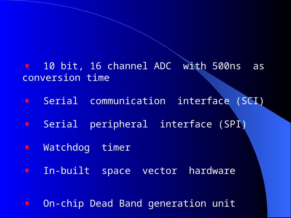
• 10 bit, 16 channel ADC with 500ns as conversion time
• Serial communication interface (SCI)
• Serial peripheral interface (SPI)
• Watchdog timer
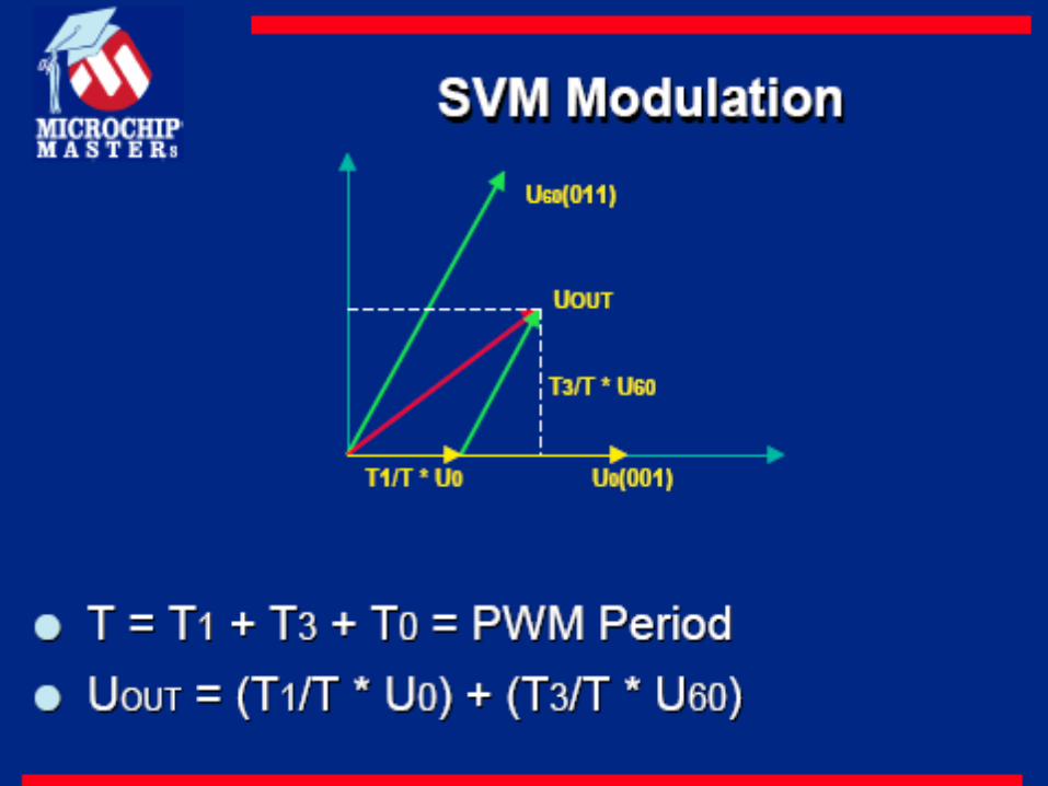
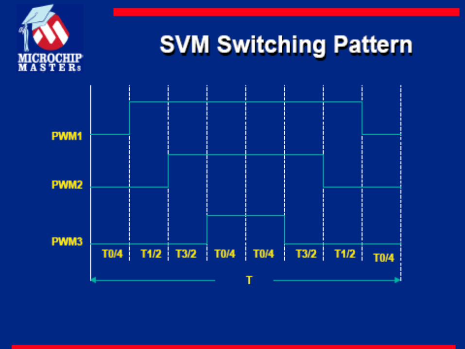
• In-built space vector hardware
• On-chip Dead Band generation unit
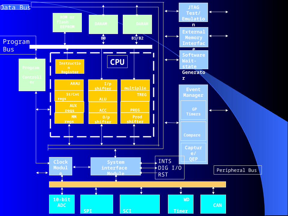
ROM or flash
EEPROM DARAM B0
DARAM B1/B2
Instruction Register
ARAU
St/Cnt regs
AUX regs
MM regs
I/p shifter
ALU
O/p shifter
ACC
multiplier
TREG
Prod shifter
PREG
Program
Controller
Clock Module
System interface Module
JTAG Test/
Emulation
ExternalMemoryInterface
SoftwareWait-stateGenerator
EventManager
GP Timers
Compare Units
Capture/QEP
10-bitADC SPI SCI
WD Timer CAN
Program Bus
Data Bus
Peripheral Bus
INTSDIG I/ORST
CPU

CENTRAL PROCESSING UNIT
A 32-bit central arithmetic logic unit (CALU)
A 32-bit accumulator
Data-scaling shifters
A 16-bit X 16-bit multiplier
A 32-bit product register
8 auxiliary registers and an auxiliary register arithmetic unit

CPU BUS STRUCTUREPAB Program Address Bus provides addresses for both reads
from and writes to program memory
DRAB Data Read Address Bus provides addresses for reads from data memory
DWAB Data Write Address bus provides addresses for writes to data memory
PRDB Program Read Bus carries instruction code and immediate operands as well as table information from program memory to the CPU
DRDB Data Read Bus carries data from data memory to the CALU and ARAU
DWEB Data Write Bus carries data to both program memory and data memory

Multiplication section• 16 bit TREG holds one of the multiplicands• Multiplier multiplies the TREG value from
data or program memory• 32 bit PREG receives the result• Product shifter scales the PREG value before
allow it to CALU
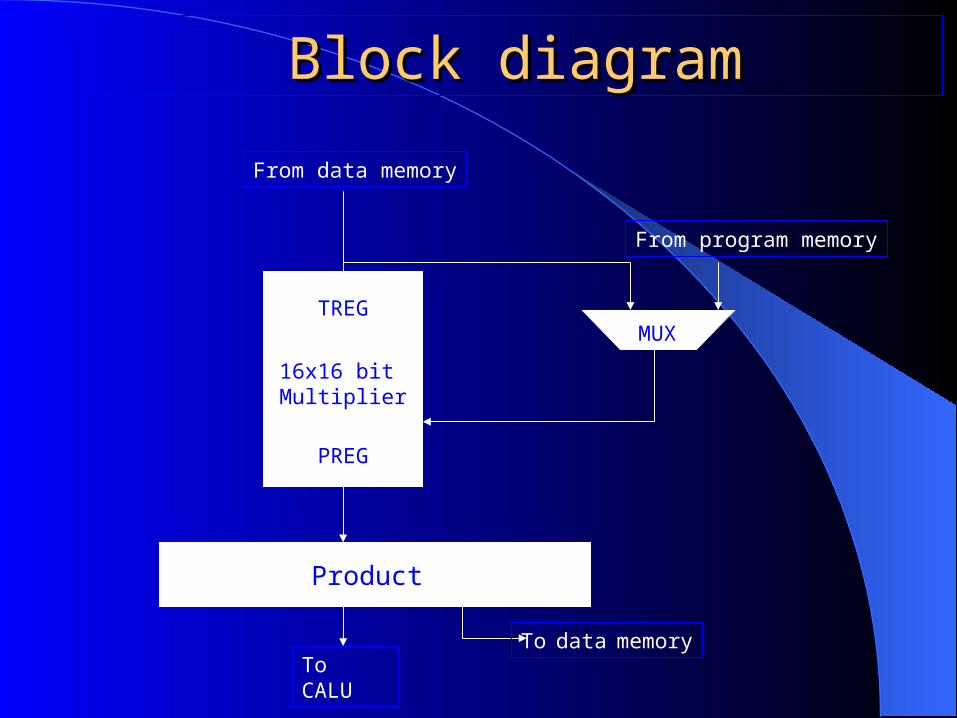
Block diagramBlock diagram
TREG
16x16 bit Multiplier
PREG
32 bit Product shifter
To CALUTo data memory
MUX
From program memory
From data memory

MEMORY
• 544 words * 16 bits of on-chip data/program dual-access RAM
• 32K words * 16 bits of on-chip program Flash EEPROM
• 2K words * 16 bits of single-access RAM
• External memory interface module

PROGRAM MEMORY
Interrupts vectors andreserved addresses
Flash/ ROM 16k/8k words
(External if MP/MC=1)
External
DARAM(256 words)(External if CNF=0)
Reserved
Interrupts level 6
0000
003F0040
3FFF4000FDFFFE00
FEFFFF00
FFFF
ResetInterrupts level 1Interrupts level 2Interrupts level 3
Software interrupts

DATA MEMORY
PAGE 0 : 0000H - 007FH
PAGE 1 : 0080H – 00FFH
PAGE 2 : 0100H – 017FH
PAGE 511 : FF80H - FFFFH
.
.
.
.
.

LF2407 DATA MEMORYTotal memory = 0000h – FFFFh (64KW)Total memory = 0000h – FFFFh (64KW)
Total no. pages = 200hTotal no. pages = 200h
Each page contains 80h wordsEach page contains 80h words
Page 0 = 0h * 80h = 0000 to 007FPage 0 = 0h * 80h = 0000 to 007F
Page 1 = 1h * 80h = 0080 to 00FFPage 1 = 1h * 80h = 0080 to 00FF
.. .. .. .. .. .. .. .. .. .. .. .. .. .. .. .. .. .. Page 100 = 100h * 80h = 8000 to 807FPage 100 = 100h * 80h = 8000 to 807F
Page 1FF = 1FFh * 80h = FF80 to FFFFPage 1FF = 1FFh * 80h = FF80 to FFFF

DATA MEMORY SPACE ALLOCATION
Starting
address
Ending
address
Descripti0n Memory
Type
0000 7FFF
ON-CHIP RAM
RAM
8000 FFFF USER DATA MEMORY
RAM

FLASH REGISTERSRegister Name Description
SEG_CTR(16 bit)
Flash Segment ControlRegister
The 8 MSBs enable specific segments
TST(5 bit)
Flash Test Register Reserved for test & is not accessible during normal operational modes
WADRS(16 bit)
Write Address Register Holds the address for a Write oper.
WDATA(16 bit)
Write Data Register Holds the data for a Write oper

PROGRAM-ADDRESS GENERATION
This process uses the following hardware:
* Program Counter(PC)* Program Address Register(PAR)* Stack* Repeat Counter(RPTC) The stack can be access with two set of instructions, which are:
* PUSH & POP* PUSHD & POPD

ADDRESSING MODESThere are three addressing modes, they are:
• Direct addressing mode• Indirect addressing mode• Immediate addressing mode
DIRECT ADDRESSING MODE:LDP #150 ;set data page to 150LACC 2H ADD 9H,2 ;The contents of the data address 9h are
;left shifted by 2 bit and added to the ;contents of accumulator
SACL 2H
DP = 150 OFFSET = 21 0101 0000 000 0010
Answer is in the address A802

INDIRECT ADDRESSING MODE :
There are 8 Auxiliary registers (AR0 – AR7) provided for flexibleIndirect addressing mode.
MAR * , AR1 ; Load the ARP with 1 to make AR1 the ; current auxiliary register
LT *+ , AR2 ; AR2 is the next auxiliary register; load the content of the address ref. by AR1
MPY * ; in the TREG, add 1 to the content of AR1
IMMEDIATE ADDRESSING MODE :
ADD #1234H, 2 ; Shift the value left by 2 bits; and add to the accumulator

OVERVIEW OF INSTRUCTION SET
• Accumulator, Arithmetic, and Logic Instructions
• Auxiliary Register Instructions
• TREG, PREG, and Multiply Instructions • Branch Instructions • Control Instructions •I/O and Memory Instructions

.mmregs .text
START:
LDP #150H LACC #1111H ADD #2222H SACL 2H
END B END
PROGRAM FOR ADDITION
OUTPUT:ADDRESS - A802ANSWER - 3333

PROGRAM FOR SUBTRACTION
.mmregs .text
START:
LDP #100H LACC #3333H SUB #1111H SACL 0H
END B END
OUTPUT:ADDRESS - 8000ANSWER - 2222

2407 General Applications
• Motor control
• Power supplies
• UPS
• Industrial automations


IPM UNIT