bands and bonds - massachusetts institute of technologydspace.mit.edu/.../0/bands_and_bonds.pdf ·...
TRANSCRIPT

1
BANDS AND BONDSLionel C. Kimerling
CHEMICAL BONDS IN SOLIDS
The chemical bond arises from a redistribution of electronic charge when atoms are brought in close proximity.The bond in a solid results from the superposition of charge densities of all atoms in the system. In an atom allelectrons reside in their ground states at equilibrium. Only a few low lying excited states are typically accessed.The chemical bond in the solid consists of excited electronic configurations which are created to satisfy theconstraints of a minimum energy, semi-infinite solid. These constraints create not only a variation on atomicenergy level structure, but a compromise between the limiting classifications of bonding.These limiting classifications and their compromises are discussed in this section.
Ionic Solids
Ionic solids are compounds which are composed of atoms with large electronegativity differences. They typicallyinvolve the strongly electronegative group VI and VII elements together with an electropositive counterpart. In thelimit of complete charge transfer (closed shells), the structure and properties are those expected from array ofelectrostatically interacting charges. Structure can be predicted from Pauling's radius ratio approach and electricalinsulating behavior is derived from the strongly bound valence electrons (Eg > 3 eV).
The internal energy of the system can be calculated simply and accurately by superimposing the measuredcompressibility relation on the electrostatic interactions of a point charge array as shown in Figure 1.5.
� � � �� �drrepulsiveFattractiveFUr
��
��
� �nRBeRZAeN // 222���� (1.3)
� � ��
���
���n
RZNAe 1122
ijRNZZeattractiveU 21)( ��� (1.4)
where R is the interatomic distance, Z is the ionic charge, A is the Madelung constant, N is Avogadvo's number,B is the repulsive potential coefficient and n is the Born exponent.
_________________________________
Example 1.6
List the first three terms of the Madelung (attractive) potential for NaCl. (1.5)
� �� � � � � �� �21
22
1
2
21
2
32126)( ZZ
reZ
reZZ
reattractiveU �����������
(Na+) (nearest neighbor C1-) (nearest neighbor Na+) (next nearest neighbor C1-)
_________________________________
2
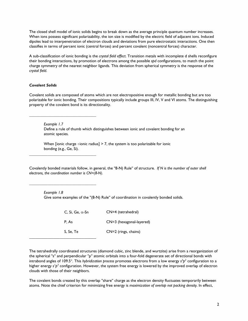
The closed shell model of ionic solids begins to break down as the average principle quantum number increases.When ions possess significant polarizability, the ion size is modified by the electric field of adjacent ions. Induceddipoles lead to interpenetration of electron clouds and deviations from pure electrostatic interactions. One thenclassifies in terms of percent ionic (central forces) and percent covalent (noncentral forces) character.
A sub-classification of ionic bonding is the crystal field effect. Transition metals with incomplete d shells reconfiguretheir bonding interactions, by promotion of electrons among the possible spd configurations, to match the pointcharge symmetry of the nearest neighbor ligands. This deviation from spherical symmetry is the response of thecrystal field.
Covalent Solids
Covalent solids are composed of atoms which are not electropositive enough for metallic bonding but are toopolarizable for ionic bonding. Their compositions typically include groups III, IV, V and VI atoms. The distinguishingproperty of the covalent bond is its directionality.
_________________________________
Example 1.7Define a rule of thumb which distinguishes between ionic and covalent bonding for an atomic species.
When [ionic charge �ionic radius] > 7, the system is too polarizable for ionic bonding (e.g., Ge, Si).
_________________________________
Covalently bonded materials follow, in general, the "8-N) Rule'' of structure. If N is the number of outer shellelectrons, the coordination number is CN=(8-N).
_________________________________
Example 1.8Give some examples of the "(8-N) Rule'' of coordination in covalently bonded solids.
C, Si, Ge, �-Sn CN=4 (tetrahedral)
P, As CN=3 (hexagonal-layered)
S, Se, Te CN=2 (rings, chains)_________________________________
The tetrahedrally coordinated structures (diamond cubic, zinc blende, and wurtzite) arise from a reorganization ofthe spherical "s'' and perpendicular "p'' atomic orbitals into a four-fold degenerate set of directional bonds withintrabond angles of 109.5�. This hybridization process promotes electrons from a low energy s2p2 configuration to ahigher energy s1p3 configuration. However, the system free energy is lowered by the improved overlap of electronclouds with those of their neighbors.
The covalent bonds created by this overlap "share'' charge as the electron density fluctuates temporarily betweenatoms. Note the chief criterion for minimizing free energy is maximization of overlap not packing density. In effect,

3
repulsive forces are determined by the complete inner shell electrons rather than the positively charged nuclearradii.
_________________________________
Example 1.9Contrast covalently bonded structures with metallic and ionically bonded structures.
The covalent structure is more open than the close packed metallic structures and the average electron density varies more slowly between atoms than in the ionic case.
_________________________________
The properties of the covalent solid cannot be treated in the straightforward, analytic fashion of ionic materials.The bond is not truly a local bond. The sharing of the electron density creates extended states of the crystal whichcannot be described as two center excitations. As the assembly of atoms condenses, the degenerate, sharp atomicstates interact and are broadened in energy to a band. (The Pauli exclusion principle prohibits two particles in thesame system from occupying the same energy state.) The band of filled or bonding states is called the valence band.The band of empty or antibonding states is called the conduction band. The highest energy occupied states areseparated from the lowest energy unoccupied states by an energy region containing no states known as thebandgap. The energy difference between the top of the valence band and the bottom of the conduction band is Eg,the gap energy.
At low temperatures all pure semiconductors behave as insulators, because nearly all electrons are participating inbonding. As the temperatures is increased, the electrical conductivity increases with a characteristic activationenergy of Eg/2, reflecting the thermal excitation of carriers from bound to free conduction states.
Metallic Solids
Metallic solids are composed of the electropositive elements of Groups I, II and III. The chemical tendency todonate electrons results in a high CN (8, 12) reflecting predominantly hard sphere repulsive interactions. Thevalence electrons form a continuum which produces cohesion through interaction with the positive ion cores. Thisfree electron gas readily moves through the crystal under the bias of an electric field and produces high electricalconductivity.
In contrast to semiconductors which exhibit an activated conductivity which increases with temperature, metalsexhibit a high conductivity which slowly decreases with temperatures due to carrier scattering by vibrating atomiccores. The density of free carriers is not an activated quantity because the valence band is not filled and emptyconduction states are available with negligible excitation. This same condition is responsible for the characteristicmetallic lustre (high absorption and reflectivity of visible light). The nondirectional nature of the metallic bond leadsto the ductility or ease of plastic deformation of metals.
Mixtures of Group I, II and III elements form alloys, ordered solid solutions and intermetallic compounds. Trendsin the formation of these phases have been delineated by Hume-Rothery and Darken and Gurry. Alloys arecompletely miscible mixtures formed by metal atoms with similar values of atomic radii which crystallize into thesame structure. Ordering occurs in some alloy structures at specific compositions, e.g., AuCu3 . The structure is
characterized by interpenetrating superlattices as expected for a compound, but the distribution changes to that ofa random alloy at high temperatures. Intermetallic compounds form at fixed ratios of constituents and represent atrue metallic phase, e.g., CuZn , 85ZnCu . A special class of intermetallics is the interstitial phase which consists of
a smaller nonmetallic element (B) in the interstices of a metallic (A) structure. These compounds are typicallycarbides, hydrides and nitrides and form when .6.0/ �AB rr

4
Van der Waals Solids
Van der Waals solids consist of inert gas or molecular components. The structure is, typically, close packedreflecting the repulsive potential exhibited by the complete outer electron shells of the constituents. The bondingforces are derived from the Van der Waals interaction which is dipolar in nature. The time variation in electrondensity about an atom produces an oscillation in the center of gravity of the charge which can order cooperativelywith the same process of neighboring atoms to yield a net attractive force. Induced dipole effects of this type areweak but non-negligible. Molecules which possess a permanent dipole exhibit a higher cohesive energy.
Hydrogen Bonded Solids
Hydrogen bonded solids consist primarily of the hydrides of fluorine, oxygen, and nitrogen. The cohesive forcesare derived from the unique nature of the hydrogen bridge bond between two neighboring atoms, which enhancesthe normal intermolecular attraction.
Chemical Trends in Covalent Solids
Primary insights into nature covalent solids are most easily recognized through the Molecular Orbital Approach. Inthis description, the atomic energy levels lose their identity to molecular orbitals of the system. These new orbitalsare composed of hybrids or combinations of the atomic orbitals. As always, the choice of orbital combinationsreflects a minimization of free energy. This minimization is driven, for covalent bonding, by maximization of theoverlap (sharing) of electron density.
The prototypical structure is four fold coordinated with tetrahedral symmetry reflecting sp3 hybridization. Underhydrostatic pressure the atomic constituents are brought closer together and the orbital overlap is no longeroptimal for an sp3 electronic configuration. The s electrons delocalize to a metallic bond and a six fold coordinated,�-Sn (tetragonally distorted, simple cubic) structure is most stable. Table 1.3 lists some properties of the elementalsolids of Group IV. It is evident from the melting points that the covalent bond strength decreases as atomicnumber (or the principal quantum number, n increases. For this isomorphic series, the lattice constant increasesand the energy gap decreases with increasing n. In general, bond strength is inversely proportional to bond lengthand directly proportional to the energy gap.
No trend is evident for the electron mobility. Mobility represents the ability of the electron to accelerate under an
applied electric field ��
���
��
cmVcmunits
/sec/
. This property is, therefore, solely dependent on the mass of the
electron which obviously varies among the materials. This variation is derived from the influence of the periodiclattice potential on the response of the electron. The mass of a free electron in a solid is discussed in terms of aneffective mass m* which is not equal to the universal electron rest mass. Trends and manifestations of m* cannotbe understood without knowledge of the full electronic band structure of the solid.

5
TABLE 1.3
STRUCTURE/COMPOSITION/PROPERTIES OF GROUP IV SOLIDS
Diamond Cubic Structure
MP(�C) ao (Å) Eg (eV) ���
����
�
� sec
2
Vcm
e�
C(diamond) --- 3.56 ~6 1800Si 1410 5.42 1.1 1600Ge 936 5.66 0.72 4400Sn(gray) 232 6.45 0.08 2000Pb <-------------------metallic------------------- >
Compound semiconductors show the same trends as the Group IV elemental materials. Of equal interest are thetrends among the compounds in comparison to the elementals. The structure is tetrahedral, CN=4 zinc blende(cubic) or wurtzite (hexagonal). In the wurtzite structure the next nearest neighbor position is slightly closer thanfor the zinc blende structure. A greater screening of opposite charges takes place, favoring wurtzite where a moreelectronegative constituent (charge transfer) is involved. Table 1.4 lists the structures of the III-V compoundsemiconductors.
TABLE 1.4
STRUCTURES OF III-V COMPOUNDS
W = wurtzite (hexagonal)ZB = zinc blende (cubic)
N P As Sb
B - ZB ZB -Al W ZB ZB ZBGa W ZB ZB ZBIn W ZB ZB ZBTl - - metallic metallic
Structurally, the compound semiconductors are distinguished by crystallographic polarity. Figure 1.5 illustrates howthe termination of the (111) surfaces depends on orientation. The driving force for this configurational property isthe high energy contribution of an unsatisfied bond. By terminating the bottom plane with group V(B) rather thangroup III(A) atoms, one rather than three unsatisfied bonds are exposed. The manifestations of this polarity arekey to the control of epitaxial growth and chemical etching procedures.
Table 1.5 lists a comparison of elemental and compound semiconductors having the same principal quantumnumber. The compounds exhibit a higher melting point, a larger bandgap and similar lattice constants. The lateral(row in Periodic Table) trend toward larger bandgaps continues into the II-VI compounds. This phenomenon isevidence of the mixed (ionic/covalent) nature of the polar covalent bond. The bandgap, Eg, increases with changetransfer (ionicity), even though the average principal quantum number, n , remains constant.

6
TABLE 1.5
COMPOSITION/STRUCTURE/PROPERTIESGroup IV/III-V Compounds
III IV V PropertiesM.P.(ºK)
(IV/III-V)Eg (eV)
ao(Å)
B C N ------------- 6/10 3.56/3.16AI Si P 1685/1770 1.1/3 5.42/5.46Ga Ge As 1231/1510 0.72/135 5.66/5.65In Sn Sb 508/798 0.08/0.18 6.45/6.09
Figure 1.5

7
]211[
[ 111 ]
Figure 1.6ZINC BLENDE STRUCTURE

ENERGY BANDS IN SOLIDS
When separate atoms bind together in a single system to form a solid, their electronic structure is perturbed bythe bonding interaction. For a given structure this change in configuration must satisfy two primary constraints: 1) the Pauli exclusion principle and 2) the periodic lattice potential of the atomic cores.
As shown in Figure 1.7 the identical one electron states of the hydrogen atom form two distinct states uponformation of the H2 molecule. Likewise an array of six atoms must possess six new states for each original atomicstate. This behavior follows because two electrons cannot occupy the same state in the same system (Pauliexclusion principle). Therefore, discrete atomic levels broaden into a band of levels. Since the typical solidcontains ~1022 atoms/cm3 (Si has 5x10²² atoms/cm3), a nearly continuous distribution of energies results. The"shape" of the bands of electron states are determined by the finite size of the solid and the periodic array ofpotentials contained therein.
Sommerfeld proposed in 1928 that free electrons in a solid should behave as a 'particle in a box'. Solution of thewave equation determines the allowed energies as
mkhE
2
22�
�
�
�2��
hpk�
�
where m is the mass of the electron, p� is the electron momentum, and k�
is the electron
predicts one continuous band of energies whose allowed values vary quadratically with k�
The Sommerfeld model is instructive, but fails to consider that the potential energy of an zero. The charge located at each lattice site presents a periodically varying potential whicfrom the crystal in the same manner that an x-ray wave is diffracted at the Bragg conditioscatters off the lattice points as it moves.
When the electron wavelength matches the condition that its maxima or minima occur atby a distance a, n� = 2a, constructive interference occurs and standing waves are createdmust have zero velocity and, hence, cannot exist in the crystal. Two standing waves markforbidden energy region: one associated with the lattice potential minima and one associapotential maxima. As the lattice potential becomes deeper, the "energy gap" widens.
The electron wavelength is formally discussed in terms of its wave vector, �
�2�k . The
wavepacket is described by the term rkie�
�
� . The electron momentum p� is related to k�
de Broglie relation, � = h/p. Thus,
khp�
�
�
The mass of the electron, as for any particle, can be calculated as the second derivative oto its momentum.
(1.6)
(1.7)
8
wave vector. The theory
.
electron in a solid is noth excludes certain statesn. The electron wave
lattice points separated. An electron in this sate the boundary of thisted with the lattice
motion of the electron
through the
(1.8)
f its energy with respect

9
22
2
/*
kdEdhm �� (1.9)
The term m* is used to denote that the electron mass in a solid is not the same as the mass of a free electron.This difference in character is a consequence of the band distortion which is introduced by the periodic potential(energy gaps).
Figure 1.11 shows the discontinuities introduced into the free electron band scheme at the standing wavecondition. Several important observations can be made regarding the electron mass and, hence, its ease of motion.
The band curvature (second derivative) is both positive and negative. Therefore, the electron mass can be bothpositive and negative. This result, practically, describes a particle which may respond both positively and negativelyto the acceleration of an applied electric field. In real terms the positive mass is that of the negatively chargedelectron and the negative mass corresponds to a positively charged hole. In semiconductors mobile electrons occupyempty states at the bottom of the conduction band. Mobile holes occupy states at the top of the valence band which, in aperfect crystal, would be filled with bonding electrons.
The motion of a positively charged hole is, therefore, the motion of a bonding electron state which is empty. Thepositive nature of the carrier is manifested in its acceleration vector under an electronic field, which is opposite tothat of an electron.
A second observation relates the curvature at the band edge discontinuity to the size of the energy gap. As thegap increases, the curvature will decrease, i.e., the effective mass, m*, will increase. Thus, for a series ofsemiconductor compounds with similar lattice constants and band structures, the mobility is expected increase withdecreasing energy gap.
Table 1.6 lists the maximum mobilities, measured at low temperatures, and the energy gaps of some common III-Vcompound semiconductors. This result follows because a smaller energy gap implies lattice scattering potentialwhich allows more free electron flow. This trend is most easily observed for direct gap semiconductors. A directgap material is one in which the minimum energy gap between the valence band and conduction band occurs at single value
of k�
.
An indirect gap material is one in which the maximum for the uppermost filled valence band occurs at a different
k�
than the minimum of the lowest empty conduction band. In an indirect material the energy gap need bear norelation to the curvature of the band extrema.
Figure 1.12 shows the band structures for silicon, an indirect gap semiconductor, and gallium arsenide, a direct gapsemiconductor. The presentation of the band structure in this way exhibits two new features which are added forvisual efficiency.
The periodic nature of k�
allows folding of values greater than �/a back into the same zone. This presentation iscalled the reduced zone scheme.
Since the crystal lattice is not a homogeneous, isotropic medium, the E vs k�
dispersion relations are dependent
on direction within the crystal. An increase in the vector product k�
corresponds to a change in direction and,
thus, the zone edge (integral, an�2
) values of k�
correspond to high symmetry directions of the crystal lattice.
The vector nature of k�
is essential in describing the three dimensional crystal lattice potential.

10
The intrinsic electrical and optical properties of semiconductor materials are determined by the highest filled band,the valence band, and the lowest empty band, the conduction band. In the valence band all electrons are involvedin localized bonding states and are not free to move. Electrons in the lower energy, filled bands are the atomiccore electrons which are even more localized and tightly bound than those in the valence band.
The conduction band in any material is the lowest energy empty or partially filled band (see Fig. 1.13). Carrierswhich occupy states in the conduction band require no activation energy to move and, hence, acquire a kinetic
energy (E) in response to an electric field )(E�
of ��
x
o
dxEE�
. This result follows because an empty state is
always available to the carrier at a negligible increase in energy. Thus, conduction through the crystal can occurwith the full contribution of the externally applied potential.
TABLE 1.6
ENERGY GAPS AND ELECTRON MOBILITIES OF III-V COMPOUNDS
KeVEg �0)( sec)/( 2 Vcmn�
GaN 3.39 150AIAs* 2.30 180GaP* 2.40 2100GaAs 1.53 16,000InP 1.41 44,000InAs 0.43 120,000InSb 0.23 1,000,000
___________*indirect gap

11
Figure 1.7(a)VALENCE BOND ENERGIES FOR H2
Figure 1.7(b)ELECTRONIC ENERGY STATES FOR Mg

12
E
�
rkie�
�
�
o L
Figure 1.8SOMMERFELD MODEL
E
k
Figure 1.9
rkioeA
�
�
�
r�Figure 1.10
BLOCKWAVES IN A SOLID
o o oo o oo o oo o o

13
Figure 1.11BANDGAPS USING LATTICE POTENTIAL
BAND STRUCTURE OF SILICON

14
BAND STRUCTURE OF GERMANIUM
Figure 1.12ENERGY-BAND STRUCTURES OF Ge, Si, and GaAs