atomic diffraction microscope of the de broglie waves
TRANSCRIPT
ISSN 1054�660X, Laser Physics, 2010, Vol. 20, No. 1, pp. 47–51.© Pleiades Publishing, Ltd., 2010.Original Russian Text © Astro, Ltd., 2010.
47
1. INTRODUCTION
All of the known types of wave microscopy arebased on the wave refraction in the presence of anexternal potential (the wave reflection is a particularcase of the wave refraction by a potential whose char�acteristic size is less than the corresponding wave�length). A specific implementation of a microscopedepends on the technical implementation of therefractive medium: transparent (at the given wave�length) materials serve as refracting media for electro�magnetic fields and electromagnetic fields with thecorresponding configurations work as refractingmedia for the waves of material particles (electronsand ions). The advent of atom optics [1–3] has stimu�lated a search for the microscopic methods using neu�tral atoms [4]. The microscopy based on the applica�tion of neutral atoms has several significant advantagesin comparison with the electron and ion microscopy[5]. Both electron and ion microscopes have an atomicresolution of about 1 Å but electrons and ions can eas�ily damage the object under study due to a relativelyhigh (about 100 keV) energy of the particles. In addi�tion, the object can be charged by the electron (ion)beam and, hence, the image can be distorted. Amicroscope based on neutral atoms can perfectly com�bine a relatively low kinetic energy (nondestructiveprobing) and a relatively small de Broglie wavelength(high resolution).
Various configurations of electromagnetic fieldsserve as refracting media in atomic optics (as well as inelectron (ion) optics) [4–11]. The main problems inthe practical atomic microscopy are as follows: (i) thedifficulties in the generation of potentials for theatomic interaction with electromagnetic field thatallow the sharp focusing of the atomic beam close tothe diffraction limit and (ii) relatively weak interactionforces on neutral atoms from the known fields whichnecessitate the application of cold atomic beams thatexhibit a relatively large de Broglie wavelength and,hence, a relatively large limiting size of the focusing
spot. In this work, we consider an alternativeapproach to the atomic microscopy based on theatomic diffraction rather than the atomic refraction.Normally, the wave diffraction is a limiting factor forany wave microscopy. However, we will demonstrate apossibility of the atomic microscopy based on the dif�fraction phenomenon and the recent progress innanotechnology.
2. PHYSICS AND MATHEMATICSOF THE DIFFRACTION MICROSCOPE
The phenomenon of diffraction was intensivelyinvestigated in atom optics [2, 3] and it was convinc�ingly experimentally proved of the validity of laws ofwave mechanics also in relation to complex multipar�tial quantum objects such as neutral atoms [12–14]. Inthis work, the main principle of the atomic focusingand the construction of the corresponding atomicmicroscopy is based on the boundary diffraction wave.The notion of the boundary diffraction wave was intro�duced for the physical interpretation and, then, themathematical analysis of the wave diffraction. When awave is incident on the screen with a hole, the wavedistribution behind the screen can be considered as aresult of the interference of the incident wave and thewave scattered by the edges of the hole (the boundarydiffraction wave). The concept of the diffractionresulting from the interference of such waves was pro�posed by Young who preceded Fresnel in an attempt totheoretically interpret the diffraction using the wavetheory. Several authors employed this approach in theanalysis of diffraction (see the corresponding refer�ences in M. Born and E. Wolf, Principles of Optics(1964)).
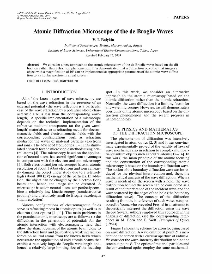
Figure 1 shows the scheme for atom focusing basedon wave diffraction. A wave emitted at point S is inci�dent on the screen with a circular aperture of radius a.We consider the wave�intensity distribution behind thescreen at point P. The optics of material particles andthe conventional optics employ the same mathemati�
PAPERS
Atomic Diffraction Microscope of the de Broglie WavesV. I. Balykin
Institute of Spectroscopy, Troitsk, Moscow region, Russia
Institute of Laser Sciences, University of Electro�Communications, Tokyo, Japan
Received February 15, 2009
Abstract—We consider a new approach to the atomic microscopy of the de Broglie waves based on the dif�fraction rather than refraction phenomenon. It is demonstrated that a diffraction objective that images anobject with a magnification of 103 can be implemented at appropriate parameters of the atomic�wave diffrac�tion by a circular aperture in a real screen.
DOI: 10.1134/S1054660X09180030
48
LASER PHYSICS Vol. 20 No. 1 2010
BALYKIN
cal apparatus. Thus, we analyze the diffraction ofatomic waves using the optical diffraction theory tak�ing into account the corresponding refractive indices(for both photons and atoms). The field�amplitudedistribution at point P at the axis of the system is givenby the Rayleigh integral [15, 16]
(1)
where rs = , rp = , s0 is the dis�tance from the source to the screen, p0 is the distancefrom the screen to the image plane, and ρ is the trans�verse coordinate in the aperture plane.
Using expression (1), we can derive an analyticalexpression for the wave�field distribution [15, 16]:
(2)
where p = + , cosα =
, k = 2π/λ, and λ is the wavelength.
The physical interpretation of result (2) for thewave amplitude behind the screen at point P is as fol�lows. The first term in expression (2) corresponds tothe contribution of the spherical wave emitted by thesource at point S to field�amplitude distribution. Thesecond term describes the contribution of the spheri�cal wave that propagates from source S to the edge ofthe aperture and from the edge of the aperture toobservation point P (this contribution corresponds tothe boundary diffraction wave). The amplitude of thewave scattered by the edge of the aperture is cosα. Theamplitude ratio of the two waves equals
U p( ) p0ikrs( )exp
rs
������������������ 1rp
��� 1∂rp
������ikrs( )exp
rs
������������������⎝ ⎠⎛ ⎞ ρ ρ,d
0
a
∫–=
s02 ρ2
+( )1/2
p02 ρ2
+( )1/2
U p( ) ik s0 p0+( )[ ]/ s0 p0+( )exp=
+ α iπ( ) ikp( )/p,expexpcos
s02
a2
+( )1/2
p02
a2
+( )1/2
p0/ p02
a2
+( )1/2
(3)
If the aperture size satisfies the inequalities a � s0, p0
and a � λ, the contributions of the boundary diffrac�tion wave and the wave incident on the screen can beon the same order of magnitude. It follows fromexpression (2) that the wave intensity at point P isgiven by
(4)
If the source–screen distance is significantly greaterthan the aperture size (s0 � a), expression (4) can berepresented as
(5)
We define the focal point of the diffraction objec�tive as the axial point with the maximum intensity.Then, in accordance with expression (5), the focallength of the diffraction objective is determined fromthe condition cos[k(Δ + Δ0)] = –1. Thus, the lens for�mula of the diffraction objective is written as
(6)
and the focal length is given by
(7)
η 1 a2
2s02
������– a2
2s0p0
����������–⎝ ⎠⎜ ⎟⎛ ⎞
.≅
U2
p( ) = 1
s0 p0+( )2������������������ 1 2 α
s0 p0+p
������������⎝ ⎠⎛ ⎞ k Δ Δ0+( )[ ]coscos–
⎩⎨⎧
+ αs0 p0+( )2
p2
������������������cos2
.
U2
p0( ) 1
s0 p0+( )2������������������ 2 2 Δ Δ0+( )k[ ]cos–{ }.=
1s0
��� 1p0
���+ 1
a2/mλ( )
�����������������, m 1 3 5 …, , ,= =
f a2/mλ.=
Ss0 p0
P
Screen
Boundarywave
2a
ρ
Fig. 1. Schematic drawing that shows image P of point source S resulting from the interference of the incident wave and theboundary diffraction wave in the presence of a screen.
LASER PHYSICS Vol. 20 No. 1 2010
ATOMIC DIFFRACTION MICROSCOPE OF THE DE BROGLIE WAVES 49
Formula (5) shows that an increase in the waveintensity at the axis of the diffraction objective is rep�resented as
(8)
The maximum increase is ξmax = 4.
ξ 2 2 k Δ0 Δ+( )[ ]cos–{ }.=
3. MAIN CHARACTERISTICS
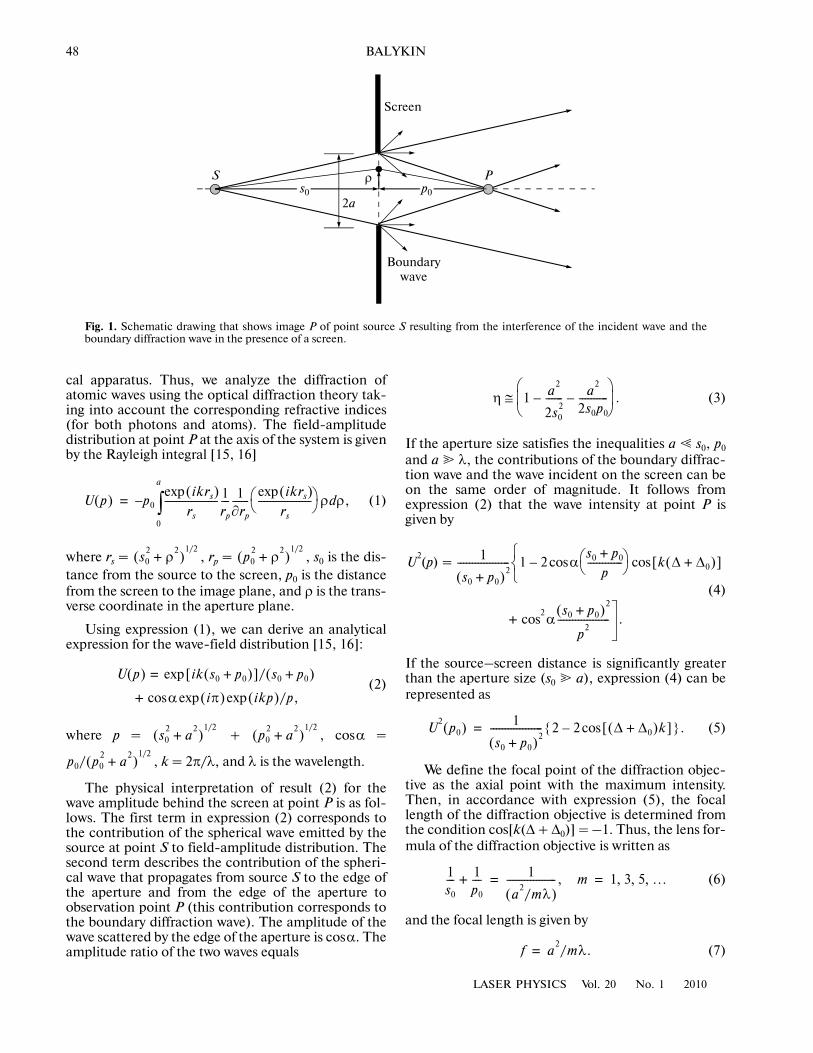
Figure 2 illustrates the focusing by the diffractionobjective. The solid lines in panels (1a)–(3a) show thecurves of the wave intensity at the axis of the diffrac�tion objective versus the distance between the screenand the image plane. The dashed line corresponds tothe wave intensity at the axis in the absence of the
0.5
0
(3a)
z/f1 2
1.0
1.5
2.0
3 4
z0 = f
1
0
(3b)
z/f10 20
2
3
4
30 40
z0 = f
Image distance = ∞
1
0
(2a)
1 2
2
3
3 4
z0 = 2f
1
0
(2b)
1 2
2
3
4
3 4
z0 = 2f
Imag
e d
ista
nce
1
0
(1a)
1 2
2
3
3 4
z0 = ∞
1
0
(1b)
1 2
2
3
4
3 4
z0 = ∞
Imag
e d
ista
nce
Ratio of intensitiesAtom intensity
4
Fig. 2. Plots of (a) the axial intensity of the wave having passed through the diffraction objective and (b) the intensity ratio of thewave at the axis of the diffraction objective and the wave in the absence of the screen vs. the distance from the objective for (1) theinfinite distance between the source and the screen, (2) p0 = 2f, and (3) p0 = f. The dashed lines in panels (a) and (b) show theaxial intensities in the absence of the screen and the positions of the image plane of the diffraction objective, respectively.
50
LASER PHYSICS Vol. 20 No. 1 2010
BALYKIN
screen. Panels (1b)–(3b) demonstrate the ratios of thetwo intensities. The curves are obtained using the datafrom the left�hand panels and illustrate the focusing bythe diffraction objective. In the calculations, weemploy the de Broglie wavelength λB = 0.1 nm and theaperture radius a = 25 nm. The distance from thescreen is measured in the units of the principal focallength f = a2/λ, which is 6.2 μm for the above param�eters. Panels (1a) and (1b) in Fig. 2 correspond to thewave source located at the infinite distance (a planewave is incident on the screen). Panel (1b) shows thewave focusing at the distance z = f in accordance withformula (6).
Panels (2a) and (2b) in Fig. 2 correspond to thesource located at a distance of two focal lengths fromthe screen (s0 = 2f). Formula (6) predicts the maxi�mum wave intensity at the distance z = 2f behind thescreen. The results of the exact calculation based ondiffraction integral (1) (panel (2b) in Fig. 2) providesthe supporting evidence: the intensity maximum cor�responds to two focal lengths. When the source islocated at the distance equal to the focal length (s0 = f)(panels (3a) and (3b) in Fig. 2), the wave behaviorbehind the screen is similar to the wave behavior in asystem with a conventional optical lens: the image ofthe source located at the focal length is formed at aninfinite distance. Note that, in this case, the intensityratio at large distances (p0 > 10f) takes on a constantvalue of 4 (panel (3b) in Fig. 2).
The resolution of the diffraction objective can bestudied using the Fresnel diffraction theory. We con�sider a plane wave incident on the screen with an aper�ture and we search for the transverse wave�amplitudedistribution at the distance equal to the focal length
(panels (3a) and (3b) in Fig. 2). The amplitude distri�bution is determined by the Fresnel diffraction inte�gral [17]:
(9)
where (xf, yf) are the transverse coordinates in the focalplane, k = 2π/λ, and W(x, y) is the amplitude–phasetransparency (APT) at the aperture in the screen.
For the idealized case of the wave diffraction by anaperture in an infinitely thin screen, the APT is
(9.1)
When the aperture is changed by a perfect lens, theAPT is given by
(9.2)
For a real physical aperture in a material screen, theAPT for the de Broglie waves is represented as
(9.3)
where ϕ(x, y) is the phase shift of the wave due to thevan der Waals potential of the screen walls. With allow�ance for the short�range repulsive potential, the vander Waals potential is simulated using the function
(10)
where the first term corresponds to the repulsive sur�face potential and the second term determines theattractive van der Waals potential. Coefficients A, α,and c3 are the characteristic parameters of the poten�tials. We consider the silicon�nitride screen with thethickness h = 50 nm, the aperture radius a = 25 nm,and the metastable He atoms with the de Broglie wave�length λB = 0.1 nm. The parameters of the potentialsare [18] A = 4 × 10¹³ Hz, α = 2 × 10⁹ m–1, and c3 =1.8 × 10–50 J m3.
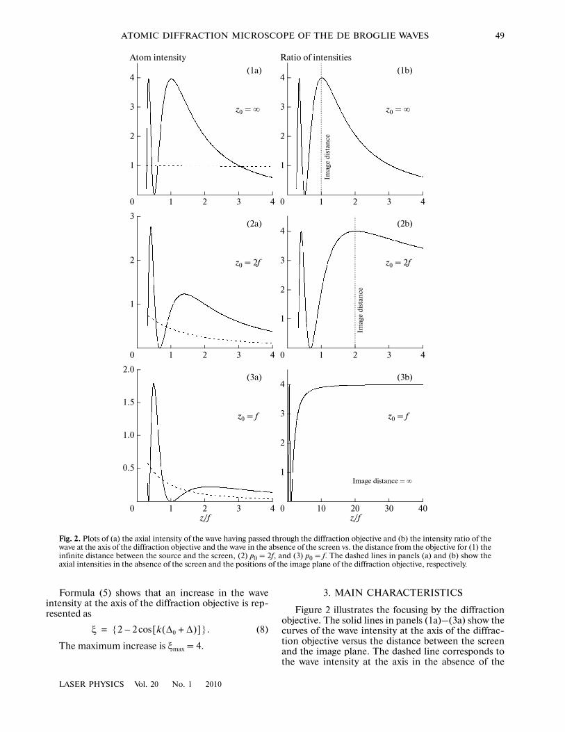
Figure 3 shows the transverse intensity distributionof the de Broglie wave at the focal plane for (a) a per�fect objective whose APT is given by expression (9.2),(b) a perfect diffraction objective whose APT is givenby expression (9.1), and (c) a real diffraction objectivewhose APT is given by expression (9.3). The compari�son shows that the axial intensity of the wave for theperfect objective is greater than the intensities for theperfect and real diffraction objectives by factors of 2and 2.5, respectively. The FWHMs of the distributionsare comparable and are close to the diffraction value,which is ρ = 7 nm for the given configuration. For thereal diffraction objectives, the atoms are partially scat�tered by near�wall potential (10) and this effect con�
U xf yf,( ) 1iλf����� ik
f�� xf
2yf
2+( ) ∫exp=
× W x y,( ) ikf�� xxf yyf+( )–exp xd yd
x y,
∫ ,
W x y,( ) 1.≡
W x y,( ) i k2f��� x
2y
2+( )– .exp=
W x y,( ) iϕ x y,( )–[ ],exp=
V ρ( ) A α a ρ–( )–[ ]exp c3/ a ρ–( )3,–=
2
0
Atom intensity
Transverse coordinate (ρ/a)1 2
4
6
8
10
Ideal atom
Diffraction atom
lens
objective lens
Influence ofvan der Waals
force
Fig. 3. Transverse distributions of the intensity of theatomic de Broglie wave at the focal plane of the diffractionobjective for a perfect objective, a perfect diffraction objec�tive, and a real diffraction objective.
LASER PHYSICS Vol. 20 No. 1 2010
ATOMIC DIFFRACTION MICROSCOPE OF THE DE BROGLIE WAVES 51
tributes to the wings of the distribution. Thus, a realdiffraction objective with the appropriate parameterscan be close to a perfect objective with respect to thefocusing.
4. SCHEME OF THE ATOMIC DIFFRACTION MICROSCOPE
The scheme of the atomic microscope based on thediffraction objective can be similar to the scheme ofthe conventional optical or electron microscope.When an object is located at a distance close to orgreater than the focal length ( f = 6.2 μm), we can eas�ily reach a magnification of 103 at the distance z =0.6 mm from the screen. When the size of an atomicobject equals the minimum spot size in the focal plane(Fig. 3), the image size (7 μm) is comparable with thepixel size of the multichannel plate that is used fordetection of metastable ions (*He and *Ne).
Note that a zone plate (a well�known element invarious types of wave optics) also employs the diffrac�tion for the wave focusing. However, the zone platecan hardly be used for imaging [19], since is representsan aperiodic diffraction grating that concentrates asignificant part of the intensity of the incident wave ina large number of high�order diffraction peaks.
5. CONCLUSIONS
New approach to a problem of the atomic micros�copy based on atomic diffraction rather than theatomic refraction is considered. Diffraction of atomicwave, as a rule, is the fundamental limiting factor ofany wave microscopy. However, as has been shown, onthe basis of this phenomenon and using the lastachievement in nanotechnology, it is possible to createa new type of microscopy of atomic de Broglie waves.
ACKNOWLEDGMENTS
This work was supported in part the Russian Foun�dation for Basic Research (project nos. 08�02�00653a,08�02�00871a, and 09�02�01022a). I am grateful toF. Shimizu, V.S. Letokhov, V.G. Minogin, P.N. Me�lent’ev, and A.E. Afanas’ev for helpful discussions.
REFERENCES
1. V. I. Balykin and V. S. Letokhov, Phys. Today 4, 23(1989).
2. C. S. Adams, M. Sigel, and J. Mlynek, Phys. Rep. 240,141 (1994).
3. P. Meystre, Atom Optics (Springer New York, 2001).4. V. I. Balykin and V. S. Letokhov, Zh. Eksp. Teor. Fiz.
94, 140 (1988); V. I. Balykin and V. S. Letokhov, Opt.Commun. 64, 151 (1987).
5. Appl. Phys. B 54, Spec. Issue Optics and Interferometrywith Atoms, Ed. by J. Mlynek, V. I. Balykin, and P. Mey�stre (1992).
6. J. J. McClelland, R. E. Sholten, E. C. Palm, andR. J. Celotta, Science 262, 877 (1993).
7. V. I. Balykin, V. S. Letokhov, and V. V. Klimov, Pis’maZh. Eksp. Teor. Fiz. 59, 219 (1994) [JETP Lett. 59, 235(1994)].
8. H.�R. Noh, K. Shimizu, and F. Shimizu, Phys. Rev. A61, 041601 (2000).
9. V. I. Balykin, V. S. Letokhov, and V. V. Klimov, Pis’maZh. Eksp. Teor. Fiz. 78, 8 (2003) [JETP Lett. 78, 8(2003)].
10. V. I. Balykin and V. G. Minogin, Phys. Rev. A 77, 01360(2008).
11. D. Kouznetsov, H. Oberst, A. Neumann, Y. Kuznets�ova, K. Shimizu, J.�F. Bisson, K. Ueda, andS. R. J. Brueck, J. Phys. B: At. Mol. Opt. Phys. 39,1605 (2006).
12. D. W. Keith, M. L. Schattenburg, H. I. Smith, andD. E. Pritchard, Phys. Rev. Lett. 61, 1580–1583(1988).
13. O. Carnal and J. Mlynek, Phys. Rev. Lett. 66, 2689(1991).
14. E. M. Rasel, M. K. Oberthaler, H. Batelaan, J. Schmied�mayer, and A. Zeilinger, Phys. Rev. Lett. 75, 2633(1995).
15. C. J. Bouwkamp, Rep. Prog. Phys. 17, 39 (1954).16. H. Osterberg and L. W. Smith, JOSA 51, 1050 (1961).17. J. W. Goodman, Introduction to Fourier Optics
(McGraw�Hill, New York, 1968).18. R. E. Grisenti, W. Schöllkopf, J. P. Toennies,
G. C. Hegerfeldt, and T. Köhler, Phys. Rev. Lett. 83,1755 (1999).
19. M. Bottema, JOSA 59, 1632 (1969).