atom chip for bec interferometry - arxiv · atom chip for bec interferometry 3 surface serves as a...
TRANSCRIPT
RAPID COMMUNICATION
Atom Chip for BEC Interferometry
R J Sewell1‡, J Dingjan1, F Baumgartner1, I Llorente-Garcıa1,
S Eriksson1§, E A Hinds1,G Lewis2, P Srinivasan2, Z Moktadir2,
C O Gollasch2, and M Kraft2
1Centre for Cold Matter, Blackett Laboratory, Imperial College, Prince Consort
Road, London SW7 2BW, United Kingdom2School of Electronics and Computer Science, University of Southampton, Highfield,
Southampton, SO17 1BJ,United Kingdom
E-mail: [email protected]
Abstract. We have fabricated and tested an atom chip that operates as a matter
wave interferometer. In this communication we describe the fabrication of the chip by
ion-beam milling of gold evaporated onto a silicon substrate. We present data on the
quality of the wires, on the current density that can be reached in the wires and on the
smoothness of the magnetic traps that are formed. We demonstrate the operation of
the interferometer, showing that we can coherently split and recombine a BoseEinstein
condensate with good phase stability.
PACS numbers: 03.75.Dg,37.25.+k,81.16.Nd,37.10.Gh
Submitted to: Journal of Physics B: Atomic, Molecular and Optical Physics
‡ Present address: ICFO-Institut de Ciencies Fotoniques, Mediterranean Technology Park, 08860
Castelldefels (Barcelona), Spain.§ Present address: Department of Physics, Swansea University, Singleton Park, Swansea SA2 8PP,
United Kingdom.
arX
iv:0
910.
4547
v2 [
quan
t-ph
] 3
Feb
201
0
Atom Chip for BEC Interferometry 2
Atom chips are microfabricated devices that control electric, magnetic and optical
fields in order to trap and manipulate cold atom clouds and Bose-Einstein condensates
(BECs) [1, 2, 3, 4]. Such devices have significant potential for applications in sensing,
metrology and quantum information processing. Although BEC was first created
on an atom chip 10 years ago [5], the fabrication of functional devices has posed
significant technical challenges that have only recently been overcome. In particular,
BEC interferometry on an atom chip has been demonstrated using static magnetic fields
in combination with radio-frequency [6], optical [7] or microwave fields [8].
In this paper we report on the fabrication and initial testing of a working BEC
interferometer. We have fabricated test batches of atom chips using a variety of
techniques for depositing gold on silicon and for etching the required wire structures.
After evaluating the quality of these we settled on a fabrication method using electron
beam evaporation of a gold layer followed by ion-beam milling to define the wires. We
have used one of the atom chips fabricated in this way to make a BEC interferometer.
5mm
100µm
x
z
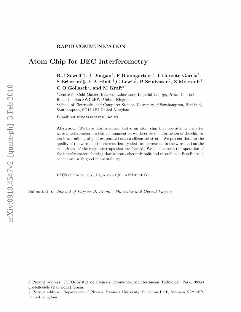
Figure 1. The atom chip used in our interference experiments. Four parallel Z-wires
occupy the central region of the chip and there are two additional end wires. The
surrounding gold pads form a mirror surface used in pre-cooling the atoms in a MOT.
Inset: an optical microscope image of the centre of the chip showing the four parallel
trapping wires (in gold). The silicon substrate can be seen in the gaps between the
wires (in grey). The roughness of the silicon substrate is due to over-etching during
the ion-beam milling.
The atom chip that we have fabricated is shown in figure 1. Four parallel Z-shaped
wires produce the necessary dc and rf fields for trapping and manipulating BECs near
the surface of the chip. The wires in the outer pair are 100µm wide and have a separation
of 300µm (centre-to-centre). The inner wires are 50µm wide with 85µm separation.
The central section of the wires along the z-axis, above which the BEC is produced,
is 7 mm long. Two more wires are patterned onto the chip parallel to the ends of the
Z-wires along the x-axis. These are used to provide additional axial trap depth and to
adjust the field strength at the trap minimum.
In order to load this chip, cold 87Rb atoms from a low-velocity intense source (LVIS)
are first captured 4 mm from the surface in a magneto-optical trap (MOT) [9]. The gold
Atom Chip for BEC Interferometry 3
surface serves as a mirror that reflects some of the laser cooling light, allowing the
MOT to be formed close to the chip. The atoms are then passed to the magnetic trap,
where the cloud is further cooled by forced evaporation using an rf field to eject the
most energetic atoms. A BEC is formed at approximately 500 nK and this provides the
coherent matter wave for our interferometer. The procedure is similar to that described
in our previous publications [10].
Although atom chips are made using standard microfabrication techniques, the
experimental requirements impose a number of unusual design constraints. In order
to create magnetic traps with sufficient depth, the wires must be able to carry several
amperes for a period of ten to twenty seconds. At the same time they should be as
small as possible to manipulate the atoms on a small length scale. This means that
they must be able to carry very large current densities. The wires must also be very
smooth on length scales of up to several hundred microns in order to minimize transverse
currents that lead to roughness of the magnetic trap and fragmentation of cold clouds
(see below). Finally, in order to facilitate pre-cooling of the atoms in a MOT, the entire
chip surface must have a mirror finish.
Gold is our material of choice since it has a low resistivity and high reflectivity at
the relevant laser wavelength. We use a silicon substrate in order to take advantage
of mature fabrication techniques that will allow for future integration of optical
elements such as fibres, cavities, waveguides and pyramid MOTs into a single device
[11, 12, 13, 14]. Silicon has good thermal conductivity, but must be covered in a thin
oxide layer to ensure that the wires are electrically isolated from the substrate.
The wires can be fabricated using standard lithographic techniques or by adapting
thin film hybrid technology [15, 4]. High quality wires have been made by applying
a lift-off technique to an evaporated gold layer [16, 17, 18]. Evaporated gold has
a good surface finish, and the lift-off technique gives the wires good edge definition
when they are thin. However, the method is not well developed for films as thick
as ours. Other groups have patterned a thin gold film photolithographically, then
grown thick wires by electrochemical deposition [19, 20, 21]. Thicker wires can be
fabricated using this technique, but the homogeneity of the gold and definition of
the edges are not as good. In our previous work we have studied techniques for
fabricating gold wires using sputtered and electrochemically deposited gold layers that
are subsequently patterned by wet-etching or ion-beam milling [22]. We have also
investigated growing wires by electrochemical deposition into a mould formed by a
lithographically patterned photoresist [23]. In the light of all these studies, we have
fabricated our BEC interferometer chip using a thick evaporated gold layer patterned
by ion-beam milling.
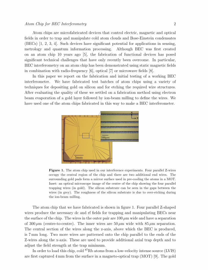
We use a 4 inch p-doped [100] silicon wafer with a resistivity of 17-30 Ωcm to
produce 16 atom chips. The wafer is cleaned using the standard Radio Corporation of
America procedures and fuming nitric acid. It then undergoes wet oxidation to produce
a 100 nm thick oxide layer, the first of several steps illustrated in figure 2. A 40 nm
adhesion layer of chromium is then evaporated over the whole surface, followed by 3µm
Atom Chip for BEC Interferometry 4
SiO2
Au Cr
Si
Photoresist
wet oxidation
evaporation of Cr seed layer
evaporation of Au
spinning of photoresist
reflow of resist
UV photolithography
ion beam milling
plasma ash
Figure 2. Fabrication process flow for electron beam evaporation of a thick gold film
followed by ion-beam milling.
of gold deposited in five steps of 600 nm to avoid overheating the evaporator. After
cleaning in fuming nitric acid, a 2.2µm thick layer of HPR504 photoresist is spun onto
the gold at 500 rpm for 10 seconds, followed by 30 seconds at 1500 rpm. This is given
a soft bake at 90C for 120 seconds, then it is patterned by UV lithography using a
Karl Suss MA8 machine for 9 seconds at 6.5 mW cm−2. Finally, a hard bake is done for
30 min at 140C so that the resist will be easier to remove after it has been subjected
to ion-beam milling. This also causes the resist to develop sloping sides as it reflows a
little.
Milling is done on an IONFAB 300+, with 388 V of beam voltage, 200 mA of current
and 276 V of accelerating voltage. The wafer is cooled to a temperature of 21C using
helium and is milled for 50 minutes, resulting in a maximum cutting depth of 4.4µm.
The resist is quite hard to remove after exposure to the ions, despite the hard bake, so
we use a plasma asher for this purpose run at 110C with 600 W for 60 minutes. Once
all the resist has been removed the wafer is cleaned in fuming nitric acid. The etch rate
is not uniform across the wafer, resulting in over-etching in some places. Where the etch
is too deep, the mill can go through the oxide layer and into the silicon substrate itself.
In that case, re-deposited silicon on the side walls of the cut makes an electrical short
to the wafer. This debris is removed by a 5 second buffered HF acid dip (7:1) followed
by a 5 minute KOH etch. Finally, we use a diamond scriber to cleave the wafer into 16
separate atom chips 24 mm wide and 26 mm long.
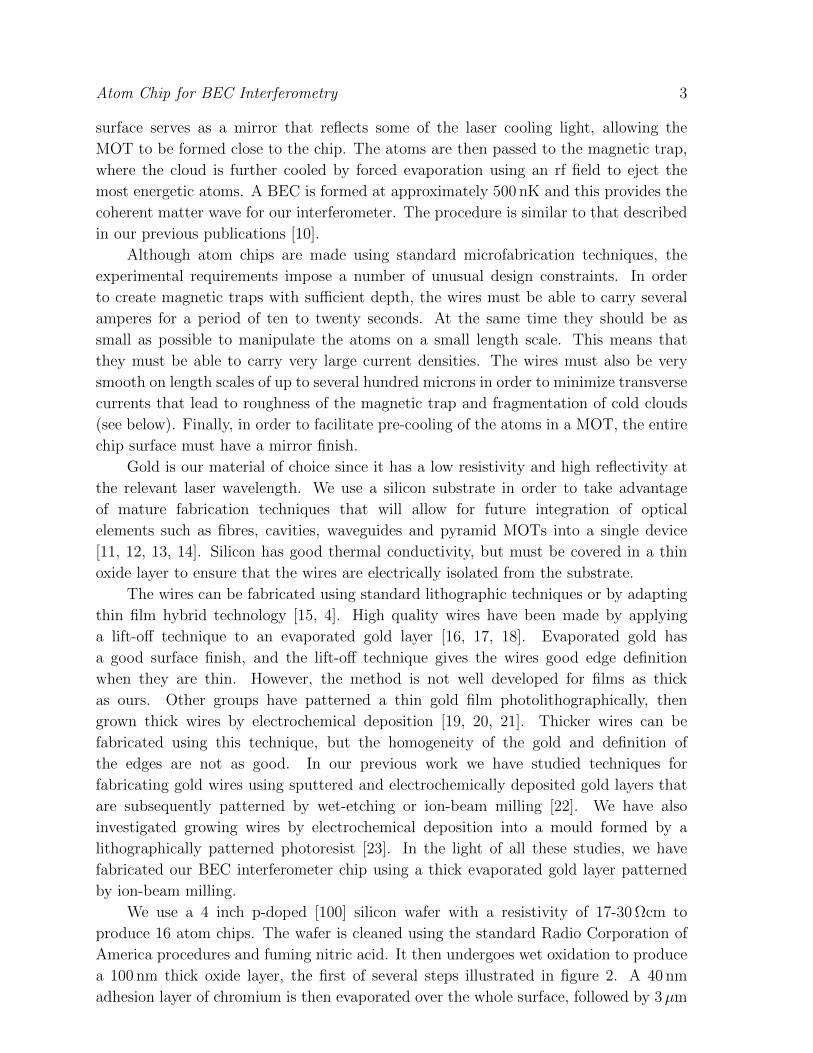
Cleaving a chip through the middle allowed us to examine the cross sectional profiles
of the wires using a scanning electron microscope (SEM). Figure 3(a) shows the sloping
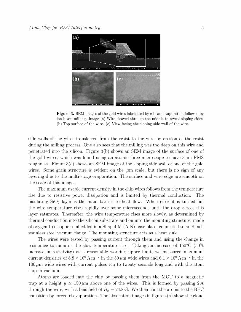
Atom Chip for BEC Interferometry 5
TopSide
(a)
(b) (c)
Figure 3. SEM images of the gold wires fabricated by e-beam evaporation followed by
ion-beam milling. Image (a) Wire cleaved through the middle to reveal sloping sides.
(b) Top surface of the wire. (c) View facing the sloping side wall of the wire.
side walls of the wire, transferred from the resist to the wire by erosion of the resist
during the milling process. One also sees that the milling was too deep on this wire and
penetrated into the silicon. Figure 3(b) shows an SEM image of the surface of one of
the gold wires, which was found using an atomic force microscope to have 3 nm RMS
roughness. Figure 3(c) shows an SEM image of the sloping side wall of one of the gold
wires. Some grain structure is evident on the µm scale, but there is no sign of any
layering due to the multi-stage evaporation. The surface and wire edge are smooth on
the scale of this image.
The maximum usable current density in the chip wires follows from the temperature
rise due to resistive power dissipation and is limited by thermal conduction. The
insulating SiO2 layer is the main barrier to heat flow. When current is turned on,
the wire temperature rises rapidly over some microseconds until the drop across this
layer saturates. Thereafter, the wire temperature rises more slowly, as determined by
thermal conduction into the silicon substrate and on into the mounting structure, made
of oxygen-free copper embedded in a Shapal-M (AlN) base plate, connected to an 8 inch
stainless steel vacuum flange. The mounting structure acts as a heat sink.
The wires were tested by passing current through them and using the change in
resistance to monitor the slow temperature rise. Taking an increase of 150C (50%
increase in resistivity) as a reasonable working upper limit, we measured maximum
current densities of 8.8× 10⁹ A m−2 in the 50µm wide wires and 6.1× 10⁹ A m−2 in the
100µm wide wires with current pulses ten to twenty seconds long and with the atom
chip in vacuum.
Atoms are loaded into the chip by passing them from the MOT to a magnetic
trap at a height y ' 150µm above one of the wires. This is formed by passing 2 A
through the wire, with a bias field of Bx = 24.8 G. We then cool the atoms to the BEC
transition by forced rf evaporation. The absorption images in figure 4(a) show the cloud
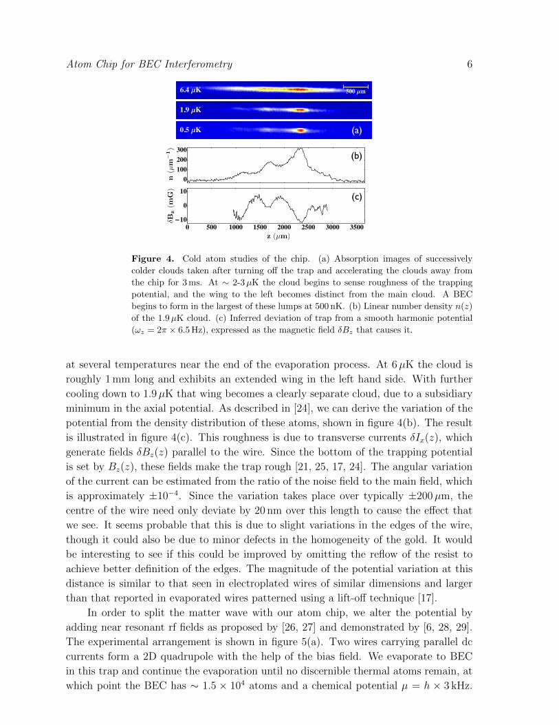
Atom Chip for BEC Interferometry 6
6.4 ΜK
1.9 ΜK
0.5 ΜK
500 Μm
0100200300
(b)
(c)
0 500 1000 1500 2000 2500 3000 350010
0
10
n(µ
m−
1)
δBz
(mG
)
z (µm)
(a)
Figure 4. Cold atom studies of the chip. (a) Absorption images of successively
colder clouds taken after turning off the trap and accelerating the clouds away from
the chip for 3 ms. At ∼ 2-3µK the cloud begins to sense roughness of the trapping
potential, and the wing to the left becomes distinct from the main cloud. A BEC
begins to form in the largest of these lumps at 500 nK. (b) Linear number density n(z)
of the 1.9µK cloud. (c) Inferred deviation of trap from a smooth harmonic potential
(ωz = 2π × 6.5 Hz), expressed as the magnetic field δBz that causes it.
at several temperatures near the end of the evaporation process. At 6µK the cloud is
roughly 1 mm long and exhibits an extended wing in the left hand side. With further
cooling down to 1.9µK that wing becomes a clearly separate cloud, due to a subsidiary
minimum in the axial potential. As described in [24], we can derive the variation of the
potential from the density distribution of these atoms, shown in figure 4(b). The result
is illustrated in figure 4(c). This roughness is due to transverse currents δIx(z), which
generate fields δBz(z) parallel to the wire. Since the bottom of the trapping potential
is set by Bz(z), these fields make the trap rough [21, 25, 17, 24]. The angular variation
of the current can be estimated from the ratio of the noise field to the main field, which
is approximately ±10−4. Since the variation takes place over typically ±200µm, the
centre of the wire need only deviate by 20 nm over this length to cause the effect that
we see. It seems probable that this is due to slight variations in the edges of the wire,
though it could also be due to minor defects in the homogeneity of the gold. It would
be interesting to see if this could be improved by omitting the reflow of the resist to
achieve better definition of the edges. The magnitude of the potential variation at this
distance is similar to that seen in electroplated wires of similar dimensions and larger
than that reported in evaporated wires patterned using a lift-off technique [17].
In order to split the matter wave with our atom chip, we alter the potential by
adding near resonant rf fields as proposed by [26, 27] and demonstrated by [6, 28, 29].
The experimental arrangement is shown in figure 5(a). Two wires carrying parallel dc
currents form a 2D quadrupole with the help of the bias field. We evaporate to BEC
in this trap and continue the evaporation until no discernible thermal atoms remain, at
which point the BEC has ∼ 1.5 × 10⁴ atoms and a chemical potential µ = h × 3 kHz.
Atom Chip for BEC Interferometry 7
0 50 100 150x ΜmN
umberDensitya.u.
(a)
(c)
(b)
(d)
RF Field
DC Trapping Field
External Bias Field
Au wires
Si substrate
DC - RF currentsDC + RF currents
x
y
x
y
x
yΦ 23°
90° Φ 90°Relative Phase Φ
ProbabilityDensity
Figure 5. (a) Configuration of static and rf fields used to split the BEC coherently.
(b) Absorption image of the atomic cloud showing interference fringes formed when the
trapping potential is turned off and the two arms of the BEC interferometer are allowed
to overlap in free fall. (c) The relative phase is obtained by fitting a modulated gaussian
(solid line) to a slice through the centre of the interference pattern. (d) Histogram of
the relative phases extracted from 103 repetitions of the experiment. The solid line is
a fit to the data using a normal distribution. The standard deviation is ∆φ = ±23.
The addition of rf currents, 180 out of phase, generates a near-resonant rf field along
y that splits the cigar-shaped cloud into two parallel clouds. The trap can be smoothly
deformed from a single to a double well by ramping the intensity and/or frequency of
the rf. A typical double well used in our interference experiments has a separation of
∼ 4µm between the two trap minima, and a barrier height of ∼ 10 kHz.
After allowing the two parts to evolve separately for approximately 1 ms, we
read out the relative phase between them by turning off the trapping potential and
allowing them to overlap in free fall. We then take an absorption image of the density
distribution, which exhibits interference fringes perpendicular to the splitting axis, as
illustrated in figure 5(b). We analyse the pattern by fitting a modulated gaussian
n(x) = g(x)(1 + α cos
(2πxΛ
+ φ))
to a slice through the centre, as shown in figure 5(c),
to determine the relative phase φ. In figure 5(d) we plot a histogram of the phases
extracted from 103 repetitions of the experiment. The standard deviation of these is
±23, indicating that the splitting produces a well-defined initial relative phase between
the two arms of the interferometer, as is required for a useful measuring device. This
phase spread is similar to that reported by Schumm et al. [25] for similar experimental
parameters and evolution time.
In conclusion, we have fabricated an atom chip by a process involving electron beam
evaporation of a thick gold layer on a silicon substrate followed by ion-beam milling.
The resulting wires are able to carry high density dc and rf currents and are sufficiently
smooth and uniform to trap a cold atom cloud close to the surface of the chip. We have
used one of these atom chips to make a working BEC interferometer with good phase
Atom Chip for BEC Interferometry 8
stability.
Acknowledgements
The authors acknowledge the expert technical assistance of Jon Dyne. This work was
supported by the UK EPSRC, by the Royal Society, and by the European Commission
through the SCALA and AtomChips networks.
References
[1] Reichel J, Hansel W and Hansch T W 1999 Phys. Rev. Lett. 83 3398–401
[2] Hinds E A and Hughes I G 2002 J. Phys. D 32 R119–46
[3] Folman R, Kruger P, Schmiedmayer J, Denschlag J and Henkel C 2002 Adv. At. Mol. Opt. Phy.
48 263–356
[4] Fortagh J and Zimmermann C 2007 Rev. Mod. Phys. 79 235–89
[5] Hansel W, Hommelhoff P, Hansch T W and Reichel J 2000 Nature 413 498–501
[6] Schumm T, Hofferberth S, Andersson L M, Wildermuth S, Groth S, Bar-Joseph I, Schmiedmayer
J and Kruger P 2005 Nature Physics 1 57–62
[7] Wang Y-J, Anderson D Z, Bright V M, Cornell E A, Diot Q, Kishimoto T, Prentiss M, Saravanan
R A, Segal S and Saijun W 2005 Phys. Rev. Lett. 94 090405
[8] Bohl P, Reidel M F, Hoffrogge J, Reichel J, Hansch T W and Treutlein P 2009 Nat. Phys. 5 592–7
[9] Sinclair C D J, Curtis E A, Llorente Garcıa I, Retter J A, Hall B V, Eriksson S, Sauer B E and
Hinds E A 2005 Phys. Rev. A 72 031603(R)
[10] Jones M P A, Vale C J, Sahagun Sanchez D, Hall B V and Hinds E A 2003 Phys. Rev. Lett. 91
080401
[11] Eriksson S, Trupke M, Powell H F, Sahagun-Sanchez D, Sinclair C D J, Curtis E A, Sauer B E,
Hinds E A, Moktadir Z, Gollasch C O, and Kraft M 2005 Eur. Phys. J. D 35 135–9
[12] Trupke M, Ramirez-Martinez F, Curtis E A, Ashmore J P, Eriksson S, Hinds E A, Moktadir Z,
Gollasch C, Kraft M, Vijaya Prakash G and Baumberg J J 2006 Appl. Phys. Lett. 88 071116
[13] Trupke M, Goldwin J, Darquie B, Dutier G, Eriksson S, Ashmore J P and Hinds E A 2007 Phys.
Rev. Lett. 99 063601
[14] Pollock S, Cotter J P, Laliotis A and Hinds E A 2009 Opt. Express 17 14109–14
[15] Reichel J 2002 Appl. Phys. B 75 469–87
[16] Groth S, Kruger P, Wildermuth S, Folman R, Fernholz T, Schmiedmayer J, Mahalu D and Bar-
Joseph I 2004 Appl. Phys. Lett. 85 2980–2
[17] Kruger P, Andersson L M, Wildermuth S, Hofferberth S, Haller A, Aigner S, Groth S, Bar-Joseph
I and Schmiedmayer J 2007 Phys. Rev. A 76 063621
[18] Trinker M, Groth S, Haslinger S, Manz S, Betz T, Schneider S, Bar-Joseph I, Schumm T and
Schmiedmayer J 2008 Appl. Phys. Lett. 92 254102
[19] Ott H, Fortagh J, Schlotterbeck G, Grossmann A and Zimmermann C 2001 Phys. Rev. Lett. 87
230401
[20] Lev B 2003 Fabrication of micro-magnetic traps for cold neutral atoms, arXiv:quant-ph/0305067v1
[21] Esteve J, Aussibal C, Schumm T, Figl C, Mailly D, Bouchoule I, Westbrook C I and Aspect A
2004 Phys. Rev. A 70 043629
[22] Koukharenko E, Moktadir Z, Kraft M, Abdelsalam M E, Bagnall D M, Vale C, Jones M P A and
Hinds E A 2004 Sens. Actuators, A 115 600–7
[23] Lewis G, Moktadir Z, Gollasch C, Kraft M, Trupke M, Eriksson S and Hinds E A 2005 Proceedings
MME 2005 Conference (Sweden) 56–9
[24] Jones M, Vale C, Sahagun-Sanchez D, Hall B, Eberlein C, Sauer B, Furusawa K, Richardson D
and Hinds E A 2004 J. Phys. B 37 L15–20
Atom Chip for BEC Interferometry 9
[25] Schumm T, Esteve J, Figl C, Trebbia J-B, Aussibal C, Nguyen H, Mailly D, Bouchoule I, Westbrook
C I and Aspect A 2005 Eur. Phys. J. D 32 171–80
[26] Zobay O and Garraway B 2001 Phys. Rev. Lett. 86 1195–8
[27] Zobay O and Garraway B 2004 Phys. Rev. A 69 023605
[28] Colombe Y, Knyazchyan E, Morizot O, Mercier B, Lorent V and Perrin H 2007 Europhys. Lett.
67 593–9
[29] Jo G-B, Shin Y, Will S, Pasquini T A, Saba M, Ketterle W, Pritchard D E, Vengalattore M and
Prentiss M 2007 Phys. Rev. Lett. 98 030407