atmega2560 summary
DESCRIPTION
Atmega2560 SummaryTRANSCRIPT
8-bit Atmel Microcontroller with 64K/128K/256K Bytes In-SystemProgrammable Flash
ATmega640/VATmega1280/VATmega1281/VATmega2560/VATmega2561/V
Summary
2549PS–AVR–10/2012
Features• High Performance, Low Power Atmel® AVR® 8-Bit Microcontroller• Advanced RISC Architecture
– 135 Powerful Instructions – Most Single Clock Cycle Execution– 32 × 8 General Purpose Working Registers– Fully Static Operation– Up to 16 MIPS Throughput at 16MHz– On-Chip 2-cycle Multiplier
• High Endurance Non-volatile Memory Segments– 64K/128K/256KBytes of In-System Self-Programmable Flash – 4Kbytes EEPROM– 8Kbytes Internal SRAM– Write/Erase Cycles:10,000 Flash/100,000 EEPROM– Data retention: 20 years at 85°C/ 100 years at 25°C– Optional Boot Code Section with Independent Lock Bits
• In-System Programming by On-chip Boot Program• True Read-While-Write Operation
– Programming Lock for Software Security• Endurance: Up to 64Kbytes Optional External Memory Space
• Atmel® QTouch® library support– Capacitive touch buttons, sliders and wheels– QTouch and QMatrix® acquisition– Up to 64 sense channels
• JTAG (IEEE std. 1149.1 compliant) Interface– Boundary-scan Capabilities According to the JTAG Standard– Extensive On-chip Debug Support– Programming of Flash, EEPROM, Fuses, and Lock Bits through the JTAG Interface
• Peripheral Features– Two 8-bit Timer/Counters with Separate Prescaler and Compare Mode– Four 16-bit Timer/Counter with Separate Prescaler, Compare- and Capture Mode– Real Time Counter with Separate Oscillator– Four 8-bit PWM Channels– Six/Twelve PWM Channels with Programmable Resolution from 2 to 16 Bits
(ATmega1281/2561, ATmega640/1280/2560)– Output Compare Modulator– 8/16-channel, 10-bit ADC (ATmega1281/2561, ATmega640/1280/2560)– Two/Four Programmable Serial USART (ATmega1281/2561, ATmega640/1280/2560)– Master/Slave SPI Serial Interface– Byte Oriented 2-wire Serial Interface– Programmable Watchdog Timer with Separate On-chip Oscillator– On-chip Analog Comparator– Interrupt and Wake-up on Pin Change
• Special Microcontroller Features– Power-on Reset and Programmable Brown-out Detection– Internal Calibrated Oscillator– External and Internal Interrupt Sources– Six Sleep Modes: Idle, ADC Noise Reduction, Power-save, Power-down, Standby,
and Extended Standby• I/O and Packages
– 54/86 Programmable I/O Lines (ATmega1281/2561, ATmega640/1280/2560)– 64-pad QFN/MLF, 64-lead TQFP (ATmega1281/2561)– 100-lead TQFP, 100-ball CBGA (ATmega640/1280/2560)– RoHS/Fully Green
• Temperature Range:– -40°C to 85°C Industrial
• Ultra-Low Power Consumption– Active Mode: 1MHz, 1.8V: 500µA– Power-down Mode: 0.1µA at 1.8V
• Speed Grade:– ATmega640V/ATmega1280V/ATmega1281V:
• 0 - 4MHz @ 1.8V - 5.5V, 0 - 8MHz @ 2.7V - 5.5V– ATmega2560V/ATmega2561V:
• 0 - 2MHz @ 1.8V - 5.5V, 0 - 8MHz @ 2.7V - 5.5V– ATmega640/ATmega1280/ATmega1281:
• 0 - 8MHz @ 2.7V - 5.5V, 0 - 16MHz @ 4.5V - 5.5V– ATmega2560/ATmega2561:
• 0 - 16MHz @ 4.5V - 5.5V
ATmega640/1280/1281/2560/2561
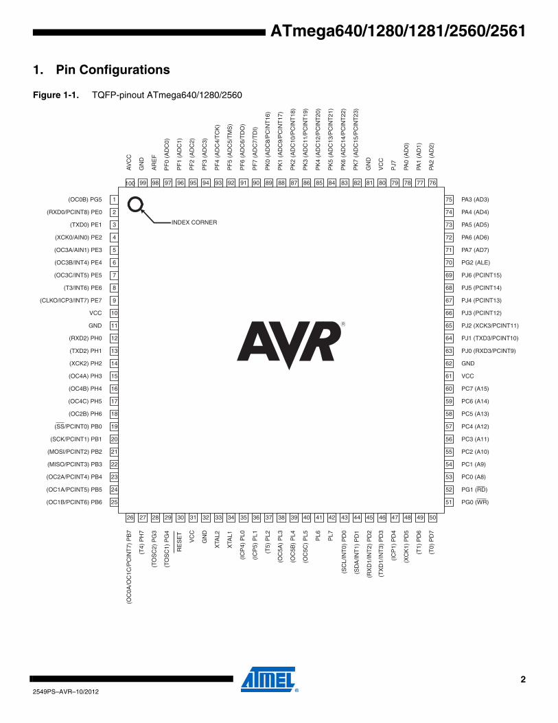
1. Pin Configurations
Figure 1-1. TQFP-pinout ATmega640/1280/2560
GN
D
VC
C
PA0
(AD
0)
PA1
(AD
1)
PA2
(AD
2)
PA3 (AD3)
PA4 (AD4)
PA5 (AD5)
PA6 (AD6)
PA7 (AD7)
PG2 (ALE)
AV
CC
GN
D
AR
EF
PF
0 (A
DC
0)
PF
1 (A
DC
1)
PF
2 (A
DC
2)
PF
3 (A
DC
3)
PF
4 (A
DC
4/T
CK
)
PF
5 (A
DC
5/T
MS
)
PF
6 (A
DC
6/T
DO
)
PF
7 (A
DC
7/T
DI)
100 99 98 97 96 95 94 93 92 91 90 89 88 87 86 85 84 83 82 81 80 79 78 77 76
1
2
3
4
5
6
7
8
9
10
11
12
13
14
15
16
17
18
19
20
21
22
23
24
25
75
74
73
72
71
70
69
68
67
66
65
64
63
62
61
60
59
58
57
56
55
54
53
52
51
26 28 29 3127 3630 32 35 3733 34 38 39 40 41 42 43 44 45 46 47 48 49 50
PK
0 (A
DC
8/P
CIN
T16
)
PK
1 (A
DC
9/P
CIN
T17
)
PK
2 (A
DC
10/P
CIN
T18
)
PK
3 (A
DC
11/P
CIN
T19
)
PK
4 (A
DC
12/P
CIN
T20
)
PK
5 (A
DC
13/P
CIN
T21
)
PK
6 (A
DC
14/P
CIN
T22
)
PK
7 (A
DC
15/P
CIN
T23
)
(OC2B) PH6
(TO
SC
2) P
G3
(TO
SC
1) P
G4
RE
SE
T
(T4)
PH
7
(IC
P4)
PL0
VC
C
GN
D
XTA
L2
XTA
L1
PL6
PL7
GND
VCC
(OC0B) PG5
VCC
GND
(RXD2) PH0
(TXD2) PH1
(XCK2) PH2
(OC4A) PH3
(OC4B) PH4
(OC4C) PH5
(RXD0/PCINT8) PE0
(TXD0) PE1
(XCK0/AIN0) PE2
(OC3A/AIN1) PE3
(OC3B/INT4) PE4
(OC3C/INT5) PE5
(T3/INT6) PE6
(CLKO/ICP3/INT7) PE7
(SS/PCINT0) PB0
(SCK/PCINT1) PB1
(MOSI/PCINT2) PB2
(MISO/PCINT3) PB3
(OC2A/PCINT4) PB4
(OC1A/PCINT5) PB5
(OC1B/PCINT6) PB6
(OC
0A/O
C1C
/PC
INT
7) P
B7
PC7 (A15)
PC6 (A14)
PC5 (A13)
PC4 (A12)
PC3 (A11)
PC2 (A10)
PC1 (A9)
PC0 (A8)
PG1 (RD)
PG0 (WR)
(TX
D1/
INT
3) P
D3
(IC
P1)
PD
4
(XC
K1)
PD
5
(T1)
PD
6
(T0)
PD
7
(SC
L/IN
T0)
PD
0
(SD
A/IN
T1)
PD
1
(RX
D1/
INT
2) P
D2
(IC
P5)
PL1
(T5)
PL2
(OC
5A)
PL3
(OC
5B)
PL4
PJ6 (PCINT15)
PJ5 (PCINT14)
PJ4 (PCINT13)
PJ3 (PCINT12)
PJ2 (XCK3/PCINT11)
PJ1 (TXD3/PCINT10)
PJ0 (RXD3/PCINT9)
PJ7
(OC
5C)
PL5
INDEX CORNER
22549PS–AVR–10/2012
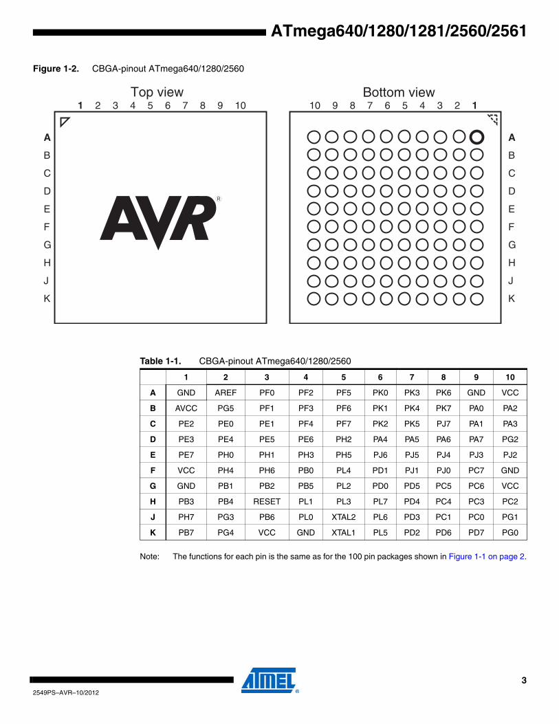
ATmega640/1280/1281/2560/2561
Figure 1-2. CBGA-pinout ATmega640/1280/2560
Note: The functions for each pin is the same as for the 100 pin packages shown in Figure 1-1 on page 2.
A
B
C
D
E
F
G
H
J
K
1 2 3 4 5 6 7 8 9 10
A
B
C
D
E
F
G
H
J
K
10 9 8 7 6 5 4 3 2 1Top view Bottom view
Table 1-1. CBGA-pinout ATmega640/1280/2560
1 2 3 4 5 6 7 8 9 10
A GND AREF PF0 PF2 PF5 PK0 PK3 PK6 GND VCC
B AVCC PG5 PF1 PF3 PF6 PK1 PK4 PK7 PA0 PA2
C PE2 PE0 PE1 PF4 PF7 PK2 PK5 PJ7 PA1 PA3
D PE3 PE4 PE5 PE6 PH2 PA4 PA5 PA6 PA7 PG2
E PE7 PH0 PH1 PH3 PH5 PJ6 PJ5 PJ4 PJ3 PJ2
F VCC PH4 PH6 PB0 PL4 PD1 PJ1 PJ0 PC7 GND
G GND PB1 PB2 PB5 PL2 PD0 PD5 PC5 PC6 VCC
H PB3 PB4 RESET PL1 PL3 PL7 PD4 PC4 PC3 PC2
J PH7 PG3 PB6 PL0 XTAL2 PL6 PD3 PC1 PC0 PG1
K PB7 PG4 VCC GND XTAL1 PL5 PD2 PD6 PD7 PG0
32549PS–AVR–10/2012
ATmega640/1280/1281/2560/2561
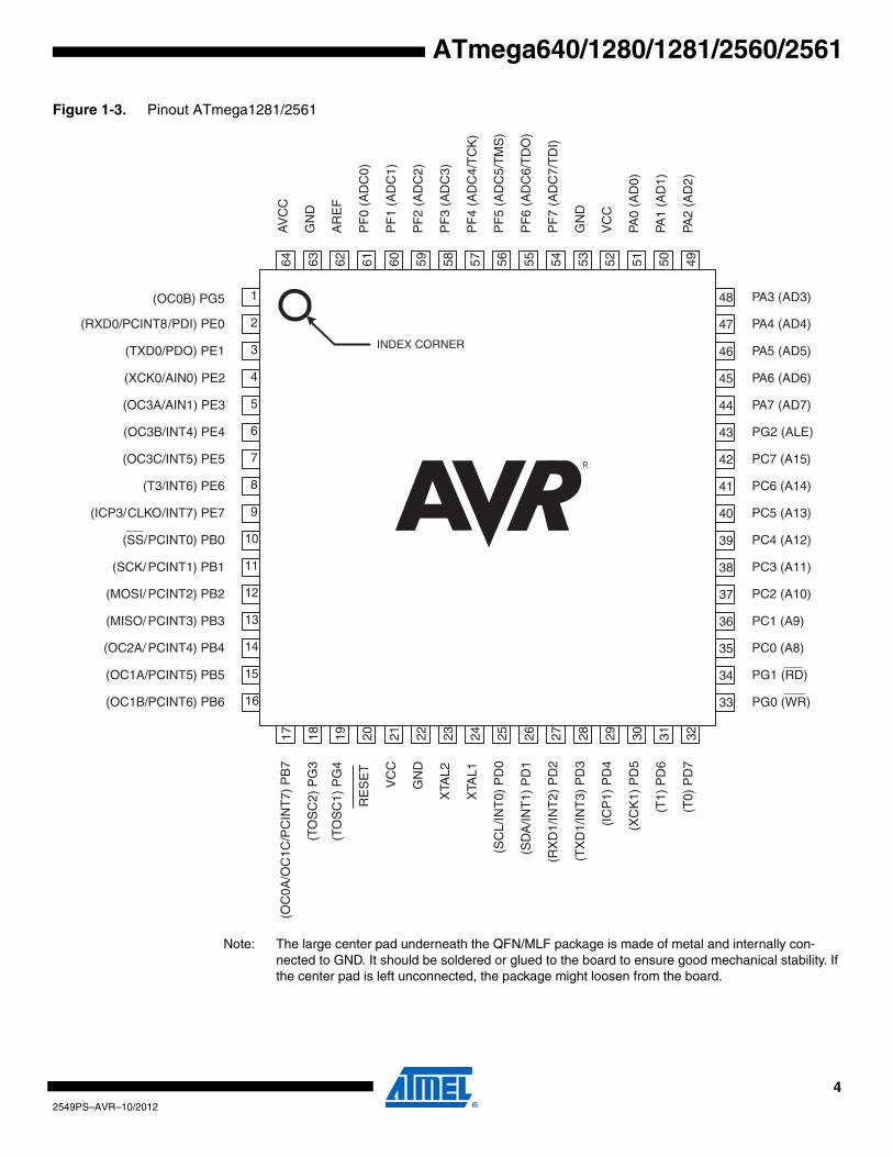
Figure 1-3. Pinout ATmega1281/2561
Note: The large center pad underneath the QFN/MLF package is made of metal and internally con-nected to GND. It should be soldered or glued to the board to ensure good mechanical stability. If the center pad is left unconnected, the package might loosen from the board.
(RXD0/PCINT8/PDI) PE0
(TXD0/PDO) PE1
(XCK0/AIN0) PE2
(OC3A/AIN1) PE3
(OC3B/INT4) PE4
(OC3C/INT5) PE5
(T3/INT6) PE6
(ICP3/CLKO/INT7) PE7
(SS/PCINT0) PB0
(OC0B) PG5
(SCK/PCINT1) PB1
(MOSI/PCINT2) PB2
(MISO/PCINT3) PB3
(OC2A/ PCINT4) PB4
(OC1A/PCINT5) PB5
(OC1B/PCINT6) PB6
(OC
0A/O
C1C
/PC
INT
7) P
B7
(TO
SC
2) P
G3
(TO
SC
1) P
G4
RE
SE
T
VC
C
GN
D
XTA
L2
XTA
L1
(SC
L/IN
T0)
PD
0
(SD
A/IN
T1)
PD
1
(RX
D1/
INT
2) P
D2
(TX
D1/
INT
3) P
D3
(IC
P1)
PD
4
(XC
K1)
PD
5
PA3 (AD3)
PA4 (AD4)
PA5 (AD5)
PA6 (AD6)
PA7 (AD7)
PG2 (ALE)
PC7 (A15)
PC6 (A14)
PC5 (A13)
PC4 (A12)
PC3 (A11)
PC2 (A10)
PC1 (A9)
PC0 (A8)
PG1 (RD)
PG0 (WR)
AV
CC
GN
D
AR
EF
PF
0 (A
DC
0)
PF
1 (A
DC
1)
PF
2 (A
DC
2)
PF
3 (A
DC
3)
PF
4 (A
DC
4/T
CK
)
PF
5 (A
DC
5/T
MS
)
PF
6 (A
DC
6/T
DO
)
PF
7 (A
DC
7/T
DI)
GN
D
VC
C
PA0
(AD
0)
PA1
(AD
1)
PA2
(AD
2)
(T1)
PD
6
(T0)
PD
7
INDEX CORNER
1
2
3
4
5
6
7
8
9
10
11
12
13
14
15
16
64 63 62 61 60 59 58 57 56 55 54 53 52 51 50 49
48
47
46
45
44
43
42
41
40
39
38
37
36
35
34
33
17 18 19 20 21 22 23 24 25 26 27 28 29 30 31 32
42549PS–AVR–10/2012
ATmega640/1280/1281/2560/2561
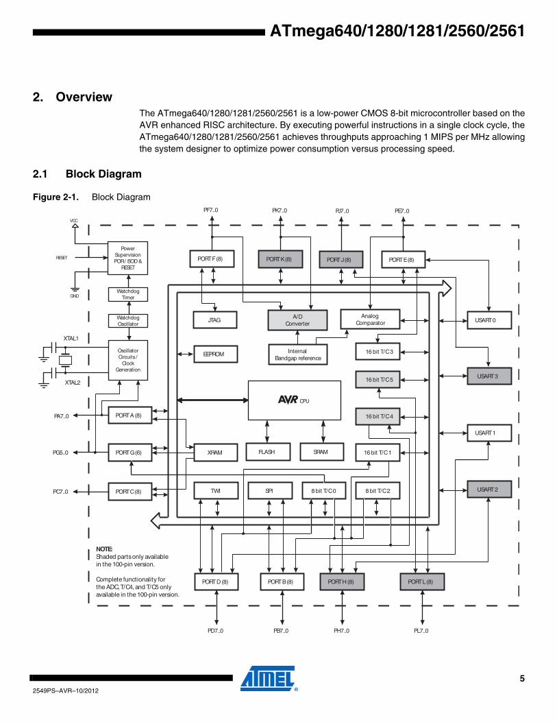
2. OverviewThe ATmega640/1280/1281/2560/2561 is a low-power CMOS 8-bit microcontroller based on theAVR enhanced RISC architecture. By executing powerful instructions in a single clock cycle, theATmega640/1280/1281/2560/2561 achieves throughputs approaching 1 MIPS per MHz allowingthe system designer to optimize power consumption versus processing speed.
2.1 Block Diagram
Figure 2-1. Block Diagram
CPU
GND
VCC
RESET
PowerSupervisionPOR / BOD &
RESET
WatchdogOscillator
WatchdogTimer
OscillatorCircuits /
ClockGeneration
XTAL1
XTAL2
PC7..0 PORT C (8)
PA7..0 PORT A (8)
PORT D (8)
PD7..0
PORT B (8)
PB7..0
PORT E (8)
PE7..0
PORT F (8)
PF7..0
PORT J (8)
PJ7..0
PG5..0 PORT G (6)
PORT H (8)
PH7..0
PORT K (8)
PK7..0
PORT L (8)
PL7..0
XRAM
TWI SPI
EEPROM
JTAG
8 bit T/C 0 8 bit T/C 2
16 bit T/C 1
16 bit T/C 3
SRAMFLASH
16 bit T/C 4
16 bit T/C 5
USART 2
USART 1
USART 0
Internal Bandgap reference
Analog Comparator
A/DConverter
USART 3
NOTE:Shaded parts only availablein the 100-pin version.
Complete functionality forthe ADC, T/C4, and T/C5 only available in the 100-pin version.
52549PS–AVR–10/2012
ATmega640/1280/1281/2560/2561
The Atmel® AVR® core combines a rich instruction set with 32 general purpose working regis-ters. All the 32 registers are directly connected to the Arithmetic Logic Unit (ALU), allowing twoindependent registers to be accessed in one single instruction executed in one clock cycle. Theresulting architecture is more code efficient while achieving throughputs up to ten times fasterthan conventional CISC microcontrollers.
The ATmega640/1280/1281/2560/2561 provides the following features: 64K/128K/256K bytes ofIn-System Programmable Flash with Read-While-Write capabilities, 4Kbytes EEPROM, 8Kbytes SRAM, 54/86 general purpose I/O lines, 32 general purpose working registers, RealTime Counter (RTC), six flexible Timer/Counters with compare modes and PWM, 4 USARTs, abyte oriented 2-wire Serial Interface, a 16-channel, 10-bit ADC with optional differential inputstage with programmable gain, programmable Watchdog Timer with Internal Oscillator, an SPIserial port, IEEE® std. 1149.1 compliant JTAG test interface, also used for accessing the On-chip Debug system and programming and six software selectable power saving modes. The Idlemode stops the CPU while allowing the SRAM, Timer/Counters, SPI port, and interrupt systemto continue functioning. The Power-down mode saves the register contents but freezes theOscillator, disabling all other chip functions until the next interrupt or Hardware Reset. In Power-save mode, the asynchronous timer continues to run, allowing the user to maintain a timer basewhile the rest of the device is sleeping. The ADC Noise Reduction mode stops the CPU and allI/O modules except Asynchronous Timer and ADC, to minimize switching noise during ADCconversions. In Standby mode, the Crystal/Resonator Oscillator is running while the rest of thedevice is sleeping. This allows very fast start-up combined with low power consumption. InExtended Standby mode, both the main Oscillator and the Asynchronous Timer continue to run.
Atmel offers the QTouch® library for embedding capacitive touch buttons, sliders and wheels-functionality into AVR microcontrollers. The patented charge-transfer signal acquisitionoffersrobust sensing and includes fully debounced reporting of touch keys and includes AdjacentKeySuppression® (AKS™) technology for unambiguous detection of key events. The easy-to-useQTouch Suite toolchain allows you to explore, develop and debug your own touch applications.
The device is manufactured using Atmel’s high-density nonvolatile memory technology. The On-chip ISP Flash allows the program memory to be reprogrammed in-system through an SPI serialinterface, by a conventional nonvolatile memory programmer, or by an On-chip Boot programrunning on the AVR core. The boot program can use any interface to download the applicationprogram in the application Flash memory. Software in the Boot Flash section will continue to runwhile the Application Flash section is updated, providing true Read-While-Write operation. Bycombining an 8-bit RISC CPU with In-System Self-Programmable Flash on a monolithic chip,the Atmel ATmega640/1280/1281/2560/2561 is a powerful microcontroller that provides a highlyflexible and cost effective solution to many embedded control applications.
The ATmega640/1280/1281/2560/2561 AVR is supported with a full suite of program and sys-tem deve lopment too ls inc lud ing : C compi le rs , macro assemb le rs , p rog ramdebugger/simulators, in-circuit emulators, and evaluation kits.
62549PS–AVR–10/2012
ATmega640/1280/1281/2560/2561
2.2 Comparison Between ATmega1281/2561 and ATmega640/1280/2560Each device in the ATmega640/1280/1281/2560/2561 family differs only in memory size andnumber of pins. Table 2-1 summarizes the different configurations for the six devices.
2.3 Pin Descriptions
2.3.1 VCCDigital supply voltage.
2.3.2 GNDGround.
2.3.3 Port A (PA7..PA0)Port A is an 8-bit bi-directional I/O port with internal pull-up resistors (selected for each bit). ThePort A output buffers have symmetrical drive characteristics with both high sink and sourcecapability. As inputs, Port A pins that are externally pulled low will source current if the pull-upresistors are activated. The Port A pins are tri-stated when a reset condition becomes active,even if the clock is not running.
Por t A a lso se rves the func t ions o f va r ious spec ia l fea tu res o f theATmega640/1280/1281/2560/2561 as listed on page 78.
2.3.4 Port B (PB7..PB0)Port B is an 8-bit bi-directional I/O port with internal pull-up resistors (selected for each bit). ThePort B output buffers have symmetrical drive characteristics with both high sink and sourcecapability. As inputs, Port B pins that are externally pulled low will source current if the pull-upresistors are activated. The Port B pins are tri-stated when a reset condition becomes active,even if the clock is not running.
Port B has better driving capabilities than the other ports.
Por t B a lso se rves the func t ions o f va r ious spec ia l fea tu res o f theATmega640/1280/1281/2560/2561 as listed on page 79.
2.3.5 Port C (PC7..PC0)Port C is an 8-bit bi-directional I/O port with internal pull-up resistors (selected for each bit). ThePort C output buffers have symmetrical drive characteristics with both high sink and sourcecapability. As inputs, Port C pins that are externally pulled low will source current if the pull-up
Table 2-1. Configuration Summary
Device Flash EEPROM RAMGeneral
Purpose I/O pins16 bits resolution
PWM channelsSerial
USARTsADC
Channels
ATmega640 64KB 4KB 8KB 86 12 4 16
ATmega1280 128KB 4KB 8KB 86 12 4 16
ATmega1281 128KB 4KB 8KB 54 6 2 8
ATmega2560 256KB 4KB 8KB 86 12 4 16
ATmega2561 256KB 4KB 8KB 54 6 2 8
72549PS–AVR–10/2012
ATmega640/1280/1281/2560/2561
resistors are activated. The Port C pins are tri-stated when a reset condition becomes active,even if the clock is not running.
Port C also serves the functions of special features of the ATmega640/1280/1281/2560/2561 aslisted on page 82.
2.3.6 Port D (PD7..PD0)Port D is an 8-bit bi-directional I/O port with internal pull-up resistors (selected for each bit). ThePort D output buffers have symmetrical drive characteristics with both high sink and sourcecapability. As inputs, Port D pins that are externally pulled low will source current if the pull-upresistors are activated. The Port D pins are tri-stated when a reset condition becomes active,even if the clock is not running.
Por t D a lso se rves the func t ions o f va r ious spec ia l fea tu res o f theATmega640/1280/1281/2560/2561 as listed on page 83.
2.3.7 Port E (PE7..PE0)Port E is an 8-bit bi-directional I/O port with internal pull-up resistors (selected for each bit). ThePort E output buffers have symmetrical drive characteristics with both high sink and sourcecapability. As inputs, Port E pins that are externally pulled low will source current if the pull-upresistors are activated. The Port E pins are tri-stated when a reset condition becomes active,even if the clock is not running.
Por t E a lso se rves the func t ions o f va r ious spec ia l fea tu res o f theATmega640/1280/1281/2560/2561 as listed on page 86.
2.3.8 Port F (PF7..PF0)Port F serves as analog inputs to the A/D Converter.
Port F also serves as an 8-bit bi-directional I/O port, if the A/D Converter is not used. Port pinscan provide internal pull-up resistors (selected for each bit). The Port F output buffers have sym-metrical drive characteristics with both high sink and source capability. As inputs, Port F pinsthat are externally pulled low will source current if the pull-up resistors are activated. The Port Fpins are tri-stated when a reset condition becomes active, even if the clock is not running. If theJTAG interface is enabled, the pull-up resistors on pins PF7(TDI), PF5(TMS), and PF4(TCK) willbe activated even if a reset occurs.
Port F also serves the functions of the JTAG interface.
2.3.9 Port G (PG5..PG0)Port G is a 6-bit I/O port with internal pull-up resistors (selected for each bit). The Port G outputbuffers have symmetrical drive characteristics with both high sink and source capability. Asinputs, Port G pins that are externally pulled low will source current if the pull-up resistors areactivated. The Port G pins are tri-stated when a reset condition becomes active, even if the clockis not running.
Por t G a lso se rves the func t ions o f va r ious spec ia l f ea tu res o f theATmega640/1280/1281/2560/2561 as listed on page 90.
2.3.10 Port H (PH7..PH0)Port H is a 8-bit bi-directional I/O port with internal pull-up resistors (selected for each bit). ThePort H output buffers have symmetrical drive characteristics with both high sink and sourcecapability. As inputs, Port H pins that are externally pulled low will source current if the pull-up
82549PS–AVR–10/2012
ATmega640/1280/1281/2560/2561
resistors are activated. The Port H pins are tri-stated when a reset condition becomes active,even if the clock is not running.
Port H also serves the functions of various special features of the ATmega640/1280/2560 aslisted on page 92.
2.3.11 Port J (PJ7..PJ0)Port J is a 8-bit bi-directional I/O port with internal pull-up resistors (selected for each bit). ThePort J output buffers have symmetrical drive characteristics with both high sink and source capa-bility. As inputs, Port J pins that are externally pulled low will source current if the pull-upresistors are activated. The Port J pins are tri-stated when a reset condition becomes active,even if the clock is not running.
Port J also serves the functions of various special features of the ATmega640/1280/2560 aslisted on page 94.
2.3.12 Port K (PK7..PK0)Port K serves as analog inputs to the A/D Converter.
Port K is a 8-bit bi-directional I/O port with internal pull-up resistors (selected for each bit). ThePort K output buffers have symmetrical drive characteristics with both high sink and sourcecapability. As inputs, Port K pins that are externally pulled low will source current if the pull-upresistors are activated. The Port K pins are tri-stated when a reset condition becomes active,even if the clock is not running.
Port K also serves the functions of various special features of the ATmega640/1280/2560 aslisted on page 96.
2.3.13 Port L (PL7..PL0)Port L is a 8-bit bi-directional I/O port with internal pull-up resistors (selected for each bit). ThePort L output buffers have symmetrical drive characteristics with both high sink and sourcecapability. As inputs, Port L pins that are externally pulled low will source current if the pull-upresistors are activated. The Port L pins are tri-stated when a reset condition becomes active,even if the clock is not running.
Port L also serves the functions of various special features of the ATmega640/1280/2560 aslisted on page 98.
2.3.14 RESETReset input. A low level on this pin for longer than the minimum pulse length will generate areset, even if the clock is not running. The minimum pulse length is given in “System and ResetCharacteristics” on page 372. Shorter pulses are not guaranteed to generate a reset.
2.3.15 XTAL1Input to the inverting Oscillator amplifier and input to the internal clock operating circuit.
2.3.16 XTAL2Output from the inverting Oscillator amplifier.
92549PS–AVR–10/2012
ATmega640/1280/1281/2560/2561
2.3.17 AVCCAVCC is the supply voltage pin for Port F and the A/D Converter. It should be externally con-nected to VCC, even if the ADC is not used. If the ADC is used, it should be connected to VCC
through a low-pass filter.
2.3.18 AREFThis is the analog reference pin for the A/D Converter.
102549PS–AVR–10/2012
ATmega640/1280/1281/2560/2561
3. ResourcesA comprehensive set of development tools and application notes, and datasheets are availablefor download on http://www.atmel.com/avr.
4. About Code ExamplesThis documentation contains simple code examples that briefly show how to use various parts ofthe device. Be aware that not all C compiler vendors include bit definitions in the header filesand interrupt handling in C is compiler dependent. Please confirm with the C compiler documen-tation for more details.
These code examples assume that the part specific header file is included before compilation.For I/O registers located in extended I/O map, "IN", "OUT", "SBIS", "SBIC", "CBI", and "SBI"instructions must be replaced with instructions that allow access to extended I/O. Typically"LDS" and "STS" combined with "SBRS", "SBRC", "SBR", and "CBR".
5. Data RetentionReliability Qualification results show that the projected data retention failure rate is much lessthan 1 ppm over 20 years at 85°C or 100 years at 25°C.
6. Capacitive touch sensingThe Atmel®QTouch® Library provides a simple to use solution to realize touch sensitive inter-faces on most Atmel AVR® microcontrollers. The QTouch Library includes support for theQTouch and QMatrix® acquisition methods.
Touch sensing can be added to any application by linking the appropriate Atmel QTouch Libraryfor the AVR Microcontroller. This is done by using a simple set of APIs to define the touch chan-nels and sensors, and then calling the touch sensing API’s to retrieve the channel informationand determine the touch sensor states.
The QTouch Library is FREE and downloadable from the Atmel website at the following location:www.atmel.com/qtouchlibrary. For implementation details and other information, refer to theAtmel QTouch Library User Guide - also available for download from the Atmel website.
112549PS–AVR–10/2012
ATmega640/1280/1281/2560/2561
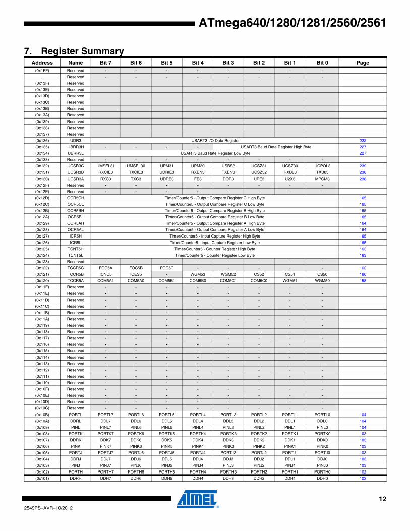
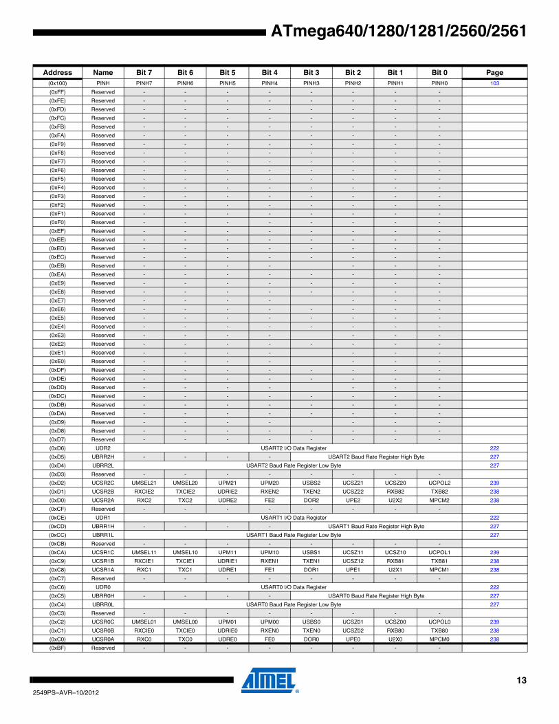
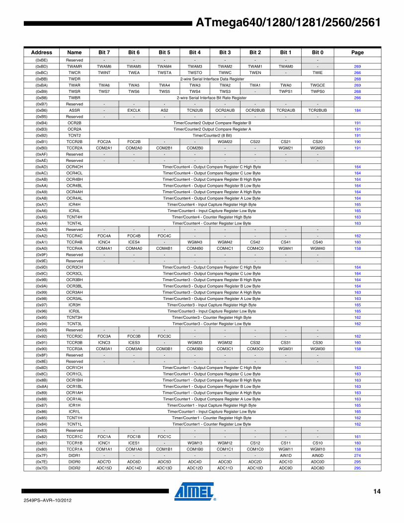
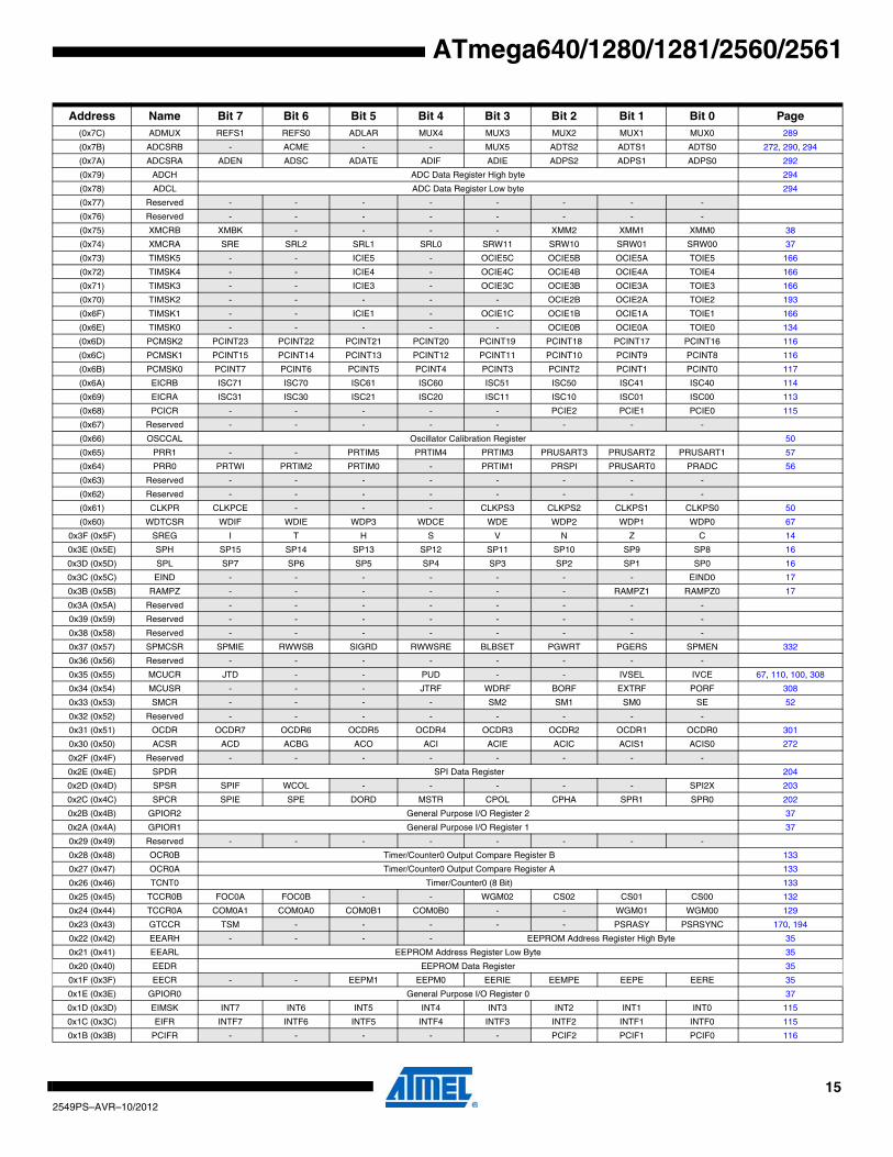
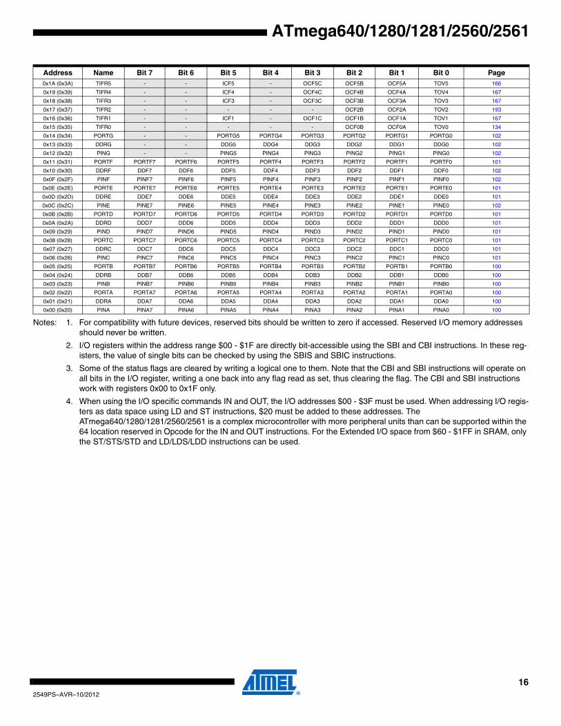
7. Register SummaryAddress Name Bit 7 Bit 6 Bit 5 Bit 4 Bit 3 Bit 2 Bit 1 Bit 0 Page
(0x1FF) Reserved - - - - - - - -
... Reserved - - - - - - - -
(0x13F) Reserved
(0x13E) Reserved
(0x13D) Reserved
(0x13C) Reserved
(0x13B) Reserved
(0x13A) Reserved
(0x139) Reserved
(0x138) Reserved
(0x137) Reserved
(0x136) UDR3 USART3 I/O Data Register 222
(0x135) UBRR3H - - - - USART3 Baud Rate Register High Byte 227
(0x134) UBRR3L USART3 Baud Rate Register Low Byte 227
(0x133) Reserved - - - - - - - -
(0x132) UCSR3C UMSEL31 UMSEL30 UPM31 UPM30 USBS3 UCSZ31 UCSZ30 UCPOL3 239
(0x131) UCSR3B RXCIE3 TXCIE3 UDRIE3 RXEN3 TXEN3 UCSZ32 RXB83 TXB83 238
(0x130) UCSR3A RXC3 TXC3 UDRE3 FE3 DOR3 UPE3 U2X3 MPCM3 238
(0x12F) Reserved - - - - - - - -
(0x12E) Reserved - - - - - - - -
(0x12D) OCR5CH Timer/Counter5 - Output Compare Register C High Byte 165
(0x12C) OCR5CL Timer/Counter5 - Output Compare Register C Low Byte 165
(0x12B) OCR5BH Timer/Counter5 - Output Compare Register B High Byte 165
(0x12A) OCR5BL Timer/Counter5 - Output Compare Register B Low Byte 165
(0x129) OCR5AH Timer/Counter5 - Output Compare Register A High Byte 164
(0x128) OCR5AL Timer/Counter5 - Output Compare Register A Low Byte 164
(0x127) ICR5H Timer/Counter5 - Input Capture Register High Byte 165
(0x126) ICR5L Timer/Counter5 - Input Capture Register Low Byte 165
(0x125) TCNT5H Timer/Counter5 - Counter Register High Byte 163
(0x124) TCNT5L Timer/Counter5 - Counter Register Low Byte 163
(0x123) Reserved - - - - - - - -
(0x122) TCCR5C FOC5A FOC5B FOC5C - - - - - 162
(0x121) TCCR5B ICNC5 ICES5 - WGM53 WGM52 CS52 CS51 CS50 160
(0x120) TCCR5A COM5A1 COM5A0 COM5B1 COM5B0 COM5C1 COM5C0 WGM51 WGM50 158
(0x11F) Reserved - - - - - - - -
(0x11E) Reserved - - - - - - - -
(0x11D) Reserved - - - - - - - -
(0x11C) Reserved - - - - - - - -
(0x11B) Reserved - - - - - - - -
(0x11A) Reserved - - - - - - - -
(0x119) Reserved - - - - - - - -
(0x118) Reserved - - - - - - - -
(0x117) Reserved - - - - - - - -
(0x116) Reserved - - - - - - - -
(0x115) Reserved - - - - - - - -
(0x114) Reserved - - - - - - - -
(0x113) Reserved - - - - - - - -
(0x112) Reserved - - - - - - - -
(0x111) Reserved - - - - - - - -
(0x110) Reserved - - - - - - - -
(0x10F) Reserved - - - - - - - -
(0x10E) Reserved - - - - - - - -
(0x10D) Reserved - - - - - - - -
(0x10C) Reserved - - - - - - - -
(0x10B) PORTL PORTL7 PORTL6 PORTL5 PORTL4 PORTL3 PORTL2 PORTL1 PORTL0 104
(0x10A) DDRL DDL7 DDL6 DDL5 DDL4 DDL3 DDL2 DDL1 DDL0 104
(0x109) PINL PINL7 PINL6 PINL5 PINL4 PINL3 PINL2 PINL1 PINL0 104
(0x108) PORTK PORTK7 PORTK6 PORTK5 PORTK4 PORTK3 PORTK2 PORTK1 PORTK0 103
(0x107) DDRK DDK7 DDK6 DDK5 DDK4 DDK3 DDK2 DDK1 DDK0 103
(0x106) PINK PINK7 PINK6 PINK5 PINK4 PINK3 PINK2 PINK1 PINK0 103
(0x105) PORTJ PORTJ7 PORTJ6 PORTJ5 PORTJ4 PORTJ3 PORTJ2 PORTJ1 PORTJ0 103
(0x104) DDRJ DDJ7 DDJ6 DDJ5 DDJ4 DDJ3 DDJ2 DDJ1 DDJ0 103
(0x103) PINJ PINJ7 PINJ6 PINJ5 PINJ4 PINJ3 PINJ2 PINJ1 PINJ0 103
(0x102) PORTH PORTH7 PORTH6 PORTH5 PORTH4 PORTH3 PORTH2 PORTH1 PORTH0 102
(0x101) DDRH DDH7 DDH6 DDH5 DDH4 DDH3 DDH2 DDH1 DDH0 103
122549PS–AVR–10/2012
ATmega640/1280/1281/2560/2561
(0x100) PINH PINH7 PINH6 PINH5 PINH4 PINH3 PINH2 PINH1 PINH0 103
(0xFF) Reserved - - - - - - - -
(0xFE) Reserved - - - - - - - -
(0xFD) Reserved - - - - - - - -
(0xFC) Reserved - - - - - - - -
(0xFB) Reserved - - - - - - - -
(0xFA) Reserved - - - - - - - -
(0xF9) Reserved - - - - - - - -
(0xF8) Reserved - - - - - - - -
(0xF7) Reserved - - - - - - - -
(0xF6) Reserved - - - - - - - -
(0xF5) Reserved - - - - - - - -
(0xF4) Reserved - - - - - - - -
(0xF3) Reserved - - - - - - - -
(0xF2) Reserved - - - - - - - -
(0xF1) Reserved - - - - - - - -
(0xF0) Reserved - - - - - - - -
(0xEF) Reserved - - - - - - - -
(0xEE) Reserved - - - - - - - -
(0xED) Reserved - - - - - - - -
(0xEC) Reserved - - - - - - - -
(0xEB) Reserved - - - - - - -
(0xEA) Reserved - - - - - - - -
(0xE9) Reserved - - - - - - - -
(0xE8) Reserved - - - - - - - -
(0xE7) Reserved - - - - - - -
(0xE6) Reserved - - - - - - - -
(0xE5) Reserved - - - - - - - -
(0xE4) Reserved - - - - - - - -
(0xE3) Reserved - - - - - - -
(0xE2) Reserved - - - - - - - -
(0xE1) Reserved - - - - - - -
(0xE0) Reserved - - - - - - -
(0xDF) Reserved - - - - - - - -
(0xDE) Reserved - - - - - - - -
(0xDD) Reserved - - - - - - -
(0xDC) Reserved - - - - - - - -
(0xDB) Reserved - - - - - - - -
(0xDA) Reserved - - - - - - - -
(0xD9) Reserved - - - - - - -
(0xD8) Reserved - - - - - - - -
(0xD7) Reserved - - - - - - - -
(0xD6) UDR2 USART2 I/O Data Register 222
(0xD5) UBRR2H - - - - USART2 Baud Rate Register High Byte 227
(0xD4) UBRR2L USART2 Baud Rate Register Low Byte 227
(0xD3) Reserved - - - - - - - -
(0xD2) UCSR2C UMSEL21 UMSEL20 UPM21 UPM20 USBS2 UCSZ21 UCSZ20 UCPOL2 239
(0xD1) UCSR2B RXCIE2 TXCIE2 UDRIE2 RXEN2 TXEN2 UCSZ22 RXB82 TXB82 238
(0xD0) UCSR2A RXC2 TXC2 UDRE2 FE2 DOR2 UPE2 U2X2 MPCM2 238
(0xCF) Reserved - - - - - - - -
(0xCE) UDR1 USART1 I/O Data Register 222
(0xCD) UBRR1H - - - - USART1 Baud Rate Register High Byte 227
(0xCC) UBRR1L USART1 Baud Rate Register Low Byte 227
(0xCB) Reserved - - - - - - - -
(0xCA) UCSR1C UMSEL11 UMSEL10 UPM11 UPM10 USBS1 UCSZ11 UCSZ10 UCPOL1 239
(0xC9) UCSR1B RXCIE1 TXCIE1 UDRIE1 RXEN1 TXEN1 UCSZ12 RXB81 TXB81 238
(0xC8) UCSR1A RXC1 TXC1 UDRE1 FE1 DOR1 UPE1 U2X1 MPCM1 238
(0xC7) Reserved - - - - - - - -
(0xC6) UDR0 USART0 I/O Data Register 222
(0xC5) UBRR0H - - - - USART0 Baud Rate Register High Byte 227
(0xC4) UBRR0L USART0 Baud Rate Register Low Byte 227
(0xC3) Reserved - - - - - - - -
(0xC2) UCSR0C UMSEL01 UMSEL00 UPM01 UPM00 USBS0 UCSZ01 UCSZ00 UCPOL0 239
(0xC1) UCSR0B RXCIE0 TXCIE0 UDRIE0 RXEN0 TXEN0 UCSZ02 RXB80 TXB80 238
(0xC0) UCSR0A RXC0 TXC0 UDRE0 FE0 DOR0 UPE0 U2X0 MPCM0 238
(0xBF) Reserved - - - - - - - -
Address Name Bit 7 Bit 6 Bit 5 Bit 4 Bit 3 Bit 2 Bit 1 Bit 0 Page
132549PS–AVR–10/2012
ATmega640/1280/1281/2560/2561
(0xBE) Reserved - - - - - - - -
(0xBD) TWAMR TWAM6 TWAM5 TWAM4 TWAM3 TWAM2 TWAM1 TWAM0 - 269
(0xBC) TWCR TWINT TWEA TWSTA TWSTO TWWC TWEN - TWIE 266
(0xBB) TWDR 2-wire Serial Interface Data Register 268
(0xBA) TWAR TWA6 TWA5 TWA4 TWA3 TWA2 TWA1 TWA0 TWGCE 269
(0xB9) TWSR TWS7 TWS6 TWS5 TWS4 TWS3 - TWPS1 TWPS0 268
(0xB8) TWBR 2-wire Serial Interface Bit Rate Register 266
(0xB7) Reserved - - - - - - - -
(0xB6) ASSR - EXCLK AS2 TCN2UB OCR2AUB OCR2BUB TCR2AUB TCR2BUB 184
(0xB5) Reserved - - - - - - - -
(0xB4) OCR2B Timer/Counter2 Output Compare Register B 191
(0xB3) OCR2A Timer/Counter2 Output Compare Register A 191
(0xB2) TCNT2 Timer/Counter2 (8 Bit) 191
(0xB1) TCCR2B FOC2A FOC2B - - WGM22 CS22 CS21 CS20 190
(0xB0) TCCR2A COM2A1 COM2A0 COM2B1 COM2B0 - - WGM21 WGM20 191
(0xAF) Reserved - - - - - - - -
(0xAE) Reserved - - - - - - - -
(0xAD) OCR4CH Timer/Counter4 - Output Compare Register C High Byte 164
(0xAC) OCR4CL Timer/Counter4 - Output Compare Register C Low Byte 164
(0xAB) OCR4BH Timer/Counter4 - Output Compare Register B High Byte 164
(0xAA) OCR4BL Timer/Counter4 - Output Compare Register B Low Byte 164
(0xA9) OCR4AH Timer/Counter4 - Output Compare Register A High Byte 164
(0xA8) OCR4AL Timer/Counter4 - Output Compare Register A Low Byte 164
(0xA7) ICR4H Timer/Counter4 - Input Capture Register High Byte 165
(0xA6) ICR4L Timer/Counter4 - Input Capture Register Low Byte 165
(0xA5) TCNT4H Timer/Counter4 - Counter Register High Byte 163
(0xA4) TCNT4L Timer/Counter4 - Counter Register Low Byte 163
(0xA3) Reserved - - - - - - - -
(0xA2) TCCR4C FOC4A FOC4B FOC4C - - - - - 162
(0xA1) TCCR4B ICNC4 ICES4 - WGM43 WGM42 CS42 CS41 CS40 160
(0xA0) TCCR4A COM4A1 COM4A0 COM4B1 COM4B0 COM4C1 COM4C0 WGM41 WGM40 158
(0x9F) Reserved - - - - - - - -
(0x9E) Reserved - - - - - - - -
(0x9D) OCR3CH Timer/Counter3 - Output Compare Register C High Byte 164
(0x9C) OCR3CL Timer/Counter3 - Output Compare Register C Low Byte 164
(0x9B) OCR3BH Timer/Counter3 - Output Compare Register B High Byte 164
(0x9A) OCR3BL Timer/Counter3 - Output Compare Register B Low Byte 164
(0x99) OCR3AH Timer/Counter3 - Output Compare Register A High Byte 163
(0x98) OCR3AL Timer/Counter3 - Output Compare Register A Low Byte 163
(0x97) ICR3H Timer/Counter3 - Input Capture Register High Byte 165
(0x96) ICR3L Timer/Counter3 - Input Capture Register Low Byte 165
(0x95) TCNT3H Timer/Counter3 - Counter Register High Byte 162
(0x94) TCNT3L Timer/Counter3 - Counter Register Low Byte 162
(0x93) Reserved - - - - - - - -
(0x92) TCCR3C FOC3A FOC3B FOC3C - - - - - 162
(0x91) TCCR3B ICNC3 ICES3 - WGM33 WGM32 CS32 CS31 CS30 160
(0x90) TCCR3A COM3A1 COM3A0 COM3B1 COM3B0 COM3C1 COM3C0 WGM31 WGM30 158
(0x8F) Reserved - - - - - - - -
(0x8E) Reserved - - - - - - - -
(0x8D) OCR1CH Timer/Counter1 - Output Compare Register C High Byte 163
(0x8C) OCR1CL Timer/Counter1 - Output Compare Register C Low Byte 163
(0x8B) OCR1BH Timer/Counter1 - Output Compare Register B High Byte 163
(0x8A) OCR1BL Timer/Counter1 - Output Compare Register B Low Byte 163
(0x89) OCR1AH Timer/Counter1 - Output Compare Register A High Byte 163
(0x88) OCR1AL Timer/Counter1 - Output Compare Register A Low Byte 163
(0x87) ICR1H Timer/Counter1 - Input Capture Register High Byte 165
(0x86) ICR1L Timer/Counter1 - Input Capture Register Low Byte 165
(0x85) TCNT1H Timer/Counter1 - Counter Register High Byte 162
(0x84) TCNT1L Timer/Counter1 - Counter Register Low Byte 162
(0x83) Reserved - - - - - - - -
(0x82) TCCR1C FOC1A FOC1B FOC1C - - - - - 161
(0x81) TCCR1B ICNC1 ICES1 - WGM13 WGM12 CS12 CS11 CS10 160
(0x80) TCCR1A COM1A1 COM1A0 COM1B1 COM1B0 COM1C1 COM1C0 WGM11 WGM10 158
(0x7F) DIDR1 - - - - - - AIN1D AIN0D 274
(0x7E) DIDR0 ADC7D ADC6D ADC5D ADC4D ADC3D ADC2D ADC1D ADC0D 295
(0x7D) DIDR2 ADC15D ADC14D ADC13D ADC12D ADC11D ADC10D ADC9D ADC8D 295
Address Name Bit 7 Bit 6 Bit 5 Bit 4 Bit 3 Bit 2 Bit 1 Bit 0 Page
142549PS–AVR–10/2012
ATmega640/1280/1281/2560/2561
(0x7C) ADMUX REFS1 REFS0 ADLAR MUX4 MUX3 MUX2 MUX1 MUX0 289
(0x7B) ADCSRB - ACME - - MUX5 ADTS2 ADTS1 ADTS0 272, 290, 294
(0x7A) ADCSRA ADEN ADSC ADATE ADIF ADIE ADPS2 ADPS1 ADPS0 292
(0x79) ADCH ADC Data Register High byte 294
(0x78) ADCL ADC Data Register Low byte 294
(0x77) Reserved - - - - - - - -
(0x76) Reserved - - - - - - - -
(0x75) XMCRB XMBK - - - - XMM2 XMM1 XMM0 38
(0x74) XMCRA SRE SRL2 SRL1 SRL0 SRW11 SRW10 SRW01 SRW00 37
(0x73) TIMSK5 - - ICIE5 - OCIE5C OCIE5B OCIE5A TOIE5 166
(0x72) TIMSK4 - - ICIE4 - OCIE4C OCIE4B OCIE4A TOIE4 166
(0x71) TIMSK3 - - ICIE3 - OCIE3C OCIE3B OCIE3A TOIE3 166
(0x70) TIMSK2 - - - - - OCIE2B OCIE2A TOIE2 193
(0x6F) TIMSK1 - - ICIE1 - OCIE1C OCIE1B OCIE1A TOIE1 166
(0x6E) TIMSK0 - - - - - OCIE0B OCIE0A TOIE0 134
(0x6D) PCMSK2 PCINT23 PCINT22 PCINT21 PCINT20 PCINT19 PCINT18 PCINT17 PCINT16 116
(0x6C) PCMSK1 PCINT15 PCINT14 PCINT13 PCINT12 PCINT11 PCINT10 PCINT9 PCINT8 116
(0x6B) PCMSK0 PCINT7 PCINT6 PCINT5 PCINT4 PCINT3 PCINT2 PCINT1 PCINT0 117
(0x6A) EICRB ISC71 ISC70 ISC61 ISC60 ISC51 ISC50 ISC41 ISC40 114
(0x69) EICRA ISC31 ISC30 ISC21 ISC20 ISC11 ISC10 ISC01 ISC00 113
(0x68) PCICR - - - - - PCIE2 PCIE1 PCIE0 115
(0x67) Reserved - - - - - - - -
(0x66) OSCCAL Oscillator Calibration Register 50
(0x65) PRR1 - - PRTIM5 PRTIM4 PRTIM3 PRUSART3 PRUSART2 PRUSART1 57
(0x64) PRR0 PRTWI PRTIM2 PRTIM0 - PRTIM1 PRSPI PRUSART0 PRADC 56
(0x63) Reserved - - - - - - - -
(0x62) Reserved - - - - - - - -
(0x61) CLKPR CLKPCE - - - CLKPS3 CLKPS2 CLKPS1 CLKPS0 50
(0x60) WDTCSR WDIF WDIE WDP3 WDCE WDE WDP2 WDP1 WDP0 67
0x3F (0x5F) SREG I T H S V N Z C 14
0x3E (0x5E) SPH SP15 SP14 SP13 SP12 SP11 SP10 SP9 SP8 16
0x3D (0x5D) SPL SP7 SP6 SP5 SP4 SP3 SP2 SP1 SP0 16
0x3C (0x5C) EIND - - - - - - - EIND0 17
0x3B (0x5B) RAMPZ - - - - - - RAMPZ1 RAMPZ0 17
0x3A (0x5A) Reserved - - - - - - - -
0x39 (0x59) Reserved - - - - - - - -
0x38 (0x58) Reserved - - - - - - - -
0x37 (0x57) SPMCSR SPMIE RWWSB SIGRD RWWSRE BLBSET PGWRT PGERS SPMEN 332
0x36 (0x56) Reserved - - - - - - - -
0x35 (0x55) MCUCR JTD - - PUD - - IVSEL IVCE 67, 110, 100, 308
0x34 (0x54) MCUSR - - - JTRF WDRF BORF EXTRF PORF 308
0x33 (0x53) SMCR - - - - SM2 SM1 SM0 SE 52
0x32 (0x52) Reserved - - - - - - - -
0x31 (0x51) OCDR OCDR7 OCDR6 OCDR5 OCDR4 OCDR3 OCDR2 OCDR1 OCDR0 301
0x30 (0x50) ACSR ACD ACBG ACO ACI ACIE ACIC ACIS1 ACIS0 272
0x2F (0x4F) Reserved - - - - - - - -
0x2E (0x4E) SPDR SPI Data Register 204
0x2D (0x4D) SPSR SPIF WCOL - - - - - SPI2X 203
0x2C (0x4C) SPCR SPIE SPE DORD MSTR CPOL CPHA SPR1 SPR0 202
0x2B (0x4B) GPIOR2 General Purpose I/O Register 2 37
0x2A (0x4A) GPIOR1 General Purpose I/O Register 1 37
0x29 (0x49) Reserved - - - - - - - -
0x28 (0x48) OCR0B Timer/Counter0 Output Compare Register B 133
0x27 (0x47) OCR0A Timer/Counter0 Output Compare Register A 133
0x26 (0x46) TCNT0 Timer/Counter0 (8 Bit) 133
0x25 (0x45) TCCR0B FOC0A FOC0B - - WGM02 CS02 CS01 CS00 132
0x24 (0x44) TCCR0A COM0A1 COM0A0 COM0B1 COM0B0 - - WGM01 WGM00 129
0x23 (0x43) GTCCR TSM - - - - - PSRASY PSRSYNC 170, 194
0x22 (0x42) EEARH - - - - EEPROM Address Register High Byte 35
0x21 (0x41) EEARL EEPROM Address Register Low Byte 35
0x20 (0x40) EEDR EEPROM Data Register 35
0x1F (0x3F) EECR - - EEPM1 EEPM0 EERIE EEMPE EEPE EERE 35
0x1E (0x3E) GPIOR0 General Purpose I/O Register 0 37
0x1D (0x3D) EIMSK INT7 INT6 INT5 INT4 INT3 INT2 INT1 INT0 115
0x1C (0x3C) EIFR INTF7 INTF6 INTF5 INTF4 INTF3 INTF2 INTF1 INTF0 115
0x1B (0x3B) PCIFR - - - - - PCIF2 PCIF1 PCIF0 116
Address Name Bit 7 Bit 6 Bit 5 Bit 4 Bit 3 Bit 2 Bit 1 Bit 0 Page
152549PS–AVR–10/2012
ATmega640/1280/1281/2560/2561
Notes: 1. For compatibility with future devices, reserved bits should be written to zero if accessed. Reserved I/O memory addresses should never be written.
2. I/O registers within the address range $00 - $1F are directly bit-accessible using the SBI and CBI instructions. In these reg-isters, the value of single bits can be checked by using the SBIS and SBIC instructions.
3. Some of the status flags are cleared by writing a logical one to them. Note that the CBI and SBI instructions will operate on all bits in the I/O register, writing a one back into any flag read as set, thus clearing the flag. The CBI and SBI instructions work with registers 0x00 to 0x1F only.
4. When using the I/O specific commands IN and OUT, the I/O addresses $00 - $3F must be used. When addressing I/O regis-ters as data space using LD and ST instructions, $20 must be added to these addresses. The ATmega640/1280/1281/2560/2561 is a complex microcontroller with more peripheral units than can be supported within the 64 location reserved in Opcode for the IN and OUT instructions. For the Extended I/O space from $60 - $1FF in SRAM, only the ST/STS/STD and LD/LDS/LDD instructions can be used.
0x1A (0x3A) TIFR5 - - ICF5 - OCF5C OCF5B OCF5A TOV5 166
0x19 (0x39) TIFR4 - - ICF4 - OCF4C OCF4B OCF4A TOV4 167
0x18 (0x38) TIFR3 - - ICF3 - OCF3C OCF3B OCF3A TOV3 167
0x17 (0x37) TIFR2 - - - - - OCF2B OCF2A TOV2 193
0x16 (0x36) TIFR1 - - ICF1 - OCF1C OCF1B OCF1A TOV1 167
0x15 (0x35) TIFR0 - - - - - OCF0B OCF0A TOV0 134
0x14 (0x34) PORTG - - PORTG5 PORTG4 PORTG3 PORTG2 PORTG1 PORTG0 102
0x13 (0x33) DDRG - - DDG5 DDG4 DDG3 DDG2 DDG1 DDG0 102
0x12 (0x32) PING - - PING5 PING4 PING3 PING2 PING1 PING0 102
0x11 (0x31) PORTF PORTF7 PORTF6 PORTF5 PORTF4 PORTF3 PORTF2 PORTF1 PORTF0 101
0x10 (0x30) DDRF DDF7 DDF6 DDF5 DDF4 DDF3 DDF2 DDF1 DDF0 102
0x0F (0x2F) PINF PINF7 PINF6 PINF5 PINF4 PINF3 PINF2 PINF1 PINF0 102
0x0E (0x2E) PORTE PORTE7 PORTE6 PORTE5 PORTE4 PORTE3 PORTE2 PORTE1 PORTE0 101
0x0D (0x2D) DDRE DDE7 DDE6 DDE5 DDE4 DDE3 DDE2 DDE1 DDE0 101
0x0C (0x2C) PINE PINE7 PINE6 PINE5 PINE4 PINE3 PINE2 PINE1 PINE0 102
0x0B (0x2B) PORTD PORTD7 PORTD6 PORTD5 PORTD4 PORTD3 PORTD2 PORTD1 PORTD0 101
0x0A (0x2A) DDRD DDD7 DDD6 DDD5 DDD4 DDD3 DDD2 DDD1 DDD0 101
0x09 (0x29) PIND PIND7 PIND6 PIND5 PIND4 PIND3 PIND2 PIND1 PIND0 101
0x08 (0x28) PORTC PORTC7 PORTC6 PORTC5 PORTC4 PORTC3 PORTC2 PORTC1 PORTC0 101
0x07 (0x27) DDRC DDC7 DDC6 DDC5 DDC4 DDC3 DDC2 DDC1 DDC0 101
0x06 (0x26) PINC PINC7 PINC6 PINC5 PINC4 PINC3 PINC2 PINC1 PINC0 101
0x05 (0x25) PORTB PORTB7 PORTB6 PORTB5 PORTB4 PORTB3 PORTB2 PORTB1 PORTB0 100
0x04 (0x24) DDRB DDB7 DDB6 DDB5 DDB4 DDB3 DDB2 DDB1 DDB0 100
0x03 (0x23) PINB PINB7 PINB6 PINB5 PINB4 PINB3 PINB2 PINB1 PINB0 100
0x02 (0x22) PORTA PORTA7 PORTA6 PORTA5 PORTA4 PORTA3 PORTA2 PORTA1 PORTA0 100
0x01 (0x21) DDRA DDA7 DDA6 DDA5 DDA4 DDA3 DDA2 DDA1 DDA0 100
0x00 (0x20) PINA PINA7 PINA6 PINA5 PINA4 PINA3 PINA2 PINA1 PINA0 100
Address Name Bit 7 Bit 6 Bit 5 Bit 4 Bit 3 Bit 2 Bit 1 Bit 0 Page
162549PS–AVR–10/2012
ATmega640/1280/1281/2560/2561
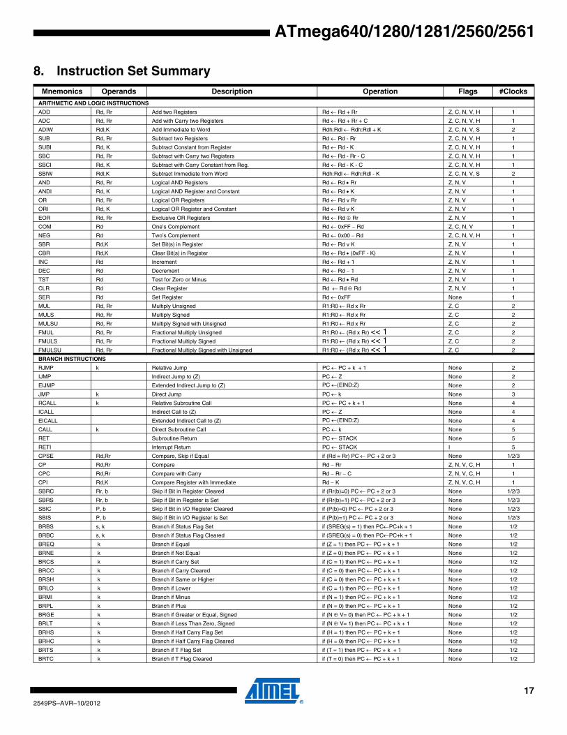
8. Instruction Set SummaryMnemonics Operands Description Operation Flags #Clocks
ARITHMETIC AND LOGIC INSTRUCTIONS
ADD Rd, Rr Add two Registers Rd ← Rd + Rr Z, C, N, V, H 1
ADC Rd, Rr Add with Carry two Registers Rd ← Rd + Rr + C Z, C, N, V, H 1
ADIW Rdl,K Add Immediate to Word Rdh:Rdl ← Rdh:Rdl + K Z, C, N, V, S 2
SUB Rd, Rr Subtract two Registers Rd ← Rd - Rr Z, C, N, V, H 1
SUBI Rd, K Subtract Constant from Register Rd ← Rd - K Z, C, N, V, H 1
SBC Rd, Rr Subtract with Carry two Registers Rd ← Rd - Rr - C Z, C, N, V, H 1
SBCI Rd, K Subtract with Carry Constant from Reg. Rd ← Rd - K - C Z, C, N, V, H 1
SBIW Rdl,K Subtract Immediate from Word Rdh:Rdl ← Rdh:Rdl - K Z, C, N, V, S 2
AND Rd, Rr Logical AND Registers Rd ← Rd • Rr Z, N, V 1
ANDI Rd, K Logical AND Register and Constant Rd ← Rd • K Z, N, V 1
OR Rd, Rr Logical OR Registers Rd ← Rd v Rr Z, N, V 1
ORI Rd, K Logical OR Register and Constant Rd ← Rd v K Z, N, V 1
EOR Rd, Rr Exclusive OR Registers Rd ← Rd ⊕ Rr Z, N, V 1
COM Rd One’s Complement Rd ← 0xFF − Rd Z, C, N, V 1
NEG Rd Two’s Complement Rd ← 0x00 − Rd Z, C, N, V, H 1
SBR Rd,K Set Bit(s) in Register Rd ← Rd v K Z, N, V 1
CBR Rd,K Clear Bit(s) in Register Rd ← Rd • (0xFF - K) Z, N, V 1
INC Rd Increment Rd ← Rd + 1 Z, N, V 1
DEC Rd Decrement Rd ← Rd − 1 Z, N, V 1
TST Rd Test for Zero or Minus Rd ← Rd • Rd Z, N, V 1
CLR Rd Clear Register Rd ← Rd ⊕ Rd Z, N, V 1
SER Rd Set Register Rd ← 0xFF None 1
MUL Rd, Rr Multiply Unsigned R1:R0 ← Rd x Rr Z, C 2
MULS Rd, Rr Multiply Signed R1:R0 ← Rd x Rr Z, C 2
MULSU Rd, Rr Multiply Signed with Unsigned R1:R0 ← Rd x Rr Z, C 2
FMUL Rd, Rr Fractional Multiply Unsigned R1:R0 ← (Rd x Rr) << 1 Z, C 2
FMULS Rd, Rr Fractional Multiply Signed R1:R0 ← (Rd x Rr) << 1 Z, C 2
FMULSU Rd, Rr Fractional Multiply Signed with Unsigned R1:R0 ← (Rd x Rr) << 1 Z, C 2
BRANCH INSTRUCTIONS
RJMP k Relative Jump PC ← PC + k + 1 None 2
IJMP Indirect Jump to (Z) PC ← Z None 2
EIJMP Extended Indirect Jump to (Z) PC ←(EIND:Z) None 2
JMP k Direct Jump PC ← k None 3
RCALL k Relative Subroutine Call PC ← PC + k + 1 None 4
ICALL Indirect Call to (Z) PC ← Z None 4
EICALL Extended Indirect Call to (Z) PC ←(EIND:Z) None 4
CALL k Direct Subroutine Call PC ← k None 5
RET Subroutine Return PC ← STACK None 5
RETI Interrupt Return PC ← STACK I 5
CPSE Rd,Rr Compare, Skip if Equal if (Rd = Rr) PC ← PC + 2 or 3 None 1/2/3
CP Rd,Rr Compare Rd − Rr Z, N, V, C, H 1
CPC Rd,Rr Compare with Carry Rd − Rr − C Z, N, V, C, H 1
CPI Rd,K Compare Register with Immediate Rd − K Z, N, V, C, H 1
SBRC Rr, b Skip if Bit in Register Cleared if (Rr(b)=0) PC ← PC + 2 or 3 None 1/2/3
SBRS Rr, b Skip if Bit in Register is Set if (Rr(b)=1) PC ← PC + 2 or 3 None 1/2/3
SBIC P, b Skip if Bit in I/O Register Cleared if (P(b)=0) PC ← PC + 2 or 3 None 1/2/3
SBIS P, b Skip if Bit in I/O Register is Set if (P(b)=1) PC ← PC + 2 or 3 None 1/2/3
BRBS s, k Branch if Status Flag Set if (SREG(s) = 1) then PC←PC+k + 1 None 1/2
BRBC s, k Branch if Status Flag Cleared if (SREG(s) = 0) then PC←PC+k + 1 None 1/2
BREQ k Branch if Equal if (Z = 1) then PC ← PC + k + 1 None 1/2
BRNE k Branch if Not Equal if (Z = 0) then PC ← PC + k + 1 None 1/2
BRCS k Branch if Carry Set if (C = 1) then PC ← PC + k + 1 None 1/2
BRCC k Branch if Carry Cleared if (C = 0) then PC ← PC + k + 1 None 1/2
BRSH k Branch if Same or Higher if (C = 0) then PC ← PC + k + 1 None 1/2
BRLO k Branch if Lower if (C = 1) then PC ← PC + k + 1 None 1/2
BRMI k Branch if Minus if (N = 1) then PC ← PC + k + 1 None 1/2
BRPL k Branch if Plus if (N = 0) then PC ← PC + k + 1 None 1/2
BRGE k Branch if Greater or Equal, Signed if (N ⊕ V= 0) then PC ← PC + k + 1 None 1/2
BRLT k Branch if Less Than Zero, Signed if (N ⊕ V= 1) then PC ← PC + k + 1 None 1/2
BRHS k Branch if Half Carry Flag Set if (H = 1) then PC ← PC + k + 1 None 1/2
BRHC k Branch if Half Carry Flag Cleared if (H = 0) then PC ← PC + k + 1 None 1/2
BRTS k Branch if T Flag Set if (T = 1) then PC ← PC + k + 1 None 1/2
BRTC k Branch if T Flag Cleared if (T = 0) then PC ← PC + k + 1 None 1/2
172549PS–AVR–10/2012
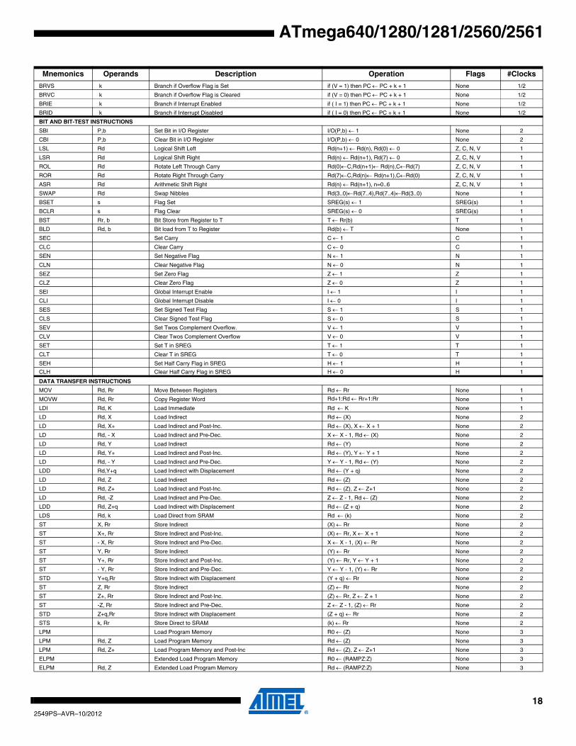
ATmega640/1280/1281/2560/2561
BRVS k Branch if Overflow Flag is Set if (V = 1) then PC ← PC + k + 1 None 1/2
BRVC k Branch if Overflow Flag is Cleared if (V = 0) then PC ← PC + k + 1 None 1/2
BRIE k Branch if Interrupt Enabled if ( I = 1) then PC ← PC + k + 1 None 1/2
BRID k Branch if Interrupt Disabled if ( I = 0) then PC ← PC + k + 1 None 1/2
BIT AND BIT-TEST INSTRUCTIONS
SBI P,b Set Bit in I/O Register I/O(P,b) ← 1 None 2
CBI P,b Clear Bit in I/O Register I/O(P,b) ← 0 None 2
LSL Rd Logical Shift Left Rd(n+1) ← Rd(n), Rd(0) ← 0 Z, C, N, V 1
LSR Rd Logical Shift Right Rd(n) ← Rd(n+1), Rd(7) ← 0 Z, C, N, V 1
ROL Rd Rotate Left Through Carry Rd(0)←C,Rd(n+1)← Rd(n),C←Rd(7) Z, C, N, V 1
ROR Rd Rotate Right Through Carry Rd(7)←C,Rd(n)← Rd(n+1),C←Rd(0) Z, C, N, V 1
ASR Rd Arithmetic Shift Right Rd(n) ← Rd(n+1), n=0..6 Z, C, N, V 1
SWAP Rd Swap Nibbles Rd(3..0)←Rd(7..4),Rd(7..4)←Rd(3..0) None 1
BSET s Flag Set SREG(s) ← 1 SREG(s) 1
BCLR s Flag Clear SREG(s) ← 0 SREG(s) 1
BST Rr, b Bit Store from Register to T T ← Rr(b) T 1
BLD Rd, b Bit load from T to Register Rd(b) ← T None 1
SEC Set Carry C ← 1 C 1
CLC Clear Carry C ← 0 C 1
SEN Set Negative Flag N ← 1 N 1
CLN Clear Negative Flag N ← 0 N 1
SEZ Set Zero Flag Z ← 1 Z 1
CLZ Clear Zero Flag Z ← 0 Z 1
SEI Global Interrupt Enable I ← 1 I 1
CLI Global Interrupt Disable I ← 0 I 1
SES Set Signed Test Flag S ← 1 S 1
CLS Clear Signed Test Flag S ← 0 S 1
SEV Set Twos Complement Overflow. V ← 1 V 1
CLV Clear Twos Complement Overflow V ← 0 V 1
SET Set T in SREG T ← 1 T 1
CLT Clear T in SREG T ← 0 T 1
SEH Set Half Carry Flag in SREG H ← 1 H 1
CLH Clear Half Carry Flag in SREG H ← 0 H 1
DATA TRANSFER INSTRUCTIONS
MOV Rd, Rr Move Between Registers Rd ← Rr None 1
MOVW Rd, Rr Copy Register Word Rd+1:Rd ← Rr+1:Rr None 1
LDI Rd, K Load Immediate Rd ← K None 1
LD Rd, X Load Indirect Rd ← (X) None 2
LD Rd, X+ Load Indirect and Post-Inc. Rd ← (X), X ← X + 1 None 2
LD Rd, - X Load Indirect and Pre-Dec. X ← X - 1, Rd ← (X) None 2
LD Rd, Y Load Indirect Rd ← (Y) None 2
LD Rd, Y+ Load Indirect and Post-Inc. Rd ← (Y), Y ← Y + 1 None 2
LD Rd, - Y Load Indirect and Pre-Dec. Y ← Y - 1, Rd ← (Y) None 2
LDD Rd,Y+q Load Indirect with Displacement Rd ← (Y + q) None 2
LD Rd, Z Load Indirect Rd ← (Z) None 2
LD Rd, Z+ Load Indirect and Post-Inc. Rd ← (Z), Z ← Z+1 None 2
LD Rd, -Z Load Indirect and Pre-Dec. Z ← Z - 1, Rd ← (Z) None 2
LDD Rd, Z+q Load Indirect with Displacement Rd ← (Z + q) None 2
LDS Rd, k Load Direct from SRAM Rd ← (k) None 2
ST X, Rr Store Indirect (X) ← Rr None 2
ST X+, Rr Store Indirect and Post-Inc. (X) ← Rr, X ← X + 1 None 2
ST - X, Rr Store Indirect and Pre-Dec. X ← X - 1, (X) ← Rr None 2
ST Y, Rr Store Indirect (Y) ← Rr None 2
ST Y+, Rr Store Indirect and Post-Inc. (Y) ← Rr, Y ← Y + 1 None 2
ST - Y, Rr Store Indirect and Pre-Dec. Y ← Y - 1, (Y) ← Rr None 2
STD Y+q,Rr Store Indirect with Displacement (Y + q) ← Rr None 2
ST Z, Rr Store Indirect (Z) ← Rr None 2
ST Z+, Rr Store Indirect and Post-Inc. (Z) ← Rr, Z ← Z + 1 None 2
ST -Z, Rr Store Indirect and Pre-Dec. Z ← Z - 1, (Z) ← Rr None 2
STD Z+q,Rr Store Indirect with Displacement (Z + q) ← Rr None 2
STS k, Rr Store Direct to SRAM (k) ← Rr None 2
LPM Load Program Memory R0 ← (Z) None 3
LPM Rd, Z Load Program Memory Rd ← (Z) None 3
LPM Rd, Z+ Load Program Memory and Post-Inc Rd ← (Z), Z ← Z+1 None 3
ELPM Extended Load Program Memory R0 ← (RAMPZ:Z) None 3
ELPM Rd, Z Extended Load Program Memory Rd ← (RAMPZ:Z) None 3
Mnemonics Operands Description Operation Flags #Clocks
182549PS–AVR–10/2012
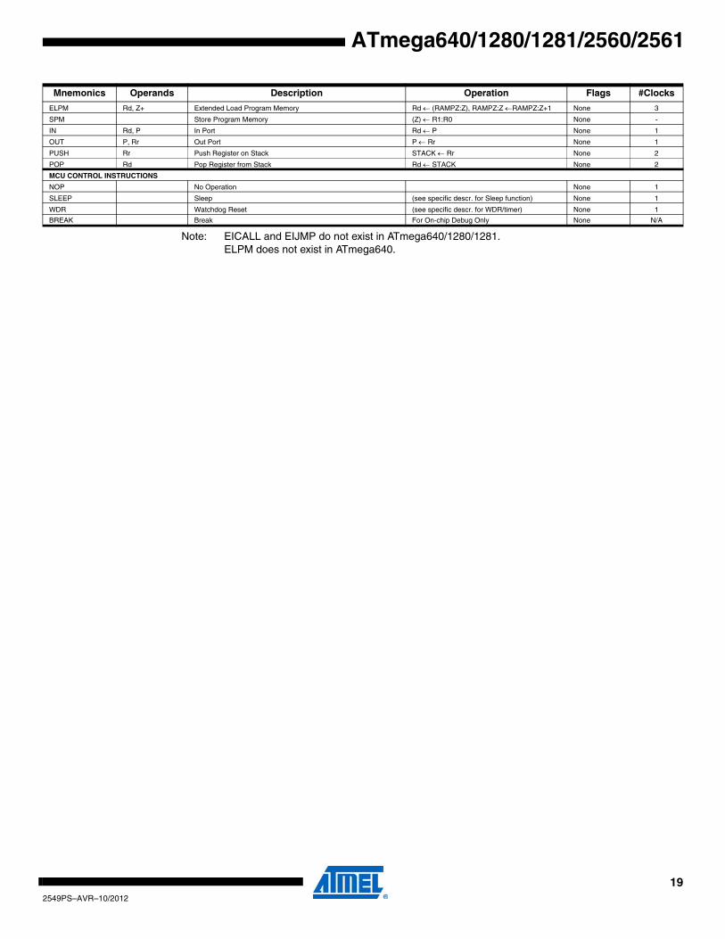
ATmega640/1280/1281/2560/2561
Note: EICALL and EIJMP do not exist in ATmega640/1280/1281.ELPM does not exist in ATmega640.
ELPM Rd, Z+ Extended Load Program Memory Rd ← (RAMPZ:Z), RAMPZ:Z ←RAMPZ:Z+1 None 3
SPM Store Program Memory (Z) ← R1:R0 None -
IN Rd, P In Port Rd ← P None 1
OUT P, Rr Out Port P ← Rr None 1
PUSH Rr Push Register on Stack STACK ← Rr None 2
POP Rd Pop Register from Stack Rd ← STACK None 2
MCU CONTROL INSTRUCTIONS
NOP No Operation None 1
SLEEP Sleep (see specific descr. for Sleep function) None 1
WDR Watchdog Reset (see specific descr. for WDR/timer) None 1
BREAK Break For On-chip Debug Only None N/A
Mnemonics Operands Description Operation Flags #Clocks
192549PS–AVR–10/2012
ATmega640/1280/1281/2560/2561
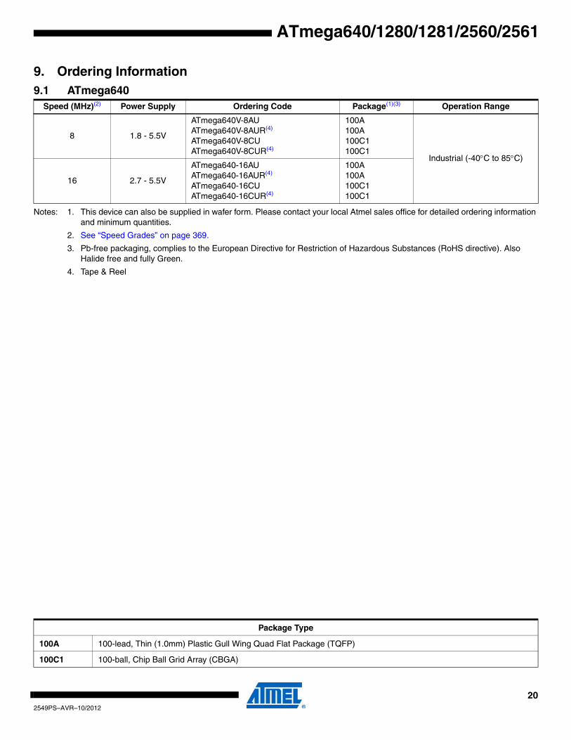
9. Ordering Information
Notes: 1. This device can also be supplied in wafer form. Please contact your local Atmel sales office for detailed ordering information and minimum quantities.
2. See “Speed Grades” on page 369.
3. Pb-free packaging, complies to the European Directive for Restriction of Hazardous Substances (RoHS directive). Also Halide free and fully Green.
4. Tape & Reel
9.1 ATmega640Speed (MHz)(2) Power Supply Ordering Code Package(1)(3) Operation Range
8 1.8 - 5.5V
ATmega640V-8AUATmega640V-8AUR(4)
ATmega640V-8CUATmega640V-8CUR(4)
100A100A100C1100C1
Industrial (-40°C to 85°C)
16 2.7 - 5.5V
ATmega640-16AUATmega640-16AUR(4)
ATmega640-16CUATmega640-16CUR(4)
100A100A100C1100C1
Package Type
100A 100-lead, Thin (1.0mm) Plastic Gull Wing Quad Flat Package (TQFP)
100C1 100-ball, Chip Ball Grid Array (CBGA)
202549PS–AVR–10/2012
ATmega640/1280/1281/2560/2561
Notes: 1. This device can also be supplied in wafer form. Please contact your local Atmel sales office for detailed ordering information and minimum quantities.
2. See “Speed Grades” on page 369.
3. Pb-free packaging, complies to the European Directive for Restriction of Hazardous Substances (RoHS directive). Also Halide free and fully Green.
4. Tape & Reel
9.2 ATmega1280Speed (MHz)(2) Power Supply Ordering Code Package(1)(3) Operation Range
8 1.8V - 5.5V
ATmega1280V-8AUATmega1280V-8AUR(4)
ATmega1280V-8CUATmega1280V-8CUR(4)
100A100A100C1100C1
Industrial (-40°C to 85°C)
16 2.7V - 5.5V
ATmega1280-16AUATmega1280-16AUR(4)
ATmega1280-16CUATmega1280-16CUR(4)
100A100A100C1100C1
Package Type
100A 100-lead, Thin (1.0mm) Plastic Gull Wing Quad Flat Package (TQFP)
100C1 100-ball, Chip Ball Grid Array (CBGA)
212549PS–AVR–10/2012
ATmega640/1280/1281/2560/2561
Notes: 1. This device can also be supplied in wafer form. Please contact your local Atmel sales office for detailed ordering information and minimum quantities.
2. See “Speed Grades” on page 369.
3. Pb-free packaging, complies to the European Directive for Restriction of Hazardous Substances (RoHS directive). Also Halide free and fully Green.
4. Tape & Reel
9.3 ATmega1281Speed (MHz)(2) Power Supply Ordering Code Package(1)(3) Operation Range
8 1.8 - 5.5V
ATmega1281V-8AUATmega1281V-8AUR(4)
ATmega1281V-8MUATmega1281V-8MUR(4)
64A64A64M264M2 Industrial
(-40°C to 85°C)
16 2.7 - 5.5V
ATmega1281-16AUATmega1281-16AUR(4)
ATmega1281-16MUATmega1281-16MUR(4)
64A64A64M264M2
Package Type
64A 64-lead, Thin (1.0mm) Plastic Gull Wing Quad Flat Package (TQFP)
64M2 64-pad, 9mm × 9mm × 1.0mm Body, Quad Flat No-lead/Micro Lead Frame Package (QFN/MLF)
222549PS–AVR–10/2012

ATmega640/1280/1281/2560/2561
Notes: 1. This device can also be supplied in wafer form. Please contact your local Atmel sales office for detailed ordering information and minimum quantities.
2. See “Speed Grades” on page 369.
3. Pb-free packaging, complies to the European Directive for Restriction of Hazardous Substances (RoHS directive). Also Halide free and fully Green.
4. Tape & Reel
9.4 ATmega2560Speed (MHz)(2) Power Supply Ordering Code Package(1)(3) Operation Range
8 1.8V - 5.5V
ATmega2560V-8AUATmega2560V-8AUR(4)
ATmega2560V-8CUATmega2560V-8CUR(4)
100A100A100C1100C1
Industrial (-40°C to 85°C)
16 4.5V - 5.5V
ATmega2560-16AUATmega2560-16AUR(4)
ATmega2560-16CUATmega2560-16CUR(4)
100A100A100C1100C1
Package Type
100A 100-lead, Thin (1.0mm) Plastic Gull Wing Quad Flat Package (TQFP)
100C1 100-ball, Chip Ball Grid Array (CBGA)
232549PS–AVR–10/2012
ATmega640/1280/1281/2560/2561
Notes: 1. This device can also be supplied in wafer form. Please contact your local Atmel sales office for detailed ordering information and minimum quantities.
2. See “Speed Grades” on page 369.
3. Pb-free packaging, complies to the European Directive for Restriction of Hazardous Substances (RoHS directive). Also Halide free and fully Green.
4. Tape & Reel
9.5 ATmega2561Speed (MHz)(2) Power Supply Ordering Code Package(1)(3) Operation Range
8 1.8V - 5.5V
ATmega1281V-8AUATmega1281V-8AUR(4)
ATmega1281V-8MUATmega1281V-8MUR(4)
64A64A64M264M2 Industrial
(-40°C to 85°C)
16 4.5V - 5.5V
ATmega1281-16AUATmega1281-16AUR(4)
ATmega1281-16MUATmega1281-16MUR(4)
64A64A64M264M2
Package Type
64A 64-lead, Thin (1.0mm) Plastic Gull Wing Quad Flat Package (TQFP)
64M2 64-pad, 9mm × 9mm × 1.0mm Body, Quad Flat No-lead/Micro Lead Frame Package (QFN/MLF)
242549PS–AVR–10/2012
ATmega640/1280/1281/2560/2561
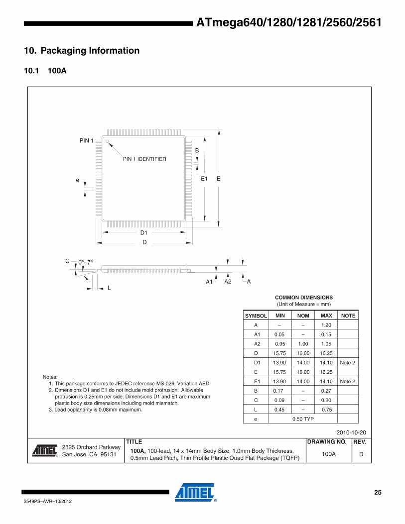
10. Packaging Information
10.1 100A
2325 Orchard Parkway San Jose, CA 95131
TITLE DRAWING NO.
R
REV.
100A, 100-lead, 14 x 14mm Body Size, 1.0mm Body Thickness,0.5mm Lead Pitch, Thin Profile Plastic Quad Flat Package (TQFP)
D100A
2010-10-20
PIN 1 IDENTIFIER
0°~7°
PIN 1
L
C
A1 A2 A
D1
D
e E1 E
B
A – – 1.20
A1 0.05 – 0.15
A2 0.95 1.00 1.05
D 15.75 16.00 16.25
D1 13.90 14.00 14.10 Note 2
E 15.75 16.00 16.25
E1 13.90 14.00 14.10 Note 2
B 0.17 – 0.27
C 0.09 – 0.20
L 0.45 – 0.75
e 0.50 TYP
Notes: 1. This package conforms to JEDEC reference MS-026, Variation AED. 2. Dimensions D1 and E1 do not include mold protrusion. Allowable protrusion is 0.25mm per side. Dimensions D1 and E1 are maximum plastic body size dimensions including mold mismatch. 3. Lead coplanarity is 0.08mm maximum.
COMMON DIMENSIONS(Unit of Measure = mm)
SYMBOL MIN NOM MAX NOTE
252549PS–AVR–10/2012
ATmega640/1280/1281/2560/2561
10.2 100C1
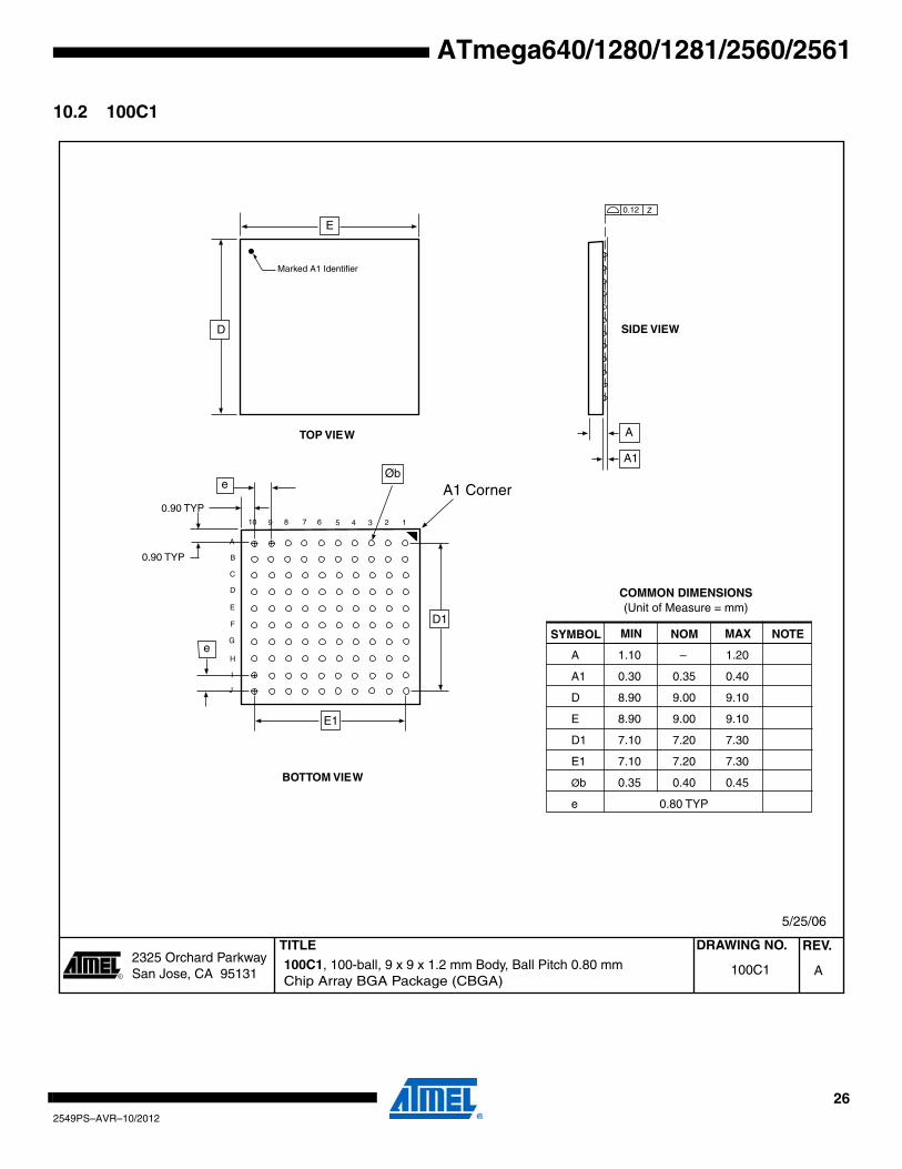
2325 Orchard Parkway San Jose, CA 95131
TITLE DRAWING NO.
R
REV. 100C1, 100-ball, 9 x 9 x 1.2 mm Body, Ball Pitch 0.80 mm Chip Array BGA Package (CBGA)
A100C1
5/25/06
TOP VIEW
SIDE VIEW
BOTTOM VIEW
COMMON DIMENSIONS(Unit of Measure = mm)
SYMBOL MIN NOM MAX NOTE
A 1.10 – 1.20
A1 0.30 0.35 0.40
D 8.90 9.00 9.10
E 8.90 9.00 9.10
D1 7.10 7.20 7.30
E1 7.10 7.20 7.30
Øb 0.35 0.40 0.45
e 0.80 TYP
Marked A1 Identifier
12345678
A
B
C
D
E
9
F
G
H
I
J
10
0.90 TYP
0.90 TYP
A1 Corner
0.12 Z
E
D
e
e
Øb
A
A1
E1
D1
262549PS–AVR–10/2012
ATmega640/1280/1281/2560/2561
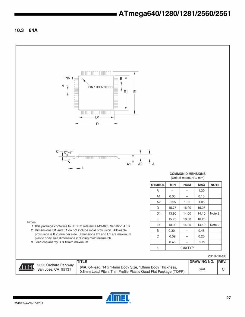
10.3 64A
2325 Orchard Parkway San Jose, CA 95131
TITLE DRAWING NO.
R
REV.
64A, 64-lead, 14 x 14mm Body Size, 1.0mm Body Thickness,0.8mm Lead Pitch, Thin Profile Plastic Quad Flat Package (TQFP)
C64A
2010-10-20
PIN 1 IDENTIFIER
0°~7°
PIN 1
L
C
A1 A2 A
D1
D
e
E1 E
B
COMMON DIMENSIONS(Unit of measure = mm)
SYMBOL MIN NOM MAX NOTE
Notes: 1.This package conforms to JEDEC reference MS-026, Variation AEB. 2. Dimensions D1 and E1 do not include mold protrusion. Allowable protrusion is 0.25mm per side. Dimensions D1 and E1 are maximum plastic body size dimensions including mold mismatch. 3. Lead coplanarity is 0.10mm maximum.
A – – 1.20
A1 0.05 – 0.15
A2 0.95 1.00 1.05
D 15.75 16.00 16.25
D1 13.90 14.00 14.10 Note 2
E 15.75 16.00 16.25
E1 13.90 14.00 14.10 Note 2
B 0.30 – 0.45
C 0.09 – 0.20
L 0.45 – 0.75
e 0.80 TYP
272549PS–AVR–10/2012
ATmega640/1280/1281/2560/2561
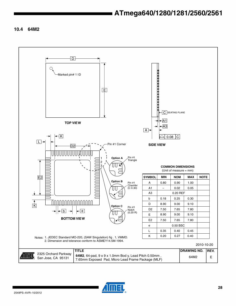
10.4 64M2
2325 Orchard Parkway San Jose, CA 95131
TITLE DRAWING NO.
R
REV. 64M2, 64-pad, 9 x 9 x 1.0mm Bod y, Lead Pitch 0.50mm , E64M2
2010-10-20
COMMON DIMENSIONS(Unit of measure = mm)
SYMBOL MIN NOM MAX NOTE
A 0.80 0.90 1.00
A1 – 0.02 0.05
b
0.18 0.25 0.30
D
D2
7.50 7.65 7.80
8.90 9.00 9.10
8.90 9.00 9.10
E
E2
7.50 7.65 7.80
e
0.50 BSC
L 0.35 0.40
0.45
TOP VIEW
SIDE VIEW
BOTTOM VIEW
D
E
Marked pin# 1 ID
SEATING PLANE
A1
C
A
C0.08
123
K 0.20 0.27 0.40
2. Dimension and tolerance conform to ASMEY14.5M-1994.
0.20 REFA3
A3
E2
D2
b e
Pin #1 CornerL
Pin #1 Triangle
Pin #1 Chamfer(C 0.30)
Option A
Option B
Pin #1 Notch(0.20 R)
Option C
K
K
Notes: 1. JEDEC Standard MO-220, (SAW Singulation) fig . 1, VMMD.
7.65mm Exposed Pad, Micro Lead Frame Package (MLF)
282549PS–AVR–10/2012
ATmega640/1280/1281/2560/2561
11. Errata
11.1 ATmega640 rev. B• Inaccurate ADC conversion in differential mode with 200× gain• High current consumption in sleep mode
1. Inaccurate ADC conversion in differential mode with 200× gainWith AVCC <3.6V, random conversions will be inaccurate. Typical absolute accuracy mayreach 64 LSB.
Problem Fix/WorkaroundNone.
2. High current consumption in sleep modeIf a pending interrupt cannot wake the part up from the selected sleep mode, the currentconsumption will increase during sleep when executing the SLEEP instruction directly aftera SEI instruction.
Problem Fix/WorkaroundBefore entering sleep, interrupts not used to wake the part from the sleep mode should bedisabled.
11.2 ATmega640 rev. A• Inaccurate ADC conversion in differential mode with 200× gain• High current consumption in sleep mode
1. Inaccurate ADC conversion in differential mode with 200× gainWith AVCC <3.6V, random conversions will be inaccurate. Typical absolute accuracy mayreach 64 LSB.
Problem Fix/WorkaroundNone.
2. High current consumption in sleep modeIf a pending interrupt cannot wake the part up from the selected sleep mode, the currentconsumption will increase during sleep when executing the SLEEP instruction directly aftera SEI instruction.
Problem Fix/WorkaroundBefore entering sleep, interrupts not used to wake the part from the sleep mode should bedisabled.
11.3 ATmega1280 rev. B• Inaccurate ADC conversion in differential mode with 200× gain• High current consumption in sleep mode
1. Inaccurate ADC conversion in differential mode with 200× gainWith AVCC <3.6V, random conversions will be inaccurate. Typical absolute accuracy mayreach 64 LSB.
292549PS–AVR–10/2012
ATmega640/1280/1281/2560/2561
Problem Fix/WorkaroundNone.
2. High current consumption in sleep modeIf a pending interrupt cannot wake the part up from the selected sleep mode, the currentconsumption will increase during sleep when executing the SLEEP instruction directly aftera SEI instruction.
Problem Fix/WorkaroundBefore entering sleep, interrupts not used to wake the part from the sleep mode should bedisabled.
11.4 ATmega1280 rev. A• Inaccurate ADC conversion in differential mode with 200× gain• High current consumption in sleep mode
1. Inaccurate ADC conversion in differential mode with 200× gainWith AVCC <3.6V, random conversions will be inaccurate. Typical absolute accuracy mayreach 64 LSB.
Problem Fix/WorkaroundNone.
2. High current consumption in sleep modeIf a pending interrupt cannot wake the part up from the selected sleep mode, the currentconsumption will increase during sleep when executing the SLEEP instruction directly aftera SEI instruction.
Problem Fix/WorkaroundBefore entering sleep, interrupts not used to wake the part from the sleep mode should bedisabled.
11.5 ATmega1281 rev. B• Inaccurate ADC conversion in differential mode with 200× gain• High current consumption in sleep mode
1. Inaccurate ADC conversion in differential mode with 200× gainWith AVCC <3.6V, random conversions will be inaccurate. Typical absolute accuracy mayreach 64 LSB.
Problem Fix/WorkaroundNone.
2. High current consumption in sleep modeIf a pending interrupt cannot wake the part up from the selected sleep mode, the currentconsumption will increase during sleep when executing the SLEEP instruction directly aftera SEI instruction.
Problem Fix/WorkaroundBefore entering sleep, interrupts not used to wake the part from the sleep mode should bedisabled.
302549PS–AVR–10/2012
ATmega640/1280/1281/2560/2561
11.6 ATmega1281 rev. A• Inaccurate ADC conversion in differential mode with 200× gain• High current consumption in sleep mode
1. Inaccurate ADC conversion in differential mode with 200× gainWith AVCC <3.6V, random conversions will be inaccurate. Typical absolute accuracy mayreach 64 LSB.
Problem Fix/WorkaroundNone.
2. High current consumption in sleep modeIf a pending interrupt cannot wake the part up from the selected sleep mode, the currentconsumption will increase during sleep when executing the SLEEP instruction directly aftera SEI instruction.
Problem Fix/WorkaroundBefore entering sleep, interrupts not used to wake the part from the sleep mode should bedisabled.
11.7 ATmega2560 rev. FNot sampled.
11.8 ATmega2560 rev. ENo known errata.
11.9 ATmega2560 rev. DNot sampled.
11.10 ATmega2560 rev. C• High current consumption in sleep mode
1. High current consumption in sleep modeIf a pending interrupt cannot wake the part up from the selected sleep mode, the currentconsumption will increase during sleep when executing the SLEEP instruction directly aftera SEI instruction.
Problem Fix/WorkaroundBefore entering sleep, interrupts not used to wake the part from the sleep mode should bedisabled.
11.11 ATmega2560 rev. BNot sampled.
312549PS–AVR–10/2012
ATmega640/1280/1281/2560/2561
11.12 ATmega2560 rev. A• Non-Read-While-Write area of flash not functional• Part does not work under 2.4 volts• Incorrect ADC reading in differential mode• Internal ADC reference has too low value• IN/OUT instructions may be executed twice when Stack is in external RAM• EEPROM read from application code does not work in Lock Bit Mode 3
1. Non-Read-While-Write area of flash not functionalThe Non-Read-While-Write area of the flash is not working as expected. The problem isrelated to the speed of the part when reading the flash of this area.
Problem Fix/Workaround- Only use the first 248K of the flash.
- If boot functionality is needed, run the code in the Non-Read-While-Write area at maximum1/4th of the maximum frequency of the device at any given voltage. This is done by writingthe CLKPR register before entering the boot section of the code.
2. Part does not work under 2.4 voltsThe part does not execute code correctly below 2.4 volts.
Problem Fix/WorkaroundDo not use the part at voltages below 2.4 volts.
3. Incorrect ADC reading in differential modeThe ADC has high noise in differential mode. It can give up to 7 LSB error.
Problem Fix/WorkaroundUse only the 7 MSB of the result when using the ADC in differential mode.
4. Internal ADC reference has too low valueThe internal ADC reference has a value lower than specified.
Problem Fix/Workaround- Use AVCC or external reference.
- The actual value of the reference can be measured by applying a known voltage to theADC when using the internal reference. The result when doing later conversions can then becalibrated.
5. IN/OUT instructions may be executed twice when Stack is in external RAMIf either an IN or an OUT instruction is executed directly before an interrupt occurs and thestack pointer is located in external ram, the instruction will be executed twice. In some casesthis will cause a problem, for example:
- If reading SREG it will appear that the I-flag is cleared.
- If writing to the PIN registers, the port will toggle twice.
- If reading registers with interrupt flags, the flags will appear to be cleared.
322549PS–AVR–10/2012
ATmega640/1280/1281/2560/2561
Problem Fix/WorkaroundThere are two application work-arounds, where selecting one of them, will be omitting theissue:
- Replace IN and OUT with LD/LDS/LDD and ST/STS/STD instructions.
- Use internal RAM for stack pointer.
6. EEPROM read from application code does not work in Lock Bit Mode 3When the Memory Lock Bits LB2 and LB1 are programmed to mode 3, EEPROM read doesnot work from the application code.
Problem Fix/WorkaroundDo not set Lock Bit Protection Mode 3 when the application code needs to read fromEEPROM.
11.13 ATmega2561 rev. FNot sampled.
11.14 ATmega2561 rev. ENo known errata.
11.15 ATmega2561 rev. DNot sampled.
11.16 ATmega2561 rev. C• High current consumption in sleep mode.
1. High current consumption in sleep modeIf a pending interrupt cannot wake the part up from the selected sleep mode, the currentconsumption will increase during sleep when executing the SLEEP instruction directly aftera SEI instruction.
Problem Fix/WorkaroundBefore entering sleep, interrupts not used to wake the part from the sleep mode should bedisabled.
11.17 ATmega2561 rev. B
Not sampled.
11.18 ATmega2561 rev. A• Non-Read-While-Write area of flash not functional• Part does not work under 2.4 Volts• Incorrect ADC reading in differential mode• Internal ADC reference has too low value• IN/OUT instructions may be executed twice when Stack is in external RAM• EEPROM read from application code does not work in Lock Bit Mode 3
332549PS–AVR–10/2012
ATmega640/1280/1281/2560/2561
1. Non-Read-While-Write area of flash not functionalThe Non-Read-While-Write area of the flash is not working as expected. The problem isrelated to the speed of the part when reading the flash of this area.
Problem Fix/Workaround- Only use the first 248K of the flash.
- If boot functionality is needed, run the code in the Non-Read-While-Write area at maximum1/4th of the maximum frequency of the device at any given voltage. This is done by writingthe CLKPR register before entering the boot section of the code.
2. Part does not work under 2.4 voltsThe part does not execute code correctly below 2.4 volts.
Problem Fix/WorkaroundDo not use the part at voltages below 2.4 volts.
3. Incorrect ADC reading in differential modeThe ADC has high noise in differential mode. It can give up to 7 LSB error.
Problem Fix/WorkaroundUse only the 7 MSB of the result when using the ADC in differential mode.
4. Internal ADC reference has too low valueThe internal ADC reference has a value lower than specified.
Problem Fix/Workaround- Use AVCC or external reference.
- The actual value of the reference can be measured by applying a known voltage to theADC when using the internal reference. The result when doing later conversions can then becalibrated.
5. IN/OUT instructions may be executed twice when Stack is in external RAMIf either an IN or an OUT instruction is executed directly before an interrupt occurs and thestack pointer is located in external ram, the instruction will be executed twice. In some casesthis will cause a problem, for example:
- If reading SREG it will appear that the I-flag is cleared.
- If writing to the PIN registers, the port will toggle twice.
- If reading registers with interrupt flags, the flags will appear to be cleared.
Problem Fix/WorkaroundThere are two application workarounds, where selecting one of them, will be omitting theissue:
- Replace IN and OUT with LD/LDS/LDD and ST/STS/STD instructions.
- Use internal RAM for stack pointer.
6. EEPROM read from application code does not work in Lock Bit Mode 3When the Memory Lock Bits LB2 and LB1 are programmed to mode 3, EEPROM read doesnot work from the application code.
342549PS–AVR–10/2012

ATmega640/1280/1281/2560/2561
Problem Fix/WorkaroundDo not set Lock Bit Protection Mode 3 when the application code needs to read fromEEPROM.
352549PS–AVR–10/2012
ATmega640/1280/1281/2560/2561
12. Datasheet Revision HistoryPlease note that the referring page numbers in this section are referring to this document.Thereferring revision in this section are referring to the document revision.
12.1 Rev. 2549P-10/2012
12.2 Rev. 2549O-05/12
12.3 Rev. 2549N-05/11
12.4 Rev. 2549M-09/10
1. Replaced drawing in 10.4 “64M2” on page 28.
2. Former page 439 has been deleted as the content of this page did not belong there (same pageas the last page).
3. Some small correction made in the setup.
1. The datasheet changed status from Preliminary to Complete. Removed “Preliminary” from thefront page.
2. Replaced Figure 10-3 on page 46 by a new one.
3. Updated the last page to include the new address for Atmel Japan site.
1. Added Atmel QTouch Library Support and QTouch Sensing Capablity Features
2. Updated Cross-reference in “Bit 5, 2:0 - WDP3:0: Watchdog Timer Prescaler 3, 2, 1 and 0” onpage 68
3. Updated Assembly codes in section “USART Initialization” on page 210
4. Added “Standard Power-On Reset” on page 372.5. Added “Enhanced Power-On Reset” on page 373.
6. Updated Figure 32-13 on page 393
7. Updated “Ordering Information” on page 20 to include Tape & Reel devices.
1. Updated typos in Figure 26-9 on page 285 and in Figure 26-10 on page 285.
2. Note is added below Table 1-1 on page 3.
3. The values for “typical characteristics” in Table 31-9 on page 377 and Table 31-10 on page 378,has been rounded.
4. Units for tRST and tBOD in Table 31-3 on page 372 have been changed from “ns” to “µs”.5. The figure text for Table 31-2 on page 371 has been changed.
6. Text in first column in Table 30-3 on page 336 has been changed from “Fuse Low Byte” to“Extended Fuse Byte”.
7. The text in “Power Reduction Register” on page 54 has been changed.
8. The value of the inductor in Figure 26-9 on page 285 and Figure 26-10 on page 285 has beenchanged to 10 µH.
9. “Port A” has been changed into “Port K” in the first paragraph of “Features” on page 275.
10. Minimum wait delay for tWD_EEPROM in Table 30-16 on page 351 has been changed from9.0ms to 3.6ms
11. Dimension A3 is added in “64M2” on page 28.12. Several cross-references are corrected.
362549PS–AVR–10/2012
ATmega640/1280/1281/2560/2561
12.5 Rev. 2549L-08/07
12.6 Rev. 2549K-01/07
12.7 Rev. 2549J-09/06
13. “COM0A1:0” on page 130 is corrected to “COM0B1:0”.
14. Corrected some Figure and Table numbering.
15. Updated Section 10.6 “Low Frequency Crystal Oscillator” on page 45.
1. Updated note in Table 10-11 on page 47.
2. Updated Table 10-3 on page 43, Table 10-5 on page 44, Table 10-9 on page 47.
3. Updated typos in “DC Characteristics” on page 3674. Updated “Clock Characteristics” on page 371
5. Updated “External Clock Drive” on page 371.
6. Added “System and Reset Characteristics” on page 372.7. Updated “SPI Timing Characteristics” on page 375.
8. Updated “ADC Characteristics – Preliminary Data” on page 377.
9. Updated ordering code in “ATmega640” on page 20.
1. Updated Table 1-1 on page 3.
2. Updated “Pin Descriptions” on page 7.3. Updated “Stack Pointer” on page 16.
4. Updated “Bit 1 – EEPE: EEPROM Programming Enable” on page 36.
5. Updated Assembly code example in “Thus, when the BOD is not enabled, after setting the ACBGbit or enabling the ADC, the user must always allow the reference to start up before the outputfrom the Analog Comparator or ADC is used. To reduce power consumption in Power-downmode, the user can avoid the three conditions above to ensure that the reference is turned offbefore entering Power-down mode.” on page 63.
6: Updated “EIMSK – External Interrupt Mask Register” on page 115.7. Updated Bit description in “PCIFR – Pin Change Interrupt Flag Register” on page 116.
8. Updated code example in “USART Initialization” on page 210.
9. Updated Figure 26-8 on page 284.10. Updated “DC Characteristics” on page 367.
1. Updated “” on page 46.2. Updated code example in “Moving Interrupts Between Application and Boot Section” on page
109.3. Updated “Timer/Counter Prescaler” on page 186.
4. Updated “Device Identification Register” on page 303.
5. Updated “Signature Bytes” on page 338.6. Updated “Instruction Set Summary” on page 17.
372549PS–AVR–10/2012
ATmega640/1280/1281/2560/2561
12.8 Rev. 2549I-07/06
12.9 Rev. 2549H-06/06
12.10 Rev. 2549G-06/06
12.11 Rev. 2549F-04/06
12.12 Rev. 2549E-04/06
1. Added “Data Retention” on page 11.
2. Updated Table 16-3 on page 129, Table 16-6 on page 130, Table 16-8 on page 131, Table 17-2on page 148, Table 17-4 on page 159, Table 17-5 on page 160, Table 20-3 on page 187, Table20-6 on page 188 and Table 20-8 on page 189.
3. Updated “Fast PWM Mode” on page 150.
1. Updated “” on page 46.
2. Updated “OSCCAL – Oscillator Calibration Register” on page 50.3. Added Table 31-1 on page 371.
1. Updated “Features” on page 1.2. Added Figure 1-2 on page 3, Table 1-1 on page 3.
3. Updated “” on page 46.
4. Updated “Power Management and Sleep Modes” on page 52.5. Updated note for Table 12-1 on page 68.
6. Updated Figure 26-9 on page 285 and Figure 26-10 on page 285.
7. Updated “Setting the Boot Loader Lock Bits by SPM” on page 324.8. Updated “Ordering Information” on page 20.
9. Added Package information “100C1” on page 26.
10. Updated “Errata” on page 29.
1. Updated Figure 9-3 on page 31, Figure 9-4 on page 31 and Figure 9-5 on page 32.
2. Updated Table 20-2 on page 187 and Table 20-3 on page 187.3. Updated Features in “ADC – Analog to Digital Converter” on page 275.
4. Updated “Fuse Bits” on page 336.
1. Updated “Features” on page 1.
2. Updated Table 12-1 on page 62.
3. Updated note for Table 12-1 on page 62.4. Updated “Bit 6 – ACBG: Analog Comparator Bandgap Select” on page 273.
5. Updated “Prescaling and Conversion Timing” on page 278.
5. Updated “Maximum speed vs. VCC” on page 373.
6. Updated “Ordering Information” on page 20.
382549PS–AVR–10/2012
ATmega640/1280/1281/2560/2561
12.13 Rev. 2549D-12/05
12.14 Rev. 2549C-09/05
12.15 Rev. 2549B-05/05
12.16 Rev. 2549A-03/05
1. Advanced Information Status changed to Preliminary.
2. Changed number of I/O Ports from 51 to 54.
3. Updatet typos in “TCCR0A – Timer/Counter Control Register A” on page 129.
4. Updated Features in “ADC – Analog to Digital Converter” on page 275.5. Updated Operation in“ADC – Analog to Digital Converter” on page 275
6. Updated Stabilizing Time in “Changing Channel or Reference Selection” on page 282.
7. Updated Figure 26-1 on page 276, Figure 26-9 on page 285, Figure 26-10 on page 285.8. Updated Text in “ADCSRB – ADC Control and Status Register B” on page 290.
9. Updated Note for Table 4 on page 43, Table 13-15 on page 86, Table 26-3 on page 289 andTable 26-6 on page 295.
10. Updated Table 31-9 on page 377 and Table 31-10 on page 378.
11. Updated “Filling the Temporary Buffer (Page Loading)” on page 323.12. Updated “Typical Characteristics” on page 385.
13. Updated “Packaging Information” on page 25.
14. Updated “Errata” on page 29.
1. Updated Speed Grade in section “Features” on page 1.
2. Added “Resources” on page 11.3. Updated “SPI – Serial Peripheral Interface” on page 195. In Slave mode, low and high period SPI
clock must be larger than 2 CPU cycles.4. Updated “Bit Rate Generator Unit” on page 247.
5. Updated “Maximum speed vs. VCC” on page 373.
6. Updated “Ordering Information” on page 20.7. Updated “Packaging Information” on page 25. Package 64M1 replaced by 64M2.
8. Updated “Errata” on page 29.
1. JTAG ID/Signature for ATmega640 updated: 0x9608.
2. Updated Table 13-7 on page 81.
3. Updated “Serial Programming Instruction set” on page 352.4. Updated “Errata” on page 29.
1. Initial version.
392549PS–AVR–10/2012
Atmel Corporation2325 Orchard ParkwaySan Jose, CA 95131USATel: (+1)(408) 441-0311Fax: (+1)(408) 487-2600 www.atmel.com
Atmel Asia LimitedUnit 1-5 & 16, 19/FBEA Tower, Millennium City 5418 Kwun Tong RoadKwun Tong, KowloonHONG KONGTel: (+852) 2245-6100Fax: (+852) 2722-1369
Atmel Munich GmbHBusiness CampusParkring 4D-85748 Garching b. MunichGERMANYTel: (+49) 89-31970-0Fax: (+49) 89-3194621
Atmel Japan16F, Shin-Osaki Kangyo Bldg.1-6-8 Osaki Shinagawa-kuTokyo 141-0032JAPANTel: (+81)(3) 6417-0300Fax: (+81)(3) 6417-0370
© 2012 Atmel Corporation. All rights reserved.
Atmel®, Atmel logo and combinations thereof, AVR®, QTouch®, QMatrix®, AVR Studio® and others are registered trademarks or trade-marks of Atmel Corporation or its subsidiaries. Windows® and others are registered trademarks of Microsoft Corporation in U.S. and other countries. Other terms and product names may be trademarks of others.
Disclaimer: The information in this document is provided in connection with Atmel products. No license, express or implied, by estoppel or otherwise, to any intellectual property right is granted by this document or in connection with the sale of Atmel products. EXCEPT AS SET FORTH IN THE ATMEL TERMS AND CONDITIONS OF SALES LOCATED ON THE ATMEL WEBSITE, ATMEL ASSUMES NO LIABILITY WHATSOEVER AND DISCLAIMS ANY EXPRESS, IMPLIED OR STATUTORY WARRANTY RELATING TO ITS PRODUCTS INCLUDING, BUT NOT LIMITED TO, THE IMPLIED WARRANTY OF MERCHANTABILITY, FITNESS FOR A PARTICULAR PURPOSE, OR NON-INFRINGEMENT. IN NO EVENT SHALL ATMEL BE LIABLE FOR ANY DIRECT, INDIRECT, CONSEQUENTIAL, PUNITIVE, SPECIAL OR INCIDENTAL DAMAGES (INCLUDING, WITHOUT LIMITATION, DAMAGES FOR LOSS AND PROF-ITS, BUSINESS INTERRUPTION, OR LOSS OF INFORMATION) ARISING OUT OF THE USE OR INABILITY TO USE THIS DOCUMENT, EVEN IF ATMEL HAS BEEN ADVISED OF THE POSSIBILITY OF SUCH DAMAGES. Atmel makes no representations or warranties with respect to the accuracy or com-pleteness of the contents of this document and reserves the right to make changes to specifications and product descriptions at any time without notice. Atmel does not make any commitment to update the information contained herein. Unless specifically provided otherwise, Atmel products are not suit-able for, and shall not be used in, automotive applications. Atmel products are not intended, authorized, or warranted for use as components in applica-tions intended to support or sustain life.
2549PS–AVR–10/2012