arm cortex-m4 32b mcu+fpu, 225dmips, up to 2mb … · 19 3.17.1 internal reset on ... stm32f429xx...
TRANSCRIPT
For further information contact your local STMicroelectronics sales office.
May 2013 Doc ID 023140 Rev 2 1/102
1
STM32F429xx
ARM Cortex-M4 32b MCU+FPU, 225DMIPS, up to 2MB Flash/256+4KB RAM, USBOTG HS/FS, Ethernet, 17 TIMs, 3 ADCs, 20 comm. interfaces, camera & LCD-TFT
Data brief
Features• Core: ARM 32-bit Cortex™-M4 CPU with FPU,
Adaptive real-time accelerator (ART Accelerator™) allowing 0-wait state execution from Flash memory, frequency up to 180 MHz, MPU, 225 DMIPS/1.25 DMIPS/MHz (Dhrystone 2.1), and DSP instructions
• Memories– Up to 2 MB of Flash memory organized into
two banks allowing read-while-write – Up to 256+4 KB of SRAM including 64-KB
of CCM (core coupled memory) data RAM– Flexible external memory controller with up
to 32-bit data bus: SRAM,PSRAM,SDRAM, Compact Flash/NOR/NAND memories
• LCD parallel interface, 8080/6800 modes• LCD-TFT controller up to VGA resolution with
dedicated Chrom-ART Accelerator™ for enhanced graphic content creation (DMA2D)
• Clock, reset and supply management– 1.8 V to 3.6 V application supply and I/Os– POR, PDR, PVD and BOR– 4-to-26 MHz crystal oscillator– Internal 16 MHz factory-trimmed RC (1%
accuracy)– 32 kHz oscillator for RTC with calibration– Internal 32 kHz RC with calibration
• Low power– Sleep, Stop and Standby modes– VBAT supply for RTC, 20×32 bit backup
registers + optional 4 KB backup SRAM• 3×12-bit, 2.4 MSPS ADC: up to 24 channels
and 7.2 MSPS in triple interleaved mode• 2×12-bit D/A converters• General-purpose DMA: 16-stream DMA
controller with FIFOs and burst support• Up to 17 timers: up to twelve 16-bit and two 32-
bit timers up to 180 MHz, each with up to 4 IC/OC/PWM or pulse counter and quadrature (incremental) encoder input
• Debug mode– SWD & JTAG interfaces
– Cortex-M4 Embedded Trace Macrocell™• Up to 168 I/O ports with interrupt capability
– Up to 164 fast I/Os up to 84 MHz– Up to 166 5 V-tolerant I/Os
• Up to 21 communication interfaces– Up to 3 × I2C interfaces (SMBus/PMBus)– Up to 4 USARTs/4 UARTs (11.25 Mbit/s,
ISO7816 interface, LIN, IrDA, modem control)
– Up to 6 SPIs (42 Mbits/s), 2 with muxed full-duplex I2S for audio class accuracy via internal audio PLL or external clock
– 1 x SAI (serial audio interface)– 2 × CAN (2.0B Active) and SDIO interface
• Advanced connectivity– USB 2.0 full-speed device/host/OTG
controller with on-chip PHY– USB 2.0 high-speed/full-speed
device/host/OTG controller with dedicated DMA, on-chip full-speed PHY and ULPI
– 10/100 Ethernet MAC with dedicated DMA: supports IEEE 1588v2 hardware, MII/RMII
• 8- to 14-bit parallel camera interface up to 54 MBs/s
• True random number generator• CRC calculation unit• 96-bit unique ID• RTC: subsecond accuracy, hardware calendar
Table 1. Device summaryReference Part number
STM32F429xx
STM32F429VG, STM32F429ZG, STM32F429IG, STM32F429VI, STM32F429ZI, STM32F429II, STM32F429BG, STM32F429BI, STM32F429NI, STM32F429NG
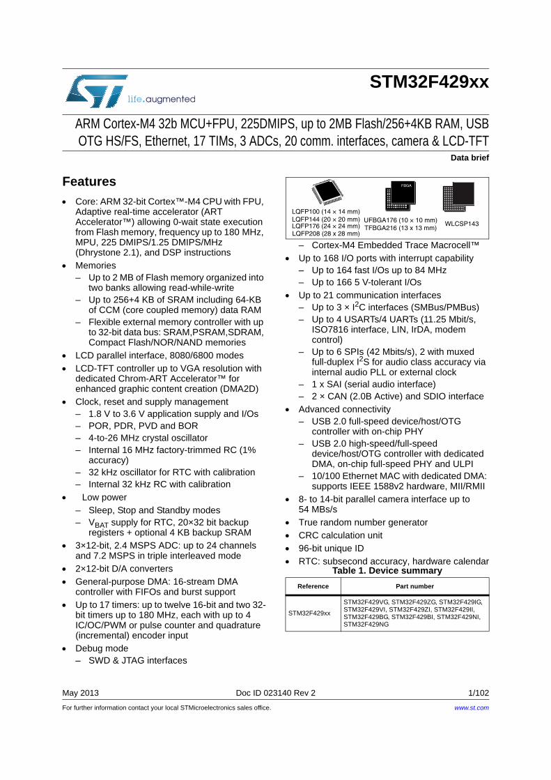
LQFP100 (14 × 14 mm)LQFP144 (20 × 20 mm) UFBGA176 (10 × 10 mm)LQFP176 (24 × 24 mm)LQFP208 (28 x 28 mm)
TFBGA216 (13 x 13 mm)WLCSP143
www.st.com
Contents STM32F429xx
2/102 Doc ID 023140 Rev 2
Contents
1 Introduction . . . . . . . . . . . . . . . . . . . . . . . . . . . . . . . . . . . . . . . . . . . . . . . . 7
2 Description . . . . . . . . . . . . . . . . . . . . . . . . . . . . . . . . . . . . . . . . . . . . . . . . . 82.1 Full compatibility throughout the family . . . . . . . . . . . . . . . . . . . . . . . . . . .11
3 Functional overview . . . . . . . . . . . . . . . . . . . . . . . . . . . . . . . . . . . . . . . . 143.1 ARM® Cortex™-M4 with FPU and embedded Flash and SRAM . . . . . . . 14
3.2 Adaptive real-time memory accelerator (ART Accelerator™) . . . . . . . . . 14
3.3 Memory protection unit . . . . . . . . . . . . . . . . . . . . . . . . . . . . . . . . . . . . . . . 14
3.4 Embedded Flash memory . . . . . . . . . . . . . . . . . . . . . . . . . . . . . . . . . . . . 15
3.5 CRC (cyclic redundancy check) calculation unit . . . . . . . . . . . . . . . . . . . 15
3.6 Embedded SRAM . . . . . . . . . . . . . . . . . . . . . . . . . . . . . . . . . . . . . . . . . . . 15
3.7 Multi-AHB bus matrix . . . . . . . . . . . . . . . . . . . . . . . . . . . . . . . . . . . . . . . . 15
3.8 DMA controller (DMA) . . . . . . . . . . . . . . . . . . . . . . . . . . . . . . . . . . . . . . . 16
3.9 Flexible memory controller (FMC) . . . . . . . . . . . . . . . . . . . . . . . . . . . . . . 17
3.10 LCD-TFT controller . . . . . . . . . . . . . . . . . . . . . . . . . . . . . . . . . . . . . . . . . . 17
3.11 Chrom-ART Accelerator™ (DMA2D) . . . . . . . . . . . . . . . . . . . . . . . . . . . . 18
3.12 Nested vectored interrupt controller (NVIC) . . . . . . . . . . . . . . . . . . . . . . . 18
3.13 External interrupt/event controller (EXTI) . . . . . . . . . . . . . . . . . . . . . . . . . 18
3.14 Clocks and startup . . . . . . . . . . . . . . . . . . . . . . . . . . . . . . . . . . . . . . . . . . 18
3.15 Boot modes . . . . . . . . . . . . . . . . . . . . . . . . . . . . . . . . . . . . . . . . . . . . . . . 19
3.16 Power supply schemes . . . . . . . . . . . . . . . . . . . . . . . . . . . . . . . . . . . . . . 19
3.17 Power supply supervisor . . . . . . . . . . . . . . . . . . . . . . . . . . . . . . . . . . . . . 193.17.1 Internal reset ON . . . . . . . . . . . . . . . . . . . . . . . . . . . . . . . . . . . . . . . . . . 19
3.17.2 Internal reset OFF . . . . . . . . . . . . . . . . . . . . . . . . . . . . . . . . . . . . . . . . . 20
3.18 Voltage regulator . . . . . . . . . . . . . . . . . . . . . . . . . . . . . . . . . . . . . . . . . . . 213.18.1 Regulator ON . . . . . . . . . . . . . . . . . . . . . . . . . . . . . . . . . . . . . . . . . . . . . 21
3.18.2 Regulator OFF . . . . . . . . . . . . . . . . . . . . . . . . . . . . . . . . . . . . . . . . . . . . 22
3.18.3 Regulator ON/OFF and internal reset ON/OFF availability . . . . . . . . . . 25
3.19 Real-time clock (RTC), backup SRAM and backup registers . . . . . . . . . . 25
3.20 Low-power modes . . . . . . . . . . . . . . . . . . . . . . . . . . . . . . . . . . . . . . . . . . 26
3.21 VBAT operation . . . . . . . . . . . . . . . . . . . . . . . . . . . . . . . . . . . . . . . . . . . . . 27
Doc ID 023140 Rev 2 3/102
STM32F429xx Contents
3.22 Timers and watchdogs . . . . . . . . . . . . . . . . . . . . . . . . . . . . . . . . . . . . . . . 273.22.1 Advanced-control timers (TIM1, TIM8) . . . . . . . . . . . . . . . . . . . . . . . . . 28
3.22.2 General-purpose timers (TIMx) . . . . . . . . . . . . . . . . . . . . . . . . . . . . . . . 29
3.22.3 Basic timers TIM6 and TIM7 . . . . . . . . . . . . . . . . . . . . . . . . . . . . . . . . . 29
3.22.4 Independent watchdog . . . . . . . . . . . . . . . . . . . . . . . . . . . . . . . . . . . . . 29
3.22.5 Window watchdog . . . . . . . . . . . . . . . . . . . . . . . . . . . . . . . . . . . . . . . . . 29
3.22.6 SysTick timer . . . . . . . . . . . . . . . . . . . . . . . . . . . . . . . . . . . . . . . . . . . . . 30
3.23 Inter-integrated circuit interface (I2C) . . . . . . . . . . . . . . . . . . . . . . . . . . . . 30
3.24 Universal synchronous/asynchronous receiver transmitters (USART) . . 30
3.25 Serial peripheral interface (SPI) . . . . . . . . . . . . . . . . . . . . . . . . . . . . . . . . 31
3.26 Inter-integrated sound (I2S) . . . . . . . . . . . . . . . . . . . . . . . . . . . . . . . . . . . 31
3.27 Serial Audio interface (SAI1) . . . . . . . . . . . . . . . . . . . . . . . . . . . . . . . . . . 32
3.28 Audio PLL (PLLI2S) . . . . . . . . . . . . . . . . . . . . . . . . . . . . . . . . . . . . . . . . . 32
3.29 Audio and LCD PLL(PLLSAI) . . . . . . . . . . . . . . . . . . . . . . . . . . . . . . . . . . 32
3.30 Secure digital input/output interface (SDIO) . . . . . . . . . . . . . . . . . . . . . . . 32
3.31 Ethernet MAC interface with dedicated DMA and IEEE 1588 support . . . 33
3.32 Controller area network (bxCAN) . . . . . . . . . . . . . . . . . . . . . . . . . . . . . . . 33
3.33 Universal serial bus on-the-go full-speed (OTG_FS) . . . . . . . . . . . . . . . . 34
3.34 Universal serial bus on-the-go high-speed (OTG_HS) . . . . . . . . . . . . . . . 34
3.35 Digital camera interface (DCMI) . . . . . . . . . . . . . . . . . . . . . . . . . . . . . . . . 35
3.36 Random number generator (RNG) . . . . . . . . . . . . . . . . . . . . . . . . . . . . . . 35
3.37 General-purpose input/outputs (GPIOs) . . . . . . . . . . . . . . . . . . . . . . . . . . 35
3.38 Analog-to-digital converters (ADCs) . . . . . . . . . . . . . . . . . . . . . . . . . . . . . 35
3.39 Temperature sensor . . . . . . . . . . . . . . . . . . . . . . . . . . . . . . . . . . . . . . . . . 36
3.40 Digital-to-analog converter (DAC) . . . . . . . . . . . . . . . . . . . . . . . . . . . . . . 36
3.41 Serial wire JTAG debug port (SWJ-DP) . . . . . . . . . . . . . . . . . . . . . . . . . . 36
3.42 Embedded Trace Macrocell™ . . . . . . . . . . . . . . . . . . . . . . . . . . . . . . . . . 36
4 Pinouts and pin description . . . . . . . . . . . . . . . . . . . . . . . . . . . . . . . . . . 38
5 Memory mapping . . . . . . . . . . . . . . . . . . . . . . . . . . . . . . . . . . . . . . . . . . . 76
6 Package characteristics . . . . . . . . . . . . . . . . . . . . . . . . . . . . . . . . . . . . . 816.1 Package mechanical data . . . . . . . . . . . . . . . . . . . . . . . . . . . . . . . . . . . . 81
6.2 Thermal characteristics . . . . . . . . . . . . . . . . . . . . . . . . . . . . . . . . . . . . . . 94
Contents STM32F429xx
4/102 Doc ID 023140 Rev 2
7 Part numbering . . . . . . . . . . . . . . . . . . . . . . . . . . . . . . . . . . . . . . . . . . . . 95
Appendix A Application block diagrams . . . . . . . . . . . . . . . . . . . . . . . . . . . . . . . 96A.1 USB OTG full speed (FS) interface solutions . . . . . . . . . . . . . . . . . . . . . . 96
A.2 USB OTG high speed (HS) interface solutions . . . . . . . . . . . . . . . . . . . . . 98
A.3 Ethernet interface solutions. . . . . . . . . . . . . . . . . . . . . . . . . . . . . . . . . . . . 99
8 Revision history . . . . . . . . . . . . . . . . . . . . . . . . . . . . . . . . . . . . . . . . . . 101

Doc ID 023140 Rev 2 5/102
STM32F429xx List of tables
List of tables
Table 1. Device summary . . . . . . . . . . . . . . . . . . . . . . . . . . . . . . . . . . . . . . . . . . . . . . . . . . . . . . . . . . 1Table 2. STM32F429xx features and peripheral counts . . . . . . . . . . . . . . . . . . . . . . . . . . . . . . . . . . . 9Table 3. Voltage regulator configuration mode versus device operating mode . . . . . . . . . . . . . . . . 22Table 4. Regulator ON/OFF and internal reset ON/OFF availability. . . . . . . . . . . . . . . . . . . . . . . . . 25Table 5. Voltage regulator modes in stop mode . . . . . . . . . . . . . . . . . . . . . . . . . . . . . . . . . . . . . . . . 26Table 6. Timer feature comparison. . . . . . . . . . . . . . . . . . . . . . . . . . . . . . . . . . . . . . . . . . . . . . . . . . 28Table 7. Comparison of I2C analog and digital filters . . . . . . . . . . . . . . . . . . . . . . . . . . . . . . . . . . . . 30Table 8. USART feature comparison . . . . . . . . . . . . . . . . . . . . . . . . . . . . . . . . . . . . . . . . . . . . . . . . 31Table 9. Legend/abbreviations used in the pinout table . . . . . . . . . . . . . . . . . . . . . . . . . . . . . . . . . . 45Table 10. STM32F429xx pin and ball definitions . . . . . . . . . . . . . . . . . . . . . . . . . . . . . . . . . . . . . . . . 46Table 11. FMC pin definition. . . . . . . . . . . . . . . . . . . . . . . . . . . . . . . . . . . . . . . . . . . . . . . . . . . . . . . . 62Table 12. STM32F429xx alternate function mapping . . . . . . . . . . . . . . . . . . . . . . . . . . . . . . . . . . . . . 65Table 13. STM32F429xx register boundary addresses . . . . . . . . . . . . . . . . . . . . . . . . . . . . . . . . . . . 77Table 14. LQPF100, 14 x 14 mm 100-pin low-profile quad flat package mechanical data. . . . . . . . . 82Table 15. WLCSP143, 0.4 mm pitch wafe level chip scale package mechanical data. . . . . . . . . . . . 85Table 16. LQFP144, 20 x 20 mm, 144-pin low-profile quad flat package
mechanical data . . . . . . . . . . . . . . . . . . . . . . . . . . . . . . . . . . . . . . . . . . . . . . . . . . . . . . . . . 86Table 17. LQFP176, 24 x 24 mm, 176-pin low-profile quad flat package
mechanical data . . . . . . . . . . . . . . . . . . . . . . . . . . . . . . . . . . . . . . . . . . . . . . . . . . . . . . . . . 88Table 18. LQFP208, 28 x 28 mm, 208-pin low-profile quad flat package
mechanical data . . . . . . . . . . . . . . . . . . . . . . . . . . . . . . . . . . . . . . . . . . . . . . . . . . . . . . . . . 90Table 19. UFBGA176+25 - ultra thin fine pitch ball grid array 10 × 10 × 0.6 mm
mechanical data . . . . . . . . . . . . . . . . . . . . . . . . . . . . . . . . . . . . . . . . . . . . . . . . . . . . . . . . . 92Table 20. TFBGA216 - ultra thin fine pitch ball grid array 13 × 13 × 0.8mm
package mechanical data . . . . . . . . . . . . . . . . . . . . . . . . . . . . . . . . . . . . . . . . . . . . . . . . . . 93Table 21. Package thermal characteristics . . . . . . . . . . . . . . . . . . . . . . . . . . . . . . . . . . . . . . . . . . . . . 94Table 22. Ordering information scheme . . . . . . . . . . . . . . . . . . . . . . . . . . . . . . . . . . . . . . . . . . . . . . . 95Table 23. Document revision history . . . . . . . . . . . . . . . . . . . . . . . . . . . . . . . . . . . . . . . . . . . . . . . . 101
STM32F429xx
6/102 Doc ID 023140 Rev 2
Figure 1. Compatible board design STM32F10xx/STM32F2xx/STM32F4xxfor LQFP100 package. . . . . . . . . . . . . . . . . . . . . . . . . . . . . . . . . . . . . . . . . . . . . . . . . . . . . 11
Figure 2. Compatible board design between STM32F10xx/STM32F2xx/STM32F4xxfor LQFP144 package. . . . . . . . . . . . . . . . . . . . . . . . . . . . . . . . . . . . . . . . . . . . . . . . . . . . . 12
Figure 3. Compatible board design between STM32F2xx and STM32F4xx for LQFP176 package . . . . . . . . . . . . . . . . . . . . . . . . . . . . . . . . . . . . . . . . . . . . . . . . . . . . 12
Figure 4. STM32F429xx block diagram . . . . . . . . . . . . . . . . . . . . . . . . . . . . . . . . . . . . . . . . . . . . . . 13Figure 5. STM32F429xx Multi-AHB matrix . . . . . . . . . . . . . . . . . . . . . . . . . . . . . . . . . . . . . . . . . . . . 16Figure 6. Power supply supervisor interconnection with internal reset OFF . . . . . . . . . . . . . . . . . . . 20Figure 7. PDR_ON control with internal reset OFF . . . . . . . . . . . . . . . . . . . . . . . . . . . . . . . . . . . . . . 21Figure 8. Regulator OFF . . . . . . . . . . . . . . . . . . . . . . . . . . . . . . . . . . . . . . . . . . . . . . . . . . . . . . . . . . 23Figure 9. Startup in regulator OFF: slow VDD slope
- power-down reset risen after VCAP_1/VCAP_2 stabilization . . . . . . . . . . . . . . . . . . . . . . . . 24Figure 10. Startup in regulator OFF mode: fast VDD slope
- power-down reset risen before VCAP_1/VCAP_2 stabilization . . . . . . . . . . . . . . . . . . . . . . 24Figure 11. STM32F42x LQFP100 pinout . . . . . . . . . . . . . . . . . . . . . . . . . . . . . . . . . . . . . . . . . . . . . . . 38Figure 12. STM32F42x WLCSP143 pinout . . . . . . . . . . . . . . . . . . . . . . . . . . . . . . . . . . . . . . . . . . . . . 39Figure 13. STM32F42x LQFP144 pinout . . . . . . . . . . . . . . . . . . . . . . . . . . . . . . . . . . . . . . . . . . . . . . . 40Figure 14. STM32F42x LQFP176 pinout . . . . . . . . . . . . . . . . . . . . . . . . . . . . . . . . . . . . . . . . . . . . . . . 41Figure 15. STM32F42x LQFP208 pinout . . . . . . . . . . . . . . . . . . . . . . . . . . . . . . . . . . . . . . . . . . . . . . . 42Figure 16. STM32F42x UFBGA176 ballout . . . . . . . . . . . . . . . . . . . . . . . . . . . . . . . . . . . . . . . . . . . . . 43Figure 17. STM32F42x TFBGA216 ballout . . . . . . . . . . . . . . . . . . . . . . . . . . . . . . . . . . . . . . . . . . . . . 44Figure 18. Memory map. . . . . . . . . . . . . . . . . . . . . . . . . . . . . . . . . . . . . . . . . . . . . . . . . . . . . . . . . . . . 76Figure 19. LQFP100, 14 x 14 mm 100-pin low-profile quad flat package outline . . . . . . . . . . . . . . . . 81Figure 20. LQPF100 recommended footprint . . . . . . . . . . . . . . . . . . . . . . . . . . . . . . . . . . . . . . . . . . . 83Figure 21. WLCSP143, 0.4 mm pitch wafe level chip scale package outline . . . . . . . . . . . . . . . . . . . 84Figure 22. LQFP144, 20 x 20 mm, 144-pin low-profile quad flat package outline . . . . . . . . . . . . . . . . 86Figure 23. LQFP144 recommended footprint . . . . . . . . . . . . . . . . . . . . . . . . . . . . . . . . . . . . . . . . . . . 87Figure 24. LQFP176 24 x 24 mm, 176-pin low-profile quad flat package outline . . . . . . . . . . . . . . . . 88Figure 25. LQFP176 recommended footprint . . . . . . . . . . . . . . . . . . . . . . . . . . . . . . . . . . . . . . . . . . . 89Figure 26. LQFP208, 28 x 28 mm, 208-pin low-profile quad flat package outline . . . . . . . . . . . . . . . . 90Figure 27. LQFP208 recommended footprint . . . . . . . . . . . . . . . . . . . . . . . . . . . . . . . . . . . . . . . . . . . 91Figure 28. UFBGA176+25 - ultra thin fine pitch ball grid array 10 × 10 × 0.6 mm,
package outline. . . . . . . . . . . . . . . . . . . . . . . . . . . . . . . . . . . . . . . . . . . . . . . . . . . . . . . . . . 92Figure 29. TFBGA216 - ultra thin fine pitch ball grid array 13 × 13 × 0.8mm,
package outline. . . . . . . . . . . . . . . . . . . . . . . . . . . . . . . . . . . . . . . . . . . . . . . . . . . . . . . . . . 93Figure 30. USB controller configured as peripheral-only and used
in Full speed mode . . . . . . . . . . . . . . . . . . . . . . . . . . . . . . . . . . . . . . . . . . . . . . . . . . . . . . . 96Figure 31. USB controller configured as host-only and used in full speed mode. . . . . . . . . . . . . . . . . 96Figure 32. USB controller configured in dual mode and used in full speed mode . . . . . . . . . . . . . . . . 97Figure 33. USB controller configured as peripheral, host, or dual-mode
and used in high speed mode. . . . . . . . . . . . . . . . . . . . . . . . . . . . . . . . . . . . . . . . . . . . . . . 98Figure 34. MII mode using a 25 MHz crystal . . . . . . . . . . . . . . . . . . . . . . . . . . . . . . . . . . . . . . . . . . . . 99Figure 35. RMII with a 50 MHz oscillator . . . . . . . . . . . . . . . . . . . . . . . . . . . . . . . . . . . . . . . . . . . . . . . 99Figure 36. RMII with a 25 MHz crystal and PHY with PLL. . . . . . . . . . . . . . . . . . . . . . . . . . . . . . . . . 100
Doc ID 023140 Rev 2 7/102
STM32F429xx Introduction
1 Introduction
This databrief provides the description of the STM32F429xx line of microcontrollers. For more details on the whole STMicroelectronics STM32™ family, please refer to Section 2.1: Full compatibility throughout the family.
The STM32F429xx databrief should be read in conjunction with the STM32F4xx reference manual.
For information on the Cortex™-M4 core, please refer to the Cortex™-M4 programming manual (PM0214), available from the www.arm.com.
Description STM32F429xx
8/102 Doc ID 023140 Rev 2
2 Description
The STM32F429XX devices is based on the high-performance ARM® Cortex™-M4 32-bit RISC core operating at a frequency of up to 180 MHz. The Cortex-M4 core features a Floating point unit (FPU) single precision which supports all ARM single-precision data-processing instructions and data types. It also implements a full set of DSP instructions and a memory protection unit (MPU) which enhances application security.
The STM32F429xx devices incorporates high-speed embedded memories (Flash memory up to 2 Mbyte, up to 256 Kbytes of SRAM), up to 4 Kbytes of backup SRAM, and an extensive range of enhanced I/Os and peripherals connected to two APB buses, two AHB buses and a 32-bit multi-AHB bus matrix.
All devices offer three 12-bit ADCs, two DACs, a low-power RTC, twelve general-purpose 16-bit timers including two PWM timers for motor control, two general-purpose 32-bit timers. a true random number generator (RNG). They also feature standard and advanced communication interfaces. • Up to three I2Cs• Six SPIs, two I2Ss full duplex. To achieve audio class accuracy, the I2S peripherals can
be clocked via a dedicated internal audio PLL or via an external clock to allow synchronization.
• Four USARTs plus four UARTs• An USB OTG full-speed and a USB OTG high-speed with full-speed capability (with the
ULPI), • Two CANs• One SAI serial audio interface• An SDIO/MMC interface• Ethernet and the camera interface• LCD-TFT display controller• DMA2D controller.
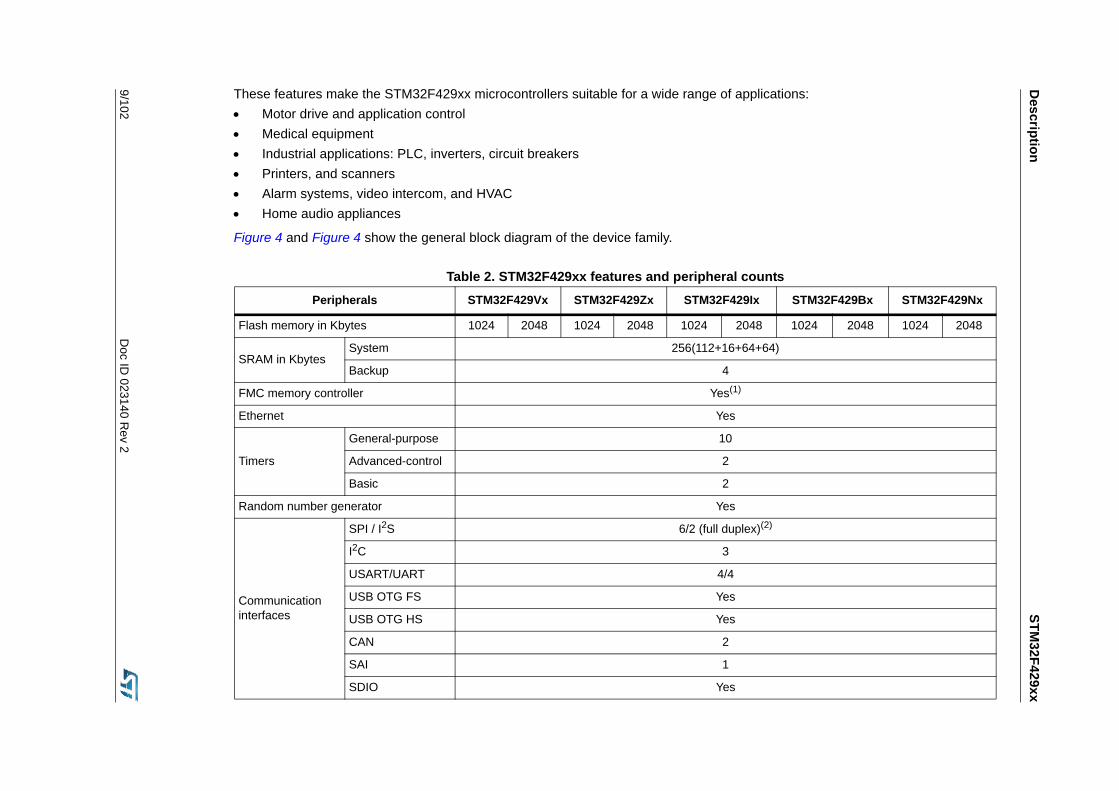
Advanced peripherals include an SDIO, a flexible memory control (FMC) interface, a camera interface for CMOS sensors. Refer to Table 2: STM32F429xx features and peripheral counts for the list of peripherals available on each part number.
The STM32F429xx devices operates in the –40 to +105 °C temperature range from a 1.8 to 3.6 V power supply.
The supply voltage can drop to 1.7 V when the device operates in the 0 to 70 °C temperature range with the use of an external power supply supervisor (refer to Section 3.17.2: Internal reset OFF). A comprehensive set of power-saving mode allows the design of low-power applications.
The STM32F429xx devices offers devices in 7 packages ranging from 100 pins to 216 pins. The set of included peripherals changes with the device chosen.
Description
STM32F429xx
9/102D
oc ID 023140 R
ev 2
These features make the STM32F429xx microcontrollers suitable for a wide range of applications:• Motor drive and application control• Medical equipment• Industrial applications: PLC, inverters, circuit breakers• Printers, and scanners• Alarm systems, video intercom, and HVAC• Home audio appliances
Figure 4 and Figure 4 show the general block diagram of the device family.
Table 2. STM32F429xx features and peripheral counts
Peripherals STM32F429Vx STM32F429Zx STM32F429Ix STM32F429Bx STM32F429Nx
Flash memory in Kbytes 1024 2048 1024 2048 1024 2048 1024 2048 1024 2048
SRAM in KbytesSystem 256(112+16+64+64)
Backup 4
FMC memory controller Yes(1)
Ethernet Yes
Timers
General-purpose 10
Advanced-control 2
Basic 2
Random number generator Yes
Communication interfaces
SPI / I2S 6/2 (full duplex)(2)
I2C 3
USART/UART 4/4
USB OTG FS Yes
USB OTG HS Yes
CAN 2
SAI 1
SDIO Yes
STM32F429xx
Description
Doc ID
023140 Rev 2
10/102
Camera interface Yes
LCD-TFT Yes
Chrom-ART Accelerator™ (DMA2D) Yes
GPIOs 82 114 140 168
12-bit ADCNumber of channels
3
16 24 24
12-bit DACNumber of channels
Yes2
Maximum CPU frequency 180 MHz
Operating voltage 1.8 to 3.6 V(3)
Operating temperaturesAmbient temperatures: –40 to +85 °C /–40 to +105 °C
Junction temperature: –40 to + 125 °C
Packages LQFP100WLCSP143LQFP144
UFBGA176LQFP176 LQFP208 TFBGA216
1. For the LQFP100 package, only FMC Bank1 or Bank2 are available. Bank1 can only support a multiplexed NOR/PSRAM memory using the NE1 Chip Select. Bank2 can only support a 16- or 8-bit NAND Flash memory using the NCE2 Chip Select. The interrupt line cannot be used since Port G is not available in this package.
2. The SPI2 and SPI3 interfaces give the flexibility to work in an exclusive way in either the SPI mode or the I2S audio mode.
3. VDD/VDDA minimum value of 1.7 V is obtained when the device operates in reduced temperature range, and with the use of an external power supply supervisor (refer to Section 3.17.2: Internal reset OFF).
Table 2. STM32F429xx features and peripheral counts (continued)
Peripherals STM32F429Vx STM32F429Zx STM32F429Ix STM32F429Bx STM32F429Nx
Doc ID 023140 Rev 2 11/102
STM32F429xx Description
2.1 Full compatibility throughout the familyThe STM32F429xx devices are part of the STM32F4 family. They are fully pin-to-pin, software and feature compatible with the STM32F2xx devices, allowing the user to try different memory densities, peripherals, and performances (FPU, higher frequency) for a greater degree of freedom during the development cycle.
The STM32F429xx devices maintain a close compatibility with the whole STM32F10xx family. All functional pins are pin-to-pin compatible. The STM32F429xx, however, are not drop-in replacements for the STM32F10xx devices: the two families do not have the same power scheme, and so their power pins are different. Nonetheless, transition from the STM32F10xx to the STM32F42x family remains simple as only a few pins are impacted.
Figure 1, Figure 2, and Figure 3, give compatible board designs between the STM32F4xx, STM32F2xx, and STM32F10xx families.
Figure 1. Compatible board design STM32F10xx/STM32F2xx/STM32F4xxfor LQFP100 package
Ω
Ω
Description STM32F429xx
12/102 Doc ID 023140 Rev 2
Figure 2. Compatible board design between STM32F10xx/STM32F2xx/STM32F4xxfor LQFP144 package
Figure 3. Compatible board design between STM32F2xx and STM32F4xx for LQFP176 package
ai18487d
31
71
1 36
37
72
73108
144
109
VSS
0 Ω resistor or soldering bridgepresent for the STM32F10xxconfiguration, not present in theSTM32F4xx configuration
106
VSS
30
Two 0 Ω resistors connected to: - VSS for the STM32F10xx
- VDD or signal from external power supply supervisor for the STM32F4xx
VSSVDD
VSS
VSS
143 (PDR_ON)
VSSVDD
VSS for STM32F10xxVDD for STM32F4xx
- VSS, VDD or NC for the STM32F2xx
Signal from external power
supply supervisor
MS31835V1
1 44
45
8889132
176
133
Two 0 Ω resistors connected to: - VSS, VDD or NC for the STM32F2xx- VDD or signal from external power supply supervisor for the STM32F4xx
171 (PDR_ON)
VSSVDD
Signal from external power supply
supervisor
48 - GND for STM32F2xx- BYPASS_REG for STM32F4xx
Doc ID 023140 Rev 2 13/102
STM32F429xx Description
Figure 4. STM32F429xx block diagram
1. The timers connected to APB2 are clocked from TIMxCLK up to 180 MHz, while the timers connected to APB1 are clocked from TIMxCLK either up to 90 MHz or 180 MHz depending on TIMPRE bit configuration in the RCC_DCKCFGR register.
Functional overview STM32F429xx
14/102 Doc ID 023140 Rev 2
3 Functional overview
3.1 ARM® Cortex™-M4 with FPU and embedded Flash and SRAMThe ARM Cortex-M4 with FPU processor is the latest generation of ARM processors for embedded systems. It was developed to provide a low-cost platform that meets the needs of MCU implementation, with a reduced pin count and low-power consumption, while delivering outstanding computational performance and an advanced response to interrupts.
The ARM Cortex-M4 with FPU core is a 32-bit RISC processor that features exceptional code-efficiency, delivering the high-performance expected from an ARM core in the memory size usually associated with 8- and 16-bit devices.
The processor supports a set of DSP instructions which allow efficient signal processing and complex algorithm execution.
Its single precision FPU (floating point unit) speeds up software development by using metalanguage development tools, while avoiding saturation.
The STM32F42x family is compatible with all ARM tools and software.
Figure 4 shows the general block diagram of the STM32F42x family.
Note: Cortex-M4 with FPU core is binary compatible with the Cortex-M3 core.
3.2 Adaptive real-time memory accelerator (ART Accelerator™)The ART Accelerator™ is a memory accelerator which is optimized for STM32 industry-standard ARM® Cortex™-M4 with FPU processors. It balances the inherent performance advantage of the ARM Cortex-M4 with FPU over Flash memory technologies, which normally requires the processor to wait for the Flash memory at higher frequencies.
To release the processor full 225 DMIPS performance at this frequency, the accelerator implements an instruction prefetch queue and branch cache, which increases program execution speed from the 128-bit Flash memory. Based on CoreMark benchmark, the performance achieved thanks to the ART Accelerator is equivalent to 0 wait state program execution from Flash memory at a CPU frequency up to 180 MHz.
3.3 Memory protection unitThe memory protection unit (MPU) is used to manage the CPU accesses to memory to prevent one task to accidentally corrupt the memory or resources used by any other active task. This memory area is organized into up to 8 protected areas that can in turn be divided up into 8 subareas. The protection area sizes are between 32 bytes and the whole 4 gigabytes of addressable memory.
The MPU is especially helpful for applications where some critical or certified code has to be protected against the misbehavior of other tasks. It is usually managed by an RTOS (real-time operating system). If a program accesses a memory location that is prohibited by the MPU, the RTOS can detect it and take action. In an RTOS environment, the kernel can dynamically update the MPU area setting, based on the process to be executed.
Doc ID 023140 Rev 2 15/102
STM32F429xx Functional overview
The MPU is optional and can be bypassed for applications that do not need it.
3.4 Embedded Flash memoryThe devices embed a Flash memory of 1 Mbytes or 2 Mbytes available for storing programs and data.
3.5 CRC (cyclic redundancy check) calculation unitThe CRC (cyclic redundancy check) calculation unit is used to get a CRC code from a 32-bit data word and a fixed generator polynomial.
Among other applications, CRC-based techniques are used to verify data transmission or storage integrity. In the scope of the EN/IEC 60335-1 standard, they offer a means of verifying the Flash memory integrity. The CRC calculation unit helps compute a software signature during runtime, to be compared with a reference signature generated at link-time and stored at a given memory location.
3.6 Embedded SRAMAll devices embed:• Up to 256 Kbytes of system SRAM including 64 Kbytes of CCM (core coupled memory)
data RAMRAM memory is accessed (read/write) at CPU clock speed with 0 wait states.
• 4 Kbytes of backup SRAM This area is accessible only from the CPU. Its content is protected against possible unwanted write accesses, and is retained in Standby or VBAT mode.
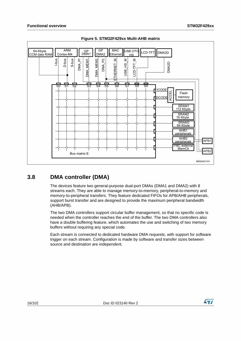
3.7 Multi-AHB bus matrixThe 32-bit multi-AHB bus matrix interconnects all the masters (CPU, DMAs, Ethernet, USB HS, the LCD-TFT, and the DMA2D) and the slaves (Flash memory, RAM, FMC, AHB and APB peripherals) and ensures a seamless and efficient operation even when several high-speed peripherals work simultaneously.
Functional overview STM32F429xx
16/102 Doc ID 023140 Rev 2
Figure 5. STM32F429xx Multi-AHB matrix
3.8 DMA controller (DMA)The devices feature two general-purpose dual-port DMAs (DMA1 and DMA2) with 8 streams each. They are able to manage memory-to-memory, peripheral-to-memory and memory-to-peripheral transfers. They feature dedicated FIFOs for APB/AHB peripherals, support burst transfer and are designed to provide the maximum peripheral bandwidth (AHB/APB).
The two DMA controllers support circular buffer management, so that no specific code is needed when the controller reaches the end of the buffer. The two DMA controllers also have a double buffering feature, which automates the use and switching of two memory buffers without requiring any special code.
Each stream is connected to dedicated hardware DMA requests, with support for software trigger on each stream. Configuration is made by software and transfer sizes between source and destination are independent.
ARMCortex-M4
GPDMA1
GPDMA2
MACEthernet
USB OTGHS
Bus matrix-S
S0 S1 S2 S3 S4 S5 S6 S7ICODE
DCODE
AC
CE
L
Flashmemory
SRAM1 112 Kbyte
SRAM216 Kbyte
AHB1peripherals
AHB2peripherals
FMC externalMemCtl
I-bus
D-b
us
S-b
us
DM
A_P
I
DM
A_M
EM
1
DM
A_M
EM
2
DM
A_P
2
ETH
ER
NE
T_M
US
B_H
S_M
CCM data RAM 64-Kbyte
APB1
APB2
SRAM3 64 Kbyte
LCD-TFT DMA2D
S8 S9
LCD
-TFT
_M
DM
A2D
Doc ID 023140 Rev 2 17/102
STM32F429xx Functional overview
The DMA can be used with the main peripherals: • SPI and I2S• I2C• USART• General-purpose, basic and advanced-control timers TIMx• DAC• SDIO• Camera interface (DCMI)• ADC• SAI1.
3.9 Flexible memory controller (FMC)All devices embed an FMC. It has four Chip Select outputs supporting the following modes: PCCard/Compact Flash, SDRAM, SRAM, PSRAM, NOR Flash and NAND Flash.
Functionality overview:• 8-,16-, 32-bit data bus width• Read FIFO for SDRAM controller• Write FIFO• Maximum FMC_CLK/FMC_SDCLK frequency for synchronous accesses is 90 MHz.
LCD parallel interface
The FMC can be configured to interface seamlessly with most graphic LCD controllers. It supports the Intel 8080 and Motorola 6800 modes, and is flexible enough to adapt to specific LCD interfaces. This LCD parallel interface capability makes it easy to build cost-effective graphic applications using LCD modules with embedded controllers or high performance solutions using external controllers with dedicated acceleration.
3.10 LCD-TFT controllerThe LCD-TFT display controller provides a 24-bit parallel digital RGB (Red, Green, Blue) and delivers all signals to interface directly to a broad range of LCD and TFT panels up to SVGA (800x600) resolution with the following features:• 2 displays layers with dedicated FIFO (64x32-bit)• Color Look-Up table (CLUT) up to 256 colors (256x24-bit) per layer• Up to 8 Input color formats selectable per layer• Flexible blending between two layers using alpha value (per pixel or constant)• Flexible programmable parameters for each layer • Color keying (transparency color)• Up to 4 programmable interrupt events.
Functional overview STM32F429xx
18/102 Doc ID 023140 Rev 2
3.11 Chrom-ART Accelerator™ (DMA2D)The Chrom-Art Accelerator™ (DMA2D) is a graphic accelerator which offers advanced bit blitting, row data copy and pixel format conversion. It supports the following functions:• Rectangle filling with a fixed color• Rectangle copy• Rectangle copy with pixel format conversion• Rectangle composition with blending and pixel format conversion.
Various image format coding are supported, from indirect 4bpp color mode up to 32bpp direct color. It embeds dedicated memory to store color lookup tables.
An interrupt can be generated when an operation is complete or at a programmed watermark.
All the operations are fully automatized and are running independently from the CPU or the DMAs.
3.12 Nested vectored interrupt controller (NVIC)The devices embed a nested vectored interrupt controller able to manage 16 priority levels, and handle up to 91 maskable interrupt channels plus the 16 interrupt lines of the Cortex™-M4 with FPU core. • Closely coupled NVIC gives low-latency interrupt processing• Interrupt entry vector table address passed directly to the core• Allows early processing of interrupts• Processing of late arriving, higher-priority interrupts• Support tail chaining• Processor state automatically saved• Interrupt entry restored on interrupt exit with no instruction overhead
This hardware block provides flexible interrupt management features with minimum interrupt latency.
3.13 External interrupt/event controller (EXTI)The external interrupt/event controller consists of 23 edge-detector lines used to generate interrupt/event requests. Each line can be independently configured to select the trigger event (rising edge, falling edge, both) and can be masked independently. A pending register maintains the status of the interrupt requests. The EXTI can detect an external line with a pulse width shorter than the Internal APB2 clock period. Up to 168 GPIOs can be connected to the 16 external interrupt lines.
3.14 Clocks and startupOn reset the 16 MHz internal RC oscillator is selected as the default CPU clock. The 16 MHz internal RC oscillator is factory-trimmed to offer 1% accuracy over the full temperature range. The application can then select as system clock either the RC oscillator or an external 4-26 MHz clock source. This clock can be monitored for failure. If a failure is
Doc ID 023140 Rev 2 19/102
STM32F429xx Functional overview
detected, the system automatically switches back to the internal RC oscillator and a software interrupt is generated (if enabled). This clock source is input to a PLL thus allowing to increase the frequency up to 180 MHz. Similarly, full interrupt management of the PLL clock entry is available when necessary (for example if an indirectly used external oscillator fails).
Several prescalers allow the configuration of the two AHB buses, the high-speed APB (APB2) and the low-speed APB (APB1) domains. The maximum frequency of the two AHB buses is 180 MHz while the maximum frequency of the high-speed APB domains is 90 MHz. The maximum allowed frequency of the low-speed APB domain is 45 MHz.
The devices embed a dedicated PLL (PLLI2S) and PLLSAI which allows to achieve audio class performance. In this case, the I2S master clock can generate all standard sampling frequencies from 8 kHz to 192 kHz.
3.15 Boot modesAt startup, boot pins are used to select one out of three boot options:• Boot from user Flash• Boot from system memory• Boot from embedded SRAM
The boot loader is located in system memory. It is used to reprogram the Flash memory by using USART1 (PA9/PA10), USART3 (PC10/PC11 or PB10/PB11), CAN2 (PB5/PB13), USB OTG FS in Device mode (PA11/PA12) through DFU (device firmware upgrade).
3.16 Power supply schemes• VDD = 1.8 to 3.6 V: external power supply for I/Os and the internal regulator (when
enabled), provided externally through VDD pins. • VSSA, VDDA = 1.8 to 3.6 V: external analog power supplies for ADC, DAC, Reset
blocks, RCs and PLL. VDDA and VSSA must be connected to VDD and VSS, respectively.• VBAT = 1.65 to 3.6 V: power supply for RTC, external clock 32 kHz oscillator and
backup registers (through power switch) when VDD is not present.
Note: VDD/VDDA minimum value of 1.7 V is obtained when the device operates in reduced temperature range, and with the use of an external power supply supervisor (refer to Section 3.17.2: Internal reset OFF). Refer to Table 3: Voltage regulator configuration mode versus device operating mode to identify the packages supporting this option.
3.17 Power supply supervisor
3.17.1 Internal reset ONOn packages embedding the PDR_ON pin, the power supply supervisor is enabled by holding PDR_ON high. On the other package, the power supply supervisor is always enabled.
The device has an integrated power-on reset (POR)/ power-down reset (PDR) circuitry coupled with a Brownout reset (BOR) circuitry. At power-on, POR/PDR is always active and
Functional overview STM32F429xx
20/102 Doc ID 023140 Rev 2
ensures proper operation starting from 1.8 V. After the 1.8 V POR threshold level is reached, the option byte loading process starts, either to confirm or modify default BOR thresholds, or to disable BOR permanently. Three BOR thresholds are available through option bytes. The device remains in reset mode when VDD is below a specified threshold, VPOR/PDR or VBOR, without the need for an external reset circuit.
The device also features an embedded programmable voltage detector (PVD) that monitors the VDD/VDDA power supply and compares it to the VPVD threshold. An interrupt can be generated when VDD/VDDA drops below the VPVD threshold and/or when VDD/VDDA is higher than the VPVD threshold. The interrupt service routine can then generate a warning message and/or put the MCU into a safe state. The PVD is enabled by software.
3.17.2 Internal reset OFFThis feature is available only on packages featuring the PDR_ON pin. The internal power-on reset (POR) / power-down reset (PDR) circuitry is disabled through the PDR_ON pin.
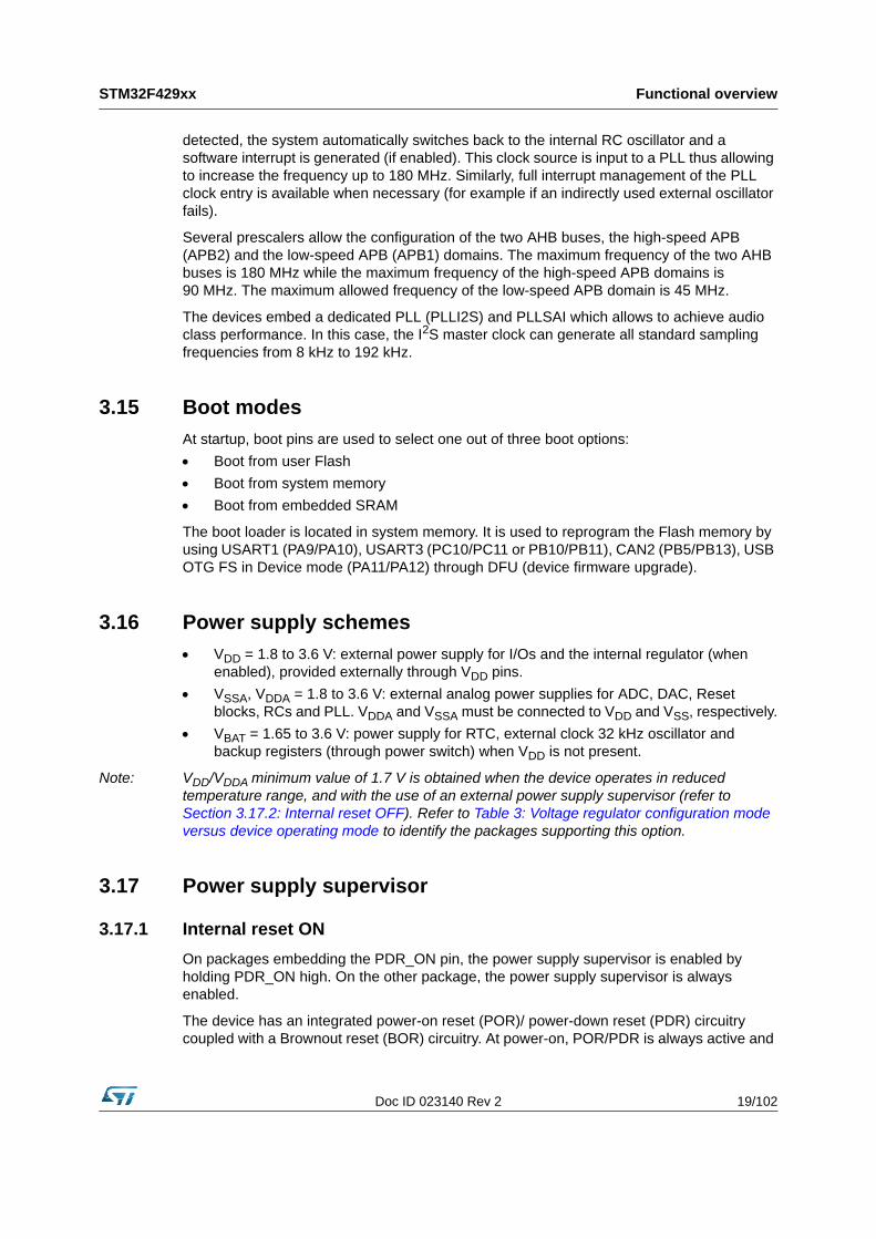
An external power supply supervisor should monitor VDD and should maintain the device in reset mode as long as VDD is below a specified threshold. PDR_ON should be connected to this external power supply supervisor. Refer to Figure 6: Power supply supervisor interconnection with internal reset OFF.
Figure 6. Power supply supervisor interconnection with internal reset OFF
1. PDR = 1.7 V for reduce temperature range; PDR = 1.8 V for all temperature range.
The VDD specified threshold, below which the device must be maintained under reset, is 1.8 V (see Figure 7). This supply voltage can drop to 1.7 V when the device operates in the 0 to 70 °C temperature range.
A comprehensive set of power-saving mode allows to design low-power applications.
When the internal reset is OFF, the following integrated features are no more supported:• The integrated power-on reset (POR) / power-down reset (PDR) circuitry is disabled• The brownout reset (BOR) circuitry must be disabled• The embedded programmable voltage detector (PVD) is disabled• VBAT functionality is no more available and VBAT pin should be connected to VDD.
MS31383V3
NRST
VDD
PDR_ON
External VDD power supply supervisor
Ext. reset controller active whenVDD < 1.7 V or 1.8 V (1)
VDD
Application resetsignal (optional)

Doc ID 023140 Rev 2 21/102
STM32F429xx Functional overview
All packages, except for the LQFP100, allow to disable the internal reset through the PDR_ON signal.
Figure 7. PDR_ON control with internal reset OFF
1. PDR = 1.7 V for reduce temperature range; PDR = 1.8 V for all temperature range.
3.18 Voltage regulatorThe regulator has four operating modes: • Regulator ON
– Main regulator mode (MR)– Low power regulator (LPR)– Power-down
• Regulator OFF
3.18.1 Regulator ONOn packages embedding the BYPASS_REG pin, the regulator is enabled by holding BYPASS_REG low. On all other packages, the regulator is always enabled.
There are three power modes configured by software when the regulator is ON: • MR mode used in Run/sleep modes or in Stop modes
– In Run/Sleep modeThe MR mode is used either in the normal mode (default mode) or the over-drive mode (enabled by software). Different voltages scaling are provided to reach the best compromise between maximum frequency and dynamic power consumption.
MS19009V6
VDD
time
PDR = 1.7 V or 1.8 V (1)
time
NRST
PDR_ON PDR_ON
Reset by other source than power supply supervisor
Functional overview STM32F429xx
22/102 Doc ID 023140 Rev 2
The over-drive mode allows operating at a higher frequency than the normal mode for a given voltage scaling.
– In Stop modesThe MR can be configured in three ways during stop mode: MR operates in normal leakage mode (default mode of MR in stop mode) MR operates in low voltage modeMR operates in under-drive mode (reduced leakage mode).
• LPR is used in the Stop modes:The LP regulator mode is configured by software when entering Stop mode.Like the MR mode, the LPR can be configured in three ways during stop mode:– LPR operates in normal leakage mode (default mode when LPR is ON)– LPR operates in low voltage mode – LPR operates in under-drive mode (reduced leakage mode).
• Power-down is used in Standby mode.The Power-down mode is activated only when entering in Standby mode. The regulator output is in high impedance and the kernel circuitry is powered down, inducing zero consumption. The contents of the registers and SRAM are lost.
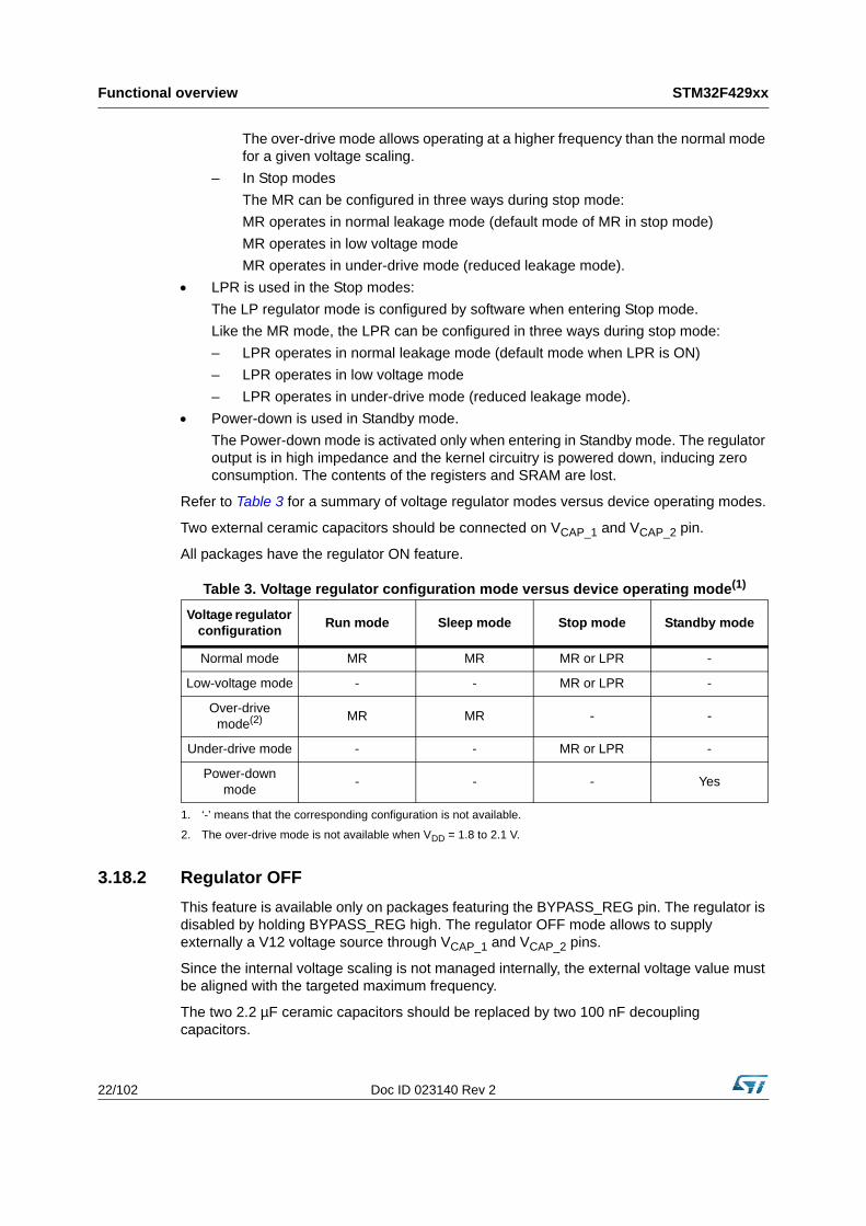
Refer to Table 3 for a summary of voltage regulator modes versus device operating modes.
Two external ceramic capacitors should be connected on VCAP_1 and VCAP_2 pin.
All packages have the regulator ON feature.
3.18.2 Regulator OFFThis feature is available only on packages featuring the BYPASS_REG pin. The regulator is disabled by holding BYPASS_REG high. The regulator OFF mode allows to supply externally a V12 voltage source through VCAP_1 and VCAP_2 pins.
Since the internal voltage scaling is not managed internally, the external voltage value must be aligned with the targeted maximum frequency.
The two 2.2 µF ceramic capacitors should be replaced by two 100 nF decoupling capacitors.
Table 3. Voltage regulator configuration mode versus device operating mode(1)
1. ‘-’ means that the corresponding configuration is not available.
Voltage regulator configuration Run mode Sleep mode Stop mode Standby mode
Normal mode MR MR MR or LPR -
Low-voltage mode - - MR or LPR -
Over-drive mode(2)
2. The over-drive mode is not available when VDD = 1.8 to 2.1 V.
MR MR - -
Under-drive mode - - MR or LPR -
Power-down mode - - - Yes
Doc ID 023140 Rev 2 23/102
STM32F429xx Functional overview
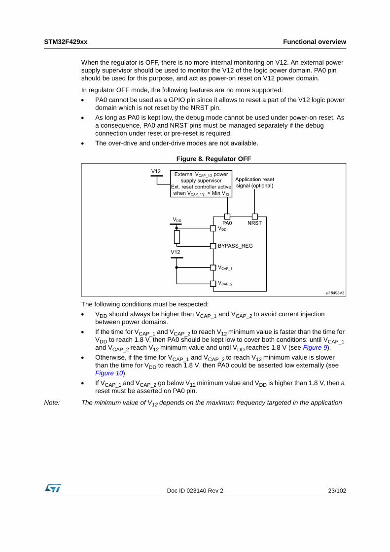
When the regulator is OFF, there is no more internal monitoring on V12. An external power supply supervisor should be used to monitor the V12 of the logic power domain. PA0 pin should be used for this purpose, and act as power-on reset on V12 power domain.
In regulator OFF mode, the following features are no more supported:• PA0 cannot be used as a GPIO pin since it allows to reset a part of the V12 logic power
domain which is not reset by the NRST pin.• As long as PA0 is kept low, the debug mode cannot be used under power-on reset. As
a consequence, PA0 and NRST pins must be managed separately if the debug connection under reset or pre-reset is required.
• The over-drive and under-drive modes are not available.
Figure 8. Regulator OFF
The following conditions must be respected:• VDD should always be higher than VCAP_1 and VCAP_2 to avoid current injection
between power domains. • If the time for VCAP_1 and VCAP_2 to reach V12 minimum value is faster than the time for
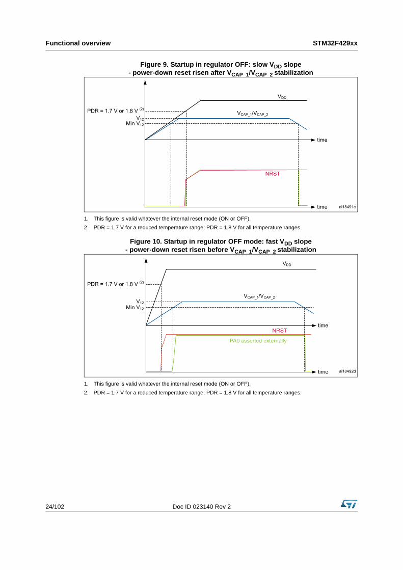
VDD to reach 1.8 V, then PA0 should be kept low to cover both conditions: until VCAP_1 and VCAP_2 reach V12 minimum value and until VDD reaches 1.8 V (see Figure 9).
• Otherwise, if the time for VCAP_1 and VCAP_2 to reach V12 minimum value is slower than the time for VDD to reach 1.8 V, then PA0 could be asserted low externally (see Figure 10).
• If VCAP_1 and VCAP_2 go below V12 minimum value and VDD is higher than 1.8 V, then a reset must be asserted on PA0 pin.
Note: The minimum value of V12 depends on the maximum frequency targeted in the application
ai18498V3
BYPASS_REG
VCAP_1
VCAP_2
PA0
V12
VDD NRST VDD
Application reset signal (optional)
External VCAP_1/2 power supply supervisor
Ext. reset controller active when VCAP_1/2 < Min V12
V12
Functional overview STM32F429xx
24/102 Doc ID 023140 Rev 2
Figure 9. Startup in regulator OFF: slow VDD slope - power-down reset risen after VCAP_1/VCAP_2 stabilization
1. This figure is valid whatever the internal reset mode (ON or OFF). 2. PDR = 1.7 V for a reduced temperature range; PDR = 1.8 V for all temperature ranges.
Figure 10. Startup in regulator OFF mode: fast VDD slope - power-down reset risen before VCAP_1/VCAP_2 stabilization
1. This figure is valid whatever the internal reset mode (ON or OFF). 2. PDR = 1.7 V for a reduced temperature range; PDR = 1.8 V for all temperature ranges.
ai18491e
VDD
time
Min V12
PDR = 1.7 V or 1.8 V (2)VCAP_1/VCAP_2
V12
NRST
time
VDD
time
Min V12
VCAP_1/VCAP_2V12
PA0 asserted externally
NRST
time ai18492d
PDR = 1.7 V or 1.8 V (2)
Doc ID 023140 Rev 2 25/102
STM32F429xx Functional overview
3.18.3 Regulator ON/OFF and internal reset ON/OFF availability
3.19 Real-time clock (RTC), backup SRAM and backup registersThe backup domain includes:• The real-time clock (RTC) • 4 Kbytes of backup SRAM• 20 backup registers
The real-time clock (RTC) is an independent BCD timer/counter. Dedicated registers contain the second, minute, hour (in 12/24 hour), week day, date, month, year, in BCD (binary-coded decimal) format. Correction for 28, 29 (leap year), 30, and 31 day of the month are performed automatically. The RTC provides a programmable alarm and programmable periodic interrupts with wakeup from Stop and Standby modes. The sub-seconds value is also available in binary format.
It is clocked by a 32.768 kHz external crystal, resonator or oscillator, the internal low-power RC oscillator or the high-speed external clock divided by 128. The internal low-speed RC has a typical frequency of 32 kHz. The RTC can be calibrated using an external 512 Hz output to compensate for any natural quartz deviation.
Two alarm registers are used to generate an alarm at a specific time and calendar fields can be independently masked for alarm comparison. To generate a periodic interrupt, a 16-bit programmable binary auto-reload downcounter with programmable resolution is available and allows automatic wakeup and periodic alarms from every 120 µs to every 36 hours.
A 20-bit prescaler is used for the time base clock. It is by default configured to generate a time base of 1 second from a clock at 32.768 kHz.
The 4-Kbyte backup SRAM is an EEPROM-like memory area. It can be used to store data which need to be retained in VBAT and standby mode. This memory area is disabled by default to minimize power consumption (see Section 3.20: Low-power modes). It can be enabled by software.
The backup registers are 32-bit registers used to store 80 bytes of user application data when VDD power is not present. Backup registers are not reset by a system, a power reset, or when the device wakes up from the Standby mode (see Section 3.20: Low-power modes).
Table 4. Regulator ON/OFF and internal reset ON/OFF availability
Package Regulator ON Regulator OFF Internal reset ON Internal reset OFF
LQFP100
Yes No
Yes No
LQFP144
YesPDR_ON set to
VDD
YesPDR_ON
connected to an external power
supply supervisor
WLCSP143, LQFP176, UFBGA176, LQFP208, TFBGA216
Yes BYPASS_REG set
to VSS
YesBYPASS_REG set
to VDD
Functional overview STM32F429xx
26/102 Doc ID 023140 Rev 2
Additional 32-bit registers contain the programmable alarm subseconds, seconds, minutes, hours, day, and date.
Like backup SRAM, the RTC and backup registers are supplied through a switch that is powered either from the VDD supply when present or from the VBAT pin.
3.20 Low-power modesThe devices support three low-power modes to achieve the best compromise between low power consumption, short startup time and available wakeup sources:• Sleep mode
In Sleep mode, only the CPU is stopped. All peripherals continue to operate and can wake up the CPU when an interrupt/event occurs.
• Stop modeThe Stop mode achieves the lowest power consumption while retaining the contents of SRAM and registers. All clocks in the 1.2 V domain are stopped, the PLL, the HSI RC and the HSE crystal oscillators are disabled.The voltage regulator can be put either in main regulator mode (MR) or in low-power mode (LPR). Both modes can be configured as follows (see Table 5: Voltage regulator modes in stop mode): – Normal mode (default mode when MR or LPR is enabled)– Low voltage mode– Under-drive mode.The device can be woken up from the Stop mode by any of the EXTI line (the EXTI line source can be one of the 16 external lines, the PVD output, the RTC alarm / wakeup / tamper / time stamp events, the USB OTG FS/HS wakeup or the Ethernet wakeup).
• Standby modeThe Standby mode is used to achieve the lowest power consumption. The internal voltage regulator is switched off so that the entire 1.2 V domain is powered off. The PLL, the HSI RC and the HSE crystal oscillators are also switched off. After entering Standby mode, the SRAM and register contents are lost except for registers in the backup domain and the backup SRAM when selected.The device exits the Standby mode when an external reset (NRST pin), an IWDG reset, a rising edge on the WKUP pin, or an RTC alarm / wakeup / tamper /time stamp event occurs. The standby mode is not supported when the embedded voltage regulator is bypassed and the 1.2 V domain is controlled by an external power.
Table 5. Voltage regulator modes in stop mode
Voltage regulator configuration Main regulator (MR) Low-power regulator (LPR)
Normal mode MR ON LPR ON
Low-voltage mode MR in low-voltage mode LPR in low-voltage mode
Under-drive mode MR in under-drive mode LPR in under-drive mode
Doc ID 023140 Rev 2 27/102
STM32F429xx Functional overview
Note: When in Standby mode, only an RTC alarm/event or an external reset can wake up the device provided VDD is supplied by an external battery.
3.21 VBAT operationThe VBAT pin allows to power the device VBAT domain from an external battery, an external supercapacitor, or from VDD when no external battery and an external supercapacitor are present.
VBAT operation is activated when VDD is not present.
The VBAT pin supplies the RTC, the backup registers and the backup SRAM.
Note: When the microcontroller is supplied from VBAT, external interrupts and RTC alarm/events do not exit it from VBAT operation. When PDR_ON pin is not connected to VDD (Internal Reset OFF), the VBAT functionality is no more available and VBAT pin should be connected to VDD.
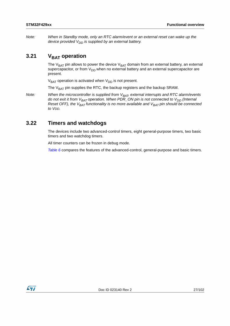
3.22 Timers and watchdogsThe devices include two advanced-control timers, eight general-purpose timers, two basic timers and two watchdog timers.
All timer counters can be frozen in debug mode.
Table 6 compares the features of the advanced-control, general-purpose and basic timers.
Functional overview STM32F429xx
28/102 Doc ID 023140 Rev 2
3.22.1 Advanced-control timers (TIM1, TIM8)The advanced-control timers (TIM1, TIM8) can be seen as three-phase PWM generators multiplexed on 6 channels. They have complementary PWM outputs with programmable inserted dead times. They can also be considered as complete general-purpose timers. Their 4 independent channels can be used for:• Input capture• Output compare• PWM generation (edge- or center-aligned modes)• One-pulse mode output
If configured as standard 16-bit timers, they have the same features as the general-purpose TIMx timers. If configured as 16-bit PWM generators, they have full modulation capability (0-100%).
Table 6. Timer feature comparison
Timer type Timer
Counter resolutio
n
Counter type
Prescaler factor
DMA request
generation
Capture/compare channels
Complementary output
Max interface
clock (MHz)
Max timer clock (MHz)
(1)
Advanced-control
TIM1, TIM8 16-bit
Up, Down, Up/dow
n
Any integer between 1 and 65536
Yes 4 Yes 90 180
General purpose
TIM2, TIM5 32-bit
Up, Down, Up/dow
n
Any integer between 1 and 65536
Yes 4 No 45 90/180
TIM3, TIM4 16-bit
Up, Down, Up/dow
n
Any integer between 1 and 65536
Yes 4 No 45 90/180
TIM9 16-bit UpAny integer between 1 and 65536
No 2 No 90 180
TIM10,
TIM1116-bit Up
Any integer between 1 and 65536
No 1 No 90 180
TIM12 16-bit UpAny integer between 1 and 65536
No 2 No 45 90/180
TIM13,
TIM1416-bit Up
Any integer between 1 and 65536
No 1 No 45 90/180
Basic TIM6, TIM7 16-bit Up
Any integer between 1 and 65536
Yes 0 No 45 90/180
1. The maximum timer clock is either 90 or 180 MHz depending on TIMPRE bit configuration in the RCC_DCKCFGR register.

Doc ID 023140 Rev 2 29/102
STM32F429xx Functional overview
The advanced-control timer can work together with the TIMx timers via the Timer Link feature for synchronization or event chaining.
TIM1 and TIM8 support independent DMA request generation.
3.22.2 General-purpose timers (TIMx)There are ten synchronizable general-purpose timers embedded in the STM32F42x devices (see Table 6 for differences).• TIM2, TIM3, TIM4, TIM5
The STM32F42x include 4 full-featured general-purpose timers: TIM2, TIM5, TIM3, and TIM4.The TIM2 and TIM5 timers are based on a 32-bit auto-reload up/downcounter and a 16-bit prescaler. The TIM3 and TIM4 timers are based on a 16-bit auto-reload up/downcounter and a 16-bit prescaler. They all feature 4 independent channels for input capture/output compare, PWM or one-pulse mode output. This gives up to 16 input capture/output compare/PWMs on the largest packages.The TIM2, TIM3, TIM4, TIM5 general-purpose timers can work together, or with the other general-purpose timers and the advanced-control timers TIM1 and TIM8 via the Timer Link feature for synchronization or event chaining.Any of these general-purpose timers can be used to generate PWM outputs.TIM2, TIM3, TIM4, TIM5 all have independent DMA request generation. They are capable of handling quadrature (incremental) encoder signals and the digital outputs from 1 to 4 hall-effect sensors.
• TIM9, TIM10, TIM11, TIM12, TIM13, and TIM14These timers are based on a 16-bit auto-reload upcounter and a 16-bit prescaler. TIM10, TIM11, TIM13, and TIM14 feature one independent channel, whereas TIM9 and TIM12 have two independent channels for input capture/output compare, PWM or one-pulse mode output. They can be synchronized with the TIM2, TIM3, TIM4, TIM5 full-featured general-purpose timers. They can also be used as simple time bases.
3.22.3 Basic timers TIM6 and TIM7These timers are mainly used for DAC trigger and waveform generation. They can also be used as a generic 16-bit time base.
TIM6 and TIM7 support independent DMA request generation.
3.22.4 Independent watchdogThe independent watchdog is based on a 12-bit downcounter and 8-bit prescaler. It is clocked from an independent 32 kHz internal RC and as it operates independently from the main clock, it can operate in Stop and Standby modes. It can be used either as a watchdog to reset the device when a problem occurs, or as a free-running timer for application timeout management. It is hardware- or software-configurable through the option bytes.
3.22.5 Window watchdogThe window watchdog is based on a 7-bit downcounter that can be set as free-running. It can be used as a watchdog to reset the device when a problem occurs. It is clocked from the main clock. It has an early warning interrupt capability and the counter can be frozen in debug mode.

Functional overview STM32F429xx
30/102 Doc ID 023140 Rev 2
3.22.6 SysTick timerThis timer is dedicated to real-time operating systems, but could also be used as a standard downcounter. It features:• A 24-bit downcounter• Autoreload capability• Maskable system interrupt generation when the counter reaches 0• Programmable clock source.
3.23 Inter-integrated circuit interface (I2C) Up to three I²C bus interfaces can operate in multimaster and slave modes. They can support the standard (up to 100 KHz) and fast (up to 400 KHz) modes. They support the 7/10-bit addressing mode and the 7-bit dual addressing mode (as slave). A hardware CRC generation/verification is embedded.
They can be served by DMA and they support SMBus 2.0/PMBus.
The devices also include programmable analog and digital noise filters (see Table 7).
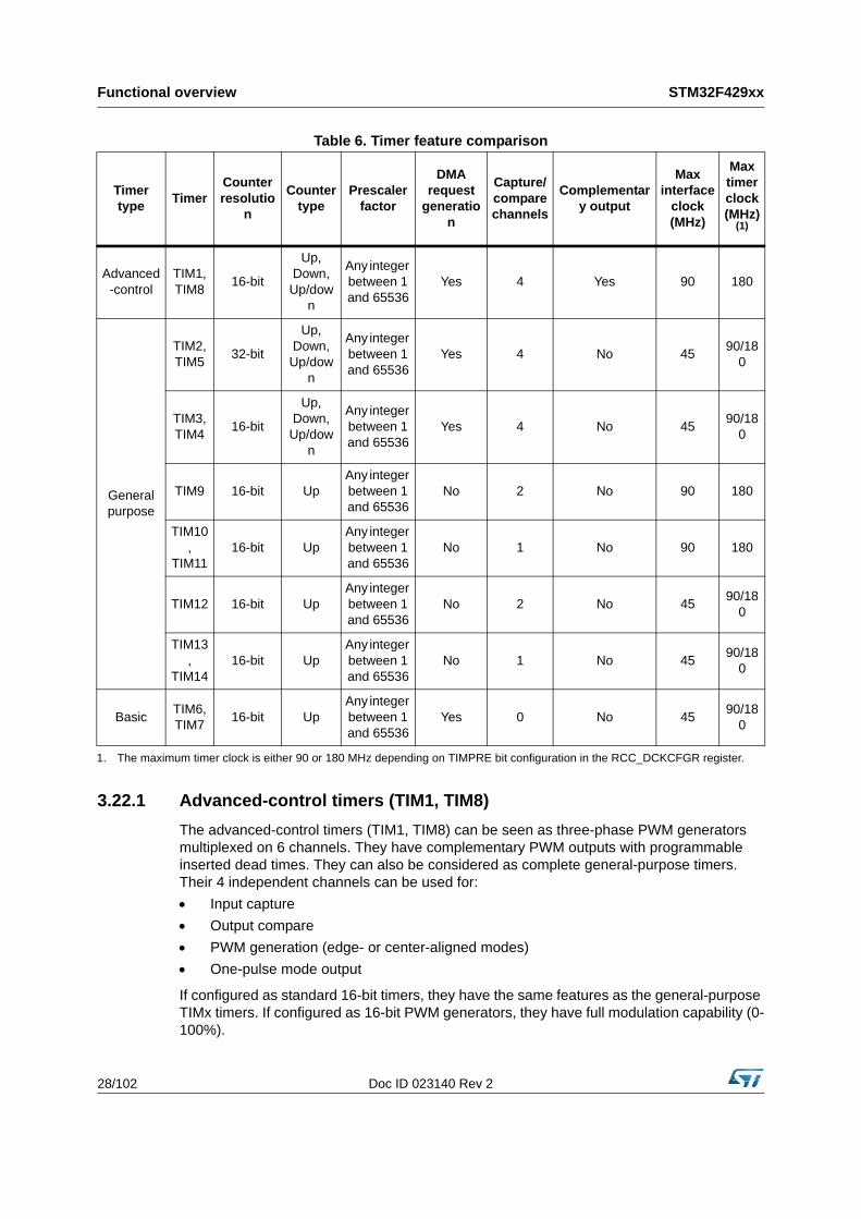
3.24 Universal synchronous/asynchronous receiver transmitters (USART)The devices embed four universal synchronous/asynchronous receiver transmitters (USART1, USART2, USART3 and USART6) and two universal asynchronous receiver transmitters (UART4, UART5, UART7, and UART8).
These six interfaces provide asynchronous communication, IrDA SIR ENDEC support, multiprocessor communication mode, single-wire half-duplex communication mode and have LIN Master/Slave capability. The USART1 and USART6 interfaces are able to communicate at speeds of up to 11.25 Mbit/s. The other available interfaces communicate at up to 5.62 bit/s.
USART1, USART2, USART3 and USART6 also provide hardware management of the CTS and RTS signals, Smart Card mode (ISO 7816 compliant) and SPI-like communication capability. All interfaces can be served by the DMA controller.
Table 7. Comparison of I2C analog and digital filters
Analog filter Digital filter
Pulse width of suppressed spikes ≥ 50 ns Programmable length from 1 to 15
I2C peripheral clocks
Doc ID 023140 Rev 2 31/102
STM32F429xx Functional overview
3.25 Serial peripheral interface (SPI)The devices feature up to six SPIs in slave and master modes in full-duplex and simplex communication modes. SPI1, SPI4, SPI5, and SPI6 can communicate at up to 42 Mbits/s, SPI2 and SPI3 can communicate at up to 21 Mbit/s. The 3-bit prescaler gives 8 master mode frequencies and the frame is configurable to 8 bits or 16 bits. The hardware CRC generation/verification supports basic SD Card/MMC modes. All SPIs can be served by the DMA controller.
The SPI interface can be configured to operate in TI mode for communications in master mode and slave mode.
3.26 Inter-integrated sound (I2S)Two standard I2S interfaces (multiplexed with SPI2 and SPI3) are available. They can be operated in master or slave mode, in full duplex and simplex communication modes, and can be configured to operate with a 16-/32-bit resolution as an input or output channel.
Table 8. USART feature comparison(1)
USART name
Standard
features
Modem (RTS/CT
S)LIN
SPI maste
rirDA Smartcard
(ISO 7816)
Max. baud rate in Mbit/s
(oversampling by 16)
Max. baud rate in Mbit/s
(oversampling by 8)
APB mapping
USART1 X X X X X X 5.62 11.25
APB2 (max.
90 MHz)
USART2 X X X X X X 2.81 5.62
APB1 (max.
45 MHz)
USART3 X X X X X X 2.81 5.62
APB1 (max.
45 MHz)
UART4 X - X - X - 2.81 5.62APB1 (max.
45 MHz)
UART5 X - X - X - 2.81 5.62APB1 (max.
45 MHz)
USART6 X X X X X X 5.62 11.25
APB2 (max.
90 MHz)
UART7 X - X - X - 2.81 5.62APB1 (max.
45 MHz)
UART8 X - X - X - 2.81 5.62APB1 (max.
45 MHz)
1. X = feature supported.
Functional overview STM32F429xx
32/102 Doc ID 023140 Rev 2
Audio sampling frequencies from 8 kHz up to 192 kHz are supported. When either or both of the I2S interfaces is/are configured in master mode, the master clock can be output to the external DAC/CODEC at 256 times the sampling frequency.
All I2Sx can be served by the DMA controller.
Note: For I2S2 full-duplex mode, I2S2_CK and I2S2_WS signals can be used only on GPIO Port B and GPIO Port D.
3.27 Serial Audio interface (SAI1)The serial audio interface (SAI1) is based on two independent audio subblocks which can operate as transmitter or receiver with their FIFO. Many audio protocols are supported by each block: I2S standards, LSB or MSB-justified, PCM/DSP, TDM, AC’97 and SPDIF output, supporting audio sampling frequencies from 8 kHz up to 192 kHz. Both subblocks can be configured in master or in slave mode.
In master mode, the master clock can be output to the external DAC/CODEC at 256 times of the sampling frequency.
The two subblocks can be configured in synchronous mode when full-duplex mode is required.
SAI1 can be served by the DMA controller.
3.28 Audio PLL (PLLI2S)The devices feature an additional dedicated PLL for audio I2S and SAI applications. It allows to achieve error-free I2S sampling clock accuracy without compromising on the CPU performance, while using USB peripherals.
The PLLI2S configuration can be modified to manage an I2S/SAI sample rate change without disabling the main PLL (PLL) used for CPU, USB and Ethernet interfaces.
The audio PLL can be programmed with very low error to obtain sampling rates ranging from 8 KHz to 192 KHz.
In addition to the audio PLL, a master clock input pin can be used to synchronize the I2S/SAI flow with an external PLL (or Codec output).
3.29 Audio and LCD PLL(PLLSAI)An additional PLL dedicated to audio and LCD-TFT is used for SAI1 peripheral in case the PLLI2S is programmed to achieve another audio sampling frequency (49.152 MHz or 11.2896 MHz) and the audio application requires both sampling frequencies simultaneously.
The PLLSAI is also used to generate the LCD-TFT clock.
3.30 Secure digital input/output interface (SDIO)An SD/SDIO/MMC host interface is available, that supports MultiMediaCard System Specification Version 4.2 in three different databus modes: 1-bit (default), 4-bit and 8-bit.
Doc ID 023140 Rev 2 33/102
STM32F429xx Functional overview
The interface allows data transfer at up to 48 MHz, and is compliant with the SD Memory Card Specification Version 2.0.
The SDIO Card Specification Version 2.0 is also supported with two different databus modes: 1-bit (default) and 4-bit.
The current version supports only one SD/SDIO/MMC4.2 card at any one time and a stack of MMC4.1 or previous.
In addition to SD/SDIO/MMC, this interface is fully compliant with the CE-ATA digital protocol Rev1.1.
3.31 Ethernet MAC interface with dedicated DMA and IEEE 1588 supportThe devices provide an IEEE-802.3-2002-compliant media access controller (MAC) for ethernet LAN communications through an industry-standard medium-independent interface (MII) or a reduced medium-independent interface (RMII). The microcontroller requires an external physical interface device (PHY) to connect to the physical LAN bus (twisted-pair, fiber, etc.). The PHY is connected to the device MII port using 17 signals for MII or 9 signals for RMII, and can be clocked using the 25 MHz (MII) from the microcontroller.
The devices include the following features:• Supports 10 and 100 Mbit/s rates• Dedicated DMA controller allowing high-speed transfers between the dedicated SRAM
and the descriptors (see the STM32F4xx reference manual for details)• Tagged MAC frame support (VLAN support)• Half-duplex (CSMA/CD) and full-duplex operation• MAC control sublayer (control frames) support• 32-bit CRC generation and removal• Several address filtering modes for physical and multicast address (multicast and
group addresses)• 32-bit status code for each transmitted or received frame• Internal FIFOs to buffer transmit and receive frames. The transmit FIFO and the
receive FIFO are both 2 Kbytes.• Supports hardware PTP (precision time protocol) in accordance with IEEE 1588 2008
(PTP V2) with the time stamp comparator connected to the TIM2 input• Triggers interrupt when system time becomes greater than target time
3.32 Controller area network (bxCAN)The two CANs are compliant with the 2.0A and B (active) specifications with a bitrate up to 1 Mbit/s. They can receive and transmit standard frames with 11-bit identifiers as well as extended frames with 29-bit identifiers. Each CAN has three transmit mailboxes, two receive FIFOS with 3 stages and 28 shared scalable filter banks (all of them can be used even if one CAN is used). 256 bytes of SRAM are allocated for each CAN.
Functional overview STM32F429xx
34/102 Doc ID 023140 Rev 2
3.33 Universal serial bus on-the-go full-speed (OTG_FS)The devices embed an USB OTG full-speed device/host/OTG peripheral with integrated transceivers. The USB OTG FS peripheral is compliant with the USB 2.0 specification and with the OTG 1.0 specification. It has software-configurable endpoint setting and supports suspend/resume. The USB OTG full-speed controller requires a dedicated 48 MHz clock that is generated by a PLL connected to the HSE oscillator. The major features are:• Combined Rx and Tx FIFO size of 320 × 35 bits with dynamic FIFO sizing• Supports the session request protocol (SRP) and host negotiation protocol (HNP)• 4 bidirectional endpoints• 8 host channels with periodic OUT support• HNP/SNP/IP inside (no need for any external resistor)• For OTG/Host modes, a power switch is needed in case bus-powered devices are
connected
3.34 Universal serial bus on-the-go high-speed (OTG_HS)The devices embed a USB OTG high-speed (up to 480 Mb/s) device/host/OTG peripheral. The USB OTG HS supports both full-speed and high-speed operations. It integrates the transceivers for full-speed operation (12 MB/s) and features a UTMI low-pin interface (ULPI) for high-speed operation (480 MB/s). When using the USB OTG HS in HS mode, an external PHY device connected to the ULPI is required.
The USB OTG HS peripheral is compliant with the USB 2.0 specification and with the OTG 1.0 specification. It has software-configurable endpoint setting and supports suspend/resume. The USB OTG full-speed controller requires a dedicated 48 MHz clock that is generated by a PLL connected to the HSE oscillator.
The major features are:• Combined Rx and Tx FIFO size of 1 Kbit × 35 with dynamic FIFO sizing• Supports the session request protocol (SRP) and host negotiation protocol (HNP)• 6 bidirectional endpoints• 12 host channels with periodic OUT support• Internal FS OTG PHY support • External HS or HS OTG operation supporting ULPI in SDR mode. The OTG PHY is
connected to the microcontroller ULPI port through 12 signals. It can be clocked using the 60 MHz output.
• Internal USB DMA• HNP/SNP/IP inside (no need for any external resistor)• for OTG/Host modes, a power switch is needed in case bus-powered devices are
connected
Doc ID 023140 Rev 2 35/102
STM32F429xx Functional overview
3.35 Digital camera interface (DCMI)The devices embed a camera interface that can connect with camera modules and CMOS sensors through an 8-bit to 14-bit parallel interface, to receive video data. The camera interface can sustain a data transfer rate up to 54 Mbyte/s at 54 MHz. It features:• Programmable polarity for the input pixel clock and synchronization signals• Parallel data communication can be 8-, 10-, 12- or 14-bit• Supports 8-bit progressive video monochrome or raw bayer format, YCbCr 4:2:2
progressive video, RGB 565 progressive video or compressed data (like JPEG)• Supports continuous mode or snapshot (a single frame) mode• Capability to automatically crop the image
3.36 Random number generator (RNG)All devices embed an RNG that delivers 32-bit random numbers generated by an integrated analog circuit.
3.37 General-purpose input/outputs (GPIOs)Each of the GPIO pins can be configured by software as output (push-pull or open-drain, with or without pull-up or pull-down), as input (floating, with or without pull-up or pull-down) or as peripheral alternate function. Most of the GPIO pins are shared with digital or analog alternate functions. All GPIOs are high-current-capable and have speed selection to better manage internal noise, power consumption and electromagnetic emission.
The I/O configuration can be locked if needed by following a specific sequence in order to avoid spurious writing to the I/Os registers.
Fast I/O handling allowing maximum I/O toggling up to 84 MHz.
3.38 Analog-to-digital converters (ADCs)Three 12-bit analog-to-digital converters are embedded and each ADC shares up to 16 external channels, performing conversions in the single-shot or scan mode. In scan mode, automatic conversion is performed on a selected group of analog inputs.
Additional logic functions embedded in the ADC interface allow:• Simultaneous sample and hold• Interleaved sample and hold
The ADC can be served by the DMA controller. An analog watchdog feature allows very precise monitoring of the converted voltage of one, some or all selected channels. An interrupt is generated when the converted voltage is outside the programmed thresholds.
To synchronize A/D conversion and timers, the ADCs could be triggered by any of TIM1, TIM2, TIM3, TIM4, TIM5, or TIM8 timer.
Functional overview STM32F429xx
36/102 Doc ID 023140 Rev 2
3.39 Temperature sensorThe temperature sensor has to generate a voltage that varies linearly with temperature. The conversion range is between 1.8 V and 3.6 V. The temperature sensor is internally connected to the same input channel as VBAT, ADC1_IN18, which is used to convert the sensor output voltage into a digital value. When the temperature sensor and VBAT conversion are enabled at the same time, only VBAT conversion is performed.
As the offset of the temperature sensor varies from chip to chip due to process variation, the internal temperature sensor is mainly suitable for applications that detect temperature changes instead of absolute temperatures. If an accurate temperature reading is needed, then an external temperature sensor part should be used.
3.40 Digital-to-analog converter (DAC)The two 12-bit buffered DAC channels can be used to convert two digital signals into two analog voltage signal outputs.
This dual digital Interface supports the following features:• two DAC converters: one for each output channel• 8-bit or 10-bit monotonic output• left or right data alignment in 12-bit mode• synchronized update capability• noise-wave generation• triangular-wave generation• dual DAC channel independent or simultaneous conversions• DMA capability for each channel• external triggers for conversion• input voltage reference VREF+
Eight DAC trigger inputs are used in the device. The DAC channels are triggered through the timer update outputs that are also connected to different DMA streams.
3.41 Serial wire JTAG debug port (SWJ-DP)The ARM SWJ-DP interface is embedded, and is a combined JTAG and serial wire debug port that enables either a serial wire debug or a JTAG probe to be connected to the target.
Debug is performed using 2 pins only instead of 5 required by the JTAG (JTAG pins could be re-use as GPIO with alternate function): the JTAG TMS and TCK pins are shared with SWDIO and SWCLK, respectively, and a specific sequence on the TMS pin is used to switch between JTAG-DP and SW-DP.
3.42 Embedded Trace Macrocell™The ARM Embedded Trace Macrocell provides a greater visibility of the instruction and data flow inside the CPU core by streaming compressed data at a very high rate from the STM32F42x through a small number of ETM pins to an external hardware trace port analyzer (TPA) device. The TPA is connected to a host computer using USB, Ethernet, or
Doc ID 023140 Rev 2 37/102
STM32F429xx Functional overview
any other high-speed channel. Real-time instruction and data flow activity can be recorded and then formatted for display on the host computer that runs the debugger software. TPA hardware is commercially available from common development tool vendors.
The Embedded Trace Macrocell operates with third party debugger software tools.
Pinouts and pin description STM32F429xx
38/102 Doc ID 023140 Rev 2
4 Pinouts and pin description
Figure 11. STM32F42x LQFP100 pinout
1. The above figure shows the package top view.

Doc ID 023140 Rev 2 39/102
STM32F429xx Pinouts and pin description
Figure 12. STM32F42x WLCSP143 pinout
1. The above figure shows the package bottom view.
VBAT
PDR_ON
MS31855V1
A
B
C
D
E
F
G
H
J
K
L
M
N
1234567891011
PE4
PC14
PC15
PF0
PF3
PF8
PH0
PC1
VREF+
PA3
BYPASS_REG
PE1
PE0
PE3
PC13
VDD
PF2
PF6
PH1
PC2
VSSA
VDDA
PC1
PA4
PA6
PB8 PB6 PG15 PG12 PD7 PD5 PD2 PC10 VDD
PB9 PB7 PB3 PG11 PD4 PD3 PD0 PC11 PA14
BOOT0 PB5 PB4 PG10 VDD PD1 PC12 PA15 VDD
PE5 PE2 VDD PG13 PA10 PA11 PA13 VSS VCAP_2
PF1 PE6 VSS VDD
PG13
PG9 PC8 PC9 PA9 PA12
PF4 PF5 PF7 PG14 VSS PD6 PC7 PC6 PA8
PF10 PF9 VDD PG5 PG4 PG6 PG3 PG8 VDD
NRST PC0 VSS PD12 PD13 PD10 VSS VSS PG7
PC3
PF13
PF14
PG1 PE11 PB14 PD11 PD15PA0 PA1 PB1
VDD
VDD VDD VDD VDD PE10 PB15 PD14 PG2
PA2 PA7 PB2 PF7 PE12 PE15 PD8 VDD
PA5 PC4 PF11 PF15 PE8 PE14 PB10 PB12 PD9
PC5 PB0 PF12 PG0 PE9 PE13 PB11 VCAP_1 PB13
Pinouts and pin description STM32F429xx
40/102 Doc ID 023140 Rev 2
Figure 13. STM32F42x LQFP144 pinout
1. The above figure shows the package top view.
Doc ID 023140 Rev 2 41/102
STM32F429xx Pinouts and pin description
Figure 14. STM32F42x LQFP176 pinout
1. The above figure shows the package top view.
Pinouts and pin descriptionSTM
32F429xx
42/102D
oc ID 023140 R
ev 2
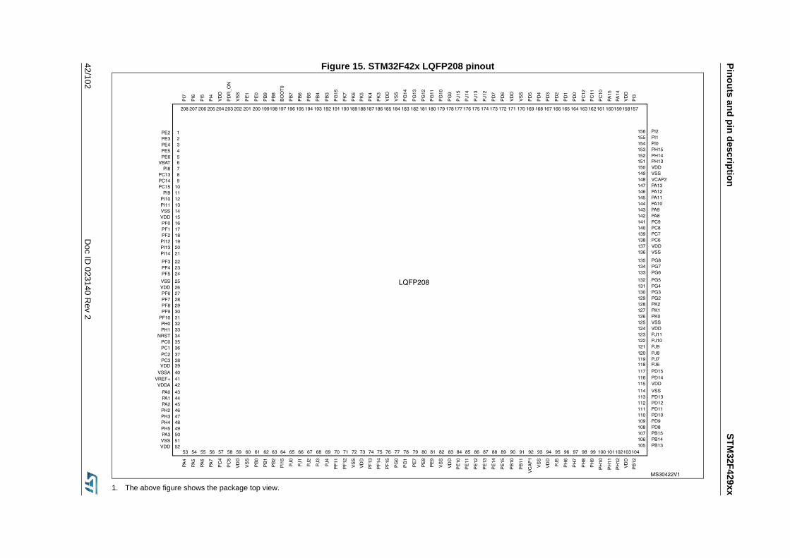
Figure 15. STM32F42x LQFP208 pinout
1. The above figure shows the package top view.

Doc ID 023140 Rev 2 43/102
STM32F429xx Pinouts and pin description
Figure 16. STM32F42x UFBGA176 ballout
1. The above figure shows the package top view.
Pinouts and pin descriptionSTM
32F429xx
44/102D
oc ID 023140 R
ev 2
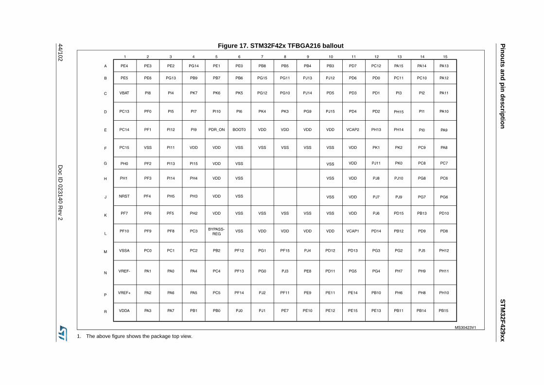
Figure 17. STM32F42x TFBGA216 ballout
1. The above figure shows the package top view.
Doc ID 023140 Rev 2 45/102
STM32F429xx Pinouts and pin description
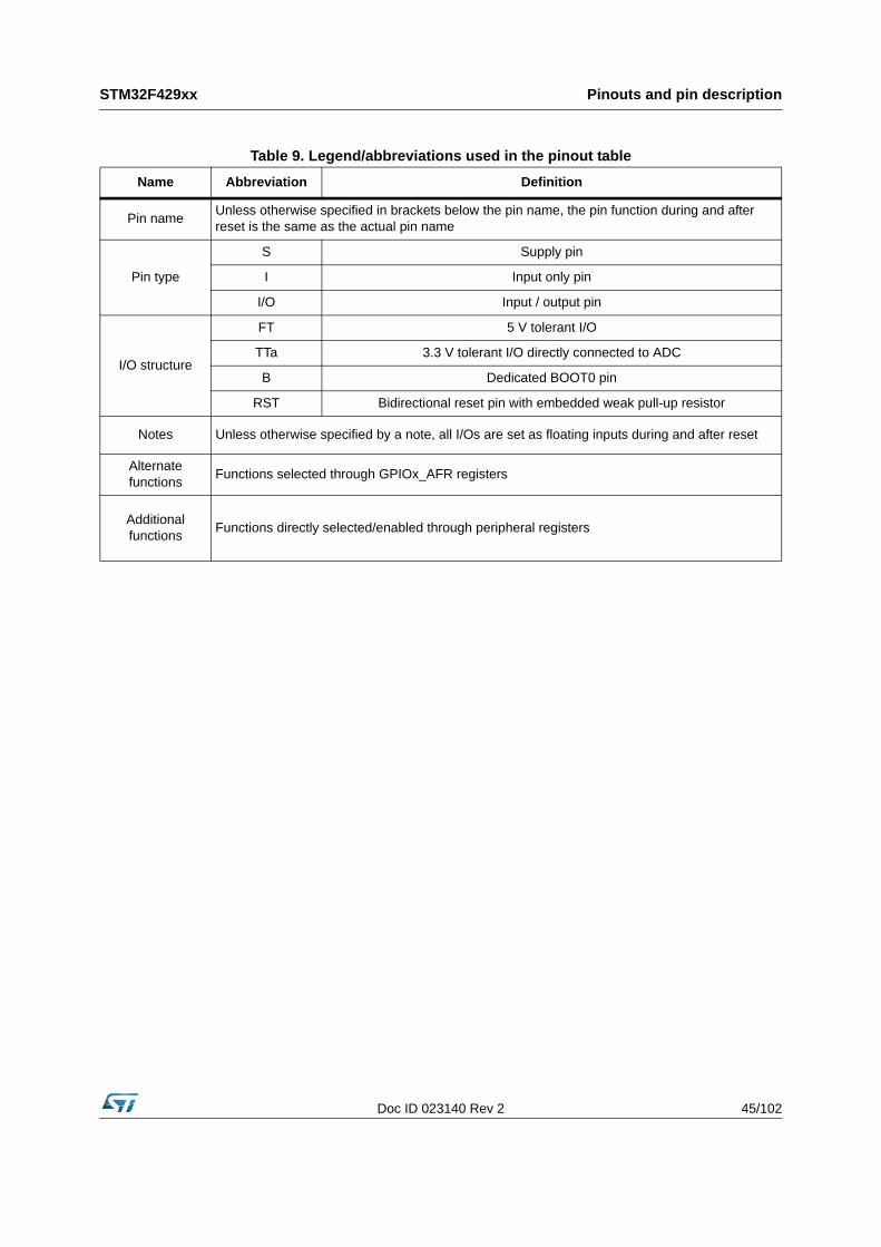
Table 9. Legend/abbreviations used in the pinout table
Name Abbreviation Definition
Pin name Unless otherwise specified in brackets below the pin name, the pin function during and after reset is the same as the actual pin name
Pin type
S Supply pin
I Input only pin
I/O Input / output pin
I/O structure
FT 5 V tolerant I/O
TTa 3.3 V tolerant I/O directly connected to ADC
B Dedicated BOOT0 pin
RST Bidirectional reset pin with embedded weak pull-up resistor
Notes Unless otherwise specified by a note, all I/Os are set as floating inputs during and after reset
Alternate functions Functions selected through GPIOx_AFR registers
Additional functions Functions directly selected/enabled through peripheral registers
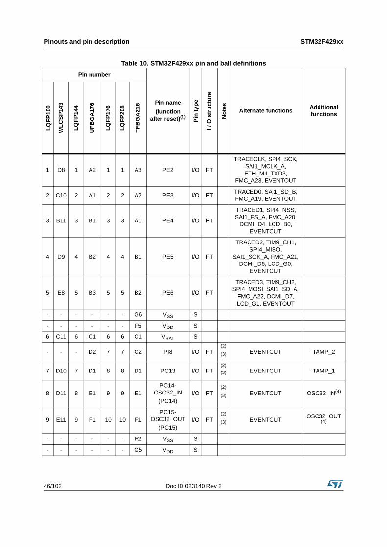
Pinouts and pin description STM32F429xx
46/102 Doc ID 023140 Rev 2
Table 10. STM32F429xx pin and ball definitions
Pin number
Pin name(function
after reset)(1) Pin
type
I / O
str
uctu
re
Not
es Alternate functions Additional functions
LQFP
100
WLC
SP14
3
LQFP
144
UFB
GA
176
LQFP
176
LQFP
208
TFB
GA
216
1 D8 1 A2 1 1 A3 PE2 I/O FT
TRACECLK, SPI4_SCK, SAI1_MCLK_A, ETH_MII_TXD3,
FMC_A23, EVENTOUT
2 C10 2 A1 2 2 A2 PE3 I/O FT TRACED0, SAI1_SD_B, FMC_A19, EVENTOUT
3 B11 3 B1 3 3 A1 PE4 I/O FT
TRACED1, SPI4_NSS, SAI1_FS_A, FMC_A20,
DCMI_D4, LCD_B0, EVENTOUT
4 D9 4 B2 4 4 B1 PE5 I/O FT
TRACED2, TIM9_CH1, SPI4_MISO,
SAI1_SCK_A, FMC_A21, DCMI_D6, LCD_G0,
EVENTOUT
5 E8 5 B3 5 5 B2 PE6 I/O FT
TRACED3, TIM9_CH2, SPI4_MOSI, SAI1_SD_A,
FMC_A22, DCMI_D7, LCD_G1, EVENTOUT
- - - - - - G6 VSS S
- - - - - - F5 VDD S
6 C11 6 C1 6 6 C1 VBAT S
- - - D2 7 7 C2 PI8 I/O FT(2)
(3) EVENTOUT TAMP_2
7 D10 7 D1 8 8 D1 PC13 I/O FT(2)(3) EVENTOUT TAMP_1
8 D11 8 E1 9 9 E1PC14-
OSC32_IN(PC14)
I/O FT(2)
(3) EVENTOUT OSC32_IN(4)
9 E11 9 F1 10 10 F1PC15-
OSC32_OUT(PC15)
I/O FT(2)
(3) EVENTOUT OSC32_OUT(4)
- - - - - - F2 VSS S
- - - - - - G5 VDD S
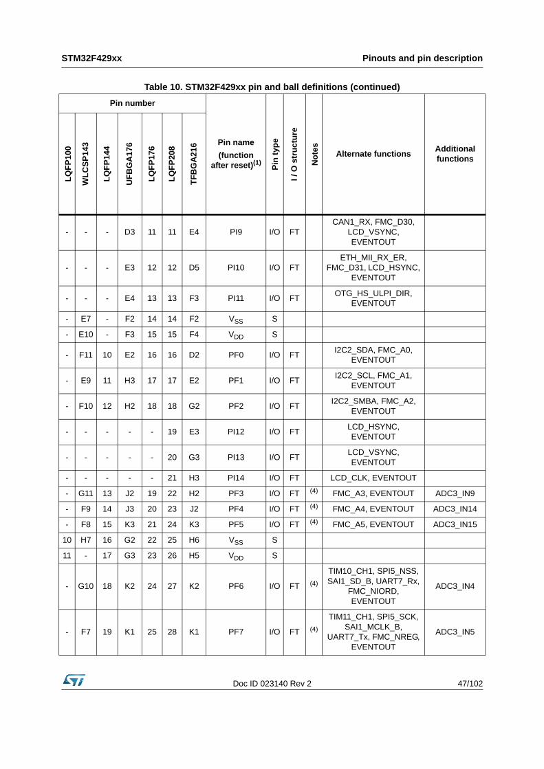
Doc ID 023140 Rev 2 47/102
STM32F429xx Pinouts and pin description
- - - D3 11 11 E4 PI9 I/O FTCAN1_RX, FMC_D30,
LCD_VSYNC, EVENTOUT
- - - E3 12 12 D5 PI10 I/O FTETH_MII_RX_ER,
FMC_D31, LCD_HSYNC, EVENTOUT
- - - E4 13 13 F3 PI11 I/O FT OTG_HS_ULPI_DIR, EVENTOUT
- E7 - F2 14 14 F2 VSS S
- E10 - F3 15 15 F4 VDD S
- F11 10 E2 16 16 D2 PF0 I/O FT I2C2_SDA, FMC_A0, EVENTOUT
- E9 11 H3 17 17 E2 PF1 I/O FT I2C2_SCL, FMC_A1, EVENTOUT
- F10 12 H2 18 18 G2 PF2 I/O FT I2C2_SMBA, FMC_A2, EVENTOUT
- - - - - 19 E3 PI12 I/O FT LCD_HSYNC, EVENTOUT
- - - - - 20 G3 PI13 I/O FT LCD_VSYNC, EVENTOUT
- - - - - 21 H3 PI14 I/O FT LCD_CLK, EVENTOUT
- G11 13 J2 19 22 H2 PF3 I/O FT (4) FMC_A3, EVENTOUT ADC3_IN9
- F9 14 J3 20 23 J2 PF4 I/O FT (4) FMC_A4, EVENTOUT ADC3_IN14
- F8 15 K3 21 24 K3 PF5 I/O FT (4) FMC_A5, EVENTOUT ADC3_IN15
10 H7 16 G2 22 25 H6 VSS S
11 - 17 G3 23 26 H5 VDD S
- G10 18 K2 24 27 K2 PF6 I/O FT (4)
TIM10_CH1, SPI5_NSS, SAI1_SD_B, UART7_Rx,
FMC_NIORD, EVENTOUT
ADC3_IN4
- F7 19 K1 25 28 K1 PF7 I/O FT (4)
TIM11_CH1, SPI5_SCK, SAI1_MCLK_B,
UART7_Tx, FMC_NREG, EVENTOUT
ADC3_IN5
Table 10. STM32F429xx pin and ball definitions (continued)
Pin number
Pin name(function
after reset)(1) Pin
type
I / O
str
uctu
re
Not
es Alternate functions Additional functions
LQFP
100
WLC
SP14
3
LQFP
144
UFB
GA
176
LQFP
176
LQFP
208
TFB
GA
216
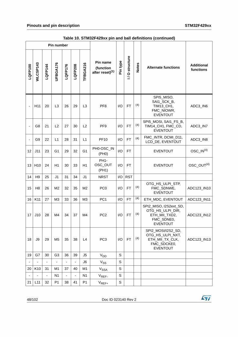
Pinouts and pin description STM32F429xx
48/102 Doc ID 023140 Rev 2
- H11 20 L3 26 29 L3 PF8 I/O FT (4)
SPI5_MISO, SAI1_SCK_B, TIM13_CH1,
FMC_NIOWR, EVENTOUT
ADC3_IN6
- G8 21 L2 27 30 L2 PF9 I/O FT (4)SPI5_MOSI, SAI1_FS_B, TIM14_CH1, FMC_CD,
EVENTOUTADC3_IN7
- G9 22 L1 28 31 L1 PF10 I/O FT (4) FMC_INTR, DCMI_D11, LCD_DE, EVENTOUT ADC3_IN8
12 J11 23 G1 29 32 G1PH0-OSC_IN
(PH0)I/O FT EVENTOUT OSC_IN(4)
13 H10 24 H1 30 33 H1PH1-
OSC_OUT(PH1)
I/O FT EVENTOUT OSC_OUT(4)
14 H9 25 J1 31 34 J1 NRST I/O RST
15 H8 26 M2 32 35 M2 PC0 I/O FT (4)OTG_HS_ULPI_STP,
FMC_SDNWE, EVENTOUT
ADC123_IN10
16 K11 27 M3 33 36 M3 PC1 I/O FT (4) ETH_MDC, EVENTOUT ADC123_IN11
17 J10 28 M4 34 37 M4 PC2 I/O FT (4)
SPI2_MISO, I2S2ext_SD, OTG_HS_ULPI_DIR,
ETH_MII_TXD2, FMC_SDNE0, EVENTOUT
ADC123_IN12
18 J9 29 M5 35 38 L4 PC3 I/O FT (4)
SPI2_MOSI/I2S2_SD, OTG_HS_ULPI_NXT, ETH_MII_TX_CLK,
FMC_SDCKE0, EVENTOUT
ADC123_IN13
19 G7 30 G3 36 39 J5 VDD S
- - - - - - J6 VSS S
20 K10 31 M1 37 40 M1 VSSA S
- - - N1 - - N1 VREF– S
21 L11 32 P1 38 41 P1 VREF+ S
Table 10. STM32F429xx pin and ball definitions (continued)
Pin number
Pin name(function
after reset)(1) Pin
type
I / O
str
uctu
re
Not
es Alternate functions Additional functions
LQFP
100
WLC
SP14
3
LQFP
144
UFB
GA
176
LQFP
176
LQFP
208
TFB
GA
216

Doc ID 023140 Rev 2 49/102
STM32F429xx Pinouts and pin description
22 L10 33 R1 39 42 R1 VDDA S
23 K9 34 N3 40 43 N3PA0-WKUP
(PA0)I/O FT (5)
TIM2_CH1/TIM2_ETR, TIM5_CH1, TIM8_ETR,
USART2_CTS, UART4_TX,
ETH_MII_CRS, EVENTOUT
ADC123_IN0/WKUP(4)
24 K8 35 N2 41 44 N2 PA1 I/O FT (4)
TIM2_CH2, TIM5_CH2, USART2_RTS,
UART4_RX, ETH_MII_RX_CLK/ETH_
RMII_REF_CLK, EVENTOUT
ADC123_IN1
25 L9 36 P2 42 45 P2 PA2 I/O FT (4)TIM2_CH3, TIM5_CH3,
TIM9_CH1, USART2_TX, ETH_MDIO, EVENTOUT
ADC123_IN2
- - - F4 43 46 K4 PH2 I/O FTETH_MII_CRS,
FMC_SDCKE0, LCD_R0, EVENTOUT
- - - G4 44 47 J4 PH3 I/O FTETH_MII_COL,
FMC_SDNE0, LCD_R1, EVENTOUT
- - - H4 45 48 H4 PH4 I/O FTI2C2_SCL,
OTG_HS_ULPI_NXT, EVENTOUT
- - - J4 46 49 J3 PH5 I/O FTI2C2_SDA, SPI5_NSS,
FMC_SDNWE, EVENTOUT
26 M11 37 R2 47 50 R2 PA3 I/O FT (4)
TIM2_CH4, TIM5_CH4, TIM9_CH2, USART2_RX,
OTG_HS_ULPI_D0, ETH_MII_COL, LCD_B5,
EVENTOUT
ADC123_IN3
27 - 38 - 51 K6 VSS S
- N11 - L4 48 - L5 BYPASS_REG I FT
28 J8 39 K4 49 52 K5 VDD S
Table 10. STM32F429xx pin and ball definitions (continued)
Pin number
Pin name(function
after reset)(1) Pin
type
I / O
str
uctu
re
Not
es Alternate functions Additional functions
LQFP
100
WLC
SP14
3
LQFP
144
UFB
GA
176
LQFP
176
LQFP
208
TFB
GA
216
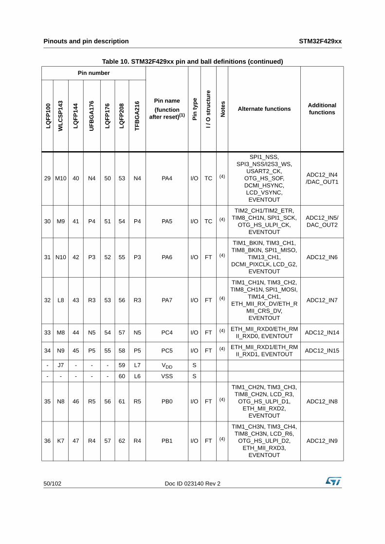
Pinouts and pin description STM32F429xx
50/102 Doc ID 023140 Rev 2
29 M10 40 N4 50 53 N4 PA4 I/O TC (4)
SPI1_NSS, SPI3_NSS/I2S3_WS,
USART2_CK, OTG_HS_SOF, DCMI_HSYNC, LCD_VSYNC, EVENTOUT
ADC12_IN4 /DAC_OUT1
30 M9 41 P4 51 54 P4 PA5 I/O TC (4)
TIM2_CH1/TIM2_ETR, TIM8_CH1N, SPI1_SCK,
OTG_HS_ULPI_CK, EVENTOUT
ADC12_IN5/DAC_OUT2
31 N10 42 P3 52 55 P3 PA6 I/O FT (4)
TIM1_BKIN, TIM3_CH1, TIM8_BKIN, SPI1_MISO,
TIM13_CH1, DCMI_PIXCLK, LCD_G2,
EVENTOUT
ADC12_IN6
32 L8 43 R3 53 56 R3 PA7 I/O FT (4)
TIM1_CH1N, TIM3_CH2, TIM8_CH1N, SPI1_MOSI,
TIM14_CH1, ETH_MII_RX_DV/ETH_R
MII_CRS_DV, EVENTOUT
ADC12_IN7
33 M8 44 N5 54 57 N5 PC4 I/O FT (4) ETH_MII_RXD0/ETH_RMII_RXD0, EVENTOUT ADC12_IN14
34 N9 45 P5 55 58 P5 PC5 I/O FT (4) ETH_MII_RXD1/ETH_RMII_RXD1, EVENTOUT ADC12_IN15
- J7 - - - 59 L7 VDD S
- - - - - 60 L6 VSS S
35 N8 46 R5 56 61 R5 PB0 I/O FT (4)
TIM1_CH2N, TIM3_CH3, TIM8_CH2N, LCD_R3,
OTG_HS_ULPI_D1, ETH_MII_RXD2,
EVENTOUT
ADC12_IN8
36 K7 47 R4 57 62 R4 PB1 I/O FT (4)
TIM1_CH3N, TIM3_CH4, TIM8_CH3N, LCD_R6,
OTG_HS_ULPI_D2, ETH_MII_RXD3,
EVENTOUT
ADC12_IN9
Table 10. STM32F429xx pin and ball definitions (continued)
Pin number
Pin name(function
after reset)(1) Pin
type
I / O
str
uctu
re
Not
es Alternate functions Additional functions
LQFP
100
WLC
SP14
3
LQFP
144
UFB
GA
176
LQFP
176
LQFP
208
TFB
GA
216
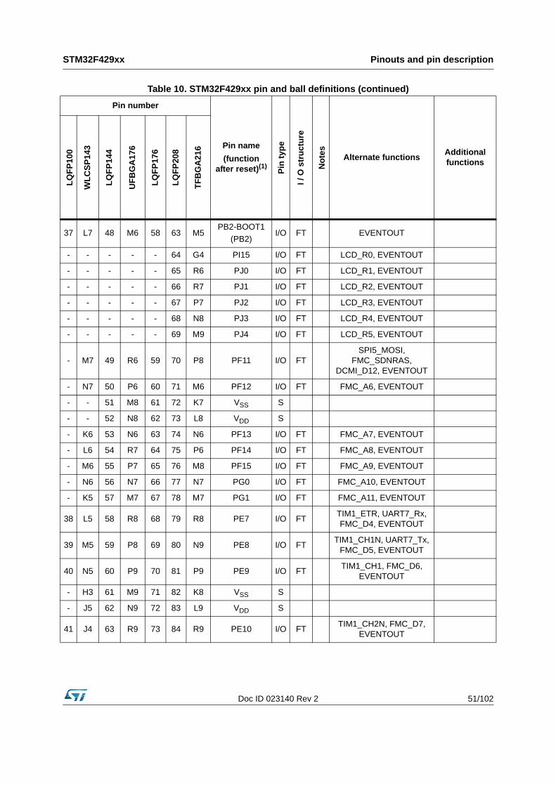
Doc ID 023140 Rev 2 51/102
STM32F429xx Pinouts and pin description
37 L7 48 M6 58 63 M5PB2-BOOT1
(PB2)I/O FT EVENTOUT
- - - - - 64 G4 PI15 I/O FT LCD_R0, EVENTOUT
- - - - - 65 R6 PJ0 I/O FT LCD_R1, EVENTOUT
- - - - - 66 R7 PJ1 I/O FT LCD_R2, EVENTOUT
- - - - - 67 P7 PJ2 I/O FT LCD_R3, EVENTOUT
- - - - - 68 N8 PJ3 I/O FT LCD_R4, EVENTOUT
- - - - - 69 M9 PJ4 I/O FT LCD_R5, EVENTOUT
- M7 49 R6 59 70 P8 PF11 I/O FTSPI5_MOSI,
FMC_SDNRAS, DCMI_D12, EVENTOUT
- N7 50 P6 60 71 M6 PF12 I/O FT FMC_A6, EVENTOUT
- - 51 M8 61 72 K7 VSS S
- - 52 N8 62 73 L8 VDD S
- K6 53 N6 63 74 N6 PF13 I/O FT FMC_A7, EVENTOUT
- L6 54 R7 64 75 P6 PF14 I/O FT FMC_A8, EVENTOUT
- M6 55 P7 65 76 M8 PF15 I/O FT FMC_A9, EVENTOUT
- N6 56 N7 66 77 N7 PG0 I/O FT FMC_A10, EVENTOUT
- K5 57 M7 67 78 M7 PG1 I/O FT FMC_A11, EVENTOUT
38 L5 58 R8 68 79 R8 PE7 I/O FT TIM1_ETR, UART7_Rx, FMC_D4, EVENTOUT
39 M5 59 P8 69 80 N9 PE8 I/O FT TIM1_CH1N, UART7_Tx, FMC_D5, EVENTOUT
40 N5 60 P9 70 81 P9 PE9 I/O FT TIM1_CH1, FMC_D6, EVENTOUT
- H3 61 M9 71 82 K8 VSS S
- J5 62 N9 72 83 L9 VDD S
41 J4 63 R9 73 84 R9 PE10 I/O FT TIM1_CH2N, FMC_D7, EVENTOUT
Table 10. STM32F429xx pin and ball definitions (continued)
Pin number
Pin name(function
after reset)(1) Pin
type
I / O
str
uctu
re
Not
es Alternate functions Additional functions
LQFP
100
WLC
SP14
3
LQFP
144
UFB
GA
176
LQFP
176
LQFP
208
TFB
GA
216
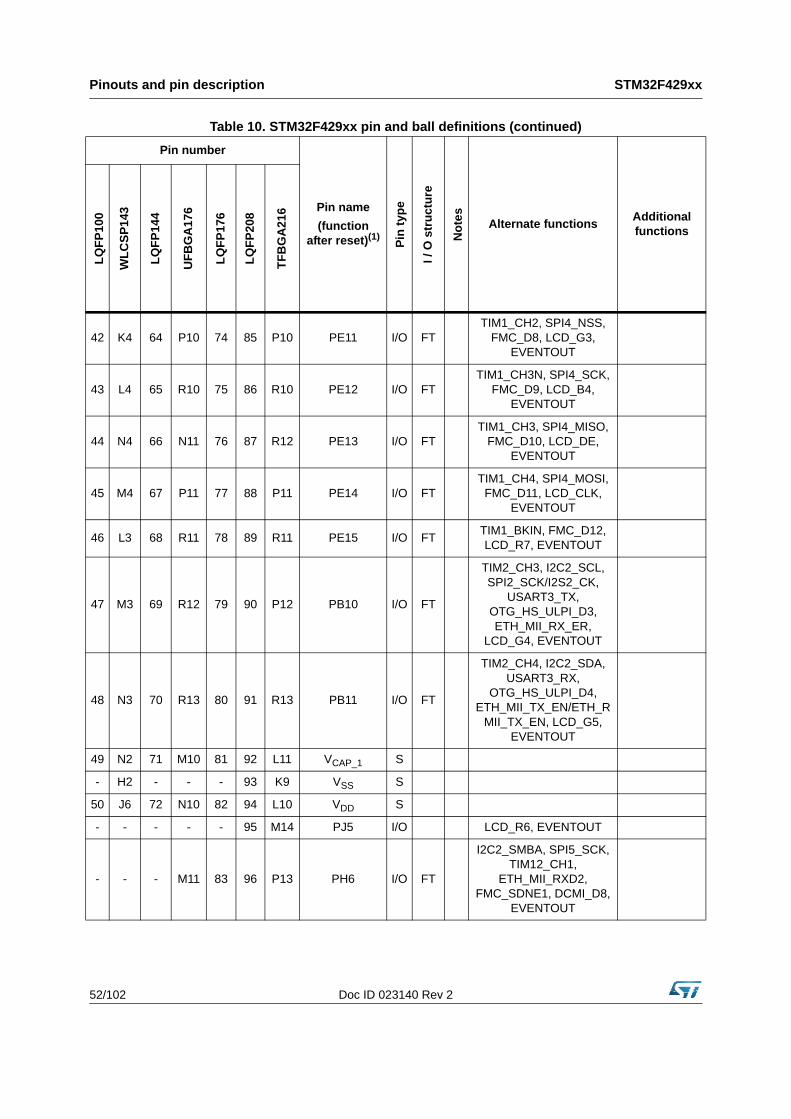
Pinouts and pin description STM32F429xx
52/102 Doc ID 023140 Rev 2
42 K4 64 P10 74 85 P10 PE11 I/O FTTIM1_CH2, SPI4_NSS,
FMC_D8, LCD_G3, EVENTOUT
43 L4 65 R10 75 86 R10 PE12 I/O FTTIM1_CH3N, SPI4_SCK,
FMC_D9, LCD_B4, EVENTOUT
44 N4 66 N11 76 87 R12 PE13 I/O FTTIM1_CH3, SPI4_MISO,
FMC_D10, LCD_DE, EVENTOUT
45 M4 67 P11 77 88 P11 PE14 I/O FTTIM1_CH4, SPI4_MOSI,
FMC_D11, LCD_CLK, EVENTOUT
46 L3 68 R11 78 89 R11 PE15 I/O FT TIM1_BKIN, FMC_D12, LCD_R7, EVENTOUT
47 M3 69 R12 79 90 P12 PB10 I/O FT
TIM2_CH3, I2C2_SCL, SPI2_SCK/I2S2_CK,
USART3_TX, OTG_HS_ULPI_D3, ETH_MII_RX_ER,
LCD_G4, EVENTOUT
48 N3 70 R13 80 91 R13 PB11 I/O FT
TIM2_CH4, I2C2_SDA, USART3_RX,
OTG_HS_ULPI_D4, ETH_MII_TX_EN/ETH_R
MII_TX_EN, LCD_G5, EVENTOUT
49 N2 71 M10 81 92 L11 VCAP_1 S
- H2 - - - 93 K9 VSS S
50 J6 72 N10 82 94 L10 VDD S
- - - - - 95 M14 PJ5 I/O LCD_R6, EVENTOUT
- - - M11 83 96 P13 PH6 I/O FT
I2C2_SMBA, SPI5_SCK, TIM12_CH1,
ETH_MII_RXD2, FMC_SDNE1, DCMI_D8,
EVENTOUT
Table 10. STM32F429xx pin and ball definitions (continued)
Pin number
Pin name(function
after reset)(1) Pin
type
I / O
str
uctu
re
Not
es Alternate functions Additional functions
LQFP
100
WLC
SP14
3
LQFP
144
UFB
GA
176
LQFP
176
LQFP
208
TFB
GA
216
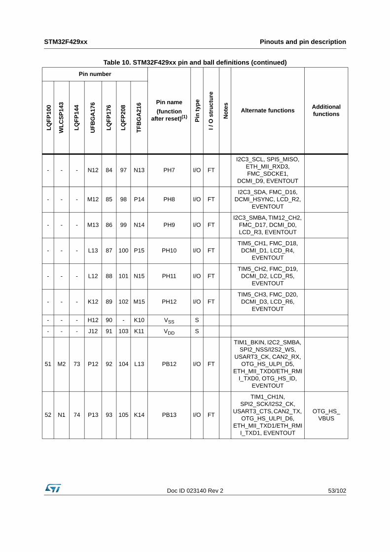
Doc ID 023140 Rev 2 53/102
STM32F429xx Pinouts and pin description
- - - N12 84 97 N13 PH7 I/O FT
I2C3_SCL, SPI5_MISO, ETH_MII_RXD3, FMC_SDCKE1,
DCMI_D9, EVENTOUT
- - - M12 85 98 P14 PH8 I/O FTI2C3_SDA, FMC_D16,
DCMI_HSYNC, LCD_R2, EVENTOUT
- - - M13 86 99 N14 PH9 I/O FTI2C3_SMBA, TIM12_CH2,
FMC_D17, DCMI_D0, LCD_R3, EVENTOUT
- - - L13 87 100 P15 PH10 I/O FTTIM5_CH1, FMC_D18,
DCMI_D1, LCD_R4, EVENTOUT
- - - L12 88 101 N15 PH11 I/O FTTIM5_CH2, FMC_D19,
DCMI_D2, LCD_R5, EVENTOUT
- - - K12 89 102 M15 PH12 I/O FTTIM5_CH3, FMC_D20,
DCMI_D3, LCD_R6, EVENTOUT
- - - H12 90 - K10 VSS S
- - - J12 91 103 K11 VDD S
51 M2 73 P12 92 104 L13 PB12 I/O FT
TIM1_BKIN, I2C2_SMBA, SPI2_NSS/I2S2_WS,
USART3_CK, CAN2_RX, OTG_HS_ULPI_D5,
ETH_MII_TXD0/ETH_RMII_TXD0, OTG_HS_ID,
EVENTOUT
52 N1 74 P13 93 105 K14 PB13 I/O FT
TIM1_CH1N, SPI2_SCK/I2S2_CK,
USART3_CTS, CAN2_TX, OTG_HS_ULPI_D6,
ETH_MII_TXD1/ETH_RMII_TXD1, EVENTOUT
OTG_HS_VBUS
Table 10. STM32F429xx pin and ball definitions (continued)
Pin number
Pin name(function
after reset)(1) Pin
type
I / O
str
uctu
re
Not
es Alternate functions Additional functions
LQFP
100
WLC
SP14
3
LQFP
144
UFB
GA
176
LQFP
176
LQFP
208
TFB
GA
216
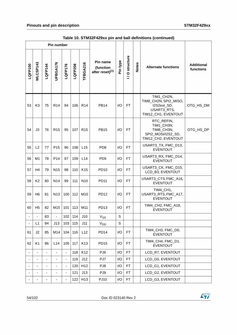
Pinouts and pin description STM32F429xx
54/102 Doc ID 023140 Rev 2
53 K3 75 R14 94 106 R14 PB14 I/O FT
TIM1_CH2N, TIM8_CH2N, SPI2_MISO,
I2S2ext_SD, USART3_RTS,
TIM12_CH1, EVENTOUT
OTG_HS_DM
54 J3 76 R15 95 107 R15 PB15 I/O FT
RTC_REFIN, TIM1_CH3N, TIM8_CH3N,
SPI2_MOSI/I2S2_SD, TIM12_CH2, EVENTOUT
OTG_HS_DP
55 L2 77 P15 96 108 L15 PD8 I/O FT USART3_TX, FMC_D13, EVENTOUT
56 M1 78 P14 97 109 L14 PD9 I/O FT USART3_RX, FMC_D14, EVENTOUT
57 H4 79 N15 98 110 K15 PD10 I/O FT USART3_CK, FMC_D15, LCD_B3, EVENTOUT
58 K2 80 N14 99 111 N10 PD11 I/O FT USART3_CTS, FMC_A16, EVENTOUT
59 H6 81 N13 100 112 M10 PD12 I/O FTTIM4_CH1,
USART3_RTS, FMC_A17, EVENTOUT
60 H5 82 M15 101 113 M11 PD13 I/O FT TIM4_CH2, FMC_A18, EVENTOUT
- - 83 - 102 114 J10 VSS S
- L1 84 J13 103 115 J11 VDD S
61 J2 85 M14 104 116 L12 PD14 I/O FT TIM4_CH3, FMC_D0, EVENTOUT
62 K1 86 L14 105 117 K13 PD15 I/O FT TIM4_CH4, FMC_D1, EVENTOUT
- - - - - 118 K12 PJ6 I/O FT LCD_R7, EVENTOUT
- - - - - 119 J12 PJ7 I/O FT LCD_G0, EVENTOUT
- - - - - 120 H12 PJ8 I/O FT LCD_G1, EVENTOUT
- - - - - 121 J13 PJ9 I/O FT LCD_G2, EVENTOUT
- - - - - 122 H13 PJ10 I/O FT LCD_G3, EVENTOUT
Table 10. STM32F429xx pin and ball definitions (continued)
Pin number
Pin name(function
after reset)(1) Pin
type
I / O
str
uctu
re
Not
es Alternate functions Additional functions
LQFP
100
WLC
SP14
3
LQFP
144
UFB
GA
176
LQFP
176
LQFP
208
TFB
GA
216
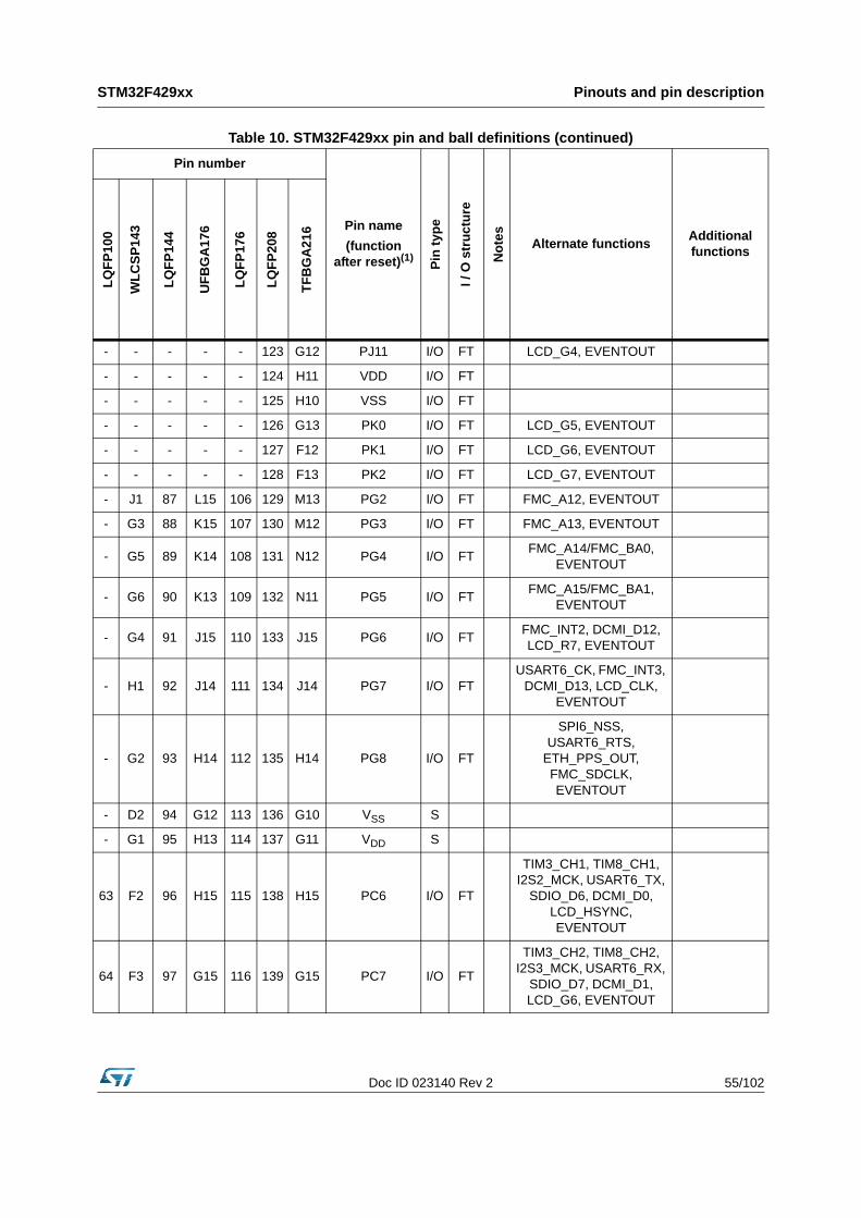
Doc ID 023140 Rev 2 55/102
STM32F429xx Pinouts and pin description
- - - - - 123 G12 PJ11 I/O FT LCD_G4, EVENTOUT
- - - - - 124 H11 VDD I/O FT
- - - - - 125 H10 VSS I/O FT
- - - - - 126 G13 PK0 I/O FT LCD_G5, EVENTOUT
- - - - - 127 F12 PK1 I/O FT LCD_G6, EVENTOUT
- - - - - 128 F13 PK2 I/O FT LCD_G7, EVENTOUT
- J1 87 L15 106 129 M13 PG2 I/O FT FMC_A12, EVENTOUT
- G3 88 K15 107 130 M12 PG3 I/O FT FMC_A13, EVENTOUT
- G5 89 K14 108 131 N12 PG4 I/O FT FMC_A14/FMC_BA0, EVENTOUT
- G6 90 K13 109 132 N11 PG5 I/O FT FMC_A15/FMC_BA1, EVENTOUT
- G4 91 J15 110 133 J15 PG6 I/O FT FMC_INT2, DCMI_D12, LCD_R7, EVENTOUT
- H1 92 J14 111 134 J14 PG7 I/O FTUSART6_CK, FMC_INT3,
DCMI_D13, LCD_CLK, EVENTOUT
- G2 93 H14 112 135 H14 PG8 I/O FT
SPI6_NSS, USART6_RTS,
ETH_PPS_OUT, FMC_SDCLK, EVENTOUT
- D2 94 G12 113 136 G10 VSS S
- G1 95 H13 114 137 G11 VDD S
63 F2 96 H15 115 138 H15 PC6 I/O FT
TIM3_CH1, TIM8_CH1, I2S2_MCK, USART6_TX,
SDIO_D6, DCMI_D0, LCD_HSYNC, EVENTOUT
64 F3 97 G15 116 139 G15 PC7 I/O FT
TIM3_CH2, TIM8_CH2, I2S3_MCK, USART6_RX,
SDIO_D7, DCMI_D1, LCD_G6, EVENTOUT
Table 10. STM32F429xx pin and ball definitions (continued)
Pin number
Pin name(function
after reset)(1) Pin
type
I / O
str
uctu
re
Not
es Alternate functions Additional functions
LQFP
100
WLC
SP14
3
LQFP
144
UFB
GA
176
LQFP
176
LQFP
208
TFB
GA
216
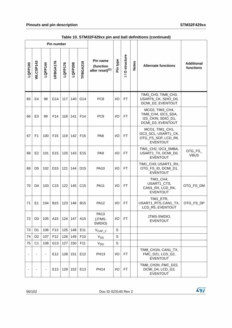
Pinouts and pin description STM32F429xx
56/102 Doc ID 023140 Rev 2
65 E4 98 G14 117 140 G14 PC8 I/O FTTIM3_CH3, TIM8_CH3, USART6_CK, SDIO_D0, DCMI_D2, EVENTOUT
66 E3 99 F14 118 141 F14 PC9 I/O FT
MCO2, TIM3_CH4, TIM8_CH4, I2C3_SDA, I2S_CKIN, SDIO_D1,
DCMI_D3, EVENTOUT
67 F1 100 F15 119 142 F15 PA8 I/O FT
MCO1, TIM1_CH1, I2C3_SCL, USART1_CK, OTG_FS_SOF, LCD_R6,
EVENTOUT
68 E2 101 E15 120 143 E15 PA9 I/O FTTIM1_CH2, I2C3_SMBA, USART1_TX, DCMI_D0,
EVENTOUT
OTG_FS_VBUS
69 D5 102 D15 121 144 D15 PA10 I/O FTTIM1_CH3, USART1_RX, OTG_FS_ID, DCMI_D1,
EVENTOUT
70 D4 103 C15 122 145 C15 PA11 I/O FT
TIM1_CH4, USART1_CTS,
CAN1_RX, LCD_R4, EVENTOUT
OTG_FS_DM
71 E1 104 B15 123 146 B15 PA12 I/O FTTIM1_ETR,
USART1_RTS, CAN1_TX, LCD_R5, EVENTOUT
OTG_FS_DP
72 D3 105 A15 124 147 A15PA13
(JTMS-SWDIO)
I/O FT JTMS-SWDIO, EVENTOUT
73 D1 106 F13 125 148 E11 VCAP_2 S
74 D2 107 F12 126 149 F10 VSS S
75 C1 108 G13 127 150 F11 VDD S
- - - E12 128 151 E12 PH13 I/O FTTIM8_CH1N, CAN1_TX,
FMC_D21, LCD_G2, EVENTOUT
- - - E13 129 152 E13 PH14 I/O FTTIM8_CH2N, FMC_D22,
DCMI_D4, LCD_G3, EVENTOUT
Table 10. STM32F429xx pin and ball definitions (continued)
Pin number
Pin name(function
after reset)(1) Pin
type
I / O
str
uctu
re
Not
es Alternate functions Additional functions
LQFP
100
WLC
SP14
3
LQFP
144
UFB
GA
176
LQFP
176
LQFP
208
TFB
GA
216
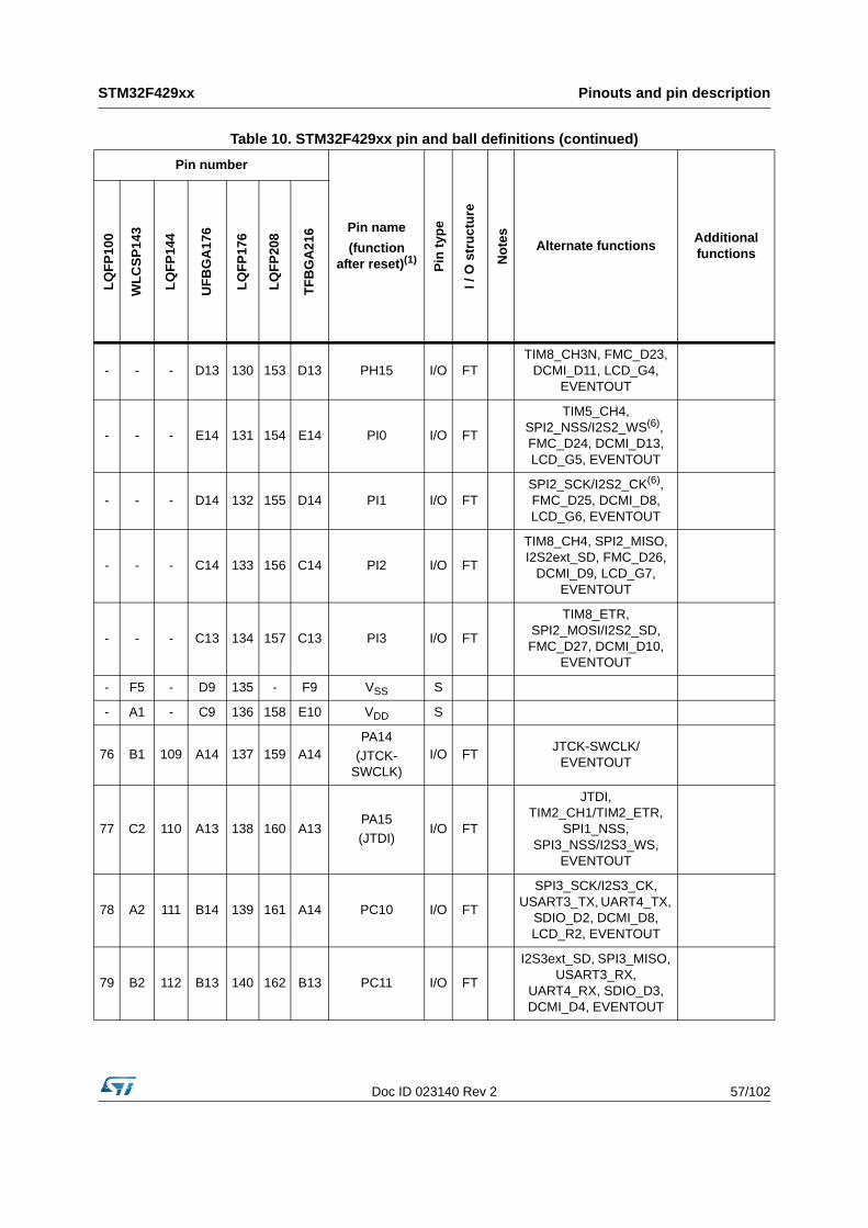
Doc ID 023140 Rev 2 57/102
STM32F429xx Pinouts and pin description
- - - D13 130 153 D13 PH15 I/O FTTIM8_CH3N, FMC_D23,
DCMI_D11, LCD_G4, EVENTOUT
- - - E14 131 154 E14 PI0 I/O FT
TIM5_CH4, SPI2_NSS/I2S2_WS(6), FMC_D24, DCMI_D13, LCD_G5, EVENTOUT
- - - D14 132 155 D14 PI1 I/O FTSPI2_SCK/I2S2_CK(6), FMC_D25, DCMI_D8, LCD_G6, EVENTOUT
- - - C14 133 156 C14 PI2 I/O FT
TIM8_CH4, SPI2_MISO, I2S2ext_SD, FMC_D26,
DCMI_D9, LCD_G7, EVENTOUT
- - - C13 134 157 C13 PI3 I/O FT
TIM8_ETR, SPI2_MOSI/I2S2_SD, FMC_D27, DCMI_D10,
EVENTOUT
- F5 - D9 135 - F9 VSS S
- A1 - C9 136 158 E10 VDD S
76 B1 109 A14 137 159 A14PA14
(JTCK-SWCLK)
I/O FT JTCK-SWCLK/ EVENTOUT
77 C2 110 A13 138 160 A13PA15(JTDI)
I/O FT
JTDI, TIM2_CH1/TIM2_ETR,
SPI1_NSS, SPI3_NSS/I2S3_WS,
EVENTOUT
78 A2 111 B14 139 161 A14 PC10 I/O FT
SPI3_SCK/I2S3_CK, USART3_TX, UART4_TX,
SDIO_D2, DCMI_D8, LCD_R2, EVENTOUT
79 B2 112 B13 140 162 B13 PC11 I/O FT
I2S3ext_SD, SPI3_MISO, USART3_RX,
UART4_RX, SDIO_D3, DCMI_D4, EVENTOUT
Table 10. STM32F429xx pin and ball definitions (continued)
Pin number
Pin name(function
after reset)(1) Pin
type
I / O
str
uctu
re
Not
es Alternate functions Additional functions
LQFP
100
WLC
SP14
3
LQFP
144
UFB
GA
176
LQFP
176
LQFP
208
TFB
GA
216
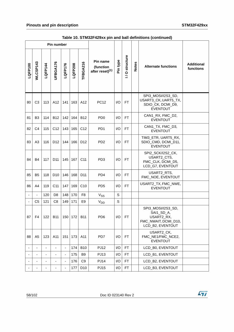
Pinouts and pin description STM32F429xx
58/102 Doc ID 023140 Rev 2
80 C3 113 A12 141 163 A12 PC12 I/O FT
SPI3_MOSI/I2S3_SD, USART3_CK, UART5_TX,
SDIO_CK, DCMI_D9, EVENTOUT
81 B3 114 B12 142 164 B12 PD0 I/O FT CAN1_RX, FMC_D2, EVENTOUT
82 C4 115 C12 143 165 C12 PD1 I/O FT CAN1_TX, FMC_D3, EVENTOUT
83 A3 116 D12 144 166 D12 PD2 I/O FTTIM3_ETR, UART5_RX, SDIO_CMD, DCMI_D11,
EVENTOUT
84 B4 117 D11 145 167 C11 PD3 I/O FT
SPI2_SCK/I2S2_CK, USART2_CTS,
FMC_CLK, DCMI_D5, LCD_G7, EVENTOUT
85 B5 118 D10 146 168 D11 PD4 I/O FT USART2_RTS, FMC_NOE, EVENTOUT
86 A4 119 C11 147 169 C10 PD5 I/O FT USART2_TX, FMC_NWE, EVENTOUT
- - 120 D8 148 170 F8 VSS S
- C5 121 C8 149 171 E9 VDD S
87 F4 122 B11 150 172 B11 PD6 I/O FT
SPI3_MOSI/I2S3_SD, SAI1_SD_A, USART2_RX,
FMC_NWAIT, DCMI_D10, LCD_B2, EVENTOUT
88 A5 123 A11 151 173 A11 PD7 I/O FTUSART2_CK,
FMC_NE1/FMC_NCE2, EVENTOUT
- - - - - 174 B10 PJ12 I/O FT LCD_B0, EVENTOUT
- - - - - 175 B9 PJ13 I/O FT LCD_B1, EVENTOUT
- - - - - 176 C9 PJ14 I/O FT LCD_B2, EVENTOUT
- - - - - 177 D10 PJ15 I/O FT LCD_B3, EVENTOUT
Table 10. STM32F429xx pin and ball definitions (continued)
Pin number
Pin name(function
after reset)(1) Pin
type
I / O
str
uctu
re
Not
es Alternate functions Additional functions
LQFP
100
WLC
SP14
3
LQFP
144
UFB
GA
176
LQFP
176
LQFP
208
TFB
GA
216

Doc ID 023140 Rev 2 59/102
STM32F429xx Pinouts and pin description
- E5 124 C10 152 178 D9 PG9 I/O FTUSART6_RX,
FMC_NE2/FMC_NCE3, EVENTOUT
- C6 125 B10 153 179 C8 PG10 I/O FT
LCD_G3, FMC_NCE4_1/FMC_NE3,
DCMI_D2, LCD_B2, EVENTOUT
- B6 126 B9 154 180 B8 PG11 I/O FT
ETH_MII_TX_EN/ETH_RMII_TX_EN,
FMC_NCE4_2, DCMI_D3, LCD_B3, EVENTOUT
- A6 127 B8 155 181 C7 PG12 I/O FT
SPI6_MISO, USART6_RTS, LCD_B4,
FMC_NE4, LCD_B1, EVENTOUT
- D6 128 A8 156 182 B3 PG13 I/O FT
SPI6_SCK, USART6_CTS,
ETH_MII_TXD0/ETH_RMII_TXD0, FMC_A24,
EVENTOUT
- F6 129 A7 157 183 A4 PG14 I/O FT
SPI6_MOSI, USART6_TX,
ETH_MII_TXD1/ETH_RMII_TXD1, FMC_A25,
EVENTOUT
- - 130 D7 158 184 F7 VSS S
- E6 131 C7 159 185 E8 VDD S
- - - - - 186 D8 PK3 I/O FT LCD_B4, EVENTOUT
- - - - - 187 D7 PK4 I/O FT LCD_B5, EVENTOUT
- - - - - 188 C6 PK5 I/O FT LCD_B6, EVENTOUT
- - - - - 189 C5 PK6 I/O FT LCD_B7, EVENTOUT
- - - - - 190 C4 PK7 I/O FT LCD_DE, EVENTOUT
- A7 132 B7 160 191 B7 PG15 I/O FTUSART6_CTS, FMC_SDNCAS,
DCMI_D13, EVENTOUT
Table 10. STM32F429xx pin and ball definitions (continued)
Pin number
Pin name(function
after reset)(1) Pin
type
I / O
str
uctu
re
Not
es Alternate functions Additional functions
LQFP
100
WLC
SP14
3
LQFP
144
UFB
GA
176
LQFP
176
LQFP
208
TFB
GA
216

Pinouts and pin description STM32F429xx
60/102 Doc ID 023140 Rev 2
89 B7 133 A10 161 192 A10PB3
(JTDO/TRACESWO)
I/O FT
JTDO/TRACESWO, TIM2_CH2, SPI1_SCK,
SPI3_SCK/I2S3_CK, EVENTOUT
90 C7 134 A9 162 193 A9PB4
(NJTRST)I/O FT
NJTRST, TIM3_CH1, SPI1_MISO, SPI3_MISO, I2S3ext_SD, EVENTOUT
91 C8 135 A6 163 194 A8 PB5 I/O FT
TIM3_CH2, I2C1_SMBA, SPI1_MOSI,
SPI3_MOSI/I2S3_SD, CAN2_RX,
OTG_HS_ULPI_D7, ETH_PPS_OUT, FMC_SDCKE1,
DCMI_D10, EVENTOUT
92 A8 136 B6 164 195 B6 PB6 I/O FT
TIM4_CH1, I2C1_SCL, USART1_TX, CAN2_TX, FMC_SDNE1, DCMI_D5,
EVENTOUT
93 B8 137 B5 165 196 B5 PB7 I/O FT
TIM4_CH2, I2C1_SDA, USART1_RX, FMC_NL,
DCMI_VSYNC, EVENTOUT
94 C9 138 D6 166 197 E6 BOOT0 I B VPP
95 A9 139 A5 167 198 A7 PB8 I/O FT
TIM4_CH3, TIM10_CH1, I2C1_SCL, CAN1_RX,
ETH_MII_TXD3, SDIO_D4, DCMI_D6, LCD_B6, EVENTOUT
96 B9 140 B4 168 199 B4 PB9 I/O FT
TIM4_CH4, TIM11_CH1, I2C1_SDA,
SPI2_NSS/I2S2_WS, CAN1_TX, SDIO_D5, DCMI_D7, LCD_B7,
EVENTOUT
97 B10 141 A4 169 200 A6 PE0 I/O FTTIM4_ETR, UART8_Rx, FMC_NBL0, DCMI_D2,
EVENTOUT
Table 10. STM32F429xx pin and ball definitions (continued)
Pin number
Pin name(function
after reset)(1) Pin
type
I / O
str
uctu
re
Not
es Alternate functions Additional functions
LQFP
100
WLC
SP14
3
LQFP
144
UFB
GA
176
LQFP
176
LQFP
208
TFB
GA
216
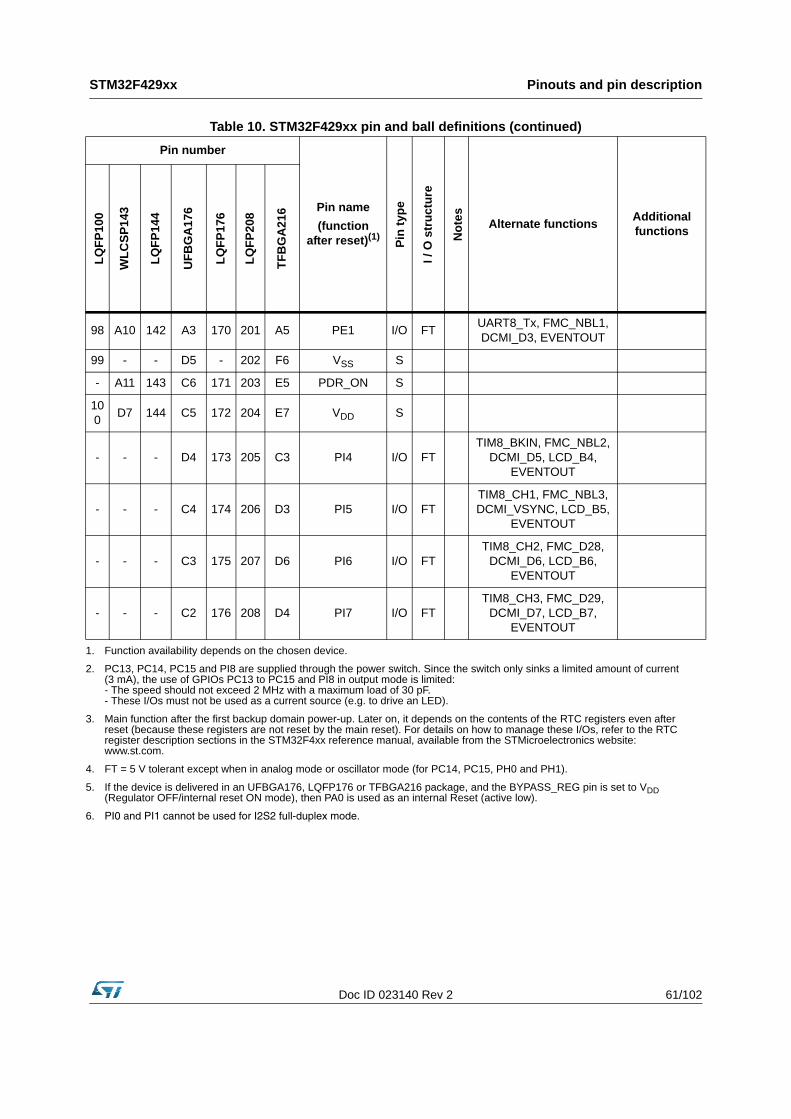
Doc ID 023140 Rev 2 61/102
STM32F429xx Pinouts and pin description
98 A10 142 A3 170 201 A5 PE1 I/O FT UART8_Tx, FMC_NBL1, DCMI_D3, EVENTOUT
99 - - D5 - 202 F6 VSS S
- A11 143 C6 171 203 E5 PDR_ON S
100 D7 144 C5 172 204 E7 VDD S
- - - D4 173 205 C3 PI4 I/O FTTIM8_BKIN, FMC_NBL2,
DCMI_D5, LCD_B4, EVENTOUT
- - - C4 174 206 D3 PI5 I/O FTTIM8_CH1, FMC_NBL3, DCMI_VSYNC, LCD_B5,
EVENTOUT
- - - C3 175 207 D6 PI6 I/O FTTIM8_CH2, FMC_D28,
DCMI_D6, LCD_B6, EVENTOUT
- - - C2 176 208 D4 PI7 I/O FTTIM8_CH3, FMC_D29,
DCMI_D7, LCD_B7, EVENTOUT
1. Function availability depends on the chosen device.
2. PC13, PC14, PC15 and PI8 are supplied through the power switch. Since the switch only sinks a limited amount of current (3 mA), the use of GPIOs PC13 to PC15 and PI8 in output mode is limited: - The speed should not exceed 2 MHz with a maximum load of 30 pF.- These I/Os must not be used as a current source (e.g. to drive an LED).
3. Main function after the first backup domain power-up. Later on, it depends on the contents of the RTC registers even after reset (because these registers are not reset by the main reset). For details on how to manage these I/Os, refer to the RTC register description sections in the STM32F4xx reference manual, available from the STMicroelectronics website: www.st.com.
4. FT = 5 V tolerant except when in analog mode or oscillator mode (for PC14, PC15, PH0 and PH1).
5. If the device is delivered in an UFBGA176, LQFP176 or TFBGA216 package, and the BYPASS_REG pin is set to VDD (Regulator OFF/internal reset ON mode), then PA0 is used as an internal Reset (active low).
6. PI0 and PI1 cannot be used for I2S2 full-duplex mode.
Table 10. STM32F429xx pin and ball definitions (continued)
Pin number
Pin name(function
after reset)(1) Pin
type
I / O
str
uctu
re
Not
es Alternate functions Additional functions
LQFP
100
WLC
SP14
3
LQFP
144
UFB
GA
176
LQFP
176
LQFP
208
TFB
GA
216
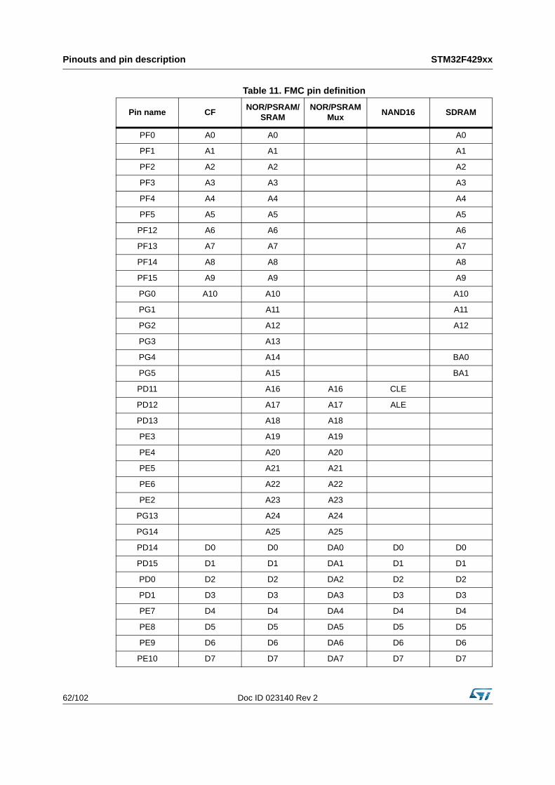
Pinouts and pin description STM32F429xx
62/102 Doc ID 023140 Rev 2
Table 11. FMC pin definition
Pin name CF NOR/PSRAM/SRAM
NOR/PSRAM Mux NAND16 SDRAM
PF0 A0 A0 A0
PF1 A1 A1 A1
PF2 A2 A2 A2
PF3 A3 A3 A3
PF4 A4 A4 A4
PF5 A5 A5 A5
PF12 A6 A6 A6
PF13 A7 A7 A7
PF14 A8 A8 A8
PF15 A9 A9 A9
PG0 A10 A10 A10
PG1 A11 A11
PG2 A12 A12
PG3 A13
PG4 A14 BA0
PG5 A15 BA1
PD11 A16 A16 CLE
PD12 A17 A17 ALE
PD13 A18 A18
PE3 A19 A19
PE4 A20 A20
PE5 A21 A21
PE6 A22 A22
PE2 A23 A23
PG13 A24 A24
PG14 A25 A25
PD14 D0 D0 DA0 D0 D0
PD15 D1 D1 DA1 D1 D1
PD0 D2 D2 DA2 D2 D2
PD1 D3 D3 DA3 D3 D3
PE7 D4 D4 DA4 D4 D4
PE8 D5 D5 DA5 D5 D5
PE9 D6 D6 DA6 D6 D6
PE10 D7 D7 DA7 D7 D7
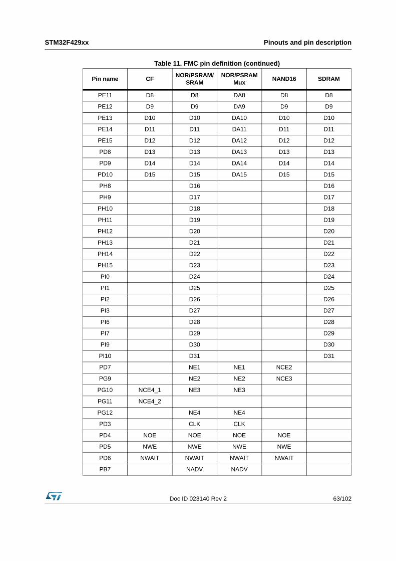
Doc ID 023140 Rev 2 63/102
STM32F429xx Pinouts and pin description
PE11 D8 D8 DA8 D8 D8
PE12 D9 D9 DA9 D9 D9
PE13 D10 D10 DA10 D10 D10
PE14 D11 D11 DA11 D11 D11
PE15 D12 D12 DA12 D12 D12
PD8 D13 D13 DA13 D13 D13
PD9 D14 D14 DA14 D14 D14
PD10 D15 D15 DA15 D15 D15
PH8 D16 D16
PH9 D17 D17
PH10 D18 D18
PH11 D19 D19
PH12 D20 D20
PH13 D21 D21
PH14 D22 D22
PH15 D23 D23
PI0 D24 D24
PI1 D25 D25
PI2 D26 D26
PI3 D27 D27
PI6 D28 D28
PI7 D29 D29
PI9 D30 D30
PI10 D31 D31
PD7 NE1 NE1 NCE2
PG9 NE2 NE2 NCE3
PG10 NCE4_1 NE3 NE3
PG11 NCE4_2
PG12 NE4 NE4
PD3 CLK CLK
PD4 NOE NOE NOE NOE
PD5 NWE NWE NWE NWE
PD6 NWAIT NWAIT NWAIT NWAIT
PB7 NADV NADV
Table 11. FMC pin definition (continued)
Pin name CF NOR/PSRAM/SRAM
NOR/PSRAM Mux NAND16 SDRAM

Pinouts and pin description STM32F429xx
64/102 Doc ID 023140 Rev 2
PF6 NIORD
PF7 NREG
PF8 NIOWR
PF9 CD
PF10 INTR
PG6 INT2
PG7 INT3
PE0 NBL0 NBL0 NBL0
PE1 NBL1 NBL1 NBL1
PI4 NBL2 NBL2
PI5 NBL3 NBL3
PG8 SDCLK
PC0 SDNWE
PF11 SDNRAS
PG15 SDNCAS
PH2 SDCKE0
PH3 SDNE0
PH6 SDNE1
PH7 SDCKE1
PH5 SDNWE
PC2 SDNE0
PC3 SDCKE0
PB5 SDCKE1
PB6 SDNE1
Table 11. FMC pin definition (continued)
Pin name CF NOR/PSRAM/SRAM
NOR/PSRAM Mux NAND16 SDRAM
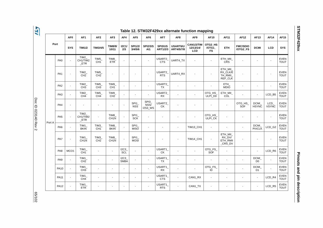
STM32F429xx
Pinouts and pin description
Doc ID
023140 Rev 2
65/102
Table 12. STM32F429xx alternate function mapping
Port
AF0 AF1 AF2 AF3 AF4 AF5 AF6 AF7 AF8 AF9 AF10 AF11 AF12 AF13 AF14 AF15
SYS TIM1/2 TIM3/4/5 TIM8/9/10/11
I2C1/2/3
SPI1/2/3/4/5/6
SPI2/3/SAI1
SPI3/USART1/2/3
USART6/UART4/5/7/8
CAN1/2/TIM12/13/14/
LCD
OTG2_HS/OTG1_
FSETH FMC/SDIO
/OTG2_FS DCMI LCD SYS
Port A
PA0 -TIM2_
CH1/TIM2_ETR
TIM5_CH1
TIM8_ETR - - - USART2_
CTS UART4_TX - - ETH_MII_CRS - - - EVEN
TOUT
PA1 - TIM2_CH2
TIM5_CH2 - - - - USART2_
RTS UART4_RX - -
ETH_MII_RX_CLK/ETH_RMII_REF_CLK
- - - EVENTOUT
PA2 - TIM2_CH3
TIM5_CH3
TIM9_CH1 - - - USART2_
TX - - - ETH_MDIO - - - EVEN
TOUT
PA3 - TIM2_CH4
TIM5_CH4
TIM9_CH2 - - - USART2_
RX - - OTG_HS_ULPI_D0
ETH_MII_COL - - LCD_B5 EVEN
TOUT
PA4 - - - - - SPI1_NSS
SPI3_NSS/
I2S3_WS
USART2_CK - - - - OTG_HS_
SOFDCMI_HSYNC
LCD_VSYNC
EVENTOUT
PA5 -TIM2_
CH1/TIM2_ETR
- TIM8_CH1N - SPI1_
SCK - - - - OTG_HS_ULPI_CK - - - - EVEN
TOUT
PA6 - TIM1_BKIN
TIM3_CH1
TIM8_BKIN - SPI1_
MISO - - - TIM13_CH1 - - - DCMI_PIXCLK LCD_G2 EVEN
TOUT
PA7 - TIM1_CH1N
TIM3_CH2
TIM8_CH1N - SPI1_
MOSI - - - TIM14_CH1 -
ETH_MII_RX_DV/
ETH_RMII_CRS_DV
- - - EVENTOUT
PA8 MCO1 TIM1_CH1 - - I2C3_
SCL - - USART1_CK - - OTG_FS_
SOF - - - LCD_R6 EVENTOUT
PA9 - TIM1_CH2 - - I2C3_
SMBA - - USART1_TX - - - - - DCMI_
D0 - EVENTOUT
PA10 - TIM1_CH3 - - - - - USART1_
RX - - OTG_FS_ID - - DCMI_
D1 - EVENTOUT
PA11 - TIM1_CH4 - - - - - USART1_
CTS - CAN1_RX - - - - LCD_R4 EVENTOUT
PA12 - TIM1_ETR - - - - - USART1_
RTS - CAN1_TX - - - - LCD_R5 EVENTOUT

Pinouts and pin descriptionSTM
32F429xx
66/102D
oc ID 023140 R
ev 2
Port A
PA13JTMS-SWDI
O- - - - - - - - - - - - - - EVEN
TOUT
PA14JTCK-SWCL
K- - - - - - - - - - - - - - EVEN
TOUT
PA15 JTDITIM2_
CH1/TIM2_ETR
- - - SPI1_NSS
SPI3_NSS/
I2S3_WS- - - - - - - - EVEN
TOUT
Port B
PB0 - TIM1_CH2N
TIM3_CH3
TIM8_CH2N - - - - - LCD_R3 OTG_HS_
ULPI_D1ETH_MII_
RXD2 - - - EVENTOUT
PB1 - TIM1_CH3N
TIM3_CH4
TIM8_CH3N - - - - - LCD_R6 OTG_HS_
ULPI_D2ETH_MII_
RXD3 - - - EVENTOUT
PB2 - - - - - - - - - - - - - - - EVENTOUT
PB3JTDO/TRACESWO
TIM2_CH2 - - - SPI1_
SCK
SPI3_SCK/
I2S3_CK- - - - - - - - EVEN
TOUT
PB4 NJTRST - TIM3_
CH1 - - SPI1_MISO
SPI3_MISO
I2S3ext_SD - - - - - - - EVEN
TOUT
PB5 - - TIM3_CH2 - I2C1_
SMBASPI1_MOSI
SPI3_MOSI/
I2S3_SD- - CAN2_RX OTG_HS_
ULPI_D7ETH_PPS
_OUTFMC_
SDCKE1DCMI_
D10 - EVENTOUT
PB6 - - TIM4_CH1 - I2C1_
SCL - - USART1_TX - CAN2_TX - - FMC_
SDNE1DCMI_
D5 - EVENTOUT
PB7 - - TIM4_CH2 - I2C1_
SDA - - USART1_RX - - - - FMC_NL DCMI_
VSYNC - EVENTOUT
PB8 - - TIM4_CH3
TIM10_CH1
I2C1_SCL - - - - CAN1_RX - ETH_MII_
TXD3 SDIO_D4 DCMI_D6 LCD_B6 EVEN
TOUT
PB9 - - TIM4_CH4
TIM11_CH1
I2C1_SDA
SPI2_NSS/I2S2_WS
- - - CAN1_TX - - SDIO_D5 DCMI_D7 LCD_B7 EVEN
TOUT
PB10 - TIM2_CH3 - - I2C2_
SCL
SPI2_SCK/I2S2_CK
- USART3_TX - - OTG_HS_
ULPI_D3ETH_MII_
RX_ER - - LCD_G4 EVENTOUT
Table 12. STM32F429xx alternate function mapping (continued)
Port
AF0 AF1 AF2 AF3 AF4 AF5 AF6 AF7 AF8 AF9 AF10 AF11 AF12 AF13 AF14 AF15
SYS TIM1/2 TIM3/4/5 TIM8/9/10/11
I2C1/2/3
SPI1/2/3/4/5/6
SPI2/3/SAI1
SPI3/USART1/2/3
USART6/UART4/5/7/8
CAN1/2/TIM12/13/14/
LCD
OTG2_HS/OTG1_
FSETH FMC/SDIO
/OTG2_FS DCMI LCD SYS
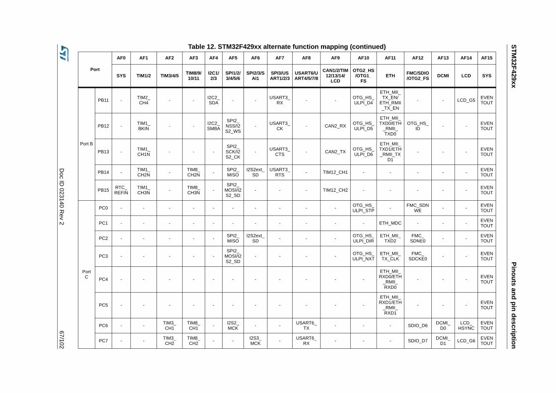
STM32F429xx
Pinouts and pin description
Doc ID
023140 Rev 2
67/102
Port B
PB11 - TIM2_CH4 - - I2C2_
SDA - - USART3_RX - - OTG_HS_
ULPI_D4
ETH_MII_TX_EN/
ETH_RMII_TX_EN
- - LCD_G5 EVENTOUT
PB12 - TIM1_BKIN - - I2C2_
SMBA
SPI2_NSS/I2S2_WS
- USART3_CK - CAN2_RX OTG_HS_
ULPI_D5
ETH_MII_TXD0/ETH
_RMII_TXD0
OTG_HS_ID - - EVEN
TOUT
PB13 - TIM1_CH1N - - -
SPI2_SCK/I2S2_CK
- USART3_CTS - CAN2_TX OTG_HS_
ULPI_D6
ETH_MII_TXD1/ETH_RMII_TX
D1
- - - EVENTOUT
PB14 - TIM1_CH2N - TIM8_
CH2N - SPI2_MISO
I2S2ext_SD
USART3_RTS - TIM12_CH1 - - - - - EVEN
TOUT
PB15 RTC_REFIN
TIM1_CH3N - TIM8_
CH3N -SPI2_
MOSI/I2S2_SD
- - - TIM12_CH2 - - - - - EVENTOUT
Port C
PC0 - - - - - - - - - - OTG_HS_ULPI_STP - FMC_SDN
WE - - EVENTOUT
PC1 - - - - - - - - - - - ETH_MDC - - - EVENTOUT
PC2 - - - - - SPI2_MISO
I2S2ext_SD - - - OTG_HS_
ULPI_DIRETH_MII_
TXD2FMC_
SDNE0 - - EVENTOUT
PC3 - - - - -SPI2_
MOSI/I2S2_SD
- - - - OTG_HS_ULPI_NXT
ETH_MII_TX_CLK
FMC_SDCKE0 - - EVEN
TOUT
PC4 - - - - - - - - - - -
ETH_MII_RXD0/ETH
_RMII_RXD0
- - - EVENTOUT
PC5 - - - - - - - - - - -
ETH_MII_RXD1/ETH
_RMII_RXD1
- - - EVENTOUT
PC6 - - TIM3_CH1
TIM8_CH1 - I2S2_
MCK - - USART6_TX - - - SDIO_D6 DCMI_
D0LCD_
HSYNCEVENTOUT
PC7 - - TIM3_CH2
TIM8_CH2 - - I2S3_
MCK - USART6_RX - - - SDIO_D7 DCMI_
D1 LCD_G6 EVENTOUT
Table 12. STM32F429xx alternate function mapping (continued)
Port
AF0 AF1 AF2 AF3 AF4 AF5 AF6 AF7 AF8 AF9 AF10 AF11 AF12 AF13 AF14 AF15
SYS TIM1/2 TIM3/4/5 TIM8/9/10/11
I2C1/2/3
SPI1/2/3/4/5/6
SPI2/3/SAI1
SPI3/USART1/2/3
USART6/UART4/5/7/8
CAN1/2/TIM12/13/14/
LCD
OTG2_HS/OTG1_
FSETH FMC/SDIO
/OTG2_FS DCMI LCD SYS
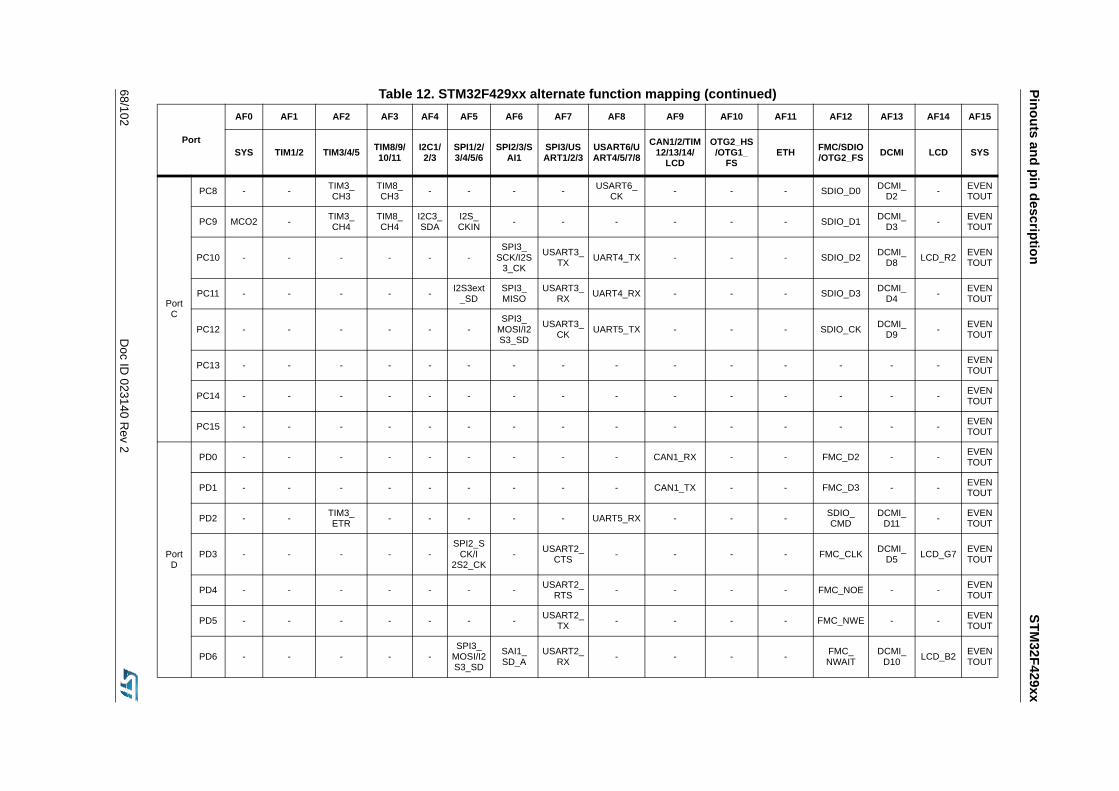
Pinouts and pin descriptionSTM
32F429xx
68/102D
oc ID 023140 R
ev 2
Port C
PC8 - - TIM3_CH3
TIM8_CH3 - - - - USART6_
CK - - - SDIO_D0 DCMI_D2 - EVEN
TOUT
PC9 MCO2 - TIM3_CH4
TIM8_CH4
I2C3_SDA
I2S_CKIN - - - - - - SDIO_D1 DCMI_
D3 - EVENTOUT
PC10 - - - - - -SPI3_
SCK/I2S3_CK
USART3_TX UART4_TX - - - SDIO_D2 DCMI_
D8 LCD_R2 EVENTOUT
PC11 - - - - - I2S3ext_SD
SPI3_MISO
USART3_RX UART4_RX - - - SDIO_D3 DCMI_
D4 - EVENTOUT
PC12 - - - - - -SPI3_
MOSI/I2S3_SD
USART3_CK UART5_TX - - - SDIO_CK DCMI_
D9 - EVENTOUT
PC13 - - - - - - - - - - - - - - - EVENTOUT
PC14 - - - - - - - - - - - - - - - EVENTOUT
PC15 - - - - - - - - - - - - - - - EVENTOUT
Port D
PD0 - - - - - - - - - CAN1_RX - - FMC_D2 - - EVENTOUT
PD1 - - - - - - - - - CAN1_TX - - FMC_D3 - - EVENTOUT
PD2 - - TIM3_ETR - - - - - UART5_RX - - - SDIO_
CMDDCMI_
D11 - EVENTOUT
PD3 - - - - -SPI2_S
CK/I2S2_CK
- USART2_CTS - - - - FMC_CLK DCMI_
D5 LCD_G7 EVENTOUT
PD4 - - - - - - - USART2_RTS - - - - FMC_NOE - - EVEN
TOUT
PD5 - - - - - - - USART2_TX - - - - FMC_NWE - - EVEN
TOUT
PD6 - - - - -SPI3_
MOSI/I2S3_SD
SAI1_SD_A
USART2_RX - - - - FMC_
NWAITDCMI_
D10 LCD_B2 EVENTOUT
Table 12. STM32F429xx alternate function mapping (continued)
Port
AF0 AF1 AF2 AF3 AF4 AF5 AF6 AF7 AF8 AF9 AF10 AF11 AF12 AF13 AF14 AF15
SYS TIM1/2 TIM3/4/5 TIM8/9/10/11
I2C1/2/3
SPI1/2/3/4/5/6
SPI2/3/SAI1
SPI3/USART1/2/3
USART6/UART4/5/7/8
CAN1/2/TIM12/13/14/
LCD
OTG2_HS/OTG1_
FSETH FMC/SDIO
/OTG2_FS DCMI LCD SYS

STM32F429xx
Pinouts and pin description
Doc ID
023140 Rev 2
69/102
Port D
PD7 - - - - - - - USART2_CK - - - -
FMC_NE1/FMC_NCE2
- - EVENTOUT
PD8 - - - - - - - USART3_TX - - - - FMC_D13 - - EVEN
TOUT
PD9 - - - - - - - USART3_RX - - - - FMC_D14 - - EVEN
TOUT
PD10 - - - - - - - USART3_CK - - - - FMC_D15 - LCD_B3 EVEN
TOUT
PD11 - - - - - - - USART3_CTS - - - - FMC_A16 - - EVEN
TOUT
PD12 - - TIM4_CH1 - - - - USART3_
RTS - - - - FMC_A17 - - EVENTOUT
PD13 - - TIM4_CH2 - - - - - - - - - FMC_A18 - - EVEN
TOUT
PD14 - - TIM4_CH3 - - - - - - - - - FMC_D0 - - EVEN
TOUT
PD15 - - TIM4_CH4 - - - - - - - - - FMC_D1 - - EVEN
TOUT
Port E
PE0 - - TIM4_ETR - - - - - UART8_Rx - - - FMC_
NBL0DCMI_
D2 - EVENTOUT
PE1 - - - - - - - - UART8_Tx - - - FMC_NBL1
DCMI_D3 - EVEN
TOUT
PE2 TRACECLK - - - - SPI4_
SCKSAI1_
MCLK_A - - - - ETH_MII_TXD3 FMC_A23 - - EVEN
TOUT
PE3 TRACED0 - - - - - SAI1_
SD_B - - - - - FMC_A19 - - EVENTOUT
PE4 TRACED1 - - - - SPI4_
NSSSAI1_FS_A - - - - - FMC_A20 DCMI_
D4 LCD_B0 EVENTOUT
PE5 TRACED2 - - TIM9_
CH1 - SPI4_MISO
SAI1_SCK_A - - - - - FMC_A21 DCMI_
D6 LCD_G0 EVENTOUT
PE6 TRACED3 - - TIM9_
CH2 - SPI4_MOSI
SAI1_SD_A - - - - - FMC_A22 DCMI_
D7 LCD_G1 EVENTOUT
Table 12. STM32F429xx alternate function mapping (continued)
Port
AF0 AF1 AF2 AF3 AF4 AF5 AF6 AF7 AF8 AF9 AF10 AF11 AF12 AF13 AF14 AF15
SYS TIM1/2 TIM3/4/5 TIM8/9/10/11
I2C1/2/3
SPI1/2/3/4/5/6
SPI2/3/SAI1
SPI3/USART1/2/3
USART6/UART4/5/7/8
CAN1/2/TIM12/13/14/
LCD
OTG2_HS/OTG1_
FSETH FMC/SDIO
/OTG2_FS DCMI LCD SYS
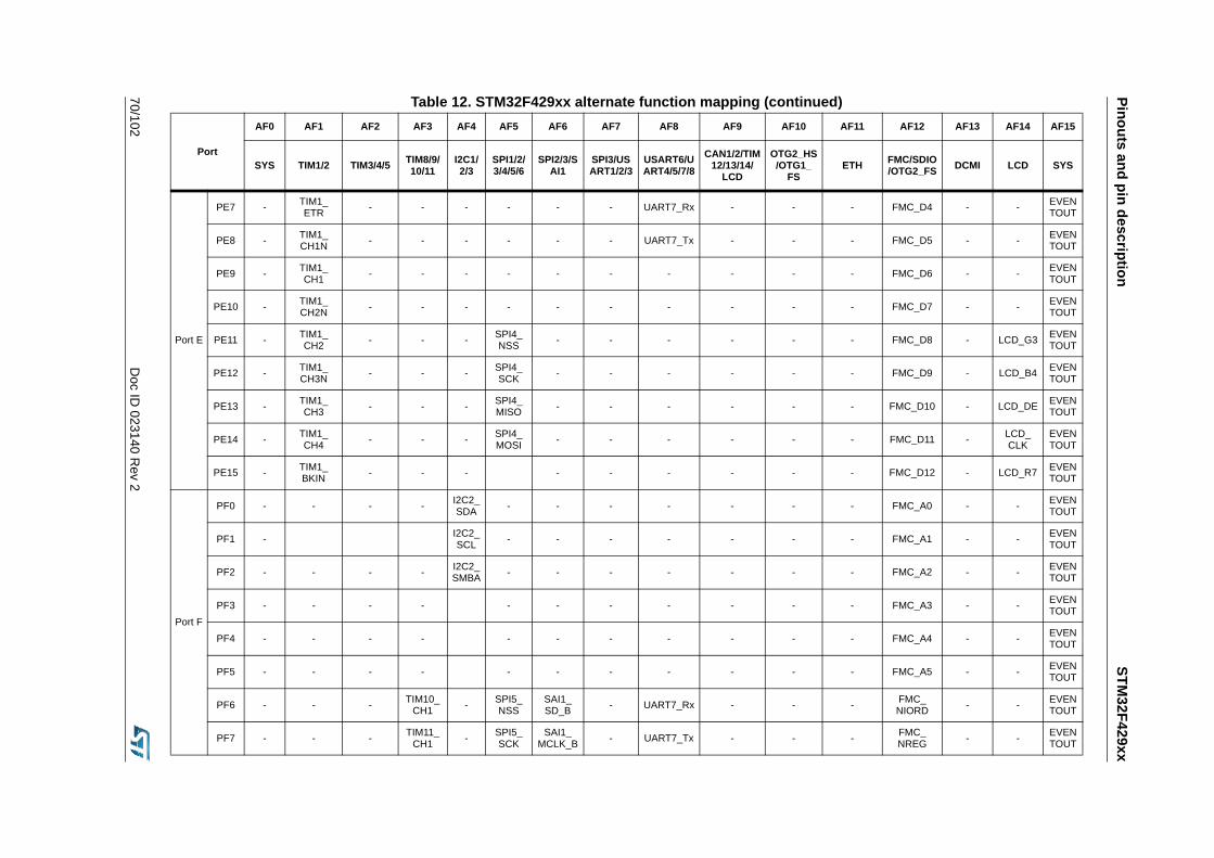
Pinouts and pin descriptionSTM
32F429xx
70/102D
oc ID 023140 R
ev 2
Port E
PE7 - TIM1_ETR - - - - - - UART7_Rx - - - FMC_D4 - - EVEN
TOUT
PE8 - TIM1_CH1N - - - - - - UART7_Tx - - - FMC_D5 - - EVEN
TOUT
PE9 - TIM1_CH1 - - - - - - - - - - FMC_D6 - - EVEN
TOUT
PE10 - TIM1_CH2N - - - - - - - - - - FMC_D7 - - EVEN
TOUT
PE11 - TIM1_CH2 - - - SPI4_
NSS - - - - - - FMC_D8 - LCD_G3 EVENTOUT
PE12 - TIM1_CH3N - - - SPI4_
SCK - - - - - - FMC_D9 - LCD_B4 EVENTOUT
PE13 - TIM1_CH3 - - - SPI4_
MISO - - - - - - FMC_D10 - LCD_DE EVENTOUT
PE14 - TIM1_CH4 - - - SPI4_
MOSI - - - - - - FMC_D11 - LCD_CLK
EVENTOUT
PE15 - TIM1_BKIN - - - - - - - - - FMC_D12 - LCD_R7 EVEN
TOUT
Port F
PF0 - - - - I2C2_SDA - - - - - - - FMC_A0 - - EVEN
TOUT
PF1 - I2C2_SCL - - - - - - - FMC_A1 - - EVEN
TOUT
PF2 - - - - I2C2_SMBA - - - - - - - FMC_A2 - - EVEN
TOUT
PF3 - - - - - - - - - - - FMC_A3 - - EVENTOUT
PF4 - - - - - - - - - - - FMC_A4 - - EVENTOUT
PF5 - - - - - - - - - - - FMC_A5 - - EVENTOUT
PF6 - - - TIM10_CH1 - SPI5_
NSSSAI1_SD_B - UART7_Rx - - - FMC_
NIORD - - EVENTOUT
PF7 - - - TIM11_CH1 - SPI5_
SCKSAI1_
MCLK_B - UART7_Tx - - - FMC_NREG - - EVEN
TOUT
Table 12. STM32F429xx alternate function mapping (continued)
Port
AF0 AF1 AF2 AF3 AF4 AF5 AF6 AF7 AF8 AF9 AF10 AF11 AF12 AF13 AF14 AF15
SYS TIM1/2 TIM3/4/5 TIM8/9/10/11
I2C1/2/3
SPI1/2/3/4/5/6
SPI2/3/SAI1
SPI3/USART1/2/3
USART6/UART4/5/7/8
CAN1/2/TIM12/13/14/
LCD
OTG2_HS/OTG1_
FSETH FMC/SDIO
/OTG2_FS DCMI LCD SYS
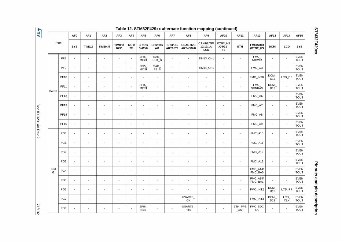
STM32F429xx
Pinouts and pin description
Doc ID
023140 Rev 2
71/102
Port F
PF8 - - - - - SPI5_MISO
SAI1_SCK_B - - TIM13_CH1 - - FMC_
NIOWR - - EVENTOUT
PF9 - - - - - SPI5_MOSI
SAI1_FS_B - - TIM14_CH1 - - FMC_CD - - EVEN
TOUT
PF10 - - - - - - - - - - - - FMC_INTR DCMI_D11 LCD_DE EVEN
TOUT
PF11 - - - - - SPI5_MOSI - - - - - - FMC_
SDNRASDCMI_
D12 - EVENTOUT
PF12 - - - - - - - - - - - - FMC_A6 - - EVENTOUT
PF13 - - - - - - - - - - - - FMC_A7 - - EVENTOUT
PF14 - - - - - - - - - - - - FMC_A8 - - EVENTOUT
PF15 - - - - - - - - - - - - FMC_A9 - - EVENTOUT
Port G
PG0 - - - - - - - - - - - - FMC_A10 - - EVENTOUT
PG1 - - - - - - - - - - - - FMC_A11 - - EVENTOUT
PG2 - - - - - - - - - - - - FMC_A12 - - EVENTOUT
PG3 - - - - - - - - - - - - FMC_A13 - - EVENTOUT
PG4 - - - - - - - - - - - - FMC_A14/FMC_BA0 - - EVEN
TOUT
PG5 - - - - - - - - - - - - FMC_A15/FMC_BA1 - - EVEN
TOUT
PG6 - - - - - - - - - - - - FMC_INT2 DCMI_D12 LCD_R7 EVEN
TOUT
PG7 - - - - - - - - USART6_CK - - - FMC_INT3 DCMI_
D13LCD_CLK
EVENTOUT
PG8 - - - - - SPI6_NSS - - USART6_
RTS - - ETH_PPS_OUT
FMC_SDCLK - - EVEN
TOUT
Table 12. STM32F429xx alternate function mapping (continued)
Port
AF0 AF1 AF2 AF3 AF4 AF5 AF6 AF7 AF8 AF9 AF10 AF11 AF12 AF13 AF14 AF15
SYS TIM1/2 TIM3/4/5 TIM8/9/10/11
I2C1/2/3
SPI1/2/3/4/5/6
SPI2/3/SAI1
SPI3/USART1/2/3
USART6/UART4/5/7/8
CAN1/2/TIM12/13/14/
LCD
OTG2_HS/OTG1_
FSETH FMC/SDIO
/OTG2_FS DCMI LCD SYS
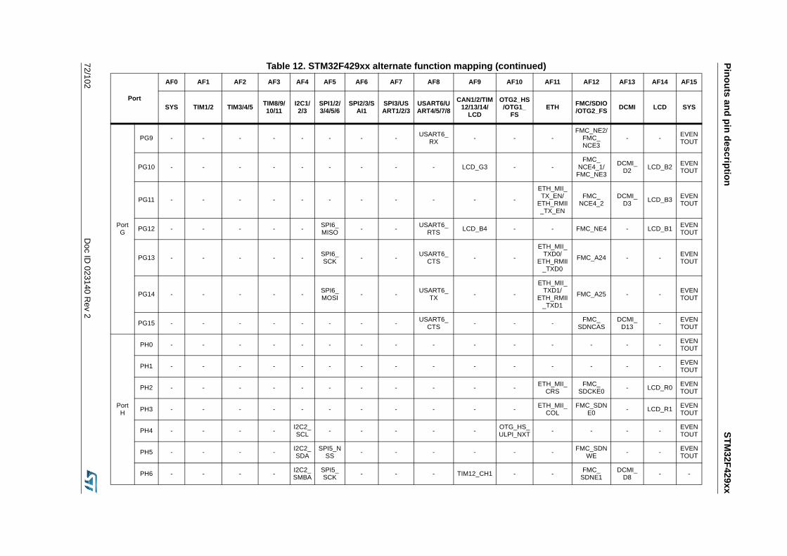
Pinouts and pin descriptionSTM
32F429xx
72/102D
oc ID 023140 R
ev 2
Port G
PG9 - - - - - - - - USART6_RX - - -
FMC_NE2/FMC_NCE3
- - EVENTOUT
PG10 - - - - - - - - - LCD_G3 - -FMC_
NCE4_1/FMC_NE3
DCMI_D2 LCD_B2 EVEN
TOUT
PG11 - - - - - - - - - - -
ETH_MII_TX_EN/
ETH_RMII_TX_EN
FMC_NCE4_2
DCMI_D3 LCD_B3 EVEN
TOUT
PG12 - - - - - SPI6_MISO - - USART6_
RTS LCD_B4 - - FMC_NE4 - LCD_B1 EVENTOUT
PG13 - - - - - SPI6_SCK - - USART6_
CTS - -
ETH_MII_TXD0/
ETH_RMII_TXD0
FMC_A24 - - EVENTOUT
PG14 - - - - - SPI6_MOSI - - USART6_
TX - -
ETH_MII_TXD1/
ETH_RMII_TXD1
FMC_A25 - - EVENTOUT
PG15 - - - - - - - - USART6_CTS - - - FMC_
SDNCASDCMI_
D13 - EVENTOUT
Port H
PH0 - - - - - - - - - - - - - - - EVENTOUT
PH1 - - - - - - - - - - - - - - - EVENTOUT
PH2 - - - - - - - - - - - ETH_MII_CRS
FMC_SDCKE0 - LCD_R0 EVEN
TOUT
PH3 - - - - - - - - - - - ETH_MII_COL
FMC_SDNE0 - LCD_R1 EVEN
TOUT
PH4 - - - - I2C2_SCL - - - - - OTG_HS_
ULPI_NXT - - - - EVENTOUT
PH5 - - - - I2C2_SDA
SPI5_NSS - - - - - - FMC_SDN
WE - - EVENTOUT
PH6 - - - - I2C2_SMBA
SPI5_SCK - - - TIM12_CH1 - - FMC_
SDNE1DCMI_
D8 - -
Table 12. STM32F429xx alternate function mapping (continued)
Port
AF0 AF1 AF2 AF3 AF4 AF5 AF6 AF7 AF8 AF9 AF10 AF11 AF12 AF13 AF14 AF15
SYS TIM1/2 TIM3/4/5 TIM8/9/10/11
I2C1/2/3
SPI1/2/3/4/5/6
SPI2/3/SAI1
SPI3/USART1/2/3
USART6/UART4/5/7/8
CAN1/2/TIM12/13/14/
LCD
OTG2_HS/OTG1_
FSETH FMC/SDIO
/OTG2_FS DCMI LCD SYS
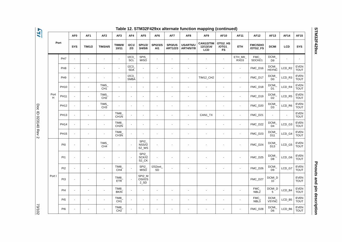
STM32F429xx
Pinouts and pin description
Doc ID
023140 Rev 2
73/102
Port H
PH7 - - - - I2C3_SCL
SPI5_MISO - - - - - ETH_MII_
RXD3FMC_
SDCKE1DCMI_
D9 - -
PH8 - - - - I2C3_SDA - - - - - - - FMC_D16 DCMI_
HSYNC LCD_R2 EVENTOUT
PH9 - - - - I2C3_SMBA - - - - TIM12_CH2 - - FMC_D17 DCMI_
D0 LCD_R3 EVENTOUT
PH10 - - TIM5_CH1 - - - - - - - - - FMC_D18 DCMI_
D1 LCD_R4 EVENTOUT
PH11 - - TIM5_CH2 - - - - - - - - - FMC_D19 DCMI_
D2 LCD_R5 EVENTOUT
PH12 - - TIM5_CH3 - - - - - - - - - FMC_D20 DCMI_
D3 LCD_R6 EVENTOUT
PH13 - - - TIM8_CH1N - - - - - CAN1_TX - - FMC_D21 - - EVEN
TOUT
PH14 - - - TIM8_CH2N - - - - - - - - FMC_D22 DCMI_
D4 LCD_G3 EVENTOUT
PH15 - - - TIM8_CH3N - - - - - - - - FMC_D23 DCMI_
D11 LCD_G4 EVENTOUT
Port I
PI0 - - TIM5_CH4 - -
SPI2_NSS/I2S2_WS
- - - - - - FMC_D24 DCMI_D13 LCD_G5 EVEN
TOUT
PI1 - - - - -SPI2_SCK/I2S2_CK
- - - - - - FMC_D25 DCMI_D8 LCD_G6 EVEN
TOUT
PI2 - - - TIM8_CH4 - SPI2_
MISOI2S2ext_
SD - - - - - FMC_D26 DCMI_D9 LCD_G7 EVEN
TOUT
PI3 - - - TIM8_ETR -
SPI2_MOSI/I2S2_SD
FMC_D27 DCMI_D10
EVENTOUT
PI4 - - - TIM8_BKIN - - - - - - - - FMC_
NBL2DCMI_D
5 LCD_B4 EVENTOUT
PI5 - - - TIM8_CH1 - - - - - - - - FMC_
NBL3DCMI_VSYNC LCD_B5 EVEN
TOUT
PI6 - - - TIM8_CH2 - - - - - - - - FMC_D28 DCMI_
D6 LCD_B6 EVENTOUT
Table 12. STM32F429xx alternate function mapping (continued)
Port
AF0 AF1 AF2 AF3 AF4 AF5 AF6 AF7 AF8 AF9 AF10 AF11 AF12 AF13 AF14 AF15
SYS TIM1/2 TIM3/4/5 TIM8/9/10/11
I2C1/2/3
SPI1/2/3/4/5/6
SPI2/3/SAI1
SPI3/USART1/2/3
USART6/UART4/5/7/8
CAN1/2/TIM12/13/14/
LCD
OTG2_HS/OTG1_
FSETH FMC/SDIO
/OTG2_FS DCMI LCD SYS
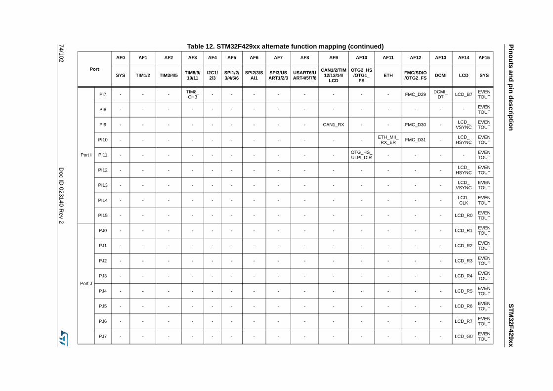
Pinouts and pin descriptionSTM
32F429xx
74/102D
oc ID 023140 R
ev 2
Port I
PI7 - - - TIM8_CH3 - - - - - - - - FMC_D29 DCMI_
D7 LCD_B7 EVENTOUT
PI8 - - - - - - - - - - - - - - - EVENTOUT
PI9 - - - - - - - - - CAN1_RX - - FMC_D30 - LCD_VSYNC
EVENTOUT
PI10 - - - - - - - - - - - ETH_MII_RX_ER FMC_D31 - LCD_
HSYNCEVENTOUT
PI11 - - - - - - - - - - OTG_HS_ULPI_DIR - - - - EVEN
TOUT
PI12 - - - - - - - - - - - - - - LCD_HSYNC
EVENTOUT
PI13 - - - - - - - - - - - - - - LCD_VSYNC
EVENTOUT
PI14 - - - - - - - - - - - - - - LCD_CLK
EVENTOUT
PI15 - - - - - - - - - - - - - - LCD_R0 EVENTOUT
Port J
PJ0 - - - - - - - - - - - - - - LCD_R1 EVENTOUT
PJ1 - - - - - - - - - - - - - - LCD_R2 EVENTOUT
PJ2 - - - - - - - - - - - - - - LCD_R3 EVENTOUT
PJ3 - - - - - - - - - - - - - - LCD_R4 EVENTOUT
PJ4 - - - - - - - - - - - - - - LCD_R5 EVENTOUT
PJ5 - - - - - - - - - - - - - - LCD_R6 EVENTOUT
PJ6 - - - - - - - - - - - - - - LCD_R7 EVENTOUT
PJ7 - - - - - - - - - - - - - - LCD_G0 EVENTOUT
Table 12. STM32F429xx alternate function mapping (continued)
Port
AF0 AF1 AF2 AF3 AF4 AF5 AF6 AF7 AF8 AF9 AF10 AF11 AF12 AF13 AF14 AF15
SYS TIM1/2 TIM3/4/5 TIM8/9/10/11
I2C1/2/3
SPI1/2/3/4/5/6
SPI2/3/SAI1
SPI3/USART1/2/3
USART6/UART4/5/7/8
CAN1/2/TIM12/13/14/
LCD
OTG2_HS/OTG1_
FSETH FMC/SDIO
/OTG2_FS DCMI LCD SYS
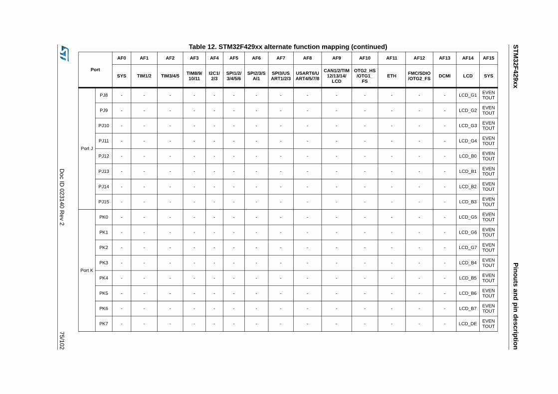
STM32F429xx
Pinouts and pin description
Doc ID
023140 Rev 2
75/102
Port J
PJ8 - - - - - - - - - - - - - - LCD_G1 EVENTOUT
PJ9 - - - - - - - - - - - - - - LCD_G2 EVENTOUT
PJ10 - - - - - - - - - - - - - - LCD_G3 EVENTOUT
PJ11 - - - - - - - - - - - - - - LCD_G4 EVENTOUT
PJ12 - - - - - - - - - - - - - - LCD_B0 EVENTOUT
PJ13 - - - - - - - - - - - - - - LCD_B1 EVENTOUT
PJ14 - - - - - - - - - - - - - - LCD_B2 EVENTOUT
PJ15 - - - - - - - - - - - - - - LCD_B3 EVENTOUT
Port K
PK0 - - - - - - - - - - - - - - LCD_G5 EVENTOUT
PK1 - - - - - - - - - - - - - - LCD_G6 EVENTOUT
PK2 - - - - - - - - - - - - - - LCD_G7 EVENTOUT
PK3 - - - - - - - - - - - - - - LCD_B4 EVENTOUT
PK4 - - - - - - - - - - - - - - LCD_B5 EVENTOUT
PK5 - - - - - - - - - - - - - - LCD_B6 EVENTOUT
PK6 - - - - - - - - - - - - - - LCD_B7 EVENTOUT
PK7 - - - - - - - - - - - - - - LCD_DE EVENTOUT
Table 12. STM32F429xx alternate function mapping (continued)
Port
AF0 AF1 AF2 AF3 AF4 AF5 AF6 AF7 AF8 AF9 AF10 AF11 AF12 AF13 AF14 AF15
SYS TIM1/2 TIM3/4/5 TIM8/9/10/11
I2C1/2/3
SPI1/2/3/4/5/6
SPI2/3/SAI1
SPI3/USART1/2/3
USART6/UART4/5/7/8
CAN1/2/TIM12/13/14/
LCD
OTG2_HS/OTG1_
FSETH FMC/SDIO
/OTG2_FS DCMI LCD SYS
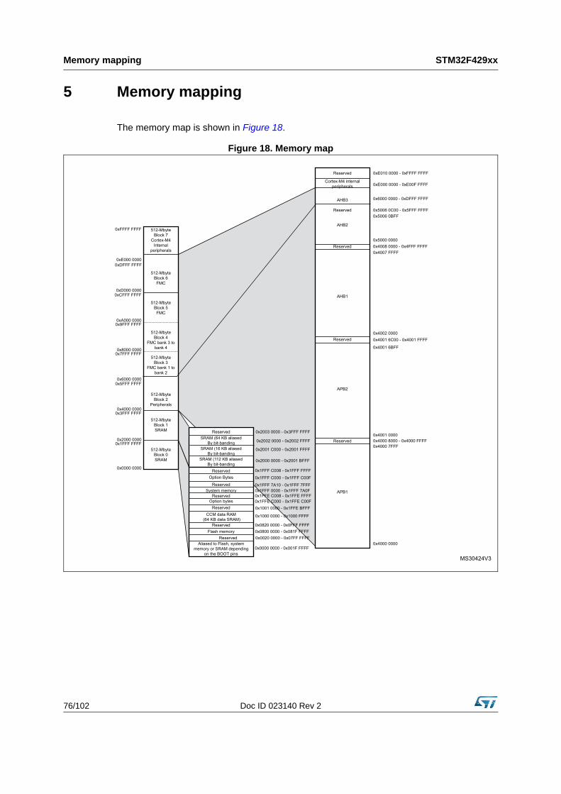
Memory mapping STM32F429xx
76/102 Doc ID 023140 Rev 2
5 Memory mapping
The memory map is shown in Figure 18.
Figure 18. Memory map
MS30424V3
512-MbyteBlock 7
Cortex-M4Internal
peripherals
512-MbyteBlock 6
FMC
512-MbyteBlock 4
FMC bank 3 to bank 4
0x0000 0000
0x1FFF FFFF0x2000 0000
0x3FFF FFFF0x4000 0000
0x5FFF FFFF0x6000 0000
0x7FFF FFFF0x8000 0000
0x9FFF FFFF0xA000 0000
0xCFFF FFFF0xD000 0000
0xDFFF FFFF0xE000 0000
0xFFFF FFFF
SRAM (16 KB aliasedBy bit-banding
Reserved
0x2000 0000 - 0x2001 BFFF
0x2001 C000 - 0x2001 FFFF
0x2003 0000 - 0x3FFF FFFF
0x4000 0000
Reserved0x4000 7FFF0x4000 8000 - 0x4000 FFFF0x4001 0000
Reserved 0x5006 0C00 - 0x5FFF FFFF
AHB3 0x6000 0000 - 0xDFFF FFFF
AHB2
SRAM (112 KB aliasedBy bit-banding
0x5006 0BFF
0x5000 0000
SRAM (64 KB aliasedBy bit-banding 0x2002 0000 - 0x2002 FFFF
APB1
APB2
0x4001 6BFF
0x4001 6C00 - 0x4001 FFFFReserved
0x4008 0000 - 0x4FFF FFFF0x4007 FFFF
AHB1
Reserved
Flash memory0x0820 0000 - 0x0FFF FFFF
0x1FFF 0000 - 0x1FFF 7A0F
0x1FFF C000 - 0x1FFF C00F
0x0800 0000 - 0x081F FFFF 0x0020 0000 - 0x07FF FFFF
0x0000 0000 - 0x001F FFFF
System memory
Reserved
ReservedAliased to Flash, system
memory or SRAM dependingon the BOOT pins
Option BytesReserved 0x1FFF C008 - 0x1FFF FFFF
0x1FFF 7A10 - 0x1FFF 7FFFReserved
CCM data RAM (64 KB data SRAM)
0x1000 0000 - 0x1000 FFFF
Reserved 0x1001 0000 - 0x1FFE BFFF0x1FFE C000 - 0x1FFE C00FOption bytes
Reserved 0x1FFE C008 - 0x1FFE FFFF
0x4002 0000
Cortex-M4 internal peripherals 0xE000 0000 - 0xE00F FFFF
Reserved 0xE010 0000 - 0xFFFF FFFF
512-MbyteBlock 5
FMC
512-MbyteBlock 3
FMC bank 1 to bank 2
512-MbyteBlock 2
Peripherals
512-MbyteBlock 1SRAM
512-MbyteBlock 0SRAM
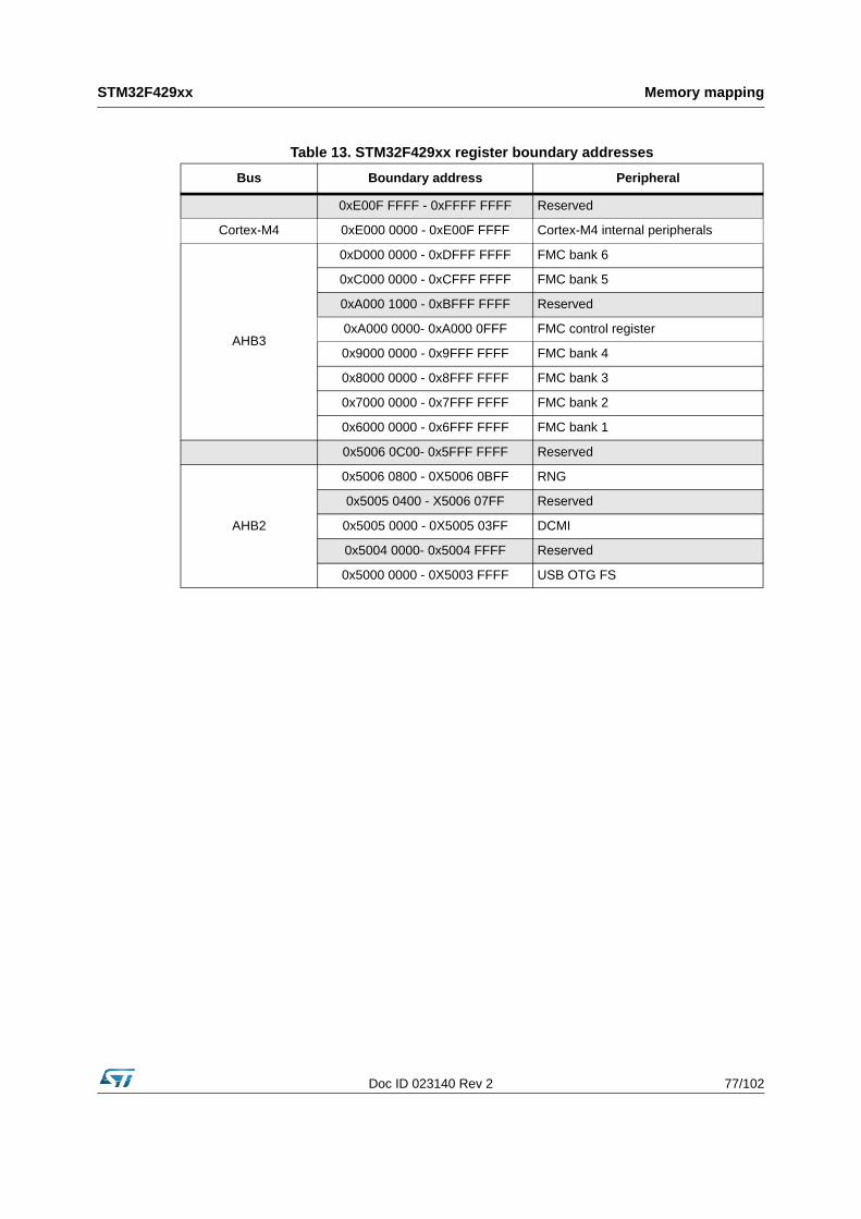
Doc ID 023140 Rev 2 77/102
STM32F429xx Memory mapping
Table 13. STM32F429xx register boundary addresses
Bus Boundary address Peripheral
0xE00F FFFF - 0xFFFF FFFF Reserved
Cortex-M4 0xE000 0000 - 0xE00F FFFF Cortex-M4 internal peripherals
AHB3
0xD000 0000 - 0xDFFF FFFF FMC bank 6
0xC000 0000 - 0xCFFF FFFF FMC bank 5
0xA000 1000 - 0xBFFF FFFF Reserved
0xA000 0000- 0xA000 0FFF FMC control register
0x9000 0000 - 0x9FFF FFFF FMC bank 4
0x8000 0000 - 0x8FFF FFFF FMC bank 3
0x7000 0000 - 0x7FFF FFFF FMC bank 2
0x6000 0000 - 0x6FFF FFFF FMC bank 1
0x5006 0C00- 0x5FFF FFFF Reserved
AHB2
0x5006 0800 - 0X5006 0BFF RNG
0x5005 0400 - X5006 07FF Reserved
0x5005 0000 - 0X5005 03FF DCMI
0x5004 0000- 0x5004 FFFF Reserved
0x5000 0000 - 0X5003 FFFF USB OTG FS
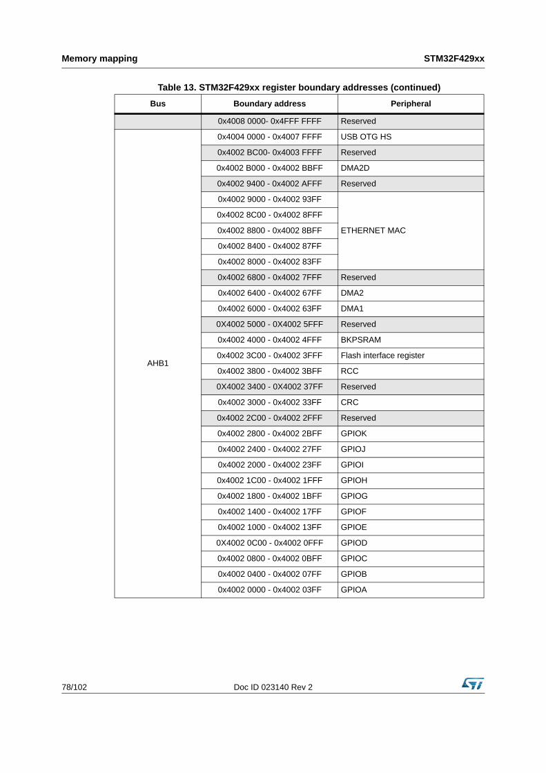
Memory mapping STM32F429xx
78/102 Doc ID 023140 Rev 2
0x4008 0000- 0x4FFF FFFF Reserved
AHB1
0x4004 0000 - 0x4007 FFFF USB OTG HS
0x4002 BC00- 0x4003 FFFF Reserved
0x4002 B000 - 0x4002 BBFF DMA2D
0x4002 9400 - 0x4002 AFFF Reserved
0x4002 9000 - 0x4002 93FF
ETHERNET MAC
0x4002 8C00 - 0x4002 8FFF
0x4002 8800 - 0x4002 8BFF
0x4002 8400 - 0x4002 87FF
0x4002 8000 - 0x4002 83FF
0x4002 6800 - 0x4002 7FFF Reserved
0x4002 6400 - 0x4002 67FF DMA2
0x4002 6000 - 0x4002 63FF DMA1
0X4002 5000 - 0X4002 5FFF Reserved
0x4002 4000 - 0x4002 4FFF BKPSRAM
0x4002 3C00 - 0x4002 3FFF Flash interface register
0x4002 3800 - 0x4002 3BFF RCC
0X4002 3400 - 0X4002 37FF Reserved
0x4002 3000 - 0x4002 33FF CRC
0x4002 2C00 - 0x4002 2FFF Reserved
0x4002 2800 - 0x4002 2BFF GPIOK
0x4002 2400 - 0x4002 27FF GPIOJ
0x4002 2000 - 0x4002 23FF GPIOI
0x4002 1C00 - 0x4002 1FFF GPIOH
0x4002 1800 - 0x4002 1BFF GPIOG
0x4002 1400 - 0x4002 17FF GPIOF
0x4002 1000 - 0x4002 13FF GPIOE
0X4002 0C00 - 0x4002 0FFF GPIOD
0x4002 0800 - 0x4002 0BFF GPIOC
0x4002 0400 - 0x4002 07FF GPIOB
0x4002 0000 - 0x4002 03FF GPIOA
Table 13. STM32F429xx register boundary addresses (continued)
Bus Boundary address Peripheral
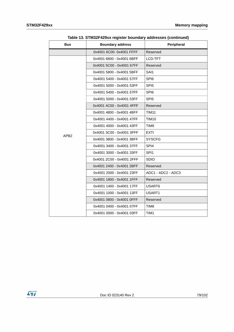
Doc ID 023140 Rev 2 79/102
STM32F429xx Memory mapping
0x4001 6C00- 0x4001 FFFF Reserved
APB2
0x4001 6800 - 0x4001 6BFF LCD-TFT
0x4001 5C00 - 0x4001 67FF Reserved
0x4001 5800 - 0x4001 5BFF SAI1
0x4001 5400 - 0x4001 57FF SPI6
0x4001 5000 - 0x4001 53FF SPI5
0x4001 5400 - 0x4001 57FF SPI6
0x4001 5000 - 0x4001 53FF SPI5
0x4001 4C00 - 0x4001 4FFF Reserved
0x4001 4800 - 0x4001 4BFF TIM11
0x4001 4400 - 0x4001 47FF TIM10
0x4001 4000 - 0x4001 43FF TIM9
0x4001 3C00 - 0x4001 3FFF EXTI
0x4001 3800 - 0x4001 3BFF SYSCFG
0x4001 3400 - 0x4001 37FF SPI4
0x4001 3000 - 0x4001 33FF SPI1
0x4001 2C00 - 0x4001 2FFF SDIO
0x4001 2400 - 0x4001 2BFF Reserved
0x4001 2000 - 0x4001 23FF ADC1 - ADC2 - ADC3
0x4001 1800 - 0x4001 1FFF Reserved
0x4001 1400 - 0x4001 17FF USART6
0x4001 1000 - 0x4001 13FF USART1
0x4001 0800 - 0x4001 0FFF Reserved
0x4001 0400 - 0x4001 07FF TIM8
0x4001 0000 - 0x4001 03FF TIM1
Table 13. STM32F429xx register boundary addresses (continued)
Bus Boundary address Peripheral
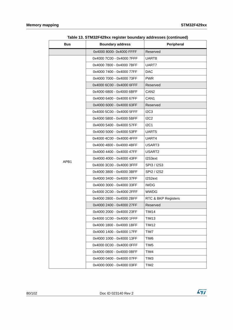
Memory mapping STM32F429xx
80/102 Doc ID 023140 Rev 2
0x4000 8000- 0x4000 FFFF Reserved
APB1
0x4000 7C00 - 0x4000 7FFF UART8
0x4000 7800 - 0x4000 7BFF UART7
0x4000 7400 - 0x4000 77FF DAC
0x4000 7000 - 0x4000 73FF PWR
0x4000 6C00 - 0x4000 6FFF Reserved
0x4000 6800 - 0x4000 6BFF CAN2
0x4000 6400 - 0x4000 67FF CAN1
0x4000 6000 - 0x4000 63FF Reserved
0x4000 5C00 - 0x4000 5FFF I2C3
0x4000 5800 - 0x4000 5BFF I2C2
0x4000 5400 - 0x4000 57FF I2C1
0x4000 5000 - 0x4000 53FF UART5
0x4000 4C00 - 0x4000 4FFF UART4
0x4000 4800 - 0x4000 4BFF USART3
0x4000 4400 - 0x4000 47FF USART2
0x4000 4000 - 0x4000 43FF I2S3ext
0x4000 3C00 - 0x4000 3FFF SPI3 / I2S3
0x4000 3800 - 0x4000 3BFF SPI2 / I2S2
0x4000 3400 - 0x4000 37FF I2S2ext
0x4000 3000 - 0x4000 33FF IWDG
0x4000 2C00 - 0x4000 2FFF WWDG
0x4000 2800 - 0x4000 2BFF RTC & BKP Registers
0x4000 2400 - 0x4000 27FF Reserved
0x4000 2000 - 0x4000 23FF TIM14
0x4000 1C00 - 0x4000 1FFF TIM13
0x4000 1800 - 0x4000 1BFF TIM12
0x4000 1400 - 0x4000 17FF TIM7
0x4000 1000 - 0x4000 13FF TIM6
0x4000 0C00 - 0x4000 0FFF TIM5
0x4000 0800 - 0x4000 0BFF TIM4
0x4000 0400 - 0x4000 07FF TIM3
0x4000 0000 - 0x4000 03FF TIM2
Table 13. STM32F429xx register boundary addresses (continued)
Bus Boundary address Peripheral
Doc ID 023140 Rev 2 81/102
STM32F429xx Package characteristics
6 Package characteristics
6.1 Package mechanical dataIn order to meet environmental requirements, ST offers these devices in different grades of ECOPACK® packages, depending on their level of environmental compliance. ECOPACK® specifications, grade definitions and product status are available at: www.st.com. ECOPACK® is an ST trademark.
Figure 19. LQFP100, 14 x 14 mm 100-pin low-profile quad flat package outline
1. Drawing is not to scale.
Package characteristics STM32F429xx
82/102 Doc ID 023140 Rev 2
Table 14. LQPF100, 14 x 14 mm 100-pin low-profile quad flat package mechanical data
Symbolmillimeters inches(1)
Min Typ Max Min Typ Max
A 1.600 0.0630
A1 0.050 0.150 0.0020 0.0059
A2 1.350 1.400 1.450 0.0531 0.0551 0.0571
b 0.170 0.220 0.270 0.0067 0.0087 0.0106
c 0.090 0.200 0.0035 0.0079
D 15.800 16.000 16.200 0.6220 0.6299 0.6378
D1 13.800 14.000 14.200 0.5433 0.5512 0.5591
D3 12.000 0.4724
E 15.800 16.000 16.200 0.6220 0.6299 0.6378
E1 13.800 14.000 14.200 0.5433 0.5512 0.5591
E3 12.000 0.4724
e 0.500 0.0197
L 0.450 0.600 0.750 0.0177 0.0236 0.0295
L1 1.000 0.0394
k 0° 3.5° 7° 0° 3.5° 7°
ccc 0.080 0.0031
1. Values in inches are converted from mm and rounded to 4 decimal digits.
Doc ID 023140 Rev 2 83/102
STM32F429xx Package characteristics
Figure 20. LQPF100 recommended footprint
1. Dimensions are expressed in millimeters.
Package characteristics STM32F429xx
84/102 Doc ID 023140 Rev 2
Figure 21. WLCSP143, 0.4 mm pitch wafe level chip scale package outline
1. Drawing is not to scale.

Doc ID 023140 Rev 2 85/102
STM32F429xx Package characteristics
Table 15. WLCSP143, 0.4 mm pitch wafe level chip scale package mechanical data
Symbolmillimeters inches(1)
Min Typ Max Min Typ Max
A 0.525 0.555 0.585 0.0207 0.0219 0.0230
A1 - 0.175 - - 0.0069 -
A2 - 0.380 - - 0.0150 -
A3 0.220 0.025 0.280 0.0087 0.0010 0.0110
b - 0.250° - - 0.250° -
D 4.486 4.521 4.556 0.1766 0.1780 0.1794
E 5.512 5.547 5.582 0.2170 0.2184 0.2198
e - 0.400 - - 0.0157 -
e1 - 4.000 - - 0.1575 -
e2 - 4.800 - - 0.1890 -
F - 0.261 - - 0.0103 -
G - 0.374 - - 0.0147 -
eee - 0.050 - - 0.0020 -
1. Values in inches are converted from mm and rounded to 4 decimal digits.
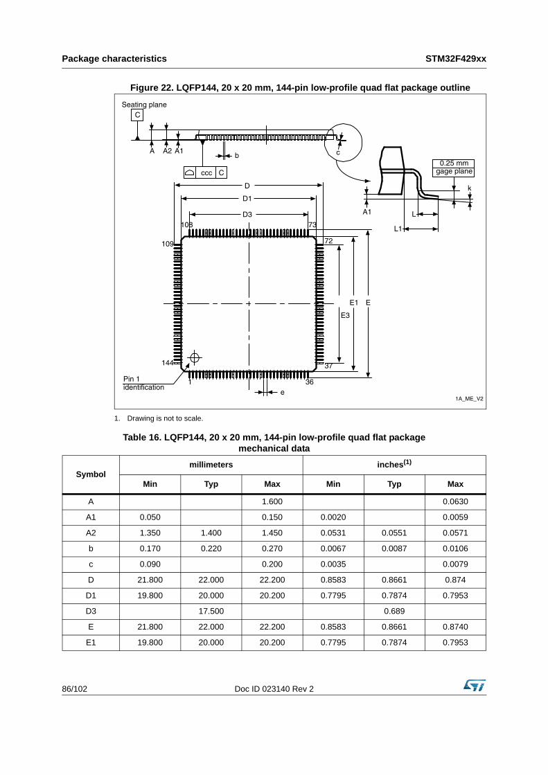
Package characteristics STM32F429xx
86/102 Doc ID 023140 Rev 2
Figure 22. LQFP144, 20 x 20 mm, 144-pin low-profile quad flat package outline
1. Drawing is not to scale.
Table 16. LQFP144, 20 x 20 mm, 144-pin low-profile quad flat package mechanical data
Symbolmillimeters inches(1)
Min Typ Max Min Typ Max
A 1.600 0.0630
A1 0.050 0.150 0.0020 0.0059
A2 1.350 1.400 1.450 0.0531 0.0551 0.0571
b 0.170 0.220 0.270 0.0067 0.0087 0.0106
c 0.090 0.200 0.0035 0.0079
D 21.800 22.000 22.200 0.8583 0.8661 0.874
D1 19.800 20.000 20.200 0.7795 0.7874 0.7953
D3 17.500 0.689
E 21.800 22.000 22.200 0.8583 0.8661 0.8740
E1 19.800 20.000 20.200 0.7795 0.7874 0.7953

Doc ID 023140 Rev 2 87/102
STM32F429xx Package characteristics
Figure 23. LQFP144 recommended footprint
1. Dimensions are expressed in millimeters.
E3 17.500 0.6890
e 0.500 0.0197
L 0.450 0.600 0.750 0.0177 0.0236 0.0295
L1 1.000 0.0394
k 0° 3.5° 7° 0° 3.5° 7°
ccc 0.080 0.0031
1. Values in inches are converted from mm and rounded to 4 decimal digits.
Table 16. LQFP144, 20 x 20 mm, 144-pin low-profile quad flat package mechanical data (continued)
Symbolmillimeters inches(1)
Min Typ Max Min Typ Max
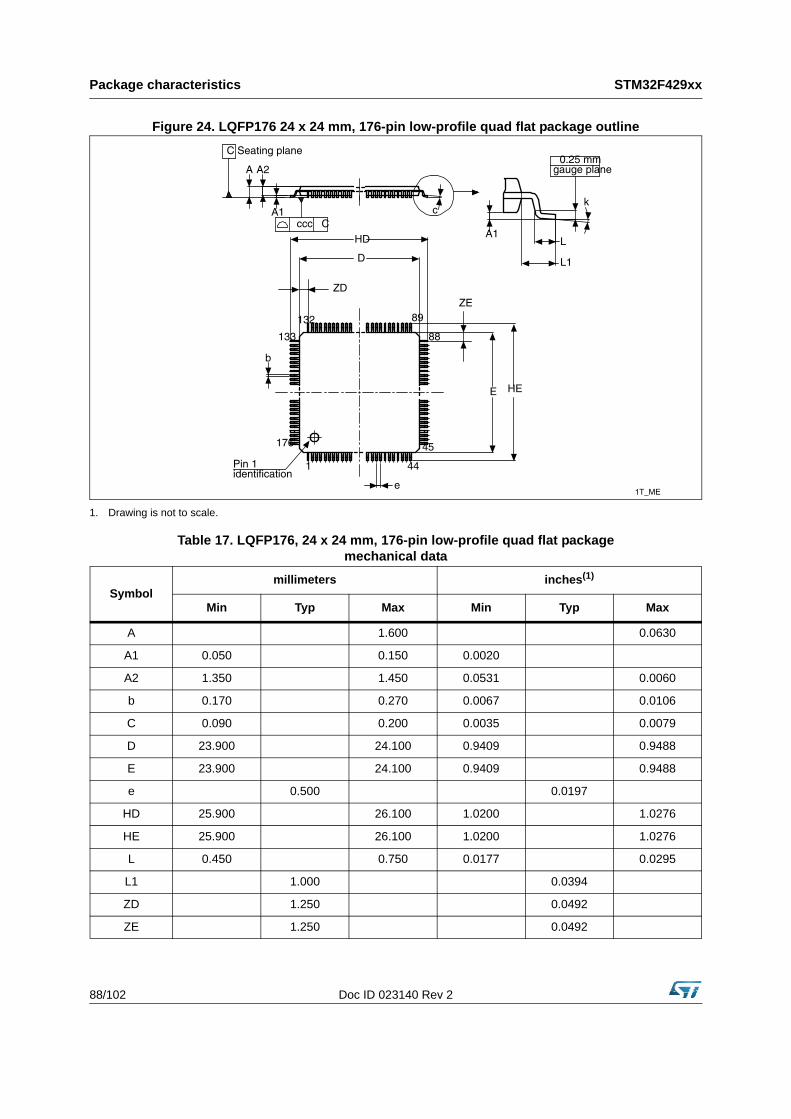
Package characteristics STM32F429xx
88/102 Doc ID 023140 Rev 2
Figure 24. LQFP176 24 x 24 mm, 176-pin low-profile quad flat package outline
1. Drawing is not to scale.
Table 17. LQFP176, 24 x 24 mm, 176-pin low-profile quad flat package mechanical data
Symbolmillimeters inches(1)
Min Typ Max Min Typ Max
A 1.600 0.0630
A1 0.050 0.150 0.0020
A2 1.350 1.450 0.0531 0.0060
b 0.170 0.270 0.0067 0.0106
C 0.090 0.200 0.0035 0.0079
D 23.900 24.100 0.9409 0.9488
E 23.900 24.100 0.9409 0.9488
e 0.500 0.0197
HD 25.900 26.100 1.0200 1.0276
HE 25.900 26.100 1.0200 1.0276
L 0.450 0.750 0.0177 0.0295
L1 1.000 0.0394
ZD 1.250 0.0492
ZE 1.250 0.0492
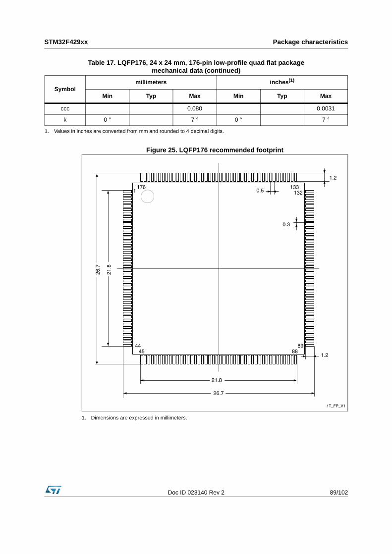
Doc ID 023140 Rev 2 89/102
STM32F429xx Package characteristics
Figure 25. LQFP176 recommended footprint
1. Dimensions are expressed in millimeters.
ccc 0.080 0.0031
k 0 ° 7 ° 0 ° 7 °
1. Values in inches are converted from mm and rounded to 4 decimal digits.
Table 17. LQFP176, 24 x 24 mm, 176-pin low-profile quad flat package mechanical data (continued)
Symbolmillimeters inches(1)
Min Typ Max Min Typ Max
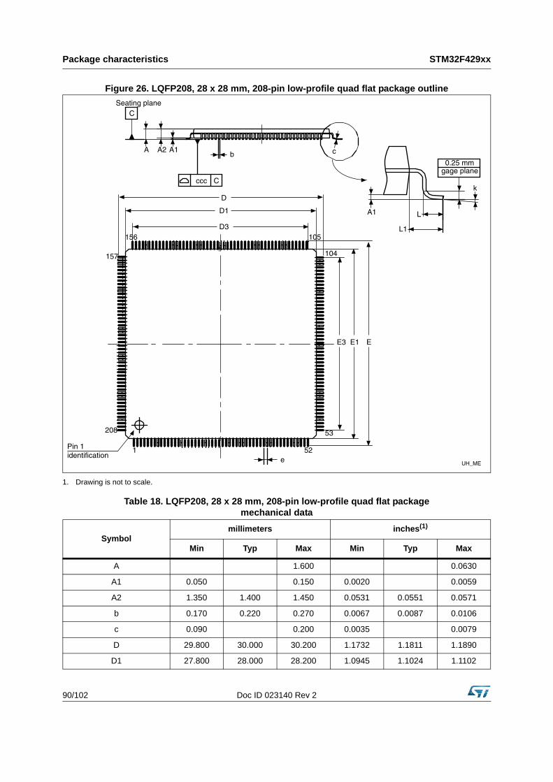
Package characteristics STM32F429xx
90/102 Doc ID 023140 Rev 2
Figure 26. LQFP208, 28 x 28 mm, 208-pin low-profile quad flat package outline
1. Drawing is not to scale.
Table 18. LQFP208, 28 x 28 mm, 208-pin low-profile quad flat package mechanical data
Symbolmillimeters inches(1)
Min Typ Max Min Typ Max
A 1.600 0.0630
A1 0.050 0.150 0.0020 0.0059
A2 1.350 1.400 1.450 0.0531 0.0551 0.0571
b 0.170 0.220 0.270 0.0067 0.0087 0.0106
c 0.090 0.200 0.0035 0.0079
D 29.800 30.000 30.200 1.1732 1.1811 1.1890
D1 27.800 28.000 28.200 1.0945 1.1024 1.1102

Doc ID 023140 Rev 2 91/102
STM32F429xx Package characteristics
Figure 27. LQFP208 recommended footprint
1. Dimensions are expressed in millimeters.
D3 25.500 1.0039
E 29.800 30.000 30.200 1.1732 1.1811 1.1890
E1 27.800 28.000 28.200 1.0945 1.1024 1.1102
E3 25.500 1.0039
e 0.500 0.0197
L 0.450 0.600 0.750 0.0177 0.0236 0.0295
L1 1.000 0.0394
k 0° 3.5° 7.0° 0° 3.5° 7.0°
ccc 0.080 0.0031
1. Values in inches are converted from mm and rounded to 4 decimal digits.
Table 18. LQFP208, 28 x 28 mm, 208-pin low-profile quad flat package mechanical data (continued)
Symbolmillimeters inches(1)
Min Typ Max Min Typ Max
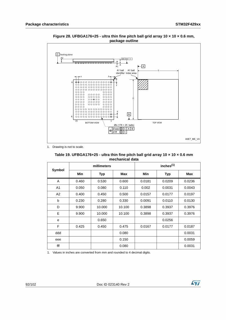
Package characteristics STM32F429xx
92/102 Doc ID 023140 Rev 2
Figure 28. UFBGA176+25 - ultra thin fine pitch ball grid array 10 × 10 × 0.6 mm,package outline
1. Drawing is not to scale.
Table 19. UFBGA176+25 - ultra thin fine pitch ball grid array 10 × 10 × 0.6 mmmechanical data
Symbolmillimeters inches(1)
1. Values in inches are converted from mm and rounded to 4 decimal digits.
Min Typ Max Min Typ Max
A 0.460 0.530 0.600 0.0181 0.0209 0.0236
A1 0.050 0.080 0.110 0.002 0.0031 0.0043
A2 0.400 0.450 0.500 0.0157 0.0177 0.0197
b 0.230 0.280 0.330 0.0091 0.0110 0.0130
D 9.900 10.000 10.100 0.3898 0.3937 0.3976
E 9.900 10.000 10.100 0.3898 0.3937 0.3976
e 0.650 0.0256
F 0.425 0.450 0.475 0.0167 0.0177 0.0187
ddd 0.080 0.0031
eee 0.150 0.0059
fff 0.080 0.0031
A0E7_ME_V4
Seating planeA2 Cddd
A1A
e F
F
e
R
A
15 1BOTTOM VIEW
E
D
TOP VIEWØb (176 + 25 balls)
B
A
BeeeØ MfffØ M
CC
A
C
A1 ball identifier
A1 ball index area

Doc ID 023140 Rev 2 93/102
STM32F429xx Package characteristics
Figure 29. TFBGA216 - ultra thin fine pitch ball grid array 13 × 13 × 0.8mm,package outline
1. Drawing is not to scale.
A0L2_ME_V2
Seating plane
A1
e F
F
D
R
Øb (216 balls)
A
E
TOP VIEWBOTTOM VIEW115
e
AA2
Y
X
Z
ddd Z
D1
E1
eee Z Y Xfff
ØØ
MM Z
A1 ball identifier
A1 ball index area
Table 20. TFBGA216 - ultra thin fine pitch ball grid array 13 × 13 × 0.8mmpackage mechanical data
Symbolmillimeters inches(1)
Min Typ Max Min Typ Max
A 1.100 0.0433
A1 0.150 0.0059
A2 0.760 0.0299
A4 0.210 0.0083
b 0.350 0.400 0.450 0.0138 0.0157 0.0177
D 12.850 13.000 13.150 0.5118 0.5118 0.5177
D1 11.200 0.4409
E 12.850 13.000 13.150 0.5118 0.5118 0.5177
E1 11.200 0.4409
e 0.800 0.0315
F 0.900 0.0354
ddd 0.080 0.0031
1. Values in inches are converted from mm and rounded to 4 decimal digits.
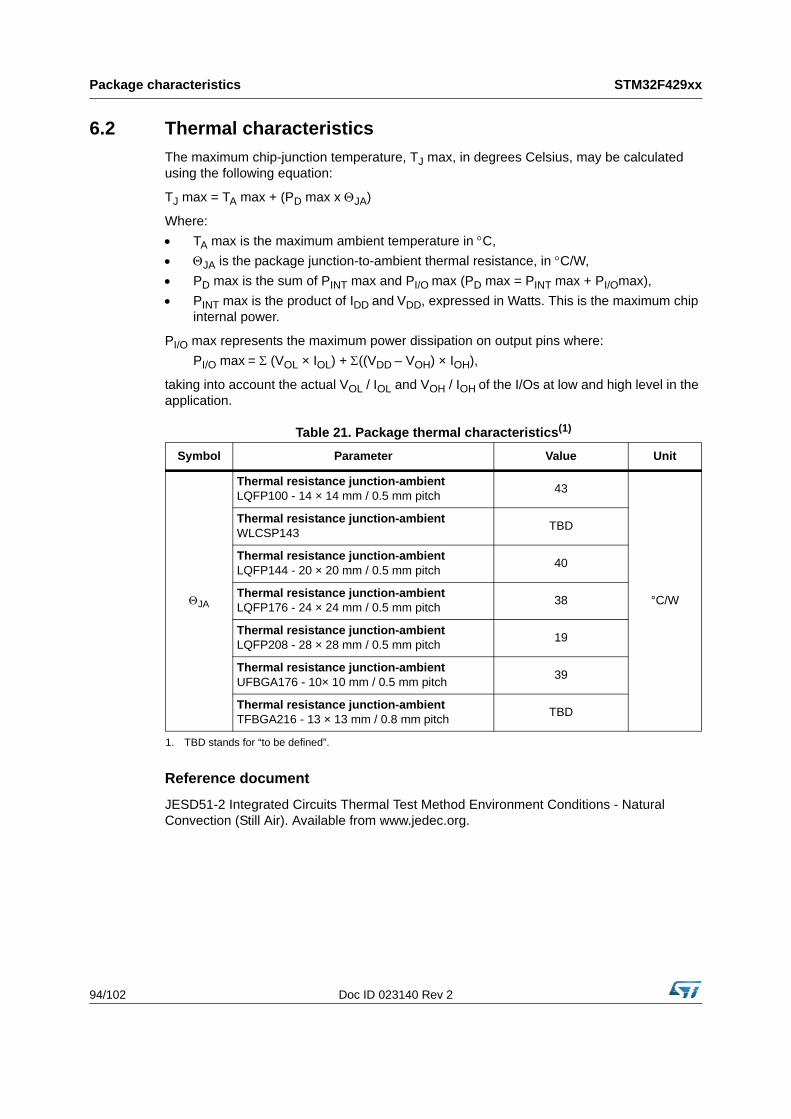
Package characteristics STM32F429xx
94/102 Doc ID 023140 Rev 2
6.2 Thermal characteristicsThe maximum chip-junction temperature, TJ max, in degrees Celsius, may be calculated using the following equation:
TJ max = TA max + (PD max x ΘJA)
Where:• TA max is the maximum ambient temperature in °C,• ΘJA is the package junction-to-ambient thermal resistance, in °C/W,• PD max is the sum of PINT max and PI/O max (PD max = PINT max + PI/Omax),• PINT max is the product of IDD and VDD, expressed in Watts. This is the maximum chip
internal power.
PI/O max represents the maximum power dissipation on output pins where:PI/O max = Σ (VOL × IOL) + Σ((VDD – VOH) × IOH),
taking into account the actual VOL / IOL and VOH / IOH of the I/Os at low and high level in the application.
Reference document
JESD51-2 Integrated Circuits Thermal Test Method Environment Conditions - Natural Convection (Still Air). Available from www.jedec.org.
Table 21. Package thermal characteristics(1)
1. TBD stands for “to be defined”.
Symbol Parameter Value Unit
ΘJA
Thermal resistance junction-ambientLQFP100 - 14 × 14 mm / 0.5 mm pitch 43
°C/W
Thermal resistance junction-ambientWLCSP143 TBD
Thermal resistance junction-ambientLQFP144 - 20 × 20 mm / 0.5 mm pitch 40
Thermal resistance junction-ambientLQFP176 - 24 × 24 mm / 0.5 mm pitch 38
Thermal resistance junction-ambientLQFP208 - 28 × 28 mm / 0.5 mm pitch 19
Thermal resistance junction-ambientUFBGA176 - 10× 10 mm / 0.5 mm pitch 39
Thermal resistance junction-ambientTFBGA216 - 13 × 13 mm / 0.8 mm pitch TBD
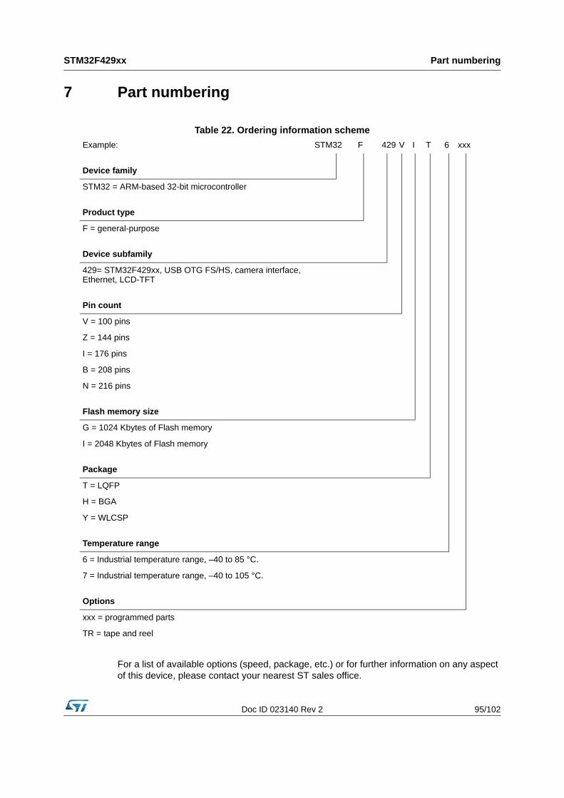
Doc ID 023140 Rev 2 95/102
STM32F429xx Part numbering
7 Part numbering
For a list of available options (speed, package, etc.) or for further information on any aspect of this device, please contact your nearest ST sales office.
Table 22. Ordering information schemeExample: STM32 F 429 V I T 6 xxx
Device family
STM32 = ARM-based 32-bit microcontroller
Product type
F = general-purpose
Device subfamily
429= STM32F429xx, USB OTG FS/HS, camera interface, Ethernet, LCD-TFT
Pin count
V = 100 pins
Z = 144 pins
I = 176 pins
B = 208 pins
N = 216 pins
Flash memory size
G = 1024 Kbytes of Flash memory
I = 2048 Kbytes of Flash memory
Package
T = LQFP
H = BGA
Y = WLCSP
Temperature range
6 = Industrial temperature range, –40 to 85 °C.
7 = Industrial temperature range, –40 to 105 °C.
Options
xxx = programmed parts
TR = tape and reel
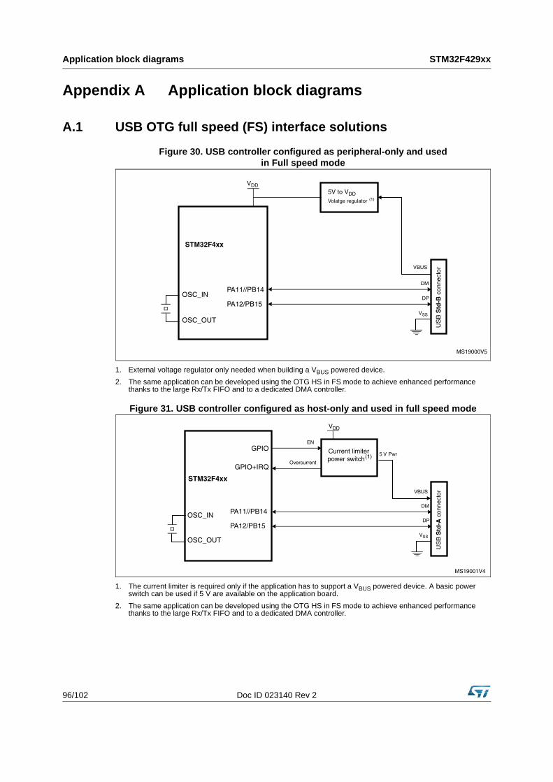
Application block diagrams STM32F429xx
96/102 Doc ID 023140 Rev 2
Appendix A Application block diagrams
A.1 USB OTG full speed (FS) interface solutions
Figure 30. USB controller configured as peripheral-only and used in Full speed mode
1. External voltage regulator only needed when building a VBUS powered device.2. The same application can be developed using the OTG HS in FS mode to achieve enhanced performance
thanks to the large Rx/Tx FIFO and to a dedicated DMA controller.
Figure 31. USB controller configured as host-only and used in full speed mode
1. The current limiter is required only if the application has to support a VBUS powered device. A basic power switch can be used if 5 V are available on the application board.
2. The same application can be developed using the OTG HS in FS mode to achieve enhanced performance thanks to the large Rx/Tx FIFO and to a dedicated DMA controller.
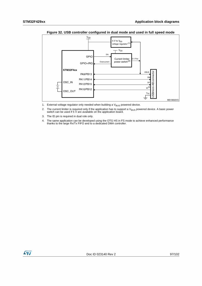
Doc ID 023140 Rev 2 97/102
STM32F429xx Application block diagrams
Figure 32. USB controller configured in dual mode and used in full speed mode
1. External voltage regulator only needed when building a VBUS powered device.2. The current limiter is required only if the application has to support a VBUS powered device. A basic power
switch can be used if 5 V are available on the application board.3. The ID pin is required in dual role only.4. The same application can be developed using the OTG HS in FS mode to achieve enhanced performance
thanks to the large Rx/Tx FIFO and to a dedicated DMA controller.
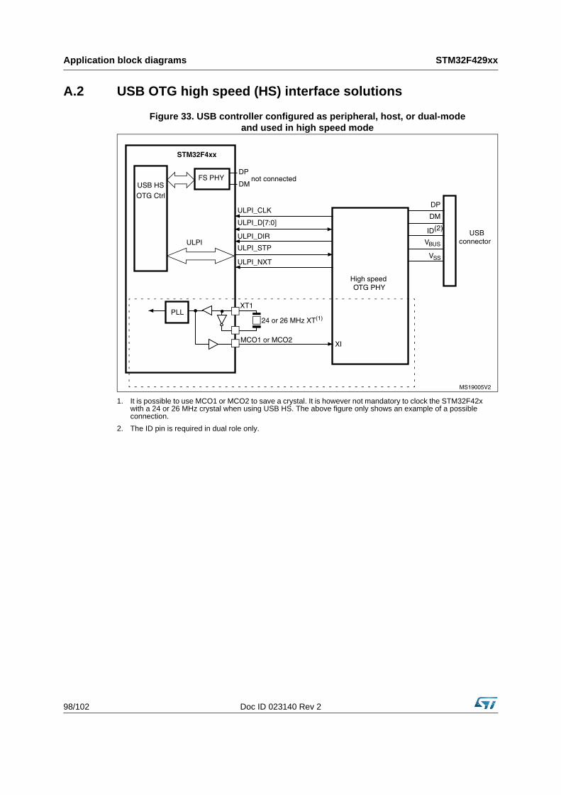
Application block diagrams STM32F429xx
98/102 Doc ID 023140 Rev 2
A.2 USB OTG high speed (HS) interface solutions
Figure 33. USB controller configured as peripheral, host, or dual-modeand used in high speed mode
1. It is possible to use MCO1 or MCO2 to save a crystal. It is however not mandatory to clock the STM32F42x with a 24 or 26 MHz crystal when using USB HS. The above figure only shows an example of a possible connection.
2. The ID pin is required in dual role only.
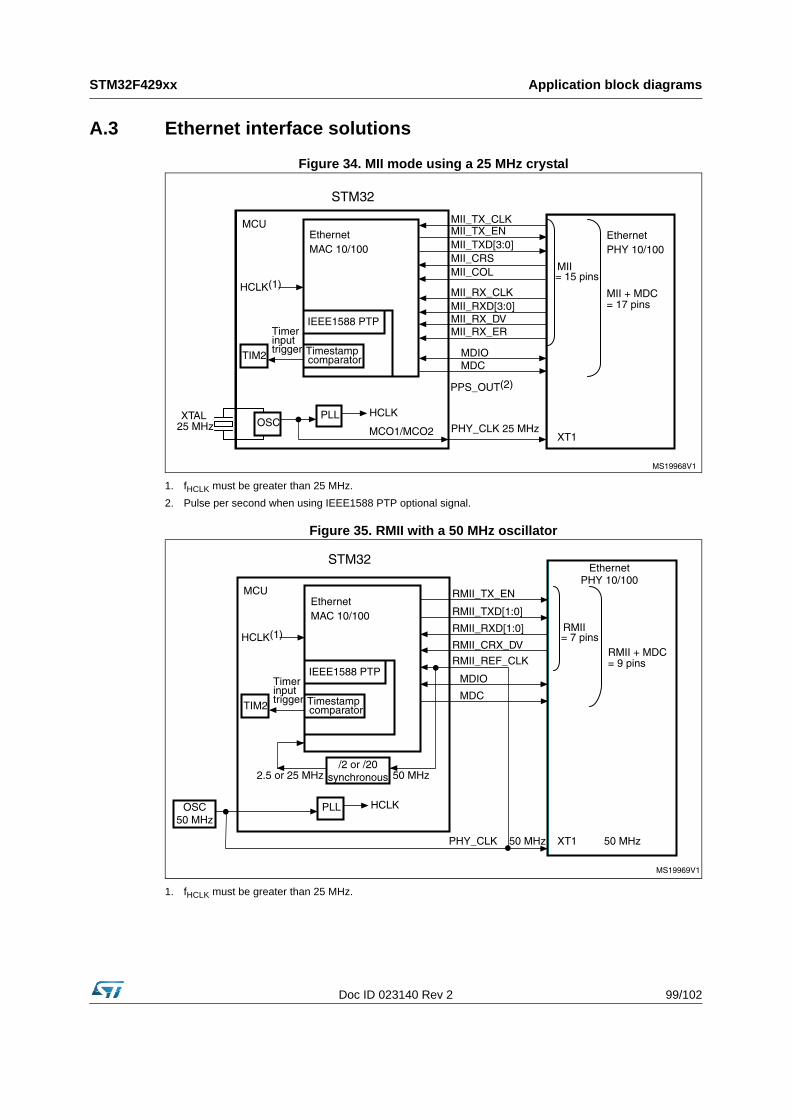
Doc ID 023140 Rev 2 99/102
STM32F429xx Application block diagrams
A.3 Ethernet interface solutions
Figure 34. MII mode using a 25 MHz crystal
1. fHCLK must be greater than 25 MHz. 2. Pulse per second when using IEEE1588 PTP optional signal.
Figure 35. RMII with a 50 MHz oscillator
1. fHCLK must be greater than 25 MHz.
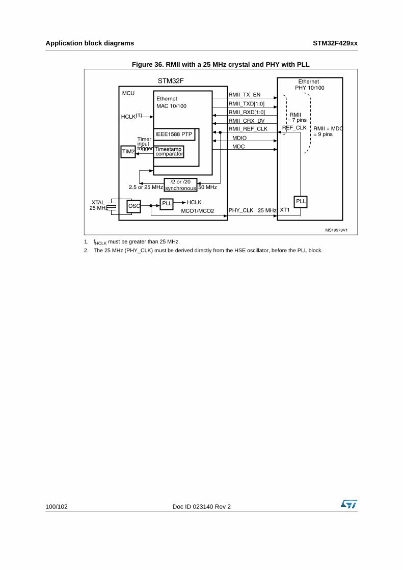
Application block diagrams STM32F429xx
100/102 Doc ID 023140 Rev 2
Figure 36. RMII with a 25 MHz crystal and PHY with PLL
1. fHCLK must be greater than 25 MHz.2. The 25 MHz (PHY_CLK) must be derived directly from the HSE oscillator, before the PLL block.
STM32F429xx Revision history
Doc ID 023140 Rev 2 101/102
8 Revision history
Table 23. Document revision history
Date Revision Changes
13-Feb-2013 1 Initial release.
15-May-2013 2
Removed note 1 on cover page related to WLCSP143.
Replaced Cortex-M4F by Cortex-M4 with FPU. Maximum CPU frequency changed to 180 MHz in Table 2: STM32F429xx features and peripheral counts.Removed mention of WLCSP144 on cover page, and add WLCSP143 in the whole document.Updated Figure 3: Compatible board design between STM32F2xx and STM32F4xx for LQFP176 package.Updated Figure 5: STM32F429xx Multi-AHB matrix.
Updated Figure 14: STM32F42x LQFP176 pinout.
Changed maximum FMC frequency for synchronous accesses to 90 MHz in Section 3.9: Flexible memory controller (FMC).
Changed 1.2 V to V12 and updated DAc output in Section 3.18.2: Regulator OFF.
Updated note 1 in Table 8: USART feature comparison.
Changed LQFP176 pin 36 signal to VDDA in Figure 14: STM32F42x LQFP176 pinout.
Table 10: STM32F429xx pin and ball definitions: added WLCSP143, updated alternate and additional functions.
Updated Table 12: STM32F429xx alternate function mapping.
STM32F429xx
102/102 Doc ID 023140 Rev 2
Please Read Carefully:
Information in this document is provided solely in connection with ST products. STMicroelectronics NV and its subsidiaries (“ST”) reserve theright to make changes, corrections, modifications or improvements, to this document, and the products and services described herein at anytime, without notice.
All ST products are sold pursuant to ST’s terms and conditions of sale.
Purchasers are solely responsible for the choice, selection and use of the ST products and services described herein, and ST assumes noliability whatsoever relating to the choice, selection or use of the ST products and services described herein.
No license, express or implied, by estoppel or otherwise, to any intellectual property rights is granted under this document. If any part of thisdocument refers to any third party products or services it shall not be deemed a license grant by ST for the use of such third party productsor services, or any intellectual property contained therein or considered as a warranty covering the use in any manner whatsoever of suchthird party products or services or any intellectual property contained therein.
UNLESS OTHERWISE SET FORTH IN ST’S TERMS AND CONDITIONS OF SALE ST DISCLAIMS ANY EXPRESS OR IMPLIEDWARRANTY WITH RESPECT TO THE USE AND/OR SALE OF ST PRODUCTS INCLUDING WITHOUT LIMITATION IMPLIEDWARRANTIES OF MERCHANTABILITY, FITNESS FOR A PARTICULAR PURPOSE (AND THEIR EQUIVALENTS UNDER THE LAWSOF ANY JURISDICTION), OR INFRINGEMENT OF ANY PATENT, COPYRIGHT OR OTHER INTELLECTUAL PROPERTY RIGHT.
ST PRODUCTS ARE NOT AUTHORIZED FOR USE IN WEAPONS. NOR ARE ST PRODUCTS DESIGNED OR AUTHORIZED FOR USEIN: (A) SAFETY CRITICAL APPLICATIONS SUCH AS LIFE SUPPORTING, ACTIVE IMPLANTED DEVICES OR SYSTEMS WITHPRODUCT FUNCTIONAL SAFETY REQUIREMENTS; (B) AERONAUTIC APPLICATIONS; (C) AUTOMOTIVE APPLICATIONS ORENVIRONMENTS, AND/OR (D) AEROSPACE APPLICATIONS OR ENVIRONMENTS. WHERE ST PRODUCTS ARE NOT DESIGNEDFOR SUCH USE, THE PURCHASER SHALL USE PRODUCTS AT PURCHASER’S SOLE RISK, EVEN IF ST HAS BEEN INFORMED INWRITING OF SUCH USAGE, UNLESS A PRODUCT IS EXPRESSLY DESIGNATED BY ST AS BEING INTENDED FOR “AUTOMOTIVE,AUTOMOTIVE SAFETY OR MEDICAL” INDUSTRY DOMAINS ACCORDING TO ST PRODUCT DESIGN SPECIFICATIONS.PRODUCTS FORMALLY ESCC, QML OR JAN QUALIFIED ARE DEEMED SUITABLE FOR USE IN AEROSPACE BY THECORRESPONDING GOVERNMENTAL AGENCY.
Resale of ST products with provisions different from the statements and/or technical features set forth in this document shall immediately voidany warranty granted by ST for the ST product or service described herein and shall not create or extend in any manner whatsoever, anyliability of ST.
ST and the ST logo are trademarks or registered trademarks of ST in various countries.Information in this document supersedes and replaces all information previously supplied.
The ST logo is a registered trademark of STMicroelectronics. All other names are the property of their respective owners.
© 2013 STMicroelectronics - All rights reserved
STMicroelectronics group of companies
Australia - Belgium - Brazil - Canada - China - Czech Republic - Finland - France - Germany - Hong Kong - India - Israel - Italy - Japan - Malaysia - Malta - Morocco - Philippines - Singapore - Spain - Sweden - Switzerland - United Kingdom - United States of America
www.st.com