anurag dwivedi. verilog- hardware description language modules combinational circuits assign...
TRANSCRIPT

FPGA Design Challenge :Techkriti’14
Digital Design using Verilog – Part 2
Anurag Dwivedi
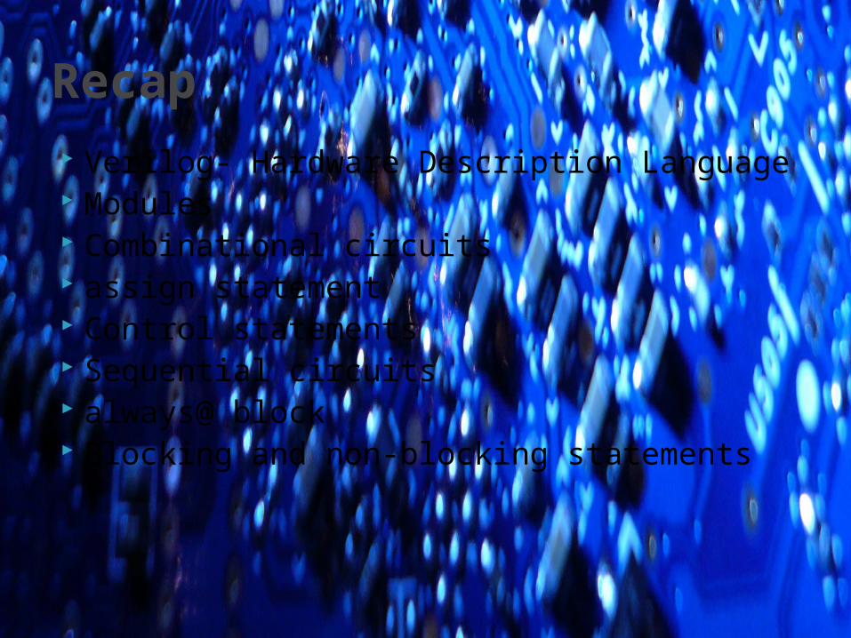
Verilog- Hardware Description Language Modules Combinational circuits assign statement Control statements Sequential circuits always@ block Blocking and non-blocking statements
Recap

Time to construct larger modules from smaller modules.
Various modules are interconnected to make a larger circuit (or module).
Each sub-module has a separate Verilog file. A sub-module may have another sub-module in its circuit. One needs to indicate the top level module before
synthesis.
Modular Circuits

Sub-module 1 module Sub1 (input wire [7:0] a1, output wire [7:0] b1);
Sub-module 2
module Sub2 (input wire [7:0] a2, output wire[7:0] b2);
Top Module Module Top (input wire [7:0] a, output wire[7:0] b);
Example
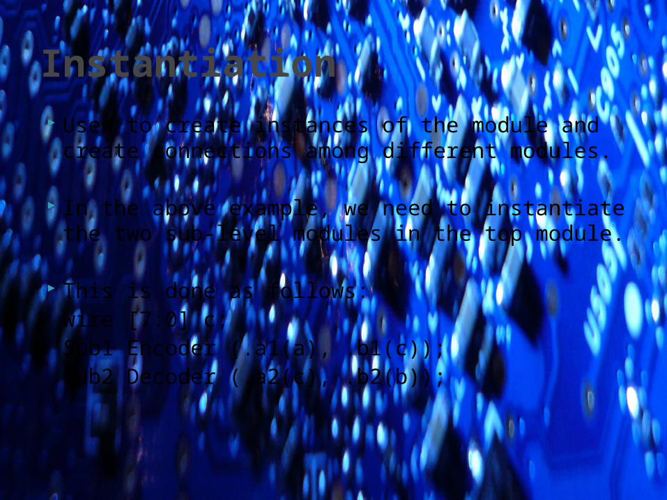
Used to create instances of the module and create connections among different modules.
In the above example, we need to instantiate the two sub-level modules in the top module.
This is done as follows: wire [7:0] c; Sub1 Encoder (.a1(a), .b1(c)); Sub2 Decoder (.a2(c), .b2(b));
Instantiation
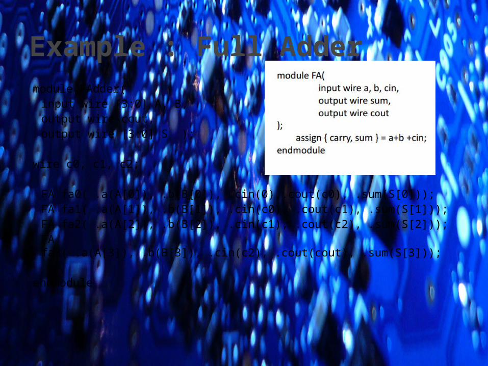
module FAdder( input wire [3:0] A, B, output wire cout, output wire [3:0] S );
wire c0, c1, c2;
FA fa0( .a(A[0]), .b(B[0]), .cin(0),.cout(c0), .sum(S[0])); FA fa1( .a(A[1]), .b(B[1]), .cin(c0), .cout(c1), .sum(S[1])); FA fa2( .a(A[2]), .b(B[2]), .cin(c1), .cout(c2), .sum(S[2])); FA fa3( .a(A[3]), .b(B[3]), .cin(c2), .cout(cout), .sum(S[3]));
endmodule
Example : Full Adder

All output ports of instantiated sub-module should be of wire data-type.
Note in previous example, c0,c1,c2 and S are wires.
Inputs may be reg or wire.
Suppose in above, [3:0] S was of reg type. ◦ Declare a dummy wire variable [3:0] add◦ Pass add[0], add[1] … to the instantiations ◦ Finally put:
always@(*) S <= add;
Points to note

A generalized type of module. Can be instantiated to any value of
parameter. Parameterization is a good practice for
reusable modules Useful in large circuits.
Parameterized Modules
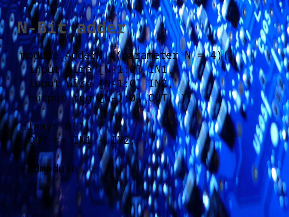
N-Bit adder
module AdderN #(parameter N = 4)( input wire [N-1:0] IN1, input wire [N-1:0] IN2, output reg [N-1:0] OUT );
always @(*)
OUT <= IN1 + IN2;
endmodule
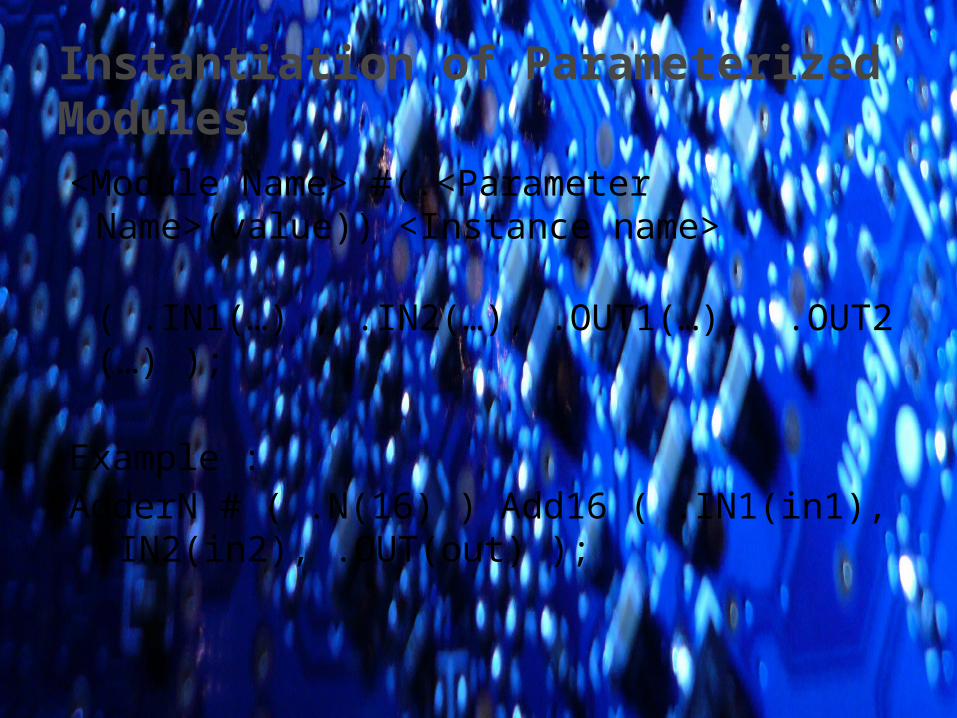
<Module Name> #(.<Parameter Name>(value)) <Instance name>
( .IN1(…) , .IN2(…), .OUT1(…), .OUT2(…) );
Example :AdderN # ( .N(16) ) Add16
( .IN1(in1), .IN2(in2), .OUT(out) );
Instantiation of Parameterized Modules
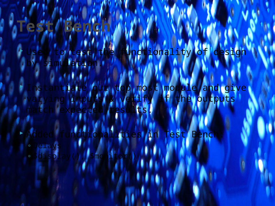
Used to test the functionality of design by simulation.
Instantiate our top most module and give varying inputs & verify if the outputs match expected results.
Added functionalities in Test Bench: ◦ Delays ◦ $display(), $monitor()
Test Bench

Not synthesized Can be used to model delays in actual circuit during simulation
Used mostly in Test Benches to provide inputs at particular instants.
Syntax: #<time steps> ◦ #10 q = x + y; // inter assignment delay◦ q = #10 x + y; // intra assignment delay ◦ Most common: always
#5 clk = ~clk;
Delays
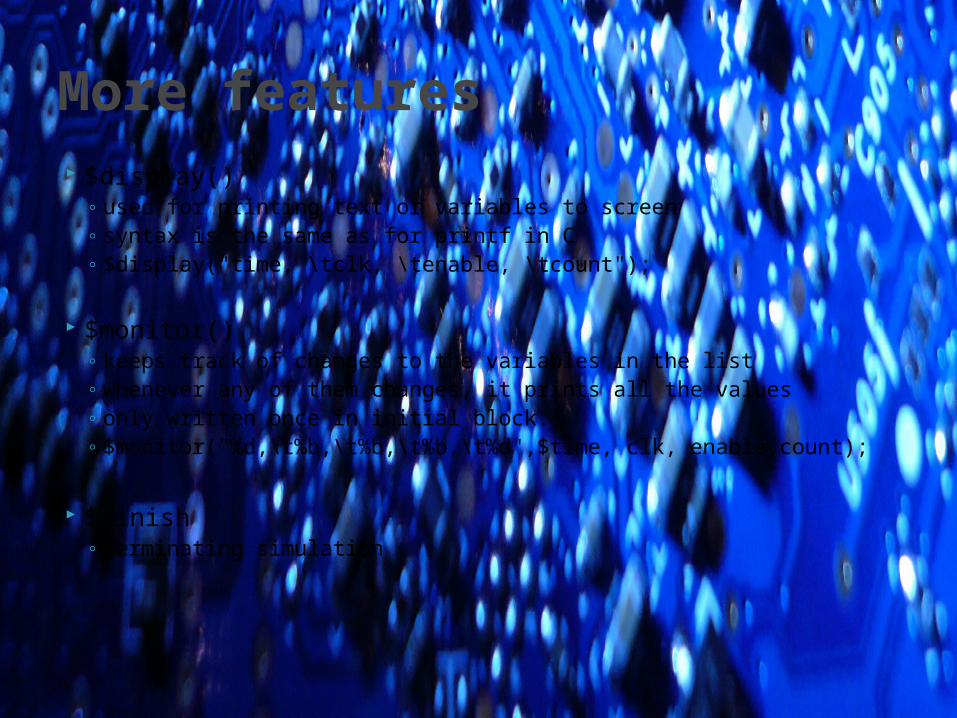
$display() ◦ used for printing text or variables to screen ◦ syntax is the same as for printf in C ◦ $display("time, \tclk, \tenable, \tcount");
$monitor()
◦ keeps track of changes to the variables in the list◦ whenever any of them changes, it prints all the values ◦ only written once in initial block. ◦ $monitor("%d,\t%b,\t%b,\t%b,\t%d",$time, clk, enable,count);
$finish ◦ Terminating simulation
More features

module counter_tb; reg clk, reset, enable; wire [3:0] count;
counter C0( .clk (clk), .reset (reset), .enable (enable), .count (count) ); initial begin clk = 0; reset = 0; enable = 0; end always
#5 clk = !clk; initial begin $display("time,\tclk,\tenable,\tcount"); $monitor("%d,\t%b,\t%b,\t%d",$time, clk,enable,count); end initial #100 $finish;
endmodule
Test Bench Counter
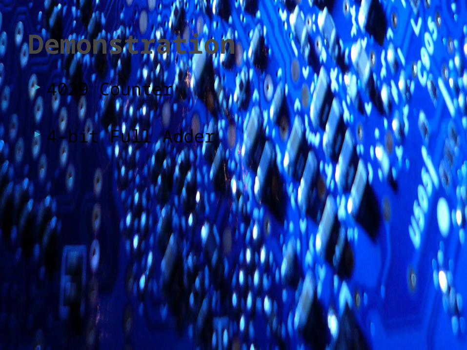
4029 Counter
4-bit Full Adder
Demonstration

Problem Statement :The challenge in FPGA is to design and efficiently implement the Hilbert transformation of any given function.
It maps a time domain function to another time domain function by a convolution of the input signal with the function H(t) whose representation in frequency domain is:
Frequency domain representation of Hilbert Transform
FPGA Design Challenge Techkriti’14
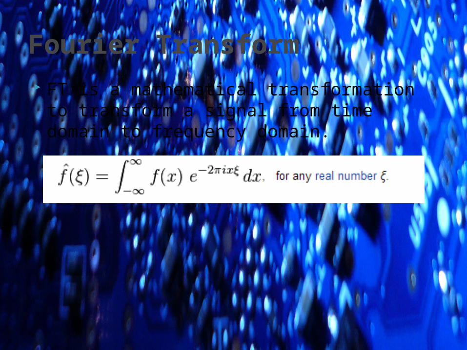
FT is a mathematical transformation to transform a signal from time domain to frequency domain.
Fourier Transform
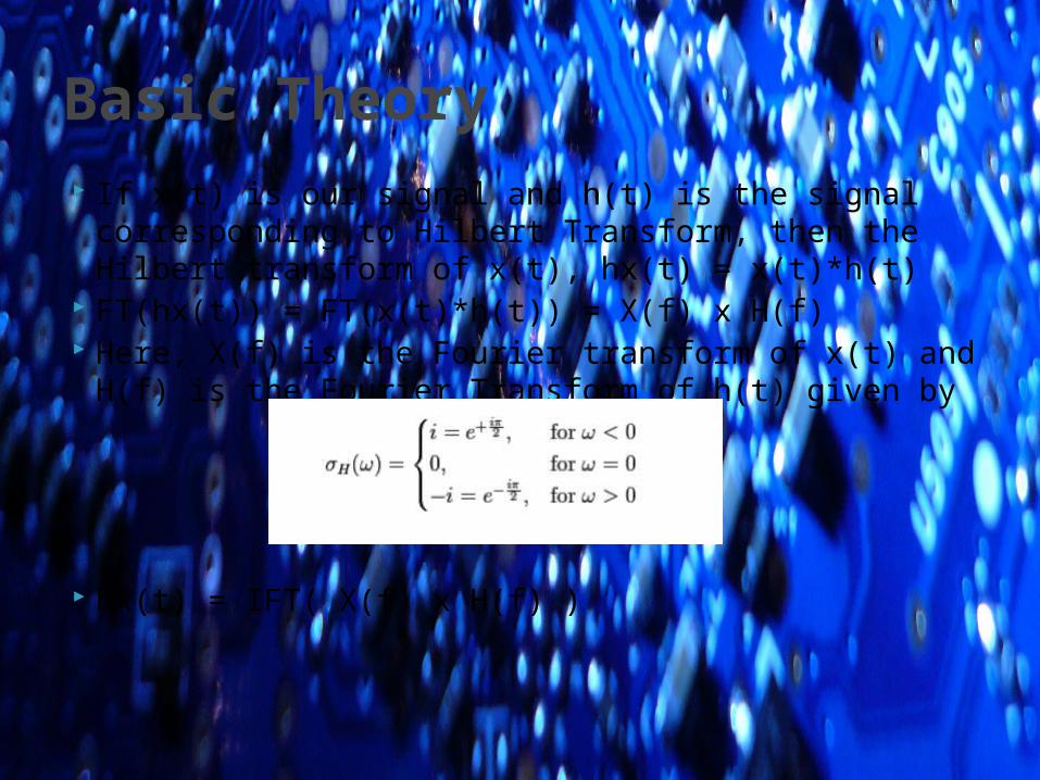
If x(t) is our signal and h(t) is the signal corresponding to Hilbert Transform, then the Hilbert transform of x(t), hx(t) = x(t)*h(t)
FT(hx(t)) = FT(x(t)*h(t)) = X(f) x H(f) Here, X(f) is the Fourier transform of x(t) and H(f) is
the Fourier Transform of h(t) given by
hx(t) = IFT( X(f) x H(f) )
Basic Theory

Find Fourier Transform of the function. Multiply the FT by H(f) Apply inverse Fourier Transform of the
function obtained.
Basic Theory
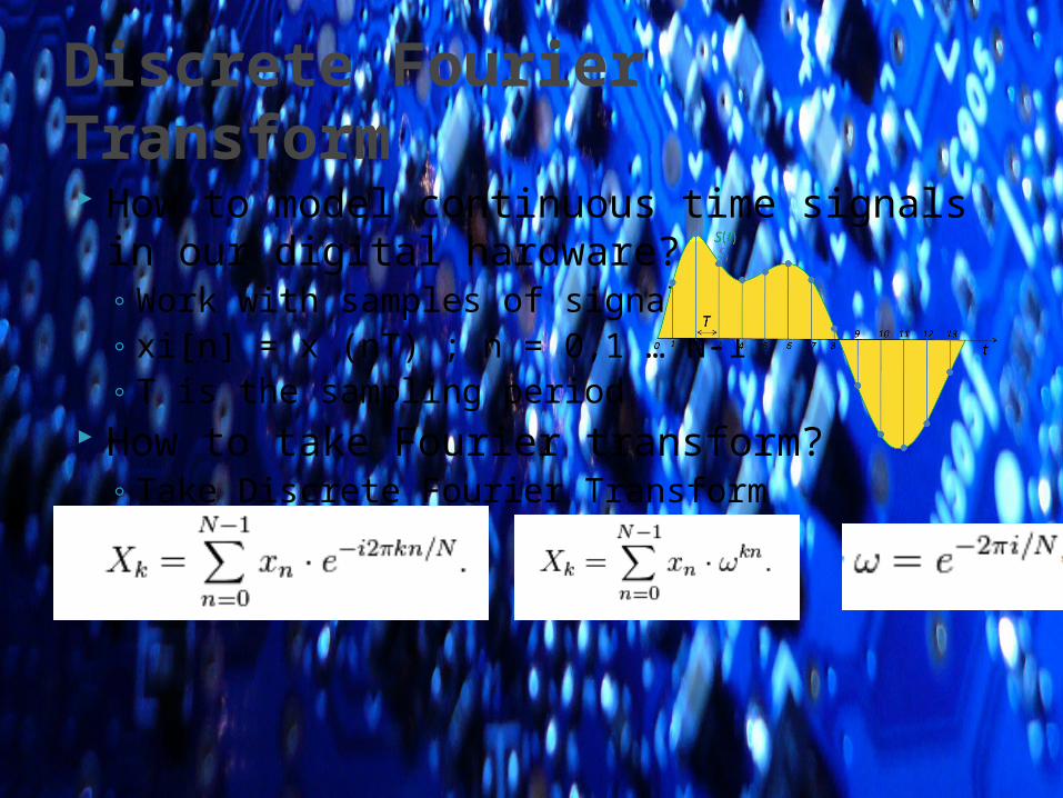
How to model continuous time signals in our digital hardware?◦ Work with samples of signal◦ xi[n] = x (nT) ; n = 0,1 … N-1◦ T is the sampling period
How to take Fourier transform?◦ Take Discrete Fourier Transform
Discrete Fourier Transform
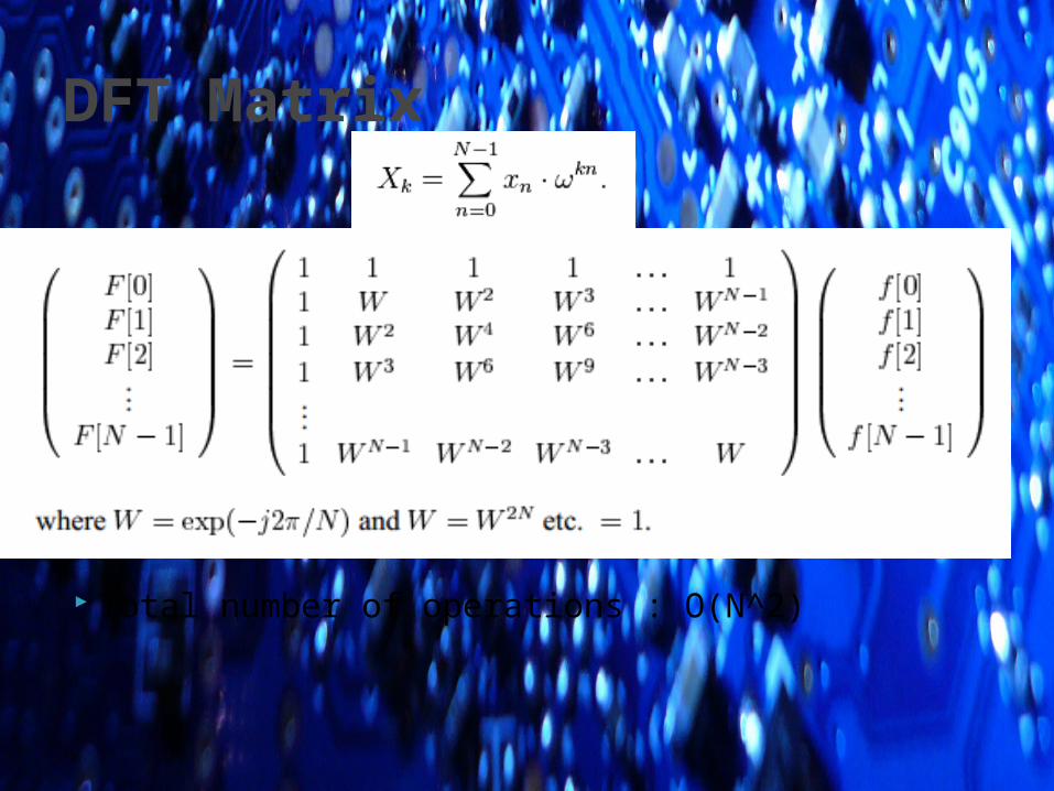
Total number of operations : O(N^2)
DFT Matrix
Computation of DFT involves a lot of redundant operations
Time complexity can be reduced drastically by using this information
A class of algorithms known as Fast Fourier Transform (FFT) is developed for the same
Fast Fourier Transform

When N is a factor of 2 We have
Writing the odd and even numbered terms separately
Taking out the common factor
Cooley–Tukey algorithm : Radix 2 case

Because of Periodicity of DFT we have
Finally,
Cooley–Tukey algorithm : Radix 2 case

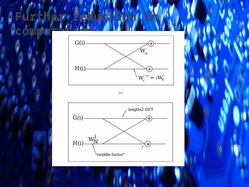
Further reduction in computation

Complete Structure
O(N log(N))

To implement Hilbert transform in Verilog◦ Find FFT of sequence◦ Multiply it by –j sgn(k) ◦ Take IFFT of the resulting sequence
Basic Theory

The approach mentioned above is one of the many possible solutions to the problem statement.
You should search more and look for better solutions.
Note

Area (#LUTs, #FFs, #BRAMs, #DSP Elements etc.)
Latency (No. of cycles Reqd). Need for external memory (eg. DRAM
Controller – DDR/DDR2 and size of memory required).
Maximum frequency achieved. Power consumption as reported by ISE tool. Extra Feature : Implementation of a feature
where Hilbert transform is being used
Judging criteria