anl firmware for lbl digitizer - university of north...
TRANSCRIPT

Digital Gammasphere Firmware User’s Manual
Firmware for the LBL Digitizer module Combined leading‐edge/CFD Build
‐‐ ‐‐
April 19th, 2016 Version 1.9
Originator: J. Anderson
Document #TBA

Table of Contents TABLE OF FIGURES .................................................................................................................................................... 3
INTRODUCTION ....................................................................................................................................................... 4
HARDWARE INTERFACE TO DETECTORS ...................................................................................................... 4
GENERAL DESIGN OF THE FIRMWARE ........................................................................................................... 5
CHANNEL ARCHITECTURE IN THE LEADING-EDGE DISCRIMINATOR MODE .................................................................. 6 DIFFERENCE IN OPERATION OF THE CONSTANT-FRACTION MODE .............................................................................. 7 RELATIONSHIP OF DELAY BLOCKS TO THE INPUT SIGNAL ......................................................................................... 8
INPUT HANDLING SECTION ................................................................................................................................. 9
ADC RECODE BLOCK .............................................................................................................................................. 10 INTRA-DETECTOR DELAY P1 ................................................................................................................................... 10 INTER-DETECTOR DELAY P2 ................................................................................................................................... 10 COARSE PRE-DISCRIMINATOR .................................................................................................................................. 10
ENERGY SUM AND DISCRIMINATOR OPERATION ..................................................................................... 11
ENERGY SUMMATION LOGIC ................................................................................................................................... 12 Comparison of delays and sums versus the standard trapezoidal filter ............................................................. 12
DISCRIMINATOR FILTER ........................................................................................................................................... 13 LEADING-EDGE DISCRIMINATOR OPERATION ........................................................................................................... 14 LEADING-EDGE DISCRIMINATOR RETRIGGER HOLD-OFF .......................................................................................... 15 CONSTANT-FRACTION DISCRIMINATOR ................................................................................................................... 17 LEADING-EDGE HOLD-OFF INTERACTION WITH CFD OPERATION ............................................................................. 19
PEAK DETECTION AND PILEUP REJECTION ................................................................................................ 20
PEAK DETECTOR...................................................................................................................................................... 20 PILEUP DETECTION LOGIC ....................................................................................................................................... 20 RELATIONSHIP BETWEEN DISCRIMINATOR HOLD-OFF AND PILEUP TIMES ................................................................. 21 TRIGGER DELAY BUFFER ........................................................................................................................................ 22
Effects of delayed discriminator bit formation ................................................................................................... 22 BASELINE MEASUREMENT ....................................................................................................................................... 22
EVENT COLLECTION AND READOUT ............................................................................................................. 25
EVENT QUEUING ..................................................................................................................................................... 25 USE OF THE PENDING EVENT QUEUE (INTERNAL VS. EXTERNAL TRIGGERING) ........................................................ 26 WAVEFORM READOUT GENERALITIES .................................................................................................................... 26 DATA COLLECTION ACROSS THE DIGITIZER AND READOUT OVER VME ................................................................. 26
Waveform Decimation ........................................................................................................................................ 27 PILEUP AND EVENT READOUT ................................................................................................................................. 28 READOUT INTERFERENCE ........................................................................................................................................ 28
Readout Interference when Decimation is in use ............................................................................................... 29 PILEUP EXTENSION AND READOUT MODES ............................................................................................................. 29
Readout Modes when Pileup Extension is Disabled .......................................................................................... 30 Readout operation when Pileup Extension is Enabled ....................................................................................... 31
DATA READOUT FORMAT ........................................................................................................................................ 33 Data Header – leading-edge discriminator mode .............................................................................................. 33 Data Header – CFD mode ................................................................................................................................. 35
WAVEFORM DATA FORMAT DETAILS ...................................................................................................................... 36
INTERFACE TO THE EXTERNAL TRIGGER ................................................................................................... 37
TIMESTAMP SYNCHRONIZATION .............................................................................................................................. 37 EVENT VETO ........................................................................................................................................................... 37

TRIGGER DECISION LATENCY .................................................................................................................................. 38 Details of the trigger window calculation .......................................................................................................... 38
OTHER COMMANDS FROM THE TRIGGER ................................................................................................................. 40 INFORMATION SENT TO THE TRIGGER SYSTEM BY THE DIGITIZER .......................................................................... 40 DATA FLOW CONTROL (THROTTLE) ........................................................................................................................ 40
MASTER AND SLAVE DIGITIZERS .................................................................................................................... 42
DETAILED DESCRIPTION OF EXTERNAL DISCRIMINATOR MODES ............................................................................ 43 TYPICAL MODES OF SLAVE DIGITIZER OPERATION .................................................................................................. 44
Gammasphere “Independent” Mode ................................................................................................................. 45 Gammasphere “Clean”, “Dirty” and “Module” Modes with Slave Digitizers................................................. 45 “Pseudo-GRETINA” Mode ................................................................................................................................ 47
TECHNICAL DETAILS OF CHANNEL PIPELINE OPERATION .................................................................. 48
MEMORY STRUCTURES WITHIN XILINX FPGAS ...................................................................................................... 48 DELAY STRUCTURES WITHIN THE CHANNEL LOGIC ................................................................................................ 49
Chain Validity Logic (system initialization) ....................................................................................................... 49 Waveform Readout ............................................................................................................................................. 50 CFD timing control ............................................................................................................................................ 50 Pileup timing ...................................................................................................................................................... 50
DIAGNOSTIC CAPABILITIES USING THE ON-BOARD DAC .......................................................................................... 50 ACCURACY AND POLE-ZERO CONSIDERATIONS ....................................................................................................... 51 TIME INTERPOLATION USING THE CFD SAMPLE VALUES ......................................................................................... 53
Table of Figures FIGURE 1 – CHANNEL ARCHITECTURE IN THE THRESHOLD DISCRIMINATOR MODE. ........................................................................... 7 FIGURE 2 ‐ CHANNEL ARCHITECTURE IN THE CONSTANT‐FRACTION DISCRIMINATOR MODE. ................................................................ 8 FIGURE 3 ‐ DELAY BUFFER POSITIONS AT MOMENT THE LEADING‐EDGE DISCRIMINATOR FIRES, AS SHOWN IN GAMMAWARE .................... 8 FIGURE 4 ‐ INPUT SIGNAL HANDLING PORTION OF CHANNEL LOGIC ................................................................................................ 9 FIGURE 5A ‐ DISCRIMINATOR AND ENERGY SUMMATION PORTION OF CHANNEL LOGIC (LEADING‐EDGE MODE). ................................. 11 FIGURE 6 ‐ PRE‐ AND POST‐RISE ACCUMULATOR LOGIC ............................................................................................................ 12 FIGURE 7 ‐ ESTIMATED FREQUENCY RESPONSE PLOT OF DIGITAL LEADING‐EDGE DISCRIMINATOR FILTER. ............................................ 14 FIGURE 8 ‐ TYPICAL INPUT SIGNAL AND DERIVED SIGNALS FOR LEADING EDGE DISCRIMINATOR .......................................................... 15 FIGURE 9A ‐ HOLD‐OFF MANUALLY SET.................................................................................................................................. 16 FIGURE 10 – DISCRIMINATOR AND ENERGY SUMMATION PORTION OF CHANNEL LOGIC (CFD MODE). .............................................. 18 FIGURE 11 ‐ SCREEN CAPTURE FROM GAMMAWARE SHOWING POSITIONS OF BUFFERS IN CFD MODE .............................................. 19 FIGURE 12 ‐ SIMULATION SHOWING OPERATION OF PILEUP COUNTER. ........................................................................................ 21 FIGURE 13 ‐ CHANNEL READOUT STRUCTURE ......................................................................................................................... 25 FIGURE 14 ‐ EXAMPLE WAVEFORM FOR DESCRIBING PILEUP READOUT MODES .............................................................................. 29 FIGURE 15 ‐ VISUAL REPRESENTATION OF THE READOUT MODES WITH PILEUP EXTENSION DISABLED .............................................. 31 FIGURE 16 ‐ VISUAL REPRESENTATION OF THE READOUT MODES WITH PILEUP EXTENSION ENABLED .............................................. 33 FIGURE 17 ‐ TRIGGER WINDOWS WITHIN THE DIGITIZER ........................................................................................................... 39 FIGURE 18 ‐ CONNECTIONS BETWEEN MASTER AND SLAVE DIGITIZERS. ....................................................................................... 43 FIGURE 19 ‐ TIMING MODEL OF THE CHANNEL LOGIC ............................................................................................................... 49 FIGURE 20 ‐ CORRECTION OF CURRENT EVENT FROM DATA PASSED FORWARD FROM THE PREVIOUS EVENT. ........................................ 52
Introduction The experiments at the ATLAS beamline at Argonne National Laboratory (Gammasphere, FMA, DSSD) have re‐instrumented their detectors with digital data acquisition systems based upon the use of the hardware developed for the GRETINA experiment. Although the hardware is the same the differing architectures of the experiments and different detector structures necessitate new firmware in both the digitizer and trigger modules. A generic firmware design from which specific variants for each of the ATLAS experiments can be derived is described herein. It is our hope that this firmware development, where all channels are independent and equal, may be utilized in other experiments as well. Both new digital data acquisition systems of Digital Gammasphere (DGS) and Digital FMA (DFMA) use this firmware, plus a couple of small Clover detectors. The HELIOS (Helical Orbit Spectrometer) is, as of 2015, installing a new DAQ also based upon this firmware. The digitizer module design and the original GRETINA firmware developed for it are products of Lawrence Berkeley National Laboratory (LBNL). The trigger module and its firmware are products of Argonne National Laboratory (ANL). We at Argonne thank our LBNL collaborators for sharing the source code and schematics of the digitizer module, both of which were invaluable references in this totally new firmware development. Data from the ADCs of the digitizer is signed 14‐bit values that arrive at 100MHz (10ns period). Each digitizer module implements ten channels that implement independent input and energy integration blocks. The purpose of the input and energy integration firmware block, implemented as a pipeline, is to receive the data, internally trigger on the leading edges of signals and calculate the energy of the input signal. Following each energy integrator is a pending event queue and event acceptance logic block that places accepted events into channel‐specific FIFO buffers. At the back end, a channel readout machine collects all data from the channels and stuffs accepted events into a large external readout FIFO, accessible over the VME backplane. Two versions of firmware have been developed, a Master build and a Slave build. These operate identically in virtually all ways save that the Master build directly interfaces to the trigger system and the Slave build receives its control from the trigger through the Master. The bulk of this document describes the Master design. A chapter at the end details the differences in the Slave.
Hardware Interface to Detectors The signals from detectors are processed through external analog interface modules before connection to the digitizer. As an example, in the case of Digital Gammasphere ‘pickoff cards’ differentiate the single‐ended input signal to remove the long ramp and reset associated with the transistor‐reset preamplifiers. These cards then drive the resultant signal differentially into the digitizer with a potentiometer‐controlled DC offset. Thus the signal applied to the digitizers is unipolar with the dominant time constant defined by the differentiator’s RC timing. The time constant of the pickoff card is 50us; sufficiently long that pileup is inevitable when

detector rates exceed approximately 10kHz. The firmware detects piled‐up pulses and identifies them in a way that the analysis software can determine energies of the individual pulses within the piled‐up train.
General Design of the Firmware The ANL version of digitizer firmware implements an independent data acquisition pipeline in each of ten channels. Pileup detection & rejection is performed locally within the digitizer. Selective readout of events is achieved using an external trigger system. Waveform readout of all events is possible, with up to 2048 ADC samples per channel per event, although this will limit the event rate as the backplane reaches its bandwidth limit. Increased event rates are obtained by limiting the amount of waveform data read out per event. Each channel pipeline consists of a series of memory buffers used for delay. Discriminator logic recognizes edges within the input signal and causes data values to be sampled. The discriminator logic may be configured as either a leading‐edge (slope) or a constant‐fraction architecture, sensitive to either positive‐only, negative‐only or both edges. The discriminator implements a programmable hold‐off time to provide customized performance matching the shaping time of the input signal. At the moment the discriminator fires specific ADC samples plus specific sums and baseline information is sampled, so that discriminator firing rates over 1MHz can be supported. No information reduction occurs in pileup conditions due to the fast discriminator recovery time.
All sampled values and sums are formatted into an event header that is followed by a programmable number of waveform samples. Information stored within the header includes the timestamp of the event, the timestamp of the last time the discriminator of that channel fired, the peak ADC value in the event, the timestamp of the peak, energy information, the baseline at the time of the event and a number of additional ADC samples from the event that provide useful diagnostics. The waveform data contains the raw ADC samples of the event, plus some flag bits that indicate on which sample the discriminator and the peak finder fired.
Energy measurement is performed in a double‐correlated method timed relative to the
moment the discriminator fires. Two identically sized, but programmable, delay buffers have accumulators continuously calculating the sum of all the ADC samples within them. When the discriminator fires these two sums are saved and reported in the header. These two sums may then be used by software to calculate the energy (amplitude) of the input signal, with all necessary baseline and pole‐zero correction information obtained from the other information in the header. This method is arithmetically identical to the traditional “trapezoid” method but is optimized for high rate operation. Events captured by the discriminator may optionally be rejected if pileup occurs. If piled‐up events are allowed the piling‐on events may be read out in a variety of ways including extended and offset waveforms or just additional headers. The reverse logic is also supported, in which only piled‐up events are available for readout. The firmware interfaces with the GRETINA trigger module (programmed with the Digital Gammasphere version of firmware) to

provide event selection based upon trigger conditions such as multiplicity. Mapping options in the DGS version of the trigger allow the user to arbitrarily map digitizer channels throughout the system into two “virtual planes” with multiplicity of each virtual plane calculated separately and simultaneously. Triggers using these channel mapping modes, designed specifically for dual‐sided silicon strip and Clover detectors, have been implemented. Signal edges marked by discriminator firings become accepted hits after passing through pileup rejection logic. The discriminator may fire on rising or falling edges. When running in “internal” mode (no triggers from trigger system) these accepted hits immediately become accepted events that are later read out. When the trigger system is used, accepted hits wait in a queue for a limited time. Events in this queue only become accepted events if selected by the trigger. Events that are accepted are read out; events not marked as accepted events fall off the end of the pipeline and are discarded. The trigger system and the digitizer firmware work in concert to implement a dirty event veto mechanism for shielded detectors that removes the top accepted hit in the queue from the pair of channels associated with the Ge core and the shield if the event is “dirty”, so that the “dirty” event is no longer available to be chosen as an accepted event. Events selected for readout are copied from the firmware into a board‐wide FIFO buffer. A waveform compression mechanism referred to as “decimation” allows the user to average together a programmable binary‐weighted number of samples so that a larger time span may be covered by the limited number of words of waveform data that may be read out per event. The compression may be run in an “on‐off” mode that compresses only the waveform segments between edges, reading out the edges of waveforms at full speed. The firmware implements a flow control mechanism (“throttle”) that signals the trigger system if the on‐board FIFO becomes too full. When asserted the throttle vetoes all trigger decisions so that the readout may catch up with the events already stored. Counters within the digitizer monitor the rates of discriminator firings, accepted hits, accepted events and dropped events, allowing easy monitoring of overall operation. To accommodate detectors with transistor‐reset preamps, a “reset kill” timer may be enabled that temporarily vetoes the discriminator when large pulses of polarity opposite to that desired occur.
Channel architecture in the leading-edge discriminator mode An overall picture of the channel pipeline in the simpler threshold, or leading‐edge,
discriminator mode is shown in Figure 1. Colored blocks indicate delay elements; white blocks are logic. Gray blocks are fixed delays, while the others are programmable. Other colors indicate function:
Yellow blocks are delays used for system timing alignment.
Green blocks are energy summation buffers.
Orange blocks are used to span any excess rise time at the beginning or end of the rise to properly align the green blocks for best energy measurement.
Red blocks are associated with discriminator operation.

Figure 1 – Channel architecture in the leading‐edge discriminator mode.
In this architecture the threshold, or leading‐edge, discriminator is located in the middle of the delay chain. Please note that this document eschews the use of the “LED” abbreviation for Leading‐Edge Discriminator to avoid confusion with “LED” for Light‐Emitting Diode. The abbreviation “LED”, if found, will only refer to Light‐Emitting Diode. The mode of the discriminator will always be described using the full words “leading‐edge” or “constant‐fraction”.
The leading‐edge discriminator is the essential element that causes all other logic blocks to capture data. At the moment the leading‐edge discriminator logic is satisfied, simultaneous sampling of both accumulator sums occurs, and both the peak and pileup logic blocks are enabled. Since there is no waiting after the discriminator firing to form sums, the discriminator can re‐arm within 10s of nanoseconds, allowing for very fast event rates. A user‐programmable “retrigger hold‐off” parameter ensures that the threshold discriminator fires only once per leading edge. To reduce the effects of noise a digital low‐pass filter is placed between the raw ADC data and the discriminator logic. As this digital filter requires multiple clocks to process a fixed compensatory delay is added to the raw sample pipeline to maintain alignment of functions.
Difference in operation of the Constant-Fraction mode The channel design is slightly changed in when constant‐fraction mode is enabled, as shown in Figure 2. The user may select between leading‐edge and constant‐fraction mode by setting a bit in a control register. The default mode of operation is leading‐edge. The threshold discriminator logic moves forward one delay block, and the center delay “d” is now monitored by the constant‐fraction discriminator (CFD). The leading‐edge discriminator is used to gate the operation of the CFD, to avoid false firings. The leading‐edge discriminator fires as the leading edge of the waveform passes through the “k” buffer. The CFD logic starts calculating when the leading‐edge discriminator fires, and the CFD itself fires when the CFD equation at the selection fraction is satisfied.
ADCRECODE
CoarsePre-Disc
Post-risedelay
RiseRemainder
Disc.Delay
PipelineCompensate
WaveformOffset
Pre-riseDelay
TriggerDelay14 14 14 14 14 14 14 1414
ADCDATA
TriggerDelay
160ns delay
10nsdelay
0-10.23usdelay
0-1.27usdelay
0-1.27usdelay
Fixed 190nsdelay
0-1.27usdelay
0-10.23usdelay
Fixed 20.48us delay
Accumulator Accumulator
Baseline Logic
ThresholdDiscriminator
Peak Detect
Pileup Logic
TO READOUTLOGIC
Discriminator
"m" "k" "d" "d2" "d3" "m" "t"
14
Intra-detectordelay 14
Inter-detectordelay
"p2""p1"
0-160nsdelay
Coarse (fast)Discriminator
Out
one-shot
0-10.23usdelay
Filter
TO READOUTLOGIC
TO READOUTLOGIC
WaveformOffset 14
0-1.27usdelay
"k0"

Figure 2 ‐ Channel architecture in the constant‐fraction discriminator mode.
Relationship of Delay Blocks to the Input Signal The signal enters at the left and samples proceed to the right in Figure 1 and Figure 2. Figure 3, a screen capture from the GammaWare test stand program, shows the typical time relationship between the delay blocks and the waveform at the moment the leading‐edge discriminator fires, with the positions of the delay blocks in leading‐edge mode overlaid. Typically, “m” values of 2 to 4 microseconds (200‐400 samples) are used, whereas the sum of delay blocks “k0”, “k”, “d”, “d2” and “d3” will span only the rise time of the signal. Figure 3 also shows a graphical display of the timing marks that are embedded in the waveform data, shown as yellow lines. While a bit hard to see, these timing marks are visually distinct; they are one sample, two samples and three samples in duration. These marks indicate the samples of the discriminator firing, the point at which the peak was detected and the point at which the leading‐edge discriminator hold‐off time elapsed. The user may enable or disable the embedding of these marks in the waveform data. Additional cyan‐colored lines and text in Figure 3 show some of the specific ADC samples that are found within the header of the data, specifically the pre‐rise enter, pre‐rise leave and post‐rise samples. These are discussed in further detail in the section Accuracy and Pole‐Zero considerations at the end of this document. **new picture required**
Figure 3 ‐ delay buffer positions at moment the leading‐edge discriminator fires, as shown in GammaWare
From the positions of the delay buffers in Figure 1 and the waveform picture of Figure 3 the functions of the delay buffers may be identified. The first “m” buffer in the delay chain is the post‐rise summation buffer. The second “m” buffer is designed to integrate the (presumably) flat section of waveform prior to the edge, and thus is the pre‐rise summation buffer. A single register is used to set the length of both “m” buffers within a channel to ensure that they are always the same length. The energy value is, to first order ignoring pileup, baseline and pole‐zero correction, given by subtracting the sampled pre‐rise value from the sampled post‐rise value. The delay buffer “d” is the delay used by the leading‐edge discriminator logic. In the leading‐edge mode, buffers “k0” and “k” together form the remainder‐of‐rise delay that contains the portion of the waveform after the firing point of the discriminator up to the peak.
ADCRECODE
CoarsePre-Disc
Post-risedelay
RiseRemainder
Disc.Delay
PipelineCompensate
WaveformOffset
Pre-riseDelay
TriggerDelay14 14 14 14 14 14 14 1414
ADCDATA
TriggerDelay
160ns delay
10nsdelay
0-10.23usdelay
0-1.27usdelay
0-1.27usdelay
Fixed 190nsdelay
0-1.27usdelay
0-10.23usdelay
Fixed 20.48us delay
Accumulator Accumulator
Baseline Logic
ThresholdDiscriminator
Peak Detect
Pileup Logic
TO READOUTLOGIC
Discriminator
"m" "k" "d" "d2" "d3" "m" "t"
14
Intra-detectordelay 14
Inter-detectordelay
"p2""p1"
0-160nsdelay
Coarse (fast)Discriminator
Out
one-shot
0-10.23usdelay
Filter
Constant-fractionDiscriminator
TO READOUTLOGIC
TO READOUTLOGIC
Filter
WaveformOffset14
0-1.27usdelay
"k0"

In the leading‐edge mode of operation delay “k0” is somewhat redundant, but does allow for the use of slower detectors with long rise times. Buffer “k0” has a specific function in the constant‐fraction mode. Delay buffer “d2” is a fixed delay that compensates for the discriminator filter and calculation time, and thus is named the pipeline compensation buffer. Finally, there is a buffer to adjust the position of the start of the edge to account for any initial slow rise from early charge arrival prior to the “real” edge, to insure accuracy in the pre‐rise sum1. This final delay buffer “d3” is named the waveform offset buffer. In the constant‐fraction mode the order of these buffers is the same, but the meanings change slightly. In CFD mode, the “k0” buffer is the sole provider of the remainder‐of‐rise function. The “k” buffer is the leading‐edge discriminator delay, the function performed by the “d” buffer in the leading‐edge mode. The “d” buffer becomes the constant‐fraction delay. The “d3” buffer is now better named the beginning‐of‐rise buffer, complementary to the remainder‐of‐rise, as the CFD point may be set anywhere along the rise of the pulse. The user sets “d” to an appropriate value for the shaping of the pulse and the selected fraction, then sets “k” to the desired parameters for the leading‐edge pre‐discriminator, and then finally sets “k0” and “d3” as required to ensure that the rise of the pulse is completely contained across “k0”, “k”, “d”, “d2” and “d3” so that the two “m” buffers are aligned for best energy resolution.
Input handling section The Input handling subsection of the channel design contains the ADC Recode block, the P1 and P2 delay buffers and the coarse discriminator, as shown in Figure 4. Note that the ADC data is split with the coarse discriminator having a parallel path to the main channel pipeline. This ensures that the coarse discriminator has no effect on the main channel design.
Figure 4 ‐ Input signal handling portion of channel logic
1 To be more precise, the purpose of “d3” in the leading‐edge mode is to allow for variance in charge arrival times due to charge traps or other crystal defects, that often show up as
ADCRECODE
CoarsePre-Disc
1414
ADCDATA
160ns delay
10nsdelay
0-10.23usdelay
Discriminator
14
Intra-detectordelay 14
Inter-detectordelay
"p2""p1"
0-160nsdelay
one-shot

ADC Recode block At the very beginning of the input pipeline for each channel an ADC recoding block is implemented. This recoding block takes the 2s complement binary data from the ADC and recodes it into offset unipolar binary such that the code 00000000000000 represents the most negative input value, 10000000000000 is approximately equal to 0V differential input and 11111111111111 the most positive input. This modification is done in order to simplify later calculations performed upon the data by avoiding sign bit changes occurring as the signal crosses 0V differential that would complicate the calculation of energy values and edge detection. Having made this change at the very front allows the sign bit to unambiguously represent changes in slope in later arithmetic.
Intra-Detector Delay P1 The purpose of the P1 delay block is to provide a means by which the user may compensate for differences in cabling delays within a given detector. It is expected that such deviations will be small, so the adjustment range of P1 is limited to the range 0ns ‐ 160ns. A unique adjustment of P1 is available on a per‐channel basis.
Inter-Detector Delay P2 The purpose of the P2 delay block is to provide a means by which the user may compensate for differences in time‐of‐flight between detectors. A delay range of up to 10.24usec is available. As this is a detector‐to‐detector compensation, the P2 setting is global across the digitizer and not unique per channel.
Coarse pre-discriminator A short, fixed delay buffer of 160ns (16 samples) is provided for fast triggering, intended to support the use of auxiliary detectors that do not have a buffered data acquisition system. The difference between the sample entering and the sample leaving this buffer is continuously calculated. When the difference in ADC amplitude across this buffer exceeds the programmable threshold (positive, negative or either direction) selected for the main leading‐edge discriminator, the fast discriminator bit is asserted. This signal is referred to as the coarse discriminator as it does not implement many of the features of the leading‐edge and constant‐fraction discriminators:
1. There is no noise filtering of the ADC data stream in the pre‐discriminator, whereas
the leading‐edge and constant‐fraction discriminators implement a low‐pass filter. 2. There is no pileup detection logic associated with the coarse discriminator.
Due to these distinctions the coarse discriminator may fire more often than the normal
discriminator. The coarse discriminator trades speed for accuracy and is intended only to provide a prompt pre‐trigger signal to assist with coincidence logic in detectors external to the digitizer system. The coarse discriminator bits may be optionally driven to the front panel Auxiliary I/O connector of the digitizer for diagnostic purposes. A subset of the coarse discriminator bits may be also sent directly to the trigger via the LVDS and SERDES connection

to participate in trigger decisions. In the DGS/DFMA version of trigger module firmware the coarse discriminator bits are connected to the “fast strobe” logic of the trigger system to allow formation of simple gamma multiplicity triggers in less than 1us. The coarse discriminator bit is also used in the “switched” down‐sampling readout mode, as detailed in the later section on the readout logic.
Energy Sum and Discriminator Operation The middle of the channel logic contains the discriminators and the energy summation logic. This includes the leading‐edge and constant‐fraction discriminator state machines, plus the low‐pass filter block, as highlighted in Figures 5A and 5B. The operation of these blocks in the leading‐edge mode shall be provided first, followed by details of how the operation differs in the constant‐fraction mode.
Figure 5A ‐ Discriminator and Energy Summation portion of channel logic (leading‐edge mode).
Figure 5B – Discriminator and Energy Summation portion of channel logic (CFD mode).
Post-risedelay
RiseRemainder
Disc.Delay
PipelineCompensate
WaveformOffset
Pre-riseDelay14 14 14 14 14 14
0-1.27usdelay
0-1.27usdelay
Fixed 190nsdelay
0-1.27usdelay
0-10.23usdelay
Accumulator Accumulator
ThresholdDiscriminator
Peak Detect
Pileup Logic
TO READOUTLOGIC
"m" "k" "d" "d2" "d3" "m"
14
0-10.23usdelay
Filter
TO READOUTLOGIC
TO READOUTLOGIC
WaveformOffset 14
0-1.27usdelay
"k0"
Post-risedelay
RiseRemainder
Disc.Delay
PipelineCompensate
WaveformOffset
Pre-riseDelay14 14 14 14 14 14
0-1.27usdelay
0-1.27usdelay
Fixed 190nsdelay
0-1.27usdelay
0-10.23usdelay
Accumulator Accumulator
ThresholdDiscriminator
Peak Detect
Pileup Logic
TO READOUTLOGIC
"m" "k" "d" "d2" "d3" "m"
14
0-10.23usdelay
Filter
Constant-fractionDiscriminator
TO READOUTLOGIC
TO READOUTLOGIC
Filter
WaveformOffset14
0-1.27usdelay
"k0"

Energy Summation Logic The channel logic uses two summation buffers that span the post‐rise and pre‐rise delays. Both delay buffers have a programmable depth up to a maximum of 1024 samples, and both are always set to the same value “m”. Upon initialization the accumulators are filled for “m” clocks with a singular value from the Assumed Baseline register such that both accumulators initialize to (“m” * Assumed Baseline). On every tick of the clock after initialization the eldest value is subtracted and the newest value is added from both accumulators, so that after “m” samples – where “m” is the depth of these buffers – the accumulator sum is valid and continuously tracks the incoming data, as shown in Figure 6.
Figure 6 ‐ Pre‐ and Post‐rise accumulator logic
All ADC values are unsigned 14‐bit objects after the ADC recode logic. In the VHDL, the two 14‐bit data values are promoted to 24‐bit values. The subtraction between them is then performed as a 24‐bit operation, leaving a 24‐bit result. The accumulation adder is then also a 24‐bit operation, to allow for the maximum 10‐bit depth (1024 samples). When the discriminator fires the full 24‐bit sum is captured along with the two 14‐bit raw samples at each end of the buffer. These data values are provided as part of the header describing the event. The pulse height (energy) is then calculated by subtracting the pre‐rise sum from the post‐rise sum. This is, in effect, an ‘unfolded’ version of the traditional trapezoidal filter.
Comparison of delays and sums versus the standard trapezoidal filter An unfortunate naming convention has reversed the names of the delay buffer in the firmware relative to the naming convention used in seminal documents such as Digital synthesis of pulse shapes in real time for high resolution radiation spectroscopy (Jordanov and Knoll, Nuclear Instruments and Methods in Physics Research A 345 (1994) 337‐345). The integrating buffers in the firmware have been inadvertently named as M1 and M2 rather than K1 and K2. The delay amount between the integrating buffers of the firmware is the sum of multiple delay buffers named “k0”, “k”, ”d”, “d2” and “d3’’. For comparison purposes in this section alone, the naming convention used in Jordanov and Knoll will be preserved. That is, the integration time (“m” in the firmware) will be called “k” for easier comparison with the language of Jordanov & Knoll, and the sum of all the intervening delays between integration buffers (“k0” + “k” + “d” + “d2” + “d3” in the firmware) will be called “m”.
DelayBlock14 14
"m"
Subtract+ -
Add
LatchLatch Latch

Referencing figure 5 of Jordanov and Knoll, the accumulator output is given as
2
The ANL digitizer firmware continuously calculates both
and Both sums
are sampled at the time the discriminator fires. Thus, instead of continuously calculating the Jordanov/Knoll equation and attempting to determine a peak or otherwise seemingly optimal value, instead the firmware samples the two halves simultaneously at the moment of the discriminator firing with the “m” term of Jordanov and Knoll’s equations defined by the sum of the firmware parameters “k0”, “’k”, “d”, “d2” and “d3”. Pole‐zero compensation and calculation of the net energy is left to analysis software, using the sampled ADC points, timestamp and baseline parameters that are reported by the firmware in the event header in addition to these two partial sums. If waveform data is saved in addition to header data, the timing marks and full knowxledge of all delay parameters allows the user to perform any other analysis desired in software after the event is collected. Reporting the two separate partial sums allows for higher accuracy corrections in those cases where the pulse of interest has occurred very quickly (i.e. within the first time constant) after a previous pulse. By allowing the user to perform separate pole‐zero corrections on the two parts prior to performing the subtraction, the different slope of the exponential decay each of the two parts are riding upon may be individually corrected, a useful feature in high pileup or high rate situations.
Discriminator filter A symmetric digital filter is used prior to performing the discrimination function. Based upon the filter function Y(n)=[X(n)+ 2*X(n‐1) + X(n‐2)], the discriminator filter is set to a four‐pass implementation of the base function, or Y(n)=[X(n)+ 8*X(n‐1) + 28*X(n‐2) + 56*X(n‐3) + 70*X(n‐4) + 56*X(n‐5) + 28*X(n‐6) + 8*X(n‐7)+ X(n‐8)]
The filter is implemented using a set of adders plus hardware multipliers, resulting in the following frequency response (graph courtesy of Xilinx Coregen). With a 100MHz ADC sampling clock, frequency components above 20MHz are measurably attenuated, as shown in Figure 7. This is the functionality of the Filter block shown in Figure 1 and Figure 2.
2

Figure 7 ‐ Estimated frequency response plot of digital leading‐edge discriminator filter.
Leading-edge discriminator operation The value output from the filter block is a signed value dependent upon the slope of the
input signal. This difference is again re‐cast into an offset binary value where the most significant bit is no longer the sign bit but a true magnitude bit to allow unsigned magnitude comparisons. A difference of zero cannot fire the discriminator. Otherwise, if the offset difference is in magnitude larger than the magnitude of the discriminator threshold, an edge is detected. This calculation in combination with the variable delay of the “d” buffer means that the leading edge discriminator is effectively a discriminator of slope more than it is a discriminator of magnitude. Every clock tick the slope (delta‐ADC across “d” samples) is compared to the threshold and two flags indicative of positive and negative edges are set. A small state machine determines whether the discriminator responds to positive‐only, negative‐only or both edge flags. A typical sort of input pulse from an Excel numerical simulation – with some noise present – is shown in Figure 8. The horizontal axis is nanoseconds, the vertical axis is ADC units. The input waveform (cyan trace) rises with a rise time of about 750ns and the numerical difference across the discriminator delay buffer is constantly calculated. This “filtered difference” is shown as the maroon trace. A user‐defined threshold value in ADC counts is stored in a register. On the first clock tick where the threshold is exceeded, the discriminator firing is marked as shown in the green trace. For purposes of simulation a threshold of 10 counts is used.

Figure 8 ‐ typical input signal and derived signals for leading edge discriminator
Typical delay buffer settings for the leading-edge discriminator
Under typical conditions the discriminator will fire early within the rise of the signal, as the length of “d” will be set well less than the total rise time. The length of buffers “k0” and “k” is set by the user in such a way that the rest of the rise time after the discriminator firing is contained within the sum of “k0” and “k”. Similarly, the length of buffer “d3” is set to a sufficient length to insure that it spans any small 'heel' of limited slope at the beginning of the rise so that the pre‐rise and post‐rise summation blocks obtain the most accurate sums possible for the isolated (that is, non‐piled‐up) pulse.
If the signal is assumed to have a rise time Tr (0%‐100%), then the design assumes that
in leading‐edge mode the user will set “k0”, “k”, “d” and “d3” such that the equation Tr = “k0” + “k” + “d” + “d2” + “d3” generally holds. While the exact settings are detector dependent, a reasonable starting point is to set “k0” = 0.3* Tr , “k” = 0.4* Tr, “d” = 0.2* Tr, and “d3” = 0.1* Tr. A common value of “d” is 10‐16 ADC samples (100‐160ns) in Ge detectors.
Leading-edge discriminator retrigger hold-off A timing delay, separate and unique from the delay buffers, is implemented to avoid
multiple discriminator firings from the same rise2. Once the leading‐edge discriminator has fired, the threshold discriminator state machine enters a wait state defined by the HOLDOFF CONTROL register. The user may select a fixed hold‐off time up to 5.11 microseconds, or may select “auto hold‐off” mode in which the maximum hold‐off time is defined by the register value, but hold‐off automatically ends when a peak is found. This decoupled timing delay provides better CFD operation, and also allows the user to tune the response of the firmware in high‐pileup situations. Figure 9 shows the difference in operation between manual and automatic hold‐off operation for a pair of very closely spaced pulses (Δt = 1.8us, rise time =
2 The separated hold‐off timing, not dependent upon the delay buffer settings, was implemented in May 2015.
‐10
10
30
50
70
90
110
130
150
9500 10500 11500 12500 13500 14500 15500 16500 17500
InputSignal
FILT_DIFF
DISCBIT

1us). In Figure 9a the hold‐off has been set to ignore the peak detector, and has also been set to a rather long time. In this case the hold‐off releases in the middle of the rise of the 2nd pulse, at a point where the threshold setting of the discriminator is not exceeded by the remaining part of the 2nd pulse and thus the 2nd pulse is missed.
Figure 9a ‐ hold‐off manually set too long – 2nd pulse not identified
In contrast, Figure 9b shows the same pulse pair applied with the same hold‐off and threshold settings, but with the “terminate hold‐off early on peak” enabled. In this case the hold‐off terminates within a few 10s of ns after the peak of the 1st pulse is found, in plenty of time for the discriminator to re‐arm for the 2nd pulse.
Figure 9b ‐ hold‐off automatically terminated by peak detection – 2nd pulse detected.
In the majority of applications the correct setting for the discriminator hold‐off time is a value 10% ‐ 20% longer than the average rise time of the detector in use, with early termination on peak detection enabled. Conversely, setting the discriminator hold‐off time too small can generate confusing results as the discriminator may fire multiple times during a single rise. The value should be tuned by the user to match the typical rise time of the signals being measured.

Preamplifier Resets in Digital Gammasphere
In the Gammasphere system a transistor‐reset preamplifier is used. A monitor circuit within the preamp sets an integrated charge limit and when that limit is exceeded the preamp is reset. This results in an occasional, very large, negative‐going input signal that occurs in each detector at different rates defined by the leakage current of that particular detector. The slow positive ramp caused by integration of leakage current in the detector is blocked by the AC coupling of the interface card that is juxtaposed between the preamp output and the input to the digitizer. A cutoff circuit in the interface card limits the excursion and time of the large negative signal, but some leaks through, followed by some oscillation as the interface card stabilizes. This large signal and following oscillation will generate some number of false events even if the discriminator is set to accept only positive signals.
A 'preamp reset kill' option is provided in the firmware for such situations. The default power‐up state is disabled. If enabled by software, any signal creating a difference greater than 512 ADC counts across the length of the leading edge discriminator delay buffer (most normal signals are only a few counts), and in the opposite polarity to that selected, will disable the discriminator for a user‐programmable time. The time is controlled by a register and is equal to from 1 to 255 times the register‐based maximum discriminator hold‐off time defined immediately above. Because of the opposing‐polarity rule, this "preamp reset dead time" can only be enforced when the discriminator is set to positive‐only or negative‐only mode.
External Discriminator Signal
The user may set registers to enable various signal combinations external to the digitizer channel to create discriminator firings even if the actual discriminator itself has not fired. These 'external' events are indistinguishable from the leading‐edge discriminator logic and can cause pileup response. There is one global control allowing the user to select the source of the external stimulus that is available to all channels. A second, per‐channel control allows selection of the response to the external stimulus. These selections allow implementation of master‐slave relationships between digitizer modules, use of the digitizer as a simple waveform recorder, timestamp‐based forced baseline sampling and implementation of gated acquisition. Details of the external discriminator implementation and description of all options available is provided in the chapter describing the Slave digitizer build, at the end of this document, although the feature is present and functional in both Master and Slave digitizer builds.
Constant-Fraction discriminator A constant‐fraction discriminator utilizes a delayed copy of a signal to generate the discriminator output at a time when the delayed copy is crossing a level equal to some percentage of the full amplitude of the pulse. If pulses are viewed in isolation with no concept of pileup or baseline shift, this is relatively simple. However, those real‐world problems complicate the calculation. Within the Spartan‐3 FPGA of the digitizer, hardware multiplier blocks are available to ease implementation of a CFD. The signal may be picked off as it enters a delay buffer, multiplied by a fractional constant, and that value subtracted from the signal falling out of the other end of the delay buffer. When that subtraction passes through zero, the CFD is satisfied.

Unfortunately, such an implementation creates many false triggers when noise is introduced. To avoid these problems, a hybrid implementation has been developed using a standard leading edge discriminator across the "k" buffer to pre‐trigger a digital CFD placed across the "d" buffer as shown in Figure 5B. As that figure was provided many pages ago, it is repeated here as Figure 10.
Figure 10 – Discriminator and Energy Summation portion of channel logic (CFD mode).
When the leading‐edge discriminator, now placed across “k”, rather than “d”, fires, the
current value of the digital CFD calculation is latched as a 'local zero' value to minimize effects from pileup or baseline drift. The CFD logic then looks for the time at which the digital CFD calculation re‐crosses that 'local zero' and captures the timestamp and energy sums at that moment. A small pipeline of the digital CFD values is continuously kept so that the value of the digital CFD calculation at the moment of crossing and the two values from the previous two clock cycles may be reported in the event header. This provides three (amplitude, time) data points allowing a linear regression to interpolate the time at which the digital CFD calculation was exactly zero. This simple interpolation – expected to be done by the DAQ system software from the values in the event header ‐ provides a higher resolution timestamp. The increase in timing resolution is, of course, dependent upon both the rise time of the signal and the amount of noise in the system; however, tests on Digital Gammasphere signals with rise times of 750‐1000ns and their equivalent indicate that resolution to approximately 2ns can be achieved, a factor of 5 better than the 10ns sampling rate.
Appropriate settings of delay parameters in CFD Mode
As the user may specify an arbitrary fraction value for the CFD, the placement of the discriminator along the rise of the signal will vary. In order to obtain reasonable energy values the delay parameters “k0”,"k", "d" and "d3" must be set to insure that, for the percentage of maximum value specified for the CFD, the entire rise of the signal is contained across the span “k0”, "k"+"d"+"d2"+"d3". Unlike the leading‐edge discriminator mode, where parameter “d3” is typically set near zero, now “d2” + “d3” must be set so that it spans the amount of the rise of the waveform that occurs before the CFD triggers, and similarly “k0” + “k” is set to the amount of waveform after the triggering point, as shown in Figure 11. The usual algorithm followed is
Post-risedelay
RiseRemainder
Disc.Delay
PipelineCompensate
WaveformOffset
Pre-riseDelay14 14 14 14 14 14
0-1.27usdelay
0-1.27usdelay
Fixed 190nsdelay
0-1.27usdelay
0-10.23usdelay
Accumulator Accumulator
ThresholdDiscriminator
Peak Detect
Pileup Logic
TO READOUTLOGIC
"m" "k" "d" "d2" "d3" "m"
14
0-10.23usdelay
Filter
Constant-fractionDiscriminator
TO READOUTLOGIC
TO READOUTLOGIC
Filter
WaveformOffset14
0-1.27usdelay
"k0"

1. Set the desired CFD fraction. 50% is common; fractions from 10% to 90% should
work in most systems. 2. Determine a reasonable value for “d”. A typical starting point is to set “d” to a delay
equal 10 samples. 3. Set “k” to a value sufficient to use the leading‐edge discriminator reliably, typically a
minimum of 10‐16 samples. 4. Take a few sample events and adjust “d3” to align the pre‐rise sum appropriately. 5. Adjust “k0” as required to align the post‐rise sum appropriately. 6. If using relatively large (>75%) or small (<25%) fractions, an iterative approach to
optimize “k” and “d” may be required. 7. As a general rule, setting “k” and “d” smaller will improve time‐walk. The usable
range of CFD fraction that will work reliably decreases as “d” is decreased due to effects of rise time and noise.
8. Faster rise times will yield more consistent CFD timing with less walk.
Energy Measurement in the CFD build
The pre‐rise and post‐rise sums are both sampled when the CFD fires, not when the pre‐arming leading‐edge discriminator fires. Thus it is critically important to tune “k0” and “d3” to insure that the accumulators are properly aligned with respect to the CFD firing. Examination of sampled waveforms and the position of the timing marks embedded in the waveform data are usually necessary to obtain the correct settings. **INSERT NEW PICTURE HERE**
Figure 11 ‐ Screen capture from GammaWare showing positions of buffers in CFD mode
The careful reader will note that comparing Figure 3 with Figure 11 shows that the position of the discriminator firing relative to the “d” buffer is different in the two discriminator modes. In leading‐edge mode the position in time of the discriminator firing is at the right edge of the “d” buffer whereas in constant‐fraction mode the position in time of the discriminator firing is at the left edge of “d”. This is a function of the underlying arithmetic differences between the two modes.
Leading-edge hold-off interaction with CFD operation For closely spaced pulse pairs it is possible that the hold‐off time set for the leading‐edge discriminator may fall during the rise of the second pulse, such that the ‘local zero’ value of the CFD equation is latched late. In this case the CFD equation may fire but not at the desired fraction of the pulse. The risk of this can be minimized by using the auto‐holdoff setting that releases the hold‐off time at the earliest possible point. Events in which the ‘local zero’ has been sampled at a late time are normally identified by examining the sign of the three CFD interpolation samples. All correct CFD firings will have the sign of the first two samples the same with the third either being zero or of the opposite sign of the first two. Erroneous ‘local zero’ sampling typically results in all three CFD interpolation samples having the same sign.

Peak Detection and Pileup Rejection The peak detector and the pileup rejection logic are solely related to the operation of the leading‐edge discriminator, irrespective of whether the firmware is being used in the leading‐edge or constant‐fraction mode. Since the constant‐fraction discriminator cannot fire without first being pre‐armed by the leading‐edge discriminator, controlling the peak and pileup based only upon the leading‐edge is sufficient.
Peak Detector The firmware implements a filtering value named peak sensitivity that is used by the
peak detection state machine. The peak detection state machine is held idle until the leading‐edge discriminator fires. After this, during the rise (fall) of the trace, the peak detection state machine continuously hunts for a new potential maximum (minimum) as the signal rises (falls). At some point the trace rolls over and the time between new potential peak detections increases. The peak sensitivity value is the number of clocks after a potential peak without a new potential peak before the peak is finally marked. The sensitivity setting is typically a small, but non‐zero, number. Due to this, the timestamp saved for the peak is typically offset from the first sample at the peak value by a few 10s of nanoseconds. The peak finding algorithm is not guaranteed to find a peak under all combinations of noise, pileup and sensitivity setting. If no peak has been found when the hold‐off timeout elapses, the header of the event is stored with no peak recorded. A flag bit in the header indicates whether the peak has been recorded and thus the timestamp of the peak is valid. If no peak is found, the peak timestamp reported is zero.
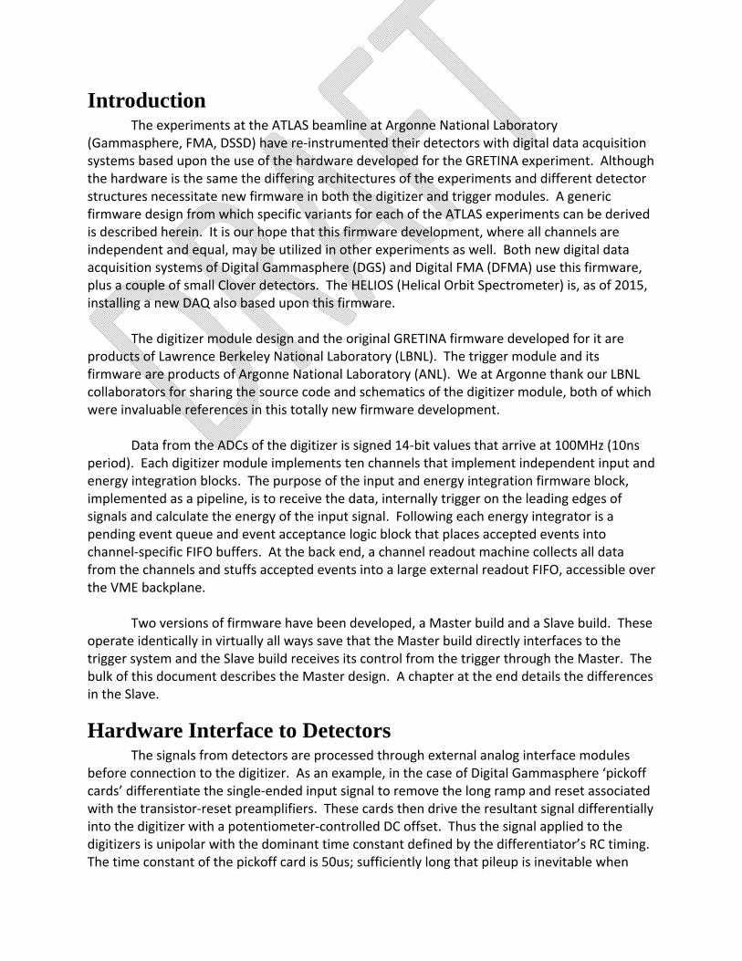
Pileup Detection Logic Pileup recognition is implemented by use of a delay equal to the settings (“m” + “k”) that can hold multiple discriminator firing marks and a counter in a small state machine. The counter is incremented each time the discriminator fires. When the delayed copy of a discriminator firing falls out of the delay, the counter is decremented. Thus the counter continuously tracks the number of pulses stacked up on top of each other over the pileup time. When the counter performs a decrement that makes it fall back to zero, this is indicative of either the end of a pileup train or a non‐piled‐upon pulse. Pileup is determined by whether the counter value exceeded 1 before falling back to zero. Figure 12 shows how this works.
Figure 12 ‐ Simulation showing operation of pileup counter.
The pileup counter in each channel is a four‐bit counter. For exceptionally odd choices
of the various delay settings (e.g. a value of "m" > 16 times the total pulse rise time, coupled with a low discriminator threshold) it is possible that more than 16 pulses may pile up across the summation buffer. In this exceptional case, since the pileup counter has overflowed, the channel pileup logic will seize up into a pileup overflow state. This state is detectable by reading status bits in the master status register, requiring software or user intervention to reset the channel logic and the pileup counter.
Relationship between discriminator hold-off and pileup times There is an important and intimate relationship between the hold‐off time and the pileup time. As explained in greater detail later in the section on Event Readout, there exists a buffer FIFO called the Putative Event Header Queue (PEHQ) that holds the headers of all events sampled by the discriminator. Due to pileup rejection, not every event that enters the PEHQ survives to readout. The PEHQ is loaded when the discriminator hold‐off time elapses. The PEHQ is read at the end of the pileup time (“m” + “k”). If the user sets the pileup time less than the hold‐off time, the order of operations in the PEHQ is upset and all event headers will be filled with erroneous information. Should this occur, the firmware will attempt to protect the user by
a) Setting the ANY_PU_TIME_ERROR bit in the master logic status register; and b) Blocking the assertion of the internal ACCEPTED_HIT and EVENT_EXTENDED signals
within the affected channels so that no events will be available for readout.
0
100
200
300
400
500
600
700
800
9500 14500 19500 24500 29500 34500 39500
InputSignal
DISCBIT
Pileup count*100, 0 at 500
Pileup Detectedwhen count > 1
Pileup Clearedwhen count = 0
<== Pileup Delay ==>
<== Pileup Delay ==><== Pileup Delay ==> <== Pileup Delay ==>
<===IN PILEUP==>

Control and monitoring software should check the ANY_PU_TIME_ERROR bit and inform the user to take corrective action should this condition occur. The ANY_PU_TIME_ERROR bit is automatically cleared each time channel parameters are changed, and then immediately set in any channels whose parameters are set incorrectly.
Trigger Delay Buffer The detection of pileup imposes a delay of "m"+”k” upon the discriminator bit as
reported to the trigger system because the firmware can be set to accept or reject piled‐up pulses. Thus, even though the discriminator fires when then rise crosses the "d" buffer, the event can only be marked as valid or invalid (due to pileup) "m"+”k” clocks later. At this time signals are sent to the external trigger system indicating which channels have fired. By the time the trigger system has been alerted of discriminator activity the edge of the pulse has progressed to be within the Pre‐rise delay buffer. To allow for the use of an external trigger system that can make accept/reject decisions based upon a collection of pileup‐modulated discriminator bits from multiple channels, a delay is required.
The Trigger Delay Buffer is a fixed‐length 20.48us delay buffer that defines the amount
of time after the pileup‐modulated discriminator bit is asserted before an external trigger system must make a decision. If no external trigger is used (“internal” mode), the delay still exists but all events are pre‐marked as selected for readout immediately upon assertion of the pileup‐modulated discriminator bit.
Effects of delayed discriminator bit formation Combined with the other delays, the pileup‐modulated discriminator bit often does not arrive at the trigger system until 10us or more after the edge actually enters the digitizer. There is a delay of “m” + “k” before the edge reaches the discriminator, then the second delay of “m”+”k” after the discriminator fires before the discriminator bit is reported to the trigger. This can cause confusion when attempting to correlate events with other detectors that may not have buffered data acquisition systems and requires careful consideration. While it is easy to implement a delay to use the other detector to gate decisions within Digital Gammasphere, it is not so easy to trigger non‐buffered detectors with Digital Gammasphere unless the fast, coarse discriminator is used.
This long delay may be seen by some as an architectural disadvantage, but the
architecture has the advantage of being able to run at very high event rates. The only dead time imposed by the architecture of this firmware is the discriminator hold‐off time; event rates in excess of 100kHz have been demonstrated in the field (400kHz in the lab) and event rates approaching 1MHz should be achievable.
Baseline Measurement We define the term baseline to be the value of the input signal when no pulses are
being received; this is the combination of DC offset plus any low frequency (e.g. 60Hz) pickup. While the leading‐edge (slope) discriminator function does not care about the baseline, as it

only looks at relative slope, calculation of the energy for any given input signal obviously does due to pole‐zero considerations. Measurement of the baseline value may only be obtained when the input is “quiet” – that is, no discriminator firings. Armed with the knowledge of the dominant time constant of the input signal (that is, the decay time of the pulses) a state machine can determine when the input is likely to be at or near baseline by simply resetting a timer each time the discriminator fires. With the timer set to a reasonable multiple of the dominant time constant the state machine can accumulate samples at any time that the discriminator hasn’t fired for a long enough time that the input may safely be assumed to be at baseline. An accumulator/divider of an integer power‐of‐2 number of samples then suffices to provide a running baseline estimate. In short, this is a digital track‐and‐hold.
A 24‐bit value RUNNING_BASELINE_SUM continuously accumulates all samples across
the first 10.24us of the Trigger Delay buffer, forming a low‐pass filtered version of the input signal. As ADC samples are 14‐bit values and 10.24 is 2 raised to the 10th power, the RUNNING_BASELINE_SUM need be 24 bits to not overflow under any circumstances. At power up the baseline reverts to an initial baseline value defined by the user in a register (multiplied by 1024) and immediately begins tracking from there until the discriminator fires. A timer with a timeout period equal to a user‐programmable integer number of 10.24 microsecond loops is employed. Each time the discriminator fires the timer is reset so that the baseline value is updated only after no discriminator firing has occurred for the full timeout period. When the timer expires, updates of the baseline value may again occur.
Updating of the baseline is performed by taking each 10.24us long accumulation of
samples and comparing the upper 14 bits of that 24‐bit sum against a 14 bit internal baseline value. A secondary counter that initializes to its midpoint value is incremented or decremented based upon the result of that comparison. Should the counter increment or decrement past a power‐of‐two multiple, from 0 to 7 as set by the user, the internal baseline value is then incremented or decremented by one. This multiplies the filtering effect of the 10.24us accumulation method by limiting the slew rate of change to one count every (2^n * 10.24) microseconds. When an event is read out of the digitizer, two baseline numbers are provided:
1. The latest 24‐bit RUNNING_BASELINE_SUM value available before discriminator
activity stopped baseline sampling; to convert to ADC count values, divide this number by 1024.
2. The slowly tracking baseline (based upon the limited slew rate counter) is provided as a 14‐bit number (same range as recoded ADC values).
When no pileup is present it is expected that the two baseline values will be highly similar if not identical. Under high event rate conditions, however, the first number is expected to be a rough guess of the baseline "at the moment" as opposed to the second that would be better interpreted as the "asymptotic baseline if there were no events". While not calibrated, comparison of the first versus the second may provide some indication of baseline drift when

resistively coupled preamplifiers are used. Alternatively, when pileup is present, the difference between the “at the moment” and “asymptotic” baseline values can be used in concert with discriminator firing times to estimate pole‐zero effects. If the power‐of‐two filtering value is set too large, or if the delay after discriminator firing before tracking is re‐enabled is set too large, the highly filtered 14‐bit baseline value may never adjust away from the initial baseline value provided by the user. A diagnostic counter is provided to monitor the number of baseline updates per unit time, so that this condition may be diagnosed.

Event Collection and Readout The structure of the ANL digitizer firmware for event collection and readout differs significantly from the readout system implemented in the LBNL version of the digitizer. In the ANL firmware, every channel is processed as an individual entity with individual pileup, triggering and readout state machines. The overall structure of the readout system is shown in Figure 13.
Figure 13 ‐ Channel readout structure
Event Queuing Some explanation of the elements of Figure 13 is needed. The Channel Delay Chain section is the same logic that has been described previously and shown in Figure 1. In Figure 13 we now add the Putative Event Header Queue (PEHQ), the Pending Event Queue (PEQ) and the Event Header FIFO (typically not abbreviated). The PEHQ (pronounced “peck”) is responsible for storing all event headers from every firing of the discriminator so that no header information is lost during pileup. Such headers may not be needed if the events associated with them are rejected due to pileup, thus they are deemed putative. If an event survives pileup rejection, the header is copied from the PEHQ to the Event Header FIFO. The Event Header FIFO holds event headers until the event is read out by the Channel Readout Controller, or until the event expires.
The PEQ (pronounced “peek”) is responsible for storing the timestamps of every event surviving pileup rejection whose waveform is currently contained within the 20.48us Trigger Delay Buffer. The PEQ allows additional sub‐selection of events by an external triggering system. Flag bits from the PEQ tell the Channel Readout Controller whether to process or discard events as they become available. It is important to understand that waveform data from multiple events may reside within the 20.48us depth of the Trigger Delay Buffer at any moment. The "Accepted Hit" and "Extended Event" bits are asserted to mark the start of each event as they fall out of the Trigger Delay Buffer. This enables high rate operation, but can
Channel Delay Chain
Discriminator
Peak Detect
Pileup Logic
PEHQ LATCH
PEHQ
FIFO
PEHQState Mach
Event Header Data
Pending Event Queue
PEQState Mach
Discriminator Bit
Event Expired
External Trigger Accept & flags
Disc.TimeStamp
TS of pending event
EventHeaderFIFO
Accepted Hit
Extended Event
Trigger Delay Buffer
Waveform Samples
Type, Accept/Reject
REData
ChannelReadoutController
DataFIFO
ToBoard-widedata mux

result in conflict between event rate and the parameters for readout set by the user. Careful setting of readout parameters is necessary for optimal operation at high rates; if excessively long waveform data is requested events may interfere with each other and result in the loss of some events. Please refer to the section on Readout Interference, below.
Use of the Pending Event Queue (internal vs. external triggering) Each channel of the ANL digitizer may be individually set to be in either Internal or External trigger mode. The External mode is often referred to as the “TTCL” mode (“TTCL” being a GRETINA acronym for Trigger, Timing and Control Logic). In the Internal mode, the PEQ is bypassed and all events are immediately accepted and immediately tagged for readout. The header is immediately copied from the PEHQ to the Event Header FIFO and readout begins based upon the timestamp.
In the External mode, the PEQ holds the timestamps of all events currently held within the Trigger Delay Buffer. During the time that event timestamps reside within the PEQ, messages from the trigger system are received that indicate acceptance occurring at a certain timestamp. When these messages are received, the entire PEQ is searched and any events whose timestamp falls within a window of time around the timestamp value in the acceptance message are marked for readout. As each event becomes available for readout only those that have been marked as accepted are actually transferred to the board‐wide FIFO.
Waveform Readout Generalities When an event is accepted for readout the timestamp of the discriminator firing is available in the Event Header FIFO and the current timestamp is also known. A programmable waveform readout offset is applied to the timestamp in the Event Header FIFO, adjusted for the length of the Trigger Delay Buffer and then compared to the current timestamp. When a match is made readout commences for a programmable length. As there is no enforced correlation between the pileup time and the readout length it is possible that an event becomes available for readout before the readout of the previous event is complete. This can result in a dropped event, one that could not be read out. Each channel of the digitizer has four counters that monitor channel activity; one of them counts dropped events and should be monitored at all times.
Data Collection across the Digitizer and Readout over VME Readout of each channel fills a channel‐specific FIFO. A second readout state machine continuously scans the holding FIFOs filled by the channel readout machines. When a channel FIFO indicates that a full event is available the board‐wide machine transfers that event from the memory inside the FPGA to the large external FIFO memory read out by VME. No partial transfers ever occur; only whole events are transferred. Only one event is transferred from a given channel at a time; when one event from a channel is completely transferred the machine searches for the next channel with an available event even if additional events may be available in the current channel.

This round‐robin method insures that one busy channel can't block data from the other channels, but may result in dropped events if the one busy channel fills its channel‐specific FIFO and then has another event before the readout selector is able to circulate back to the busy channel again. In the end this is a bandwidth management issue controlled most strongly by the amount of waveform data the user has selected to read out per channel. Firmware built after May 20, 2014 partially addresses this issue by doubling the size of the Accepted Event FIFO so that it can store two full‐sized (1024 sample) events before it goes full. In a VME system read out by a typical embedded processor board the total backplane bandwidth will be on the order of 10Mbytes/sec after accounting for monitoring overhead plus the inefficiencies of polling & reading out multiple digitizer boards. The total bandwidth should be divided by the total number of channels to estimate the bandwidth available per channel. Assume a crate with four digitizers within it; 10MByte/sec divided by 4 allows only 2.5MByte/sec of bandwidth per digitizer on average.
Worst‐case event rates without dropped events may then be estimated, using the
scenario in which all channels within a digitizer are hit simultaneously and the user has selected maximum waveform readout length in all channels. An event with full waveform readout is approximately 2100 bytes, including the header. At 2.5MByte/sec, an event of that size takes 840usec to read out from each channel. With every channel hit, then, the round‐robin can’t get back to a channel once read for 8.4 milliseconds. With single buffering the Accepted Event FIFO can handle one event in 8.4msec (119Hz) but with double‐buffering twice that rate can be supported in the worst‐case scenario. Such worst‐case situations are unlikely in any practical experiment. It is more likely that in a practical experimental situation only a few percent of channels will be simultaneously hit. Assuming a channel occupancy 10%, but with every digitizer module in the crate still being hit every time, with double‐buffering the full‐length readout will support event rates of approximately 2.4kHz. With a more practical waveform readout length of 100 samples per event rather than the maximum of 1024, a much more useful event rate of 24kHz is achieved.
Waveform Decimation Often experimenters desire to have waveform readouts spanning a greater amount of
time, but the full 100MSamp/sec sampling rate is excessive. To accommodate this, “decimator” logic is provided in the channel‐level readout machine. A programmable data reduction factor from 0 to 7 is available. The data reduction factor selects a power‐of‐two data reduction (0=all, 1=reduce by factor of two, 2=reduce by factor of four, etc.). Data reduction is accomplished by averaging together the selected number of full speed data samples and then writing the average‐of‐n every nth clock. The result is that the length in time covered by the waveform buffer doubles for each successive data reduction factor. At the maximum setting, a full length (1024 sample) readout spans 10.24us * 128, or 1.31 milliseconds.
At present data reduction is applied to the entire waveform readout without respect to
any edges that may be contained therein. In a future release we intend to implement “smart” data reduction that would compress all samples except for small regions containing discriminator firings that would be preserved at full sampling speed.

Pileup and Event Readout The ANL digitizer handles pulse pileup at three levels. The first level of logic is at the channel level where events are accepted or rejected. If a channel is set to reject piled‐up events neither the readout logic nor the trigger system knows that these pileup events occurred. However, the coarse discriminator will always report found edges irrespective of pileup settings. A second level of pileup control occurs at the readout machine level. This logic necessitates a bit of terminology. We define events leaving the channel logic and entering the readout logic as being either accepted or extended.
When pileup rejection is on, all events proceeding to the readout logic are, by definition, not piled up. Such events are all flagged as “accepted” events.
When pileup rejection is off, only the first event in a string of piled‐up events, or any isolated and non‐piled event, is accepted; all subsequent events in a piled‐up string are marked as extended events.
By definition extended events can only occur following an accepted event. The ACCEPTED_HIT signal is the source of the delayed signal EVENT_EXPIRED that removes events from being accepted for readout by an external trigger system. Thus the PEQ only contains the timestamps of accepted hits.
The third level of pileup control occurs based upon a pileup flag stored in the header of all accepted events. The readout machine may be set to only read out those accepted events that have the pileup bit set, resulting in only piled up events showing up in the readout and all other events suppressed.
Readout Interference When the readout length of one event overlaps the data from the next event there is
risk of readout interference. This situation usually arises when the selected readout length is longer than the accumulation buffer depth. Figure 14 shows an example waveform highlighting the effects of pileup and selected waveform readout length. In Figure 14, four pulses cause four discriminator firings and, thus, four events. The timing between the firings, when compared to the depth of the summation buffer “m”, causes events #2 and #3 to be piled upon one another. However, the waveform readout depth selected by the user causes the readout of event #1 to interfere with that of event #2. The lower portion of Figure 14 shows the events on a timeline showing when each event would ideally read out. This timeline will be repeated in the following sections to explain how the various modes affect the readout.

Figure 14 ‐ Example waveform for describing pileup readout modes
Readout Interference when Decimation is in use It is critically important to understand that the use of waveform decimation has a direct impact upon readout interference. With waveform decimation enabled, once readout of an accepted event occurs, the longer physical time spanned by the decimated readout will inevitably result in a higher number of following events being contained in the waveform readout from the first event. In the default readout mode of No Offset, use of significant decimation factors will typically result in many events contained in waveforms that have no headers. Generally, if the DAQ system can handle variable event sizes, use of the Offset with Truncation readout mode is considered best when decimation is activated.
Pileup Extension and Readout Modes When Pileup Extension is disabled the readout logic is constrained to process only accepted events. This means that isolated events (no pileup) and the first event of a pileup train may potentially be read out, but that the 2nd and later events within a pileup train (the extended events) will all be discarded. When Pileup Extension is enabled the readout logic is may process all events, accepted or extended. The default state is disabled. Separately, the user may select one of four possible event readout modes, named No Offset, Offset, Offset with Truncation and Header Only. These four modes operate in slightly different ways depending upon whether Pileup Extension is enabled or disabled so the combination of the Pileup Extension and Readout Mode controls effectively generate eight different readouts. The two sections below describe how each of the four readout modes will operate in each of the two Pileup Extension states.

Readout Modes when Pileup Extension is Disabled In the event example shown as Figure 14, Event #2’s start occurs before the entire
readout of Event #1 is complete, setting up a situation where readout interference occurs. Because Event #3 is an extended event – being the 2nd pulse in the pileup group – it will never be read out in any of these cases because Pileup Extension is disabled. If the pileup train were longer (additional events between #3 and #4), these would also be extended and thus excluded from the readout. Each of the four readout modes will react differently to the readout interference condition, as summarized in Table 1.
Extension Mode
Name Operational Description
00 No Offset If the readout length of any event overlaps with the data of a later event, the later event is lost.
01 Offset If the length of the readout of an event causes that readout to extend past the start of the next, a second header will be issued and a 2nd full buffer of samples will be read out for the 2nd event, even though the leading edge of the 2nd event may be found in the 1st event’s waveform data or may span both buffers. Offset continues to accumulate until the amount of offset exceeds the length of the readout machine’s accepted event FIFO. Should this occur the next event is dropped.
10 Offset with
Truncation
If the length of the readout of one event causes that readout to extend past the start of the next, readout of the later event starts immediately after the first one. The total length of waveform data in the 2nd event is shortened so that only additional waveform data past the overlap point is read out. This results in a total readout length of the following event that is variable.
11 Header Only
If the length of the readout of one event causes that readout to extend past the start of the next, only the header of the overlapping event is read out and no waveform data in the 2nd event is provided.
Table 1 ‐ Modes of readout with Pileup Extension DISABLED
Figure 15 provides a visual demonstration of these effects. The No Offset mode prevents readout of Event #2 because #2 interferes with the readout of Event #1 already in progress. The other three modes allow some or all of Event #2 to be read out by offsetting the beginning of the readout until the interference is cleared. The Header Only mode provides an alternate solution to readout interference by collapsing interfering events to only headers.

Events (color coded) as they fall out of the 'T' buffer (10.24us delay) ‐ nominal positions if length of waveform readout did not cause interference.
Bold color is header Event #1
remainder represents 10usec of waveform readout Event #2
Event #3
Event #4
When Pileup Extension is disabled, only Accepted events show up in readout. Since Event #3 is Extended, it will never read out.Pileup Extension Enable Waveform Extension Mode
0 00 : No Offset Event #1 Event #4
Events #2 is dropped as the nominal (non‐offset) start of readout would interfere with the readout of the current event.
0 01 : Offset Event #1 Event #2 Event #4
Readout of each Accepted event is delayed until the previous event is finished reading out with no change in packet length.
0 02 : Offset w/truncation Event #1 Event #2 Event #4
Readout of each Accepted event is delayed until the previous event is finished; readout shortened to match non‐offset nominal end time.
0 03 : Header Only Event #1 <== Event #2 ‐ only header Event #4
Readout of each Accepted event is delayed until the previous event is finished; only headers of interfering events are read out.
Figure 15 ‐ Visual representation of the readout modes with Pileup Extension DISABLED
Readout operation when Pileup Extension is Enabled Again using the event example shown as Figure 14, Event #2’s start occurs before the
entire readout of Event #1 is complete, setting up a situation where readout interference occurs. However, because Pileup Extension is now enabled, Event #3 (an extended event) can now be read out. If the pileup train were longer (additional events between #3 and #4), these would also be extended and thus also available for readout. Each of the four readout modes will react differently to the readout interference condition, as summarized in Table 2.

Extension Mode
Name Operational Description
00 No Offset In this mode, both accepted and extended events may be read out but only if the entire event can be read out to the programmed event length before the next event has to be read out. In this mode either accepted or extended events may be discarded because the full readout wouldn’t fit; thus use of this mode is discouraged when Pileup Extension is enabled.
01 Offset If the length of the readout of an event causes that readout to extend past the start of the next, a second header will be issued and a 2nd full buffer of samples will be read out for the 2nd event, even though the leading edge of the 2nd event may be found in the 1st event’s waveform data or may span both buffers. Offset continues to accumulate until the amount of offset exceeds the length of the readout machine’s accepted event FIFO. Should this occur the next event is dropped.
10 Offset with
Truncation
If the length of the readout of one event causes that readout to extend past the start of the next, readout of the later event starts immediately after the first one. But, the total length of waveform data in the next event is shortened so that only additional waveform data past the overlap point is read out. This results in a total readout length that is variable; however, this is the most efficient format for reading out piled‐up waveforms.
11 Header Only
If the length of the readout of one event causes that readout to extend past the start of the next, only the header of the overlapping event is read out. If any event can be read out in full, it will be.
Table 2 ‐ Readout modes with Pileup Extension ENABLED
As in the previous section, Figure 16 provides a visual demonstration of these effects. The No Offset mode prevents readout of Event #2 because #2 interferes with the readout of Event #1 already in progress; however, Event #3 can be read out is it does not interfere. This potential of skipping the accepted event while allowing through some or all of the extended events associated with the missing accepted event is why we discourage the use of the No Offset mode when Pileup Extension is enabled. Please note that the Header Only mode only collapses interfering events into headers, and that such collapse may then free other events to be read in full.
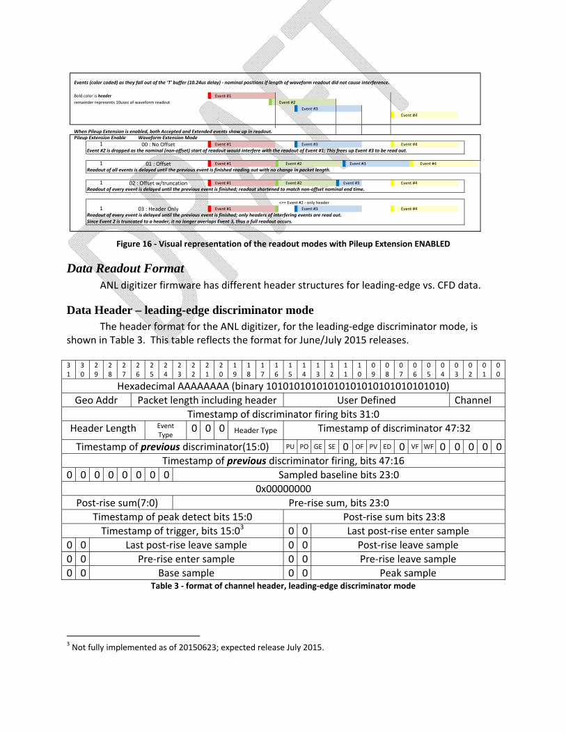
Events (color coded) as they fall out of the 'T' buffer (10.24us delay) ‐ nominal positions if length of waveform readout did not cause interference.
Bold color is header Event #1
remainder represents 10usec of waveform readout Event #2
Event #3
Event #4
When Pileup Extension is enabled, both Accepted and Extended events show up in readout. Pileup Extension Enable Waveform Extension Mode
1 00 : No Offset Event #1 Event #3 Event #4
Event #2 is dropped as the nominal (non‐offset) start of readout would interfere with the readout of Event #1; This frees up Event #3 to be read out.
1 01 : Offset Event #1 Event #2 Event #3 Event #4
Readout of all events is delayed until the previous event is finished reading out with no change in packet length.
1 02 : Offset w/truncation Event #1 Event #2 Event #3 Event #4
Readout of every event is delayed until the previous event is finished; readout shortened to match non‐offset nominal end time.
<== Event #2 ‐ only header
1 03 : Header Only Event #1 Event #3 Event #4
Readout of every event is delayed until the previous event is finished; only headers of interfering events are read out.Since Event 2 is truncated to a header, it no longer overlaps Event 3, thus a full readout occurs.
Figure 16 ‐ Visual representation of the readout modes with Pileup Extension ENABLED
Data Readout Format ANL digitizer firmware has different header structures for leading‐edge vs. CFD data.
Data Header – leading-edge discriminator mode The header format for the ANL digitizer, for the leading‐edge discriminator mode, is shown in Table 3. This table reflects the format for June/July 2015 releases. 31
30
29
28
27
26
25
24
23
22
21
20
19
18
17
16
15
14
13
12
11
10
09
08
07
06
05
04
03
02
01
00
Hexadecimal AAAAAAAA (binary 10101010101010101010101010101010)
Geo Addr Packet length including header User Defined Channel
Timestamp of discriminator firing bits 31:0
Header Length Event Type
0 0 0 Header Type Timestamp of discriminator 47:32
Timestamp of previous discriminator(15:0) PU PO GE SE 0 OF PV ED 0 VF WF 0 0 0 0 0
Timestamp of previous discriminator firing, bits 47:16
0 0 0 0 0 0 0 0 Sampled baseline bits 23:0
0x00000000
Post‐rise sum(7:0) Pre‐rise sum, bits 23:0
Timestamp of peak detect bits 15:0 Post‐rise sum bits 23:8
Timestamp of trigger, bits 15:03 0 0 Last post‐rise enter sample
0 0 Last post‐rise leave sample 0 0 Post‐rise leave sample
0 0 Pre‐rise enter sample 0 0 Pre‐rise leave sample
0 0 Base sample 0 0 Peak sample Table 3 ‐ format of channel header, leading‐edge discriminator mode
3 Not fully implemented as of 20150623; expected release July 2015.

Many items are clear from the names, but a few entities should be explained:
The Header Type field is a four‐bit code indicative of which format of header this is. By fiat, a header type of 0000 is the GRETINA format.
o ANL digitizer firmware versions released prior to May 2015 have been assigned type 1 for leading‐edge discriminator data, and type 2 for CFD discriminator data. Table 3 in this document does not match these earlier versions; see earlier releases of this document for that format.
o ANL digitizer firmware to be released in June/July 2015 has been assigned type 3 for leading‐edge discriminator data, and type 4 for CFD discriminator data. Table 3 matches these releases only.
The Event Type field is a three‐bit field that indicates which trigger system algorithm selected this event, if the digitizer is being run in TTCL mode. If the digitizer is being run in Internal mode, the Event Type is “000”.
The ‘PU’ bit in the 5th word of the header is the Pile Up flag; if set this indicates that the event being recorded was either piled upon by a following signal or itself piled up on a previous signal.
The ‘PO’ bit in the 5th word of the header is the Pile Up Only flag; if set this indicates that only piled‐up events are being read out, as selected by the user.
The ‘GE’, or General Error bit, is set if the Pending Event Queue has been overrun.
The 'SE', or Sync Error bit, is set if grievous timestamp mismatches with the trigger system have been noted.
The ‘OF’, or Offset Flag bit, is set if this event has been offset by the readout logic (and thus, the waveform does not start at the expected place).
The ‘PV’ bit in the 5th word of the header is the Peak Valid flag; if set this indicates that the timestamp and sample data in words 10 and 14 is valid. If not set, this indicates that the peak detector logic failed to find a peak in the pulse.
The 'ED', or External Discriminator bit, is set if this event has been caused by an external discriminator override as opposed to an event from the normal operation of the discriminator within the channel itself.
The ‘VF’, or Veto Flag bit, is set if this event was marked for vetoing by the trigger logic, but the vetoing of events by the trigger was disabled in the digitizer by the user and thus the event was read out. This bit is associated with the Digital Gammasphere “clean‐dirty” logic.
The ‘WF’, or Write Flags bit, is set if the “timing mark” flags for discriminator firings and peak detection are being added to the waveform portion of the data.

Data Header – CFD mode The header format for the ANL digitizer, for the CFD build, is as shown in Table 4. 31
30
29
28
27
26
25
24
23
22
21
20
19
18
17
16
15
14
13
12
11
10
09
08
07
06
05
04
03
02
01
00
Hexadecimal AAAAAAAA (binary 10101010101010101010101010101010)
Geo Addr Packet length including header User Defined Channel
Timestamp of discriminator firing bits 31:0
Header Length Event Type
0 0 0 Header Type Timestamp of discriminator 47:32
Timestamp of previous discriminator(15:0) PU PO GE SE CV OF PV ED TSM VF WF 0 0 0 0 0
0 0 CFD Sample 0 0 0 previous discriminator TS, bits 29:16
0 0 0 0 0 0 0 0 Sampled baseline bits 23:0
0 0 CFD Sample 2 0 0 CFD Sample 1
Post‐rise sum(7:0) Pre‐rise sum, bits 23:0
Timestamp of peak detect bits 15:0 Post‐rise sum bits 23:8
Timestamp of trigger, bits 15:04 0 0 Last post‐rise enter sample
0 0 Post‐rise end sample 0 0 Post‐rise begin sample
0 0 Pre‐rise end sample 0 0 Pre‐rise begin sample
0 0 Base sample 0 0 Peak sample Table 4 ‐ format of channel header, CFD build
The CFD header has a few differences with respect to the leading‐edge header.
The Header Type field is a four‐bit code indicative of which format of header this is. o ANL digitizer firmware versions released prior to May 2015 have been assigned
type 1 for leading‐edge discriminator data, and type 2 for CFD discriminator data. Table 3 in this document does not match these earlier versions; see earlier releases of this document for that format.
o ANL digitizer firmware to be released in June/July 2015 has been assigned type 3 for leading‐edge discriminator data, and type 4 for CFD discriminator data. Table 3 matches these releases only.
The "CV" flag indicates CFD Valid. This bit is set if the CFD equation found a crossing and latched timestamp data. In the leading‐edge mode this bit is always 0.
The "TSM", or Time Stamp Matched, flag indicates whether bits 47:30 of the timestamp of this event matched bits 47:30 of the timestamp of the Last Discriminator Timestamp value. This flag is required, as the CFD format of the header has reduced the number of bits assigned to the Last Discriminator Timestamp field.
The three CFD Sample values are signed objects that are the result of the subtraction of the digital CFD equation result from the 'local zero' value. CFD Sample 0 is the sample associated with the sign crossing, whereas CFD Samples 1 and 2 are the two previous samples of this subtraction. 4 Not fully implemented as of 20150623; expected release July 2015.

Waveform Data Format Details In the ANL firmware, the 14‐bit data samples are reported as 14‐bit unsigned offset binary rather than signed binary, such that a value of “00000000000000” indicates a sample at the most negative voltage the ADC can measure. A value of “11111111111111” indicates a sample at the most positive voltage the ADC can measure. Additionally the ANL firmware reserves the two most significant bits of each 16‐bit value, as shown in Table 5. One is used as the timing mark and the other is reserved for later use. 31
30
29
28
27
26
25
24
23
22
21
20
19
18
17
16
15
14
13
12
11
10
09
08
07
06
05
04
03
02
01
00
M 0 ADC DATA SAMPLE M 0 ADC DATA SAMPLE Table 5 ‐ Format of waveform data
The “M” bits are timing mark bits. These bits are set to indicate the samples associated with discriminator or peak detector firing. The timing mark bit encodes what information is being marked by the number of samples the mark is asserted:
A mark bit that is one sample long indicates the time that the leading‐edge discriminator fired. In CFD mode that indicates when the CFD was armed.
A mark bit that is two samples long indicates different information dependent upon the mode the digitizer is operating in:
o In the leading‐edge mode, the two‐sample mark indicates the time at which the leading‐edge discriminator hold‐off time elapsed.
o In the CFD mode, the two‐sample mark indicates the time at which the CFD fired.
A mark bit that is three samples long indicates the peak detector firing time in both leading‐edge discriminator and CFD modes.
The timestamp of the discriminator firing as recorded in the header is the timestamp at which the discriminator of the selected mode actually fired (leading‐edge or CFD).

Interface to the external trigger The ANL firmware implements a SERDES link between digitizer and trigger system in a manner similar to that used in GRETINA, but data issued by the digitizer has a significantly different format. On the receive side, the digitizer receives the control stream from the trigger and synchronizes itself to the clock from the trigger and to the timestamp as broadcast by the trigger. The firmware responds to the command frames defined in the Trigger Timing and Control Link specification as originally written for the GRETINA experiment, plus many additions made for multiple detectors and cross‐triggering unique to the Digital Gammasphere version of the trigger firmware. Specific features of the digitizer firmware related to the triggering system are discussed in this section.
Timestamp Synchronization The ANL digitizer uses a reception state machine similar to that of the Router trigger implementing the 'stringent lock' feature. All fixed values within the command stream may be monitored for more stringent checking of data validity. In addition, enhanced timestamp synchronization logic is implemented. The digitizer resets its timestamp upon receipt of Imperative Sync commands but also uses the non‐imperative Sync commands to compare against the local timestamp counter. Mismatches between the timestamp value in the Sync command are assumed to be data transmission errors rather than counter errors. For a singular mismatch, the local timestamp is maintained and the trigger's timestamp is ignored. If three mismatches in a row occur, it is assumed that there is a serious communications error and a status bit is set in a register so that slow controls may alert the user to the problem.
Event Veto Provision is made for an Event Veto input from the trigger for each channel. The Event Veto is enabled by register bits within the digitizer. If this function is enabled the most recently entered value in the Pending Event Queue is erased should the trigger assert the Event Veto bit for a given channel. This feature requires relatively tight timing; any such veto must be issued before the next pulse places an entry into the Pending Event Queue. Fortunately, only Accepted events add data to the Pending Event Queue, so a delay of a couple microseconds should always be available with normal pileup settings. The Event Veto is intended for use in concert with the external triggering system. In the specific case of Digital Gammasphere, two channels of each digitizer are associated with the Ge Center and BGO Sum signals of a given detector. Digital Gammasphere detectors are intended to be run in "clean" (Ge hit without corresponding BGO), "dirty" (Ge and BGO) or "module" modes (Ge or BGO), but the hits are not coincident in time. By use of the Event Veto function, the Router modules of the external trigger may monitor the channel pairs, implement the time window and issue commands to Veto the events that are "dirty" or "module" if only "clean" events are desired. There is no provision to go back and Veto an older event deeper in the PEQ. As the PEQ only contains Accepted events, a Veto by definition suppresses any and all Extended events associated with the vetoed event and thus suppresses an entire train of piled‐up pulses.

In the Digital Gammasphere version of trigger firmware, the Router trigger modules independently calculate the Event Veto bits for the digitizers each serves to minimize latency. The Veto bits themselves are inserted by the Routers into the 5th word of each Trigger Timing and Control frame on the fly, without any intervention by the Master Trigger. As channel pairs are vetoed by the Router boards, internal “Clean multiplicity”, “Dirty multiplicity” and “Module multiplicity” sums are continuously updated. Any two of these per‐Router partial sums may be selected for transmission to the Master Trigger. The Master Trigger forms the system‐wide multiplicity sums and may then issue trigger acceptance commands based upon these sums.
The Veto process is optionally enabled by the user, so that raw multiplicities may always
be used in place of the Clean, Dirty or Module sums. In non‐Veto modes mapping registers within the Router trigger boards allow each discriminator bit to be optionally mapped into the “X‐plane” or “Y‐plane”, allowing the same firmware to service the dual‐sided silicon strip detector of DFMA.
Trigger Decision Latency The trigger will not respond to all events with the same time delay. This is caused by two factors:
1. Each different trigger algorithm that may be coded will have a different trigger formation time that we will name Ttf.
2. The 2us system cycle of the Trigger Timing and Control link means that there is an additional delay of from zero to 2us after Ttf before the trigger accept message can be transmitted; then of course there is the risk that in a high rate experiment triggers could back up in the FIFOs of the trigger system causing occasional delays of 0‐4us before transmission.
Details of the trigger window calculation When a trigger acceptance message is received, all event timestamps in the PEQ are
compared against the timestamp value contained within the trigger message. A bit of math is required. The timestamp reported by the trigger is the time at which the trigger module determined that a trigger algorithm was satisfied. If an event occurs at time T0, the trigger will respond at a variable time Ttf later. When processing the events in the pending event queue the timestamps in that queue are the time of the leading edge (T0).
Upon receipt of the trigger message, the timestamp of the trigger message is subtracted
from the timestamp of the firing within the pending event queue for every firing within the queue. Under normal conditions where the trigger is formed from multiplicity, this will always yield a negative number. However, if the trigger is caused by a different detector that may be faster than the one connected to the digitizers, a positive answer may result. The answer is compared against the upper and lower time window registers (< upper, > lower) and if both comparisons are valid, the event is accepted for readout.

The method of subtraction used means that the window is defined with respect to the time the Master trigger detected the appropriate condition and not the time of the discriminator firing. That is, if there were an oscilloscope connected to the discriminator signal and also to the trigger signal5, and the oscilloscope were triggering on the signal from the trigger system, discriminator firings would be seen in a range of times prior to the trigger signal. Thus, the correct settings for the two window registers would also be negative, with the ‘min window’ register set to the relative time of the earliest (farthest back from the trigger) discriminator firings and the ‘max window’ set to the relative time of the latest (closest to the trigger) discriminator firings. This apparent reversal of “min” and “max” is because the logic always requires that the “max” window edge be later in absolute time than the “min” position. See Figure 17.
Figure 17 ‐ Trigger windows within the digitizer
For an accumulation window “m” of 4usec and a “k” window of 0.6usec, the
discriminator bit will be sent to the trigger system 4.6usec after the discriminator actually fires due to the channel pileup logic. It will take approximately 0.75usec for the message to propagate through the SERDES link to the Router trigger board and then again for the Router data to propagate to the Master Trigger. Thus the expectation is that, for locally‐generated triggers (e.g. multiplicity), the timestamp in the trigger acceptance message will be approximately “m”+”k”+ 0.75us after the timestamp of the actual discriminator firing. The acceptance windows should then be set to –(m+k) and –(m+k+1.5us) to insure collection of the appropriate events.
5 Usually available by setting the NIM output of the Master Trigger to the ANY_TRIG setting.
T0 - time ofdiscriminator firing
Time when triggerlatches the decision
Time when triggertransmits the decision
Max Window
Min Window
Events in here are read out

Other Commands from the Trigger Trigger decision commands are processed by the digitizer if the “TTCL” mode is enabled; otherwise they have no effect. The Demand Slow Data command (frame #13) of the trigger’s command stream – used in the LBNL version of the digitizer – has no effect in the ANL version as there is no ‘slow’ data to send; in Gammasphere and DSSD all data is ‘fast’. The ANL digitizer is, however, sensitive to commands distributed in the 16th frame. This frame is interpreted as a Synchronous System Capture command that causes diagnostic counters within the digitizer to first reset and then collect counts of various activities within each channel for a period of time defined within the data values of the command.
Information Sent to the Trigger System by the Digitizer By the same token, the lack of the ‘fast’ vs. ‘slow’ data concept as used in the GRETINA version written by LBNL allows for a simpler data format to the trigger system. In the ANL firmware each word every 20ns is a unique message. The data sent every 20ns is simply a snapshot of the state of every channel’s discriminator bit plus the fast, or coarse, discriminator bits from channels 5‐9. The selection of channels 5‐9 for the coarse bits is driven by the specific cable plant of Digital Gammasphere, where channels 5‐9 are connected to the germanium center contacts and channels 0‐4 are connected to the BGO sum signals. By having the fast, coarse, Ge discriminator bits sent to the trigger system prompt multiplicity‐based pre‐triggers may be formed system‐wide. As all channels are reported the Ge/BGO nomenclature is only a convenience for Digital Gammasphere and any other detector system still has all the information from all channels.
The amount of time each discriminator bit is asserted is programmable to insure multiplicity sums are properly calculated. Within the Digital Gammasphere system, where multiple channels of a digitizer are tied to the same detector module, cross‐channel marking or triggering is performed entirely within the trigger.
The choice to send only discriminator bits and not energy values is driven by the specific
architecture of the Digital Gammasphere and Digital FMA systems where all triggers are based upon multiplicities. No energy information is provided to the trigger by the digitizers in these systems as the system designers have concluded that energy‐based triggers are not practical for this detector. There is no provision in the all‐fast data format to add any information other than discriminator data to the data sent to the trigger.
Data Flow Control (Throttle) The digitizer hardware supports two non‐serialized LVDS control signals that run from
the digitizer to the router trigger board. One of these is defined in both GRETINA and DGS firmware as the Throttle bit. This bit is asserted by the firmware whenever the board‐wide FIFO reaches the half full point. The trigger routers collect the Throttle bits from each digitizer and the Master Trigger may suspend the issuance of trigger accept messages while any digitizer is asserting the Throttle bit.

This hardware‐ and firmware‐based rate throttling has been tested and is in common usage in Digital Gammasphere. As of this writing, however, GRETINA digitizers do not use the Throttle bit and instead implement trigger rate control by a software mechanism.

Master and Slave Digitizers A compile‐time build option named SLAVE_MODE allows use of the front bus ribbon cable to connect one digitizer to another in a subservient relationship. The front bus ribbon cable contains a mix of signals with a certain amount of data direction control. The mix of signal types and directions is the same as in GRETINA digitizers, but the definition and usage has been changed:
A differential Clock signal whose direction is controlled, not by firmware, but by hardware jumpers. The Master and Slave boards must have their jumpers set correctly to work as desired. From the firmware standpoint, FBUS_CLK is an input that either is used (Slave) or ignored (Master). The clock sent from the Master to the Slave is the switched 50MHz clock, that when a trigger system is used is the clock received from the trigger via the SERDES link.
Eighteen bits that are used to carry data from the Master to the Slave(s). The lower 17 bits are a direct and immediate copy of the SERDES data that comes from the trigger system. In the Slave digitizer these bits are fed to the SERDES receive state machine in lieu of the data from the Slave’s SERDES chip. The data is DC‐balanced but with the “clock guard” bit removed.
o Bit 17 is a reset bit sent from the Master to the Slave, the same as the Master’s main reset signal.
o Bit 16 of the Master‐to‐Slave data is, instead of the clock guard, a copy of the discriminator bit from channel 0 of the Master digitizer. This bit is one of the four “external discriminator” options. Certain combinations of these modes allow any or all of the channels of a Slave digitizer to be directly driven by the bit from the Master. Due to delay in crossing the cable, the P1 and/or P2 delay buffers of all
channels in the Slave must be adjusted to values a few clocks larger than that of the Master digitizer to synchronize operation.
Three bits are transmitted from the Slave to the Master. o A status flag from the Slave’s external FIFO is sent back to the Master so that the
Master may assert its Throttle Request bit to the trigger if either the Master or the Slave is in danger of FIFO overflow.
o A status bit is sent from the Slave to the Master to indicate that the Slave’s SERDES receiver state machine is locked onto the trigger command stream.
o The third bit is available as a spare.
A “Wire‐Or” bit is also available on the cable that may be used for the Throttle Request feature in cases where multiple Slaves are connected to the Master. This, of course, requires that jumpers and terminations be appropriately set to insure clean data transfer.
These connections are summarized in Figure 18. An important item to note is that the Slave digitizer receives and may respond to any commands sent by the trigger system, but the Slave digitizer has no way to communicate any discriminator information back to the trigger. One

signal is available to provide rate control via the trigger throttle request, but that is the total extent of the Slave’s communication to the trigger system. As such, the trigger is blind to the operation of the Slave and has no ability to consider the Slave’s state in any trigger decision. This differs from the GRETINA model in which there is a slow collection mechanism to collect Slave digitizer discriminator bits when the central contact fires. However, that mechanism does not preserve timing of the Slave bits and cannot detect pileup.
Figure 18 ‐ Connections between Master and Slave digitizers.
Detailed Description of External Discriminator Modes Figure 18 shows that the cable is but one potential source for the External Discriminator signal in the channels of the digitizer. Note that the External Discriminator operation is available in both Master and Slave builds of the ANL digitizer. The source control for the external discriminator allows the user to select from one of four options to define the external discriminator signal:
1. The discriminator bit from Channel 0 of the board. 2. If the digitizer has the Slave version of firmware, a second option is bit 17 of the data
from the front bus cable. In Master digitizer builds, this option is disabled. 3. Auxiliary I/O bit 10 on the front panel. 4. One of six selectable timestamp‐based clocks.
At the channel level, each channel has four options defining that channel’s response to the external discriminator signal:
1. The channel fires based upon its own discriminator logic (default); the external discriminator signal is ignored.
"Master"Digitizer
Bit 17CH 0
CH 1
CH 2
CH 3
CH 4
CH 5
CH 6
CH 7
CH 8
CH 9
DISC BIT
SERDES RXBits 16:0
CH 0
CH 1
CH 2
CH 3
CH 4
CH 5
CH 6
CH 7
CH 8
CH 9
SERDES RX
SERDES_SM_LOCKED
SERDES_SYNC_FLAG
FIFO CTLEXT_FIFO_HFFIFO CTL OR
Throttle to trigger
To status reg.
To status reg.
SERDES fromtrigger
Ext. Disc.
Ext. Disc.
Ext. Disc.
Ext. Disc.
Ext. Disc.
Ext. Disc.
Ext. Disc.
Ext. Disc.
Ext. Disc.
Ext. Disc.
EX
TE
RN
AL
DIS
C M
UX
"Slave"Digitizer
50MHz clock
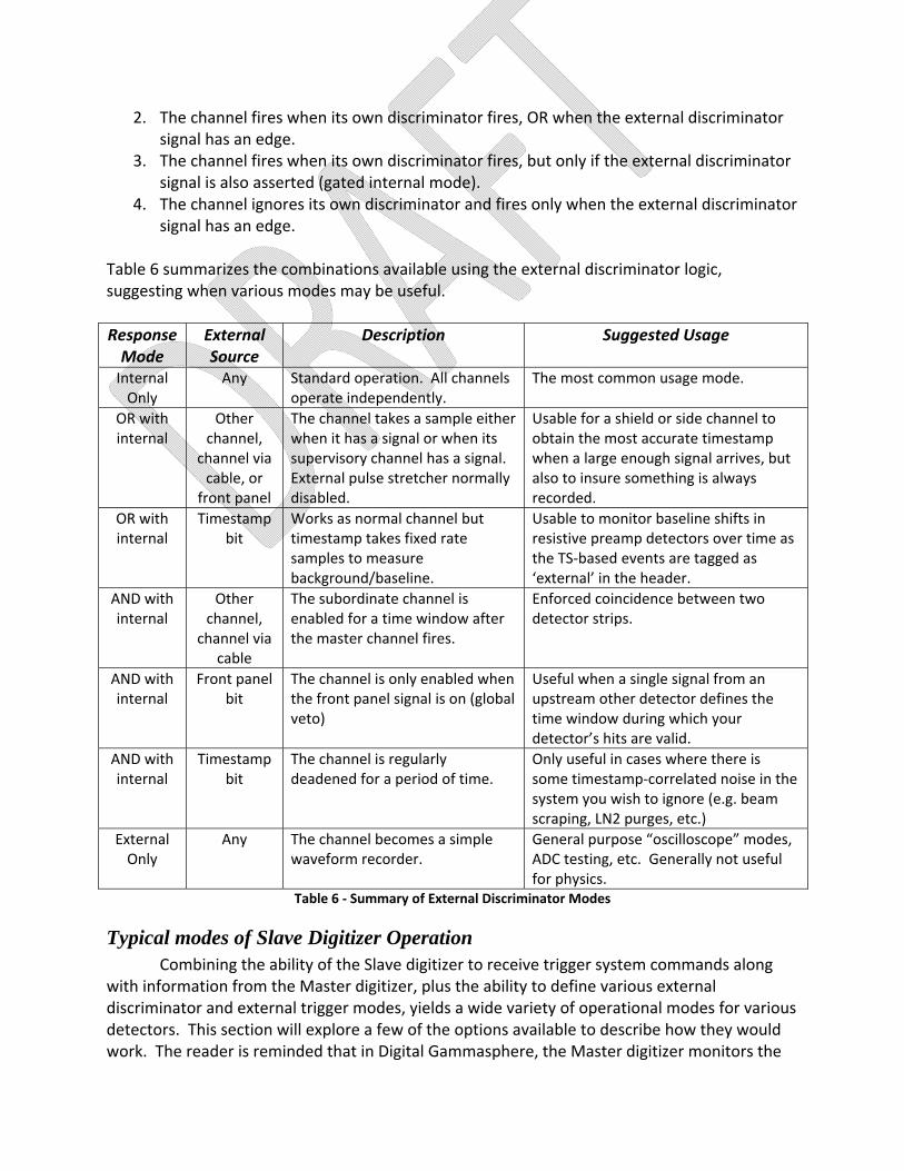
2. The channel fires when its own discriminator fires, OR when the external discriminator signal has an edge.
3. The channel fires when its own discriminator fires, but only if the external discriminator signal is also asserted (gated internal mode).
4. The channel ignores its own discriminator and fires only when the external discriminator signal has an edge.
Table 6 summarizes the combinations available using the external discriminator logic, suggesting when various modes may be useful.
Response Mode
External Source
Description Suggested Usage
Internal Only
Any Standard operation. All channels operate independently.
The most common usage mode.
OR with internal
Other channel,
channel via cable, or
front panel
The channel takes a sample either when it has a signal or when its supervisory channel has a signal. External pulse stretcher normally disabled.
Usable for a shield or side channel to obtain the most accurate timestamp when a large enough signal arrives, but also to insure something is always recorded.
OR with internal
Timestamp bit
Works as normal channel but timestamp takes fixed rate samples to measure background/baseline.
Usable to monitor baseline shifts in resistive preamp detectors over time as the TS‐based events are tagged as ‘external’ in the header.
AND with internal
Other channel,
channel via cable
The subordinate channel is enabled for a time window after the master channel fires.
Enforced coincidence between two detector strips.
AND with internal
Front panel bit
The channel is only enabled when the front panel signal is on (global veto)
Useful when a single signal from an upstream other detector defines the time window during which your detector’s hits are valid.
AND with internal
Timestamp bit
The channel is regularly deadened for a period of time.
Only useful in cases where there is some timestamp‐correlated noise in the system you wish to ignore (e.g. beam scraping, LN2 purges, etc.)
External Only
Any The channel becomes a simple waveform recorder.
General purpose “oscilloscope” modes, ADC testing, etc. Generally not useful for physics.
Table 6 ‐ Summary of External Discriminator Modes
Typical modes of Slave Digitizer Operation Combining the ability of the Slave digitizer to receive trigger system commands along with information from the Master digitizer, plus the ability to define various external discriminator and external trigger modes, yields a wide variety of operational modes for various detectors. This section will explore a few of the options available to describe how they would work. The reader is reminded that in Digital Gammasphere, the Master digitizer monitors the
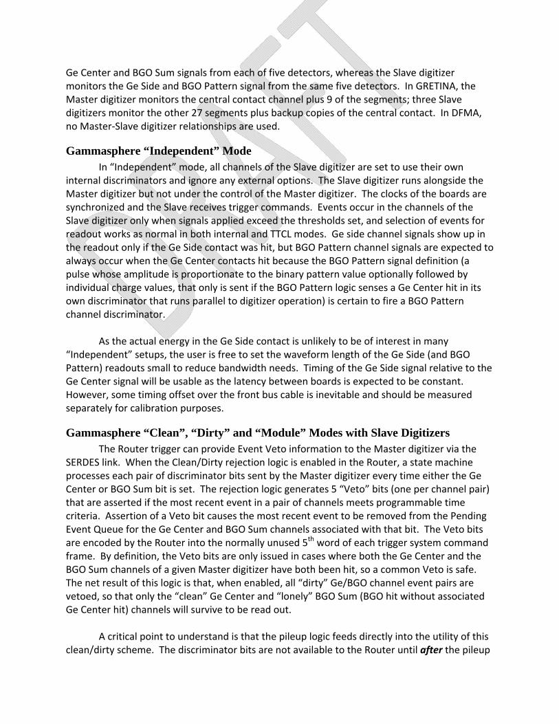
Ge Center and BGO Sum signals from each of five detectors, whereas the Slave digitizer monitors the Ge Side and BGO Pattern signal from the same five detectors. In GRETINA, the Master digitizer monitors the central contact channel plus 9 of the segments; three Slave digitizers monitor the other 27 segments plus backup copies of the central contact. In DFMA, no Master‐Slave digitizer relationships are used.
Gammasphere “Independent” Mode In “Independent” mode, all channels of the Slave digitizer are set to use their own internal discriminators and ignore any external options. The Slave digitizer runs alongside the Master digitizer but not under the control of the Master digitizer. The clocks of the boards are synchronized and the Slave receives trigger commands. Events occur in the channels of the Slave digitizer only when signals applied exceed the thresholds set, and selection of events for readout works as normal in both internal and TTCL modes. Ge side channel signals show up in the readout only if the Ge Side contact was hit, but BGO Pattern channel signals are expected to always occur when the Ge Center contacts hit because the BGO Pattern signal definition (a pulse whose amplitude is proportionate to the binary pattern value optionally followed by individual charge values, that only is sent if the BGO Pattern logic senses a Ge Center hit in its own discriminator that runs parallel to digitizer operation) is certain to fire a BGO Pattern channel discriminator. As the actual energy in the Ge Side contact is unlikely to be of interest in many “Independent” setups, the user is free to set the waveform length of the Ge Side (and BGO Pattern) readouts small to reduce bandwidth needs. Timing of the Ge Side signal relative to the Ge Center signal will be usable as the latency between boards is expected to be constant. However, some timing offset over the front bus cable is inevitable and should be measured separately for calibration purposes.
Gammasphere “Clean”, “Dirty” and “Module” Modes with Slave Digitizers The Router trigger can provide Event Veto information to the Master digitizer via the SERDES link. When the Clean/Dirty rejection logic is enabled in the Router, a state machine processes each pair of discriminator bits sent by the Master digitizer every time either the Ge Center or BGO Sum bit is set. The rejection logic generates 5 “Veto” bits (one per channel pair) that are asserted if the most recent event in a pair of channels meets programmable time criteria. Assertion of a Veto bit causes the most recent event to be removed from the Pending Event Queue for the Ge Center and BGO Sum channels associated with that bit. The Veto bits are encoded by the Router into the normally unused 5th word of each trigger system command frame. By definition, the Veto bits are only issued in cases where both the Ge Center and the BGO Sum channels of a given Master digitizer have both been hit, so a common Veto is safe. The net result of this logic is that, when enabled, all “dirty” Ge/BGO channel event pairs are vetoed, so that only the “clean” Ge Center and “lonely” BGO Sum (BGO hit without associated Ge Center hit) channels will survive to be read out. A critical point to understand is that the pileup logic feeds directly into the utility of this clean/dirty scheme. The discriminator bits are not available to the Router until after the pileup

time (“m”+”k”) has elapsed. Thus it is imperative that “m” and “k” be set to identically the same values in both the Ge Center and BGO Sum channels for a given detector or the clean/dirty logic cannot function. The cogent reader may also query whether pileup will affect whether the correct event can be selected to be vetoed. The answer to this is that the Pending Event Queue only contains Accepted events, not Extended events. This has two ramifications:
1) Since the PEQ only holds the timestamps of Accepted hits, a successful veto of one entry in the PEQ will by definition also veto any arbitrary number of following Extended events caused by pileup.
2) The only way to absolutely guarantee that accidental overlap of discriminator hits in pileup conditions does not create false excess vetoes is to run the discriminator in pileup‐reject mode.
This veto logic works irrespective of whether the digitizer is in “internal” or “TTCL”
mode. If using internal trigger the digitizers and routers will in the background strip out the dirty channel pairs by themselves. Additional event filtering may be implemented using the master trigger to sub‐select events based upon multiplicity and/or coincidence with other detectors. When using clean/dirty vetoes in the Router trigger, the Router may be set to report raw multiplicity, clean‐only multiplicity or lone‐BGO multiplicity to the Master trigger in either the “X” or “Y” sums. This allows for highly filtered readouts such as only the clean Ge Center channels that participated in a clean multiplicity greater than some threshold.
Effects of Vetoes within the Slave Digitizer
By virtue of the front bus cable the Slave digitizer receives the same Veto signals that the Master digitizer does. The Ge Side channels of the Slave digitizer are enabled to process vetoes but the BGO Pattern signals are not. This means that when the Veto is issued for a particular detector by the Router trigger, the Ge Center, BGO Sum and Ge Side channels will be vetoed but the BGO Pattern signals are not. By implementing the Slave logic this way none of the BGO Pattern data of triggered events is ever lost, allowing offline software to reconstruct the scatter pattern and later reject those events where neighboring BGO panels are both hit (the “electric honeycomb”).
Use of External Discriminator modes with “clean/dirty” vetoes in a Slave digitizer
In many cases a “dirty” event will fire the Ge Center discriminator but not the Ge Side channel due to drift direction. This leaves the previous event in the Ge Side channel, if not yet read out, at risk of being incorrectly vetoed. Thus, in high rate events, it is important to insure that the Ge Side channel always has a discriminator firing each time the Ge Center does. This may be accomplished by setting the External Discriminator mode of the Ge Side channels to “OR” mode, if the Master digitizer is also capable of sending all five Ge Center bits to the Slave. This can be done by overloading the 5th word of each command frame as only five bits of the sixteen available are used by the Veto signals. If the Ge Side has already fired of its own accord, the copied Ge Center will come soon enough that it will be swallowed by the discriminator holdoff logic. If the Ge Side hasn’t fired, the copied Ge Center forces an event to protect the integrity of the Pending Event Queue.

“Pseudo-GRETINA” Mode In “Pseudo‐GRETINA” mode, the Slave digitizer is in complete thrall to the operation of one channel of the Master digitizer. The discriminator bit from the one channel of the Master is sent on bit 17 of the front bus cable and all channels of the Slave digitizer are set to fire only when the external signal is asserted, using the External Discriminator option built into all ANL digitizer firmware. Thus, if the Master digitizer is set so that channels 1‐9 fire only from the external signal and the external signal is set to channel 0, channels 1‐9 are slaved to channel 0 and always sample whenever channel 0 fires. Similarly, in the Slave digitzer, all channels are set to use the external signal only and the external signal is set to be the copy of the discriminator bit from the Master digitizer’s channel 0. This then forces all channels in both boards to capture an event every time channel 0 of the Master digitizer fires, just like GRETINA. The exact same trigger acceptance messages received by the Master digitizer are received by the Slave digitizer, so all channels in the slave will read out the same events that come from the Master whether in internal or TTCL mode. Propagation delay across the front bus cable will be small so the same time windows are used in both digitizers for TTCL mode. Obviously, delay chain parameters ‘m’, ‘k’, ‘d’ and ‘d3’ must be set the same in all channels of both Master and Slave digitizers.

Technical Details of Channel Pipeline Operation This section provides greater technical detail on the operation of the channel delay pipeline, specifically focusing upon how internal timing operations are performed including pileup recognition and peak detection. The details of structure of the ANL digitizer channel are quite different from those of the LBNL firmware in that all internal timing is controlled using bits in the delay buffers rather than separate counters or timers. This greatly reduces the amount of logic required per channel and thus eases fitting of the design within the FPGA.
Memory Structures within Xilinx FPGAs The Xilinx FPGA implements two forms of memory resources, the Block RAM and Distributed RAM. All RAM within a Xilinx FPGA is dual‐port in nature. Block RAMs are 18kbit units that may be reconfigured into a few standard sizes (1Kx18, 512x36, etc.). The bit‐width of all Block RAM implementations is based upon a parity memory so that there are always a multiple of nine, rather than eight, bits of width. Most of the time these extra bits are ignored but as they are inherent to the Block RAM architecture they may be used to carry data unrelated to the other bits so long as common clocking is acceptable. On the down side, Block RAM is scattered throughout the chip in fixed areas so as more and more of the Block RAM is used, it becomes increasingly difficult to route signals to those Block RAMs that remain. Many designs fail to route not because the chip is full, but because the design tries to use every Block RAM and the router software cannot find paths to every RAM at the speed required. Distributed RAM memory uses the actual memory of the many logic slices of the FPGA itself. Every logic slice within the FPGA implements small 16x1 memories to perform the basic logic functions (AND, OR, etc.) as it is more efficient to simply use a small lookup table than to implement hard gates. This distributed RAM may be ganged together in small units to replace Block RAM and has the placement advantage of always being physically near the logic that wants to use it. Additionally, unlike block ram, the width of distributed structures is arbitrary. The downside of distributed RAM is that it requires some logic to gang together so sizes above 128x16 are usually impractical. When implementing a delay structure as opposed to a general‐purpose dual‐port memory, the Distributed RAM may be further optimized through the use of specific shift register macros named “SRL” in the Xilinx literature. These SRL macros use special internal connections available within the 16X1 distributed RAM buffer to “rewire” the RAM into a 16‐element shift register. Data enters at position 0 and any one position may be brought out as the output. Serially ganging these SRLs together – assuming interconnect delays between them can meet timing constraints – allows arbitrarily long delay buffers to be implemented. As the SRL method does not require the address counters necessary in a generic dual‐port RAM implementation, the SRL methodology provides very significant resource utilization reductions. In the digitizer module, the actual ADC data is only 14 bits wide; thus, if we use a mix of 18‐bit wide Distributed RAMs along with 1Kx18 Block RAMs, there are four bits available for timing purposes across the entire delay chain. As most timing parameters are associated with

the buffer lengths use of these extra bits to form state machine delays is highly efficient. The normal method by which this is done is to have a state machine generate a pulsed signal one clock period wide at the start of a delay state that is connected to the input side of a delay buffer. The state machine then waits for the delayed copy of the bit to fall out of the other side of the delay buffer before proceeding or branching. Resources needed to implement a delay counter are eliminated and comparison logic is reduced to a single bit. While this may not seem like much, multiply over 10 channels with multiple delays per channel and a significant fraction of the FPGA’s resources are conserved.
Delay Structures within the Channel Logic Many delay structures have been implemented in the channel logic as shown in Figure 19. Each of these is explained in detail below.
Figure 19 ‐ Timing model of the channel logic
Chain Validity Logic (system initialization) Whenever the user modifies the timing parameters of the channel, typically by changing the delay values, the ADC data in the chain immediately becomes invalid. After changes to timing parameters have been loaded, in response to the user setting the “load delays” bit in a master control register, the signal CHAIN_INVALID is asserted and a pulse named CHAIN_INVALID_PULSE enters the channel delay chain. Only after the pulse has propagated
PILEUP TIMING
BASELINE TRACKINGCFD CONTROL
DISCRIMINATORSAMPLING BUFFER
DISCRIMINATORBIT FORMATIONCOMPENSATION PRE-RISE DELAY
MAX DEPTH = 128(kval, 6:0)
MAX DEPTH = 128(dval, 6:0) FIXED DEPTH = 18
RISE BEFOREDISCRIMINATORFIRING DELAY
MAX DEPTH = 32(d3val, 4:0)
13..0
ADCRECODE 13..0
DelayP1 13..0
DelayP2 13..0
DelayM1 13..0
DelayK 13..0
DelayD 13..0
DelayD2 13..0
DelayD3 13..0
DelayM2 13..0
Trig Dly1 13..0
Trig Dly2 ADC_OUT
POST-RISE DELAYRISE TIME
REMAINDER
CoarseDisc.
TO FRONTPANEL
DelayP2
DelayM1
DelayK
DelayD
DelayD2
DelayD3
DelayM2
Trig Dly1
Trig Dly2
DelayM1
DelayK
DelayD3
DelayM2
Trig Dly1
Trig Dly2
DelayM1
DelayK
Trig Dly1
Trig Dly2
DelayD
DelayP114
CHAIN_INVALID_PULSE
16
17
14
16
14
16
14
17
14
15
14
15
14
15
16
14
15
16
14
15
16
17
14
17
14CHAIN_VALID_PULSE
THRESH_DISC_FLAG
CHAIN_INVALID
DISCBIT_PILEUP_RELEASE
17ENERGY_INVALID
PEAK_FLAG_MARKER_DELAYED
15
CFD_PK_FLG_MARKER
DelayK19
THRESH_DISC_FLAG
19
CFD_PRE_TRIGGER
18 DelayD
PEAK_FLAG_MARKER18
15
DISCBIT_HOLDOFF_RELEASE
17DISCBIT_HOLDOFF_RELEASED_DLYD
DelayD16
THRESH_DISC_FLAG
16THRESH_DISC_FLAG_DLYD
INTERNAL_TIMING_MARK
INT_ACCEPTED_HIT
TRIGGER DELAY TRIGGER DELAY
MAX DEPTH = 1024 (mval, 9:0) FIXED DEPTH = 1024 FIXED DEPTH = 1024
MAX DEPTH = 1024 (mval, 9:0)
TIMING_MARK
EVENT_EXPIREDWAVEFORM READOUT
Trig Dly1
Trig Dly2
17 17
17
BASELINE_DELAY_FLAG_IN BASELINE_DELAY_FLAG_OUT
17BASELINE_TRACK_DLY_IN BASELINE_TRACK_DLY_OUT
SYSTEM INITIALIZATION
Accum. Accum.
DelayD
Leading-EdgeDiscriminator

the entire length of the chain – when CHAIN_VALID_PULSE comes out – may the discriminator or any other measurement be performed. This logic insures that no false events or partial events propagate to the readout when operational parameters are modified. Similarly, energy calculations are delayed further, by the length of the summation buffers “M1” and “M2”, to insure that the accumulators that calculate the pre‐ and post‐rise energy are not considered valid until a full new set of ADC samples have been processed after the chain has become valid.
Waveform Readout Timing marks for discriminator, hold‐off and peak detection are inserted into the waveform data at the input to the “d3” buffer, so that they are aligned to the actual waveform samples in which the marks of interest occurred. As the definitions of the marks change dependent upon the discriminator mode, excess bits in the “d” and “k” buffers are used to re‐align the peak detection timing mark as required. Similarly, as the pileup logic is calculated relative to the discriminator, the result of the pileup logic is re‐inserted into the delay chain at the entry into the trigger timing delay so that the readout logic is advised when events have expired and can no longer be read out by the same trigger delay.
CFD timing control The constant‐fraction discriminator is enabled by the leading‐edge discriminator. As the leading‐edge logic has different alignment relative to its buffer edges than does the CFD, a delay equal to the delay being used by the leading‐edge discriminator in CFD mode is used to properly time CFD operation. Similarly, when the user has selected the “external discriminator ‐ OR” mode of operation, a differently delayed copy of the leading‐edge discriminator result is used to properly time operation in that mode.
Pileup timing As the pileup time is defined by the user parameters, use of an extra bit in the same delay buffers as are used for the ADC data ensures that the pileup logic is always timed correctly. Internal checking logic to determine if the user has inadvertently set the pileup time less than the hold‐off time is similarly self‐timed by using another bit in the “d” buffer.
Diagnostic capabilities using the on-board DAC The global DAC multiplexer implemented for board‐wide diagnostics allows a selected waveform from any of the 10 channels to be driven out the front panel DAC output. Each channel has a separate diagnostic waveform selection multiplexer that allows one of four diagnostic waveforms to be selected.
Selection “00” copies the raw ADC data at the output of the P2 buffer of the channel to the DAC, for direct monitoring of input signals.
Selection “01” generates a digital‐like signal that shows, in time, when the baseline tracking logic is active.
Selection “10” monitors the ADC data as it is entering the buffer used by the leading‐edge discriminator.

Selection “11” monitors the baseline tracker by driving the DAC with the slowly tracking baseline value itself (BASE_SAMPLE), so that the slew rate and filtering characteristics of the baseline logic may be viewed directly.
A suggested procedure at system startup is to monitor the baseline of a channel using
an oscilloscope with no beam present but all electronics on. Reset the baseline logic of the channel. The signal should ‘home’ to the user‐supplied estimated baseline and then begin tracking. Tracking will continue until the leading edge discriminator fires. For low event rates one should see the baseline hold steady during events but re‐track between events.
Accuracy and Pole-Zero considerations High event rates can introduce pole‐zero errors, as the pre‐rise buffer no longer sums over an assumed flat region, but is riding upon the exponential decay of the previous pulse. In an effort to provide additional data to allow for offline correction of these issues, the ANL firmware generates the following data values in the header:
The Pre‐rise enter sample and Pre‐rise leave sample are the single ADC data points at the beginning and end of the pre‐rise buffer sampled when the discriminator fired.
The Post‐rise sample is the single ADC data point at the beginning of the post‐rise buffer sampled when the discriminator fired.
The Base Sample value is a sample of the maximally filtered running baseline calculation, captured at the time the discriminator fired.
The Sampled baseline differs from the Base Sample in that it is the current running sum of presumed baseline samples across the 10.24usec buffer; as such it is less filtered than the Base Sample.
The Peak Sample value is the single ADC data sample entering the pre‐rise buffer at the moment the peak detector logic has fired; this is intended to provide an amplitude value to go along with the time value Timestamp of Peak detect.
The Timestamp of Previous Discriminator is latched every time the discriminator fires and provides the time differential between the time of the event being read out and the previous discriminator firing, even if that event was not read out.
The Last Post‐Rise enter and Last Post‐Rise leave Samples are the two ADC samples at beginning and end of the post‐rise buffer saved from the previous discriminator firing.
The post‐rise samples from the previous event and the pre‐rise samples from the current event provide four data points that can be fit to an exponential decay, if the decay characteristics of the detector signal are known. This is shown in Figure 20.

Figure 20 ‐ Correction of current event from data passed forward from the previous event.
As the timestamp of the current event and the timestamp of the previous event are saved in the header (even if the previous event did not read out due to trigger or pileup settings), the exact time of the two post‐rise ADC samples from the previous event can be determined from the delay buffer values. Referring to Figure 3, where the digitizer is in leading‐edge mode, the two samples at either end of the post‐rise buffer occur at [TS(event) + “k”] and [TS(event) + “k” + “m”], respectively, relative to their discriminator firing. Thus, the post‐rise samples from the previous event must occur at times [TS(previous event) + “k”] and [TS(previous event) + “k” + “m”]. Using the same method, the times of the two samples spanning the pre‐rise buffer are given as [TS(event) ‐ “d” ‐ “d2” ‐ “d3”] and [TS(event) ‐ “d” ‐ “d2” ‐ “d3” ‐ “m”], respectively. The exponential fit may then be made by offsetting all times by subtracting [TS(previous event) + “k” ‐ 1], such that for purposes of fitting the four ADC samples occur at relative times
1,
“m”+1
[TS(event) ‐ TS(previous event) ‐ “k” ‐ “d” ‐ “d2” ‐ “d3” ‐ “m” + 1] and
[TS(event) ‐ TS(previous event) ‐ “k” ‐ “d” ‐ “d2” ‐ “d3” + 1]
Once offset these times may be converted to natural logarithms of times (hence the +1, to avoid ln(0) issues) and fit as four (amplitude, ln(time)) numbers using the standard linear regression technique, using the ADC value of the eldest sample minus the baseline as the starting amplitude of the exponential decay. This will provide the time constant, assuming a single dominant exponential decay, allowing for pole‐zero correction of both the pre‐rise

and post‐rise sums of the current event. As the delta‐time between the pre‐rise and post‐rise sums is also known from “k”, “d”, “d2” and “d3”, the user may elect to extend the fitted curve to span both sums and apply separate corrections to each. Additional information may be gleaned by using the SAMPLED_BASELINE value of the header. This 24‐bit value is the sum of all the ADC values contained within the T1 buffer, spanning the time range [TS(event) ‐ “d” ‐ “d2” ‐ “d3” ‐ “m”] to [TS(event) ‐ “d” ‐ “d2” ‐ “d3” ‐ “m” ‐ 10.24us]. If the previous discriminator firing is sufficiently far back in time such that this sum is not corrupted by the previous event, this value can be used to estimate a 5th data point for the exponential fit. This excess “ADC sample” would be the SAMPLED_BASELINE value, divided by 1024, at time [TS(event) ‐ “d” ‐ “d2” ‐ “d3” ‐ “m” ‐ 5.12us]. Comparing the sum of fitted curve values over the time range of SAMPLED_BASELINE against SAMPLED_BASELINE may also be considered as a “sanity check” of the curve fitting process.
Time interpolation using the CFD Sample values The three CFD Sample values provided in the CFD‐mode header allow interpolation of the timestamp. The CFD equation [X(n) * fraction] – X(n‐d) for a positive‐going pulse is expected to rise and then plummet through zero to a negative value as the input passes the fractional percentage value desired. The CFD logic samples the timestamp at the moment the sign of the CFD equation changes. The CFD Sample values are the values of the CFD equation at the clock tick when the timestamp is latched, the sample one clock tick earlier and the sample two clock ticks earlier. Thus, the expectation is that there will be two positive and one negative samples captured for a positive‐going input pulse. These three values are simply entered into a linear regression and the intercept (where the fit line equals zero) determined. The non‐zero fractional ‘x’, or time, value at Y=0 is subtracted from the timestamp reported to obtain the interpolated timestamp. The accuracy of the interpolation method is highly dependent upon the rise time of the incoming signal, and secondarily dependent upon the amplitude of the incoming signal. This is simply because the CFD timing accuracy is proportionate to the slope of the effective differentiator, so faster rising inputs yield a greater slope and thus less time (x) error. At small signal/noise ratios the fit gets “fuzzy”. Typical results obtained using signals with 800‐1000ns rise times are a 1‐sigma normal distribution of interpolated time results of about 1.7ns for relatively large signals, degrading to a 1‐sigma of about 2.5ns for tiny signals at the limits of leading edge discriminator detection.