analysis of reliability for fault tolerant design in nano ... · a fault tolerant design is applied...
TRANSCRIPT
Journal of Experimental and Theoretical Nanotechnology Specialized Researches (JETNSR) VOL: 2, NO 1, 2018
SIATS Journals
Journal of Experimental &Theoretical Nanotechnology Specialized Researches
(JETNSR)
Journal home page: http://www.siats.co.uk
Journal of Experimental and Theoretical Nanotechnology Specialized Researches
Analysis of Reliability for Fault Tolerant Design in NANO CMOS Logic Circuit
2, Pradipkumar Dixit1D.Manimekalai
Engineering, Jain University, Research Scholar, Department of Electrical and Electronics 1
Bangalore, India. 2Professor, Department of Electrical and Electronics Engineering, M .S. Ramaiah Institute of Technology,
Bangalore, India Email: [email protected]
A R T I C L E I N F O Article history:
Received 27 March 2016, Revised 29 May 2016, Accepted 11 July 2016 Available online 15 Jan 2018
Keywords: Nano CMOS; Fault; Reliability. PACS: 85.35-p; 91.55Jk; 88.50gj.
Journal of Experimental and Theoretical Nanotechnology Specialized Researches (JETNSR) VOL: 2, NO 1, 2018
61
Journal of Experimental and Theoretical Nanotechnology Specialized Researches
Abstract
The emerging nano scaled electronic devices are Carbon Nanotubes (CNT), Silicon nanowires (SINW), nano CMOS switches etc. In Nano CMOS switches, the devices can be interconnected to build the nano scaled CMOS circuit. In this nano CMOS circuit, faults occur at three levels, such as gate level, circuit level and switch level. This paper focusses on the switch level faults of stuck-open or stuck-off and stuck-short or stuck-on that frequently occurs in CMOS switches. To overcome the switch level faults and to increase the reliability, the fault tolerant technique known as the Quadded Transistor (QT) structure is used. An analytical model has been formulated to determine the probability of failure by analyzing the stuck open and stuck short faults. Also, the model has been formulated by implementing QT structure for the single CMOS NAND2 gate. By the use of analytical formulations, the results has been simulated for the occurrence of minimum to maximum number of defective transistors in CMOS logic circuit.
Journal of Experimental and Theoretical Nanotechnology Specialized Researches (JETNSR) VOL: 2, NO 1, 2018
61
Journal of Experimental and Theoretical Nanotechnology Specialized Researches
1. . Introduction
Recent advances in CMOS Scaling technology has reduced the SiO2 layer thickness below 2nm. The major causes for the reduction in oxide layer thickness include increase in gate leakage currents, increase in poly-silicon gate depletion, gate dopant penetration into the channel, reliability issues and stand by power consumption [1]. When the transition of CMOS technology changes from one generation to the next, the channel doping concentration is increased and the SiO2 layer thickness is reduced which results in reduction in gate channel length. A large number of variations in different parameters of the MOSFET have been tried to enhance the performance. From that, the most prominent parameter variation is the reduction of gate channel length in the nanometer regime [2]. When the scaling of CMOS devices enters nanometer regime, there exist higher manufacturing defect rates in the order of 10-1 to 10-3 units which has lower reliability [3]. The reliability issues in nano scaled CMOS devices can be sequentially classified as defects, faults, error and failure. This occurs due to environmental factors such as temperature, humidity, electric field etc. In general, a defect is defined as any physical imperfection which does not satisfy specified requirements. A fault is a critical defect which affects the functional performance of the circuit. An error is a manifestation of a fault. A failure is an event i.e inoperable state due to the occurrence of defect, fault and error.
Natasa Miskov [4] has defined the kinds of faults as permanent, transient and intermittent faults. Permanent faults remain stable until a repair or replacement is undertaken. Transient faults occur for a short period of time. Intermittent faults occur first which eventually tends to be permanent. The fault tolerant design methodologies are essentially required for any nano scaled system/circuit to improve the reliability. This can be achieved by introducing redundancy [5]. There are three forms of redundancies namely time, information and space. In time redundancy computations are repeated during specific period of time. In information redundancy, the number of bit errors in a data can be detected, coded and, corrected by the use of error-detection and error-correction codes [6]. Finally, space redundancy is normally based on the number of devices or gate combinations arranged in a system. This space redundancy usually developed at three different levels in the digital system such as circuit, gate and transistor level redundancy.
The circuit level redundant technique [7] namely Triple Modular Redundancy (TMR) can be widely used in mission-critical applications where system safety and reliability is essential. The TMR triplicates the circuit/system and the outputs of the three modules are voted through a majority voter. Thus, TMR technique can tolerate any single defect or fault that occur in one of the triplicated modules of circuit/system. Tejinder singh et. al [8] used the Triple Modular Redundancy (TMR) to tolerate the manufacturing defects. They designed and analysed the 4-bit Arithmetic and Logic unit (ALU) circuit using CMOS 180nm process technology for fault tolerant computing structures, that estimates the power consumption which results for all the arithmetic and logical operations.
Journal of Experimental and Theoretical Nanotechnology Specialized Researches (JETNSR) VOL: 2, NO 1, 2018
61
Journal of Experimental and Theoretical Nanotechnology Specialized Researches
M.Stanisavljevic et.al [9-11] has analysed the gate level redundancy for the performance of the circuit in terms of reliability. They derived the optimal size of redundant units (number of chips) for several gate level fault-tolerant techniques such as R-Fold Modualar Redundancy (RMR), Cascaded RMR, Distributed R-fold Modular Redundancy (DRMR) etc . Walid Ibrahim et. al [12] developed a Bayesian based EDA tool called GREDA that estimates the accurate reliability of any CMOS gate. This tool considers the gate’s topology, the input vectors, reliability of the individual devices and noise margins to calculate the Gate Failure Probability (PFgate) more accurately. They also proposed [13] the optimum sizing method to optimize the trade-off between reliability and the power–area–delay parameters with several transistor sizing options. They have shown the improvement of the reliabilities in terms of factors of INV as 105, NAND2 as 10 and NOR-2 as 1010 .
The transistor level redundancy are introduced by adding transistors in the CMOS logic circuit. Some of the transistor level redundant techniques are Quadded Transistor Structure, Stacking Technique etc [14]. Jie Han et.al [15] proposed a novel fault tolerant technique known as Quadded Logic Quadded Transistor (QLQT) technique. In this technique, Quadded Transistor (QT) is implemented at the output layer of the circuit, while Quadded Logic (QL) is implemented for the circuit other than the output layer. The errors in the output layers of a circuit cannot be corrected by QL, but QT’s can correct the errors at the last two output layers. They evaluated the QLQT technique using stochastic computational models and proved that the QLQT technique performs the best in terms of reliability compared to other fault tolerant techniques such as triple modular redundancy (TMR) and triple interwoven redundancy (TIR).
A.H.Elmaleh et.al [16] has analysed a defect tolerant technique Quadded Transistor (QT) Structure for tolerating the transistor level defects such as stuck-open, stuck-short and bridging defects. They demonstrated the experimental results for ISCAS benchmark circuits by implementing the QT technique. This provides less circuit failure probability and high defect tolerance. Also they compared the results with other techniques such as Quadded Logic at the gate level and TMR at the unit level. Philip Schiefer et. al [17] used Quadded Logic Cell (QLC) structure as a fault tolerant technique for stuck-at faults. They proposed the dual transistor redundant NAND GATE for performing a comparative assessment of the stuck-at fault resilence for the non-redundant and redundant NAND gate. The simulation results for Stuck-at High (SAH) and Stuck- at Low (SAL) faults for redundant NAND gate shows that the fault rate falls to 8.3% in comparison to the 25% for non-redundant gate. It has been proved that this transistor level redundancy have higher fault tolerance than the redundancy at the circuit or gate level.
This paper investigates two types of switch level faults namely stuck-open and stuck-short that frequently occurs in CMOS switches. A fault tolerant design is applied for CMOS logic circuit by adding transistor level redundancy to improve the reliability of the CMOS logic circuit. The objectives of this paper are stated as follows:
Journal of Experimental and Theoretical Nanotechnology Specialized Researches (JETNSR) VOL: 2, NO 1, 2018
61
Journal of Experimental and Theoretical Nanotechnology Specialized Researches
To increase the transistor level redundancy that tolerates permanent faults of stuck- open and stuck-short for CMOS NAND2 logic circuit.
To tolerate the stuck-open and stuck-short faults, the Quadded Transistor (QT) Structure should be used to improve the reliability.
The circuit failure probability should be measured by the reliability of CMOS NAND2 logic circuit by considering various factors such as the input vectors, the transistor type and the transistor’s topology.
The analysis of the reliability and the fault tolerance level of NAND2 logic circuit should be determined through several simulation runs using circuit failure probability of CMOS NAND2 logic circuit.
This paper is organized as follows. In section 2, the analysis of stuck-open and stuck-short faults are described with the fault tolerant technique. Also the analytical formulation are modelled to determine the circuit failure probability of a CMOS NAND2 gate. In section 3, the proposed NAND2 circuit is configured, followed by the application of analytical model to analyse reliability and fault tolerance. In section 4, simulation results are discussed. Finally, the conclusion is given in section 5.
2. Development of Analytical Model for Fault Tolerance and Reliability Improvement 2.1 Stuck-open and Stuck-short faults In this paper, we analyzed the transistor level permanent faults such as stuck-open and
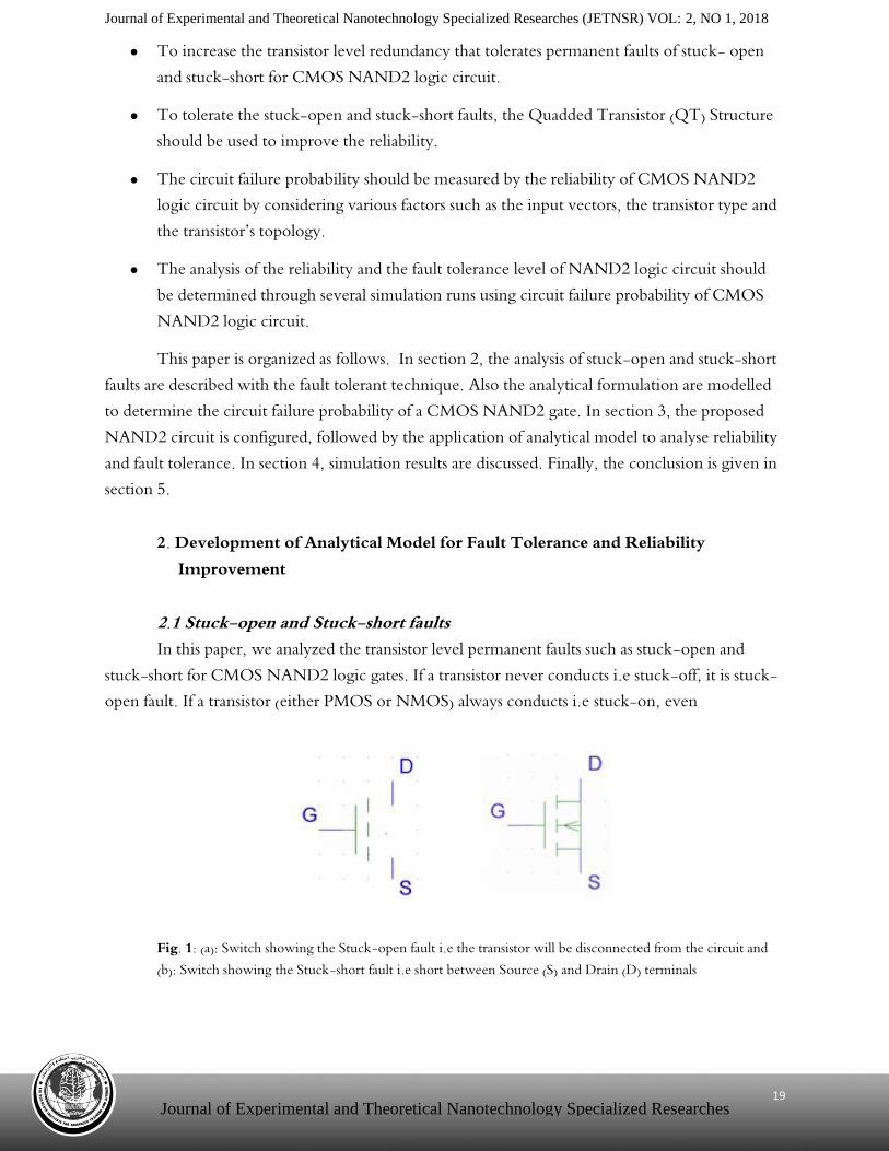
stuck-short for CMOS NAND2 logic gates. If a transistor never conducts i.e stuck-off, it is stuck- open fault. If a transistor (either PMOS or NMOS) always conducts i.e stuck-on, even
Fig. 1: (a): Switch showing the Stuck-open fault i.e the transistor will be disconnected from the circuit and (b): Switch showing the Stuck-short fault i.e short between Source (S) and Drain (D) terminals
Journal of Experimental and Theoretical Nanotechnology Specialized Researches (JETNSR) VOL: 2, NO 1, 2018
02
Journal of Experimental and Theoretical Nanotechnology Specialized Researches
when the input is not given, it is stuck-short fault. Stuck-open or stuck off faults can be emulated by disconnecting the transistor from the circuit as shown in Fig.1 (a) which means connecting the gate (G) terminal to a logic 0 for NMOS transistor and logic 1 for PMOS transistor. Stuck-short faults can be emulated by a short between the source (S) and drain (D) terminals of the transistor is shown in Fig.1 (b) So that, the gate terminal of the transistor will be disconnected and it will be directly connected to logic 1 for NMOS transistor or logic 0 for PMOS transistor.
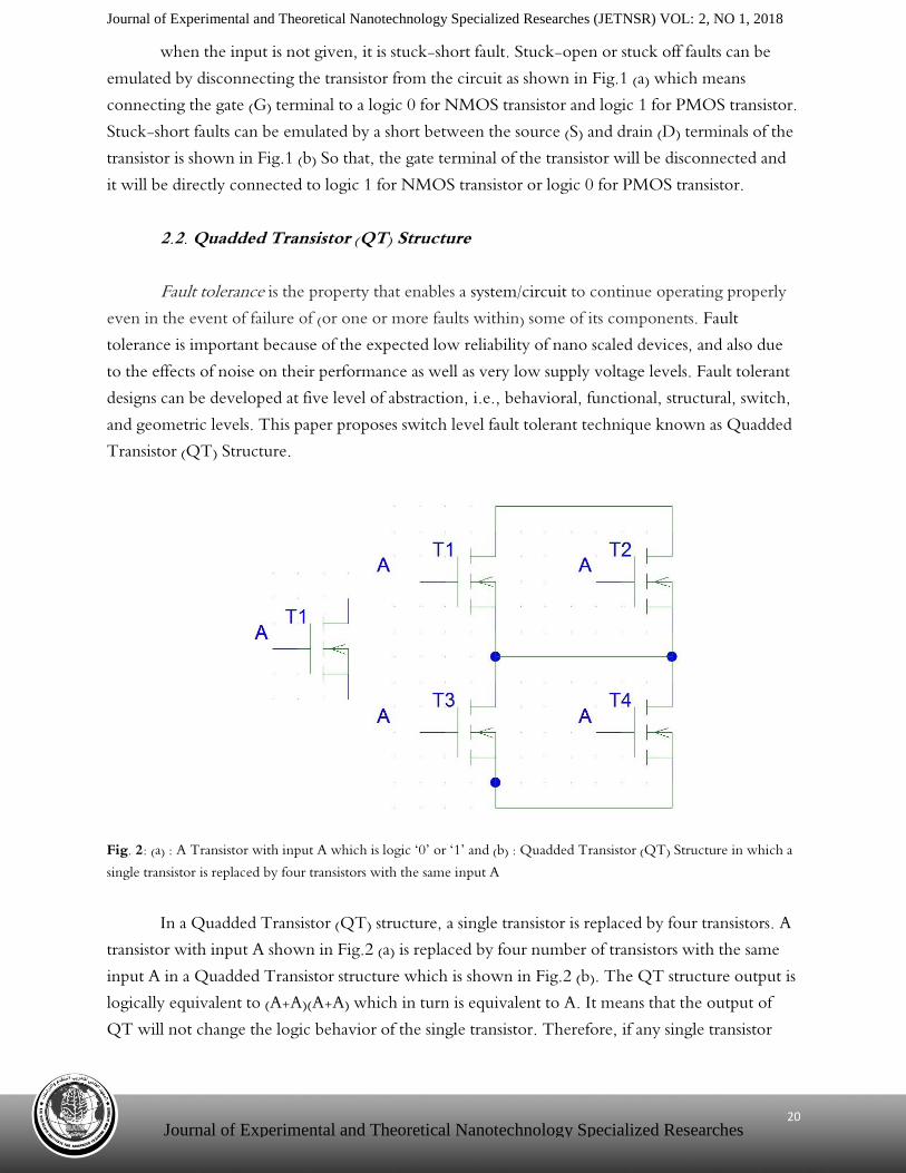
2.2. Quadded Transistor (QT) Structure
Fault tolerance is the property that enables a system/circuit to continue operating properly even in the event of failure of (or one or more faults within) some of its components. Fault tolerance is important because of the expected low reliability of nano scaled devices, and also due to the effects of noise on their performance as well as very low supply voltage levels. Fault tolerant designs can be developed at five level of abstraction, i.e., behavioral, functional, structural, switch, and geometric levels. This paper proposes switch level fault tolerant technique known as Quadded Transistor (QT) Structure.
Fig. 2: (a) : A Transistor with input A which is logic ‘0’ or ‘1’ and (b) : Quadded Transistor (QT) Structure in which a single transistor is replaced by four transistors with the same input A
In a Quadded Transistor (QT) structure, a single transistor is replaced by four transistors. A transistor with input A shown in Fig.2 (a) is replaced by four number of transistors with the same input A in a Quadded Transistor structure which is shown in Fig.2 (b). The QT structure output is logically equivalent to (A+A)(A+A) which in turn is equivalent to A. It means that the output of QT will not change the logic behavior of the single transistor. Therefore, if any single transistor
Journal of Experimental and Theoretical Nanotechnology Specialized Researches (JETNSR) VOL: 2, NO 1, 2018
06
Journal of Experimental and Theoretical Nanotechnology Specialized Researches
fault (stuck-open or stuck-short) occur in QT structure, it can be tolerated by adding fault tolerant technique. Also, it should be observed that double stuck open faults can be tolerated as long as they do not occur in any two parallel transistors T1&T2 or T3&T4. Double stuck short faults can be tolerated as long as they do not occur in two series transistors T1&T3, T1&T4, T2&T3 or T2&T4. Thus, the fault tolerance could be improved by implementing this quadded transistor structure.
2.3 Proposed Analytical model
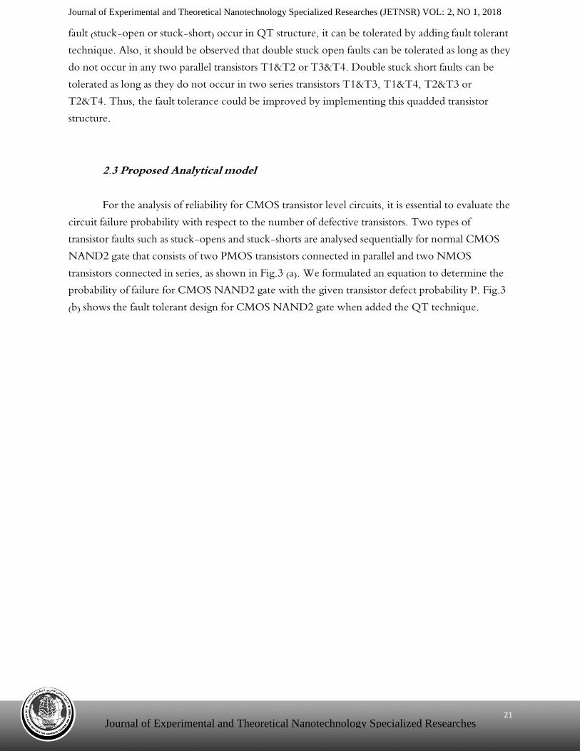
For the analysis of reliability for CMOS transistor level circuits, it is essential to evaluate the circuit failure probability with respect to the number of defective transistors. Two types of transistor faults such as stuck-opens and stuck-shorts are analysed sequentially for normal CMOS NAND2 gate that consists of two PMOS transistors connected in parallel and two NMOS transistors connected in series, as shown in Fig.3 (a). We formulated an equation to determine the probability of failure for CMOS NAND2 gate with the given transistor defect probability P. Fig.3 (b) shows the fault tolerant design for CMOS NAND2 gate when added the QT technique.
Journal of Experimental and Theoretical Nanotechnology Specialized Researches (JETNSR) VOL: 2, NO 1, 2018
00
Journal of Experimental and Theoretical Nanotechnology Specialized Researches
Fig. 3: (a): CMOS equivalent circuit of 2 input NAND Gate with two inputs A and B and (b): CMOS equivalent circuit of NAND2 Quadded Transistor Structure in which four transistors are replaced by four number of QT structures.
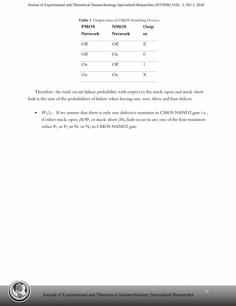
If stuck-open and stuck-short faults occur in NANO CMOS logic circuits, then there will be four states of output such as logic 0, logic 1, unknown X and floating Z as shown in Table 1. Both unknown X and floating Z outputs are considered as output errors which lead to failure of the circuit. This assumption has been taken to determine the circuit failure probability.
Journal of Experimental and Theoretical Nanotechnology Specialized Researches (JETNSR) VOL: 2, NO 1, 2018
02
Journal of Experimental and Theoretical Nanotechnology Specialized Researches
Table 1. Output states of CMOS Switching Devices.
PMOS Network
NMOS Network
Output
Off Off Z
Off On 0
On Off 1
On On X
Therefore, the total circuit failure probability with respect to the stuck-open and stuck-short
fault is the sum of the probabilities of failure when having one, two, three and four defects.
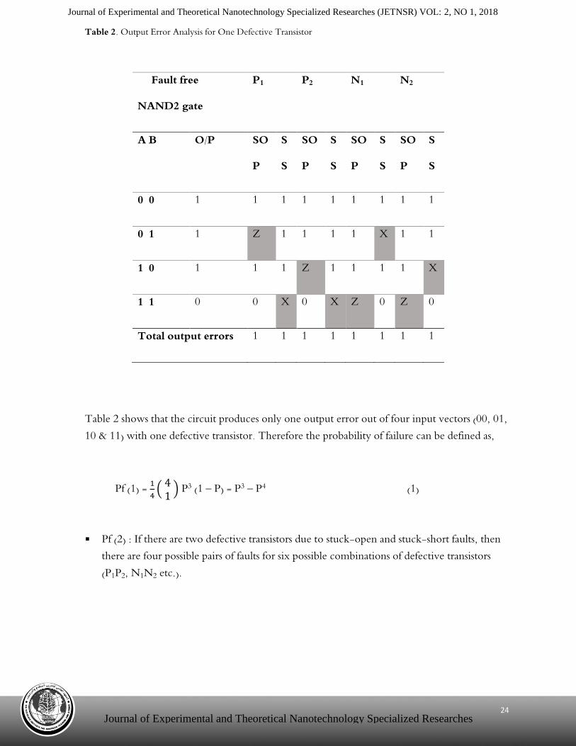
Pf (1) : If we assume that there is only one defective transistor in CMOS NAND2 gate i.e., if either stuck-open (SOP) or stuck-short (SS) fault occur in any one of the four transistors either P1 or P2 or N1 or N2 in CMOS NAND2 gate.
Journal of Experimental and Theoretical Nanotechnology Specialized Researches (JETNSR) VOL: 2, NO 1, 2018
02
Journal of Experimental and Theoretical Nanotechnology Specialized Researches
Table 2. Output Error Analysis for One Defective Transistor
Fault free
NAND2 gate
P1 P2 N1 N2
A B O/P SO
P
S
S
SO
P
S
S
SO
P
S
S
SO
P
S
S
0 0 1 1 1 1 1 1 1 1 1
0 1 1 Z 1 1 1 1 X 1 1
1 0 1 1 1 Z 1 1 1 1 X
1 1 0 0 X 0 X Z 0 Z 0
Total output errors 1 1 1 1 1 1 1 1
Table 2 shows that the circuit produces only one output error out of four input vectors (00, 01, 10 & 11) with one defective transistor. Therefore the probability of failure can be defined as,
Pf (1) = 14
( 41
) P3 (1 – P) = P3 – P4 (1)
Pf (2) : If there are two defective transistors due to stuck-open and stuck-short faults, then there are four possible pairs of faults for six possible combinations of defective transistors (P1P2, N1N2 etc.).
Journal of Experimental and Theoretical Nanotechnology Specialized Researches (JETNSR) VOL: 2, NO 1, 2018
02
Journal of Experimental and Theoretical Nanotechnology Specialized Researches
Table 3. Output Error Analysis for Two Defective Transistors
Fault free NAND2
gate
P1 P2 P1 N1
A B O/P P1 P2 O/P P1 N1 O/P
0 0 1 SOP SOP Z SOP SOP 1
SOP SS 1 SOP SS 1
SS SOP 1 SS SOP 1
SS SS 1 SS SS 1
0 1 1 SOP SOP Z SOP SOP Z
SOP SS 1 SOP SS 0
SS SOP 1 SS SOP 1
SS SS 1 SS SS Z
1 0 1 SOP SOP Z SOP SOP 1
SOP SS 1 SOP SS 1
SS SOP 1 SS SOP 1
SS SS 1 SS SS 1
1 1 0 SOP SOP 0 SOP SOP X
SOP SS X SOP SS 0
SS SOP X SS SOP 1
SS SS X SS SS Z
Total output errors 6 6
Journal of Experimental and Theoretical Nanotechnology Specialized Researches (JETNSR) VOL: 2, NO 1, 2018
01
Journal of Experimental and Theoretical Nanotechnology Specialized Researches
From the 6 possible combinations of two defective transistors, analysis of two combinations such as P1P2 and P1N1 are shown in Table 3. It shows that, out of 16 (4X4) possible combinations (4 for each input vector) , these stuck-short and stuck-open pairs of faults produces 6 output errors and therefore the probability of failure with two defective transistors can be defined as,
Pf (2) = 6
16(
42
) P2 (1 – P)2 = 9
4 P2 (1 – P)2 (2)
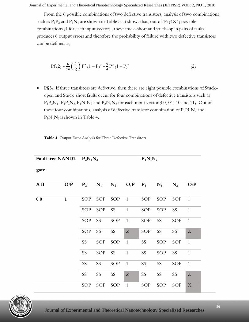
Pf(3): If three transistors are defective, then there are eight possible combinations of Stuck-open and Stuck-short faults occur for four combinations of defective transistors such as P1P2N1, P1P2N2, P1N1N2 and P2N1N2 for each input vector (00, 01, 10 and 11). Out of these four combinations, analysis of defective transistor combination of P2N1N2 and P1N1N2 is shown in Table 4.
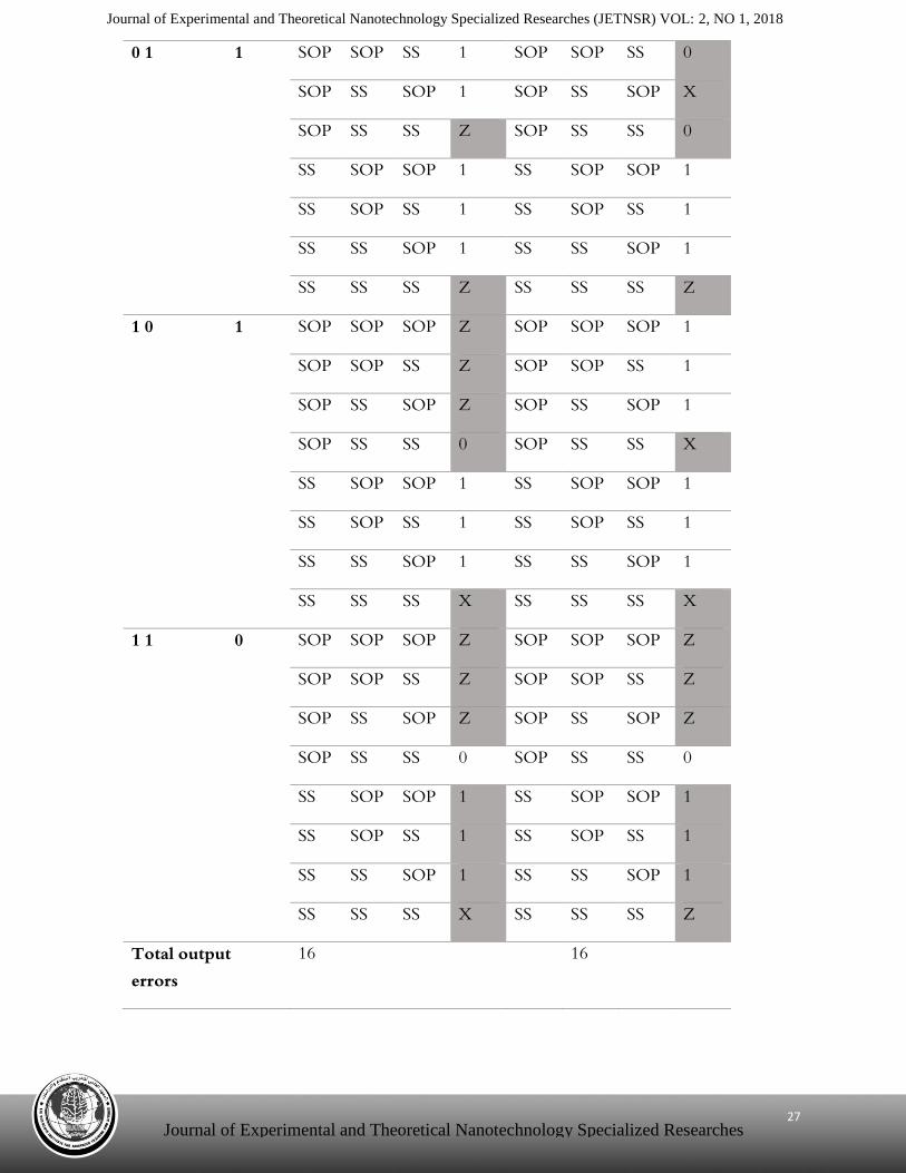
Table 4. Output Error Analysis for Three Defective Transistors
Fault free NAND2
gate
P2N1N2 P1N1N2
A B O/P P2 N1 N2 O/P P1 N1 N2 O/P
0 0 1 SOP SOP SOP 1 SOP SOP SOP 1
SOP SOP SS 1 SOP SOP SS 1
SOP SS SOP 1 SOP SS SOP 1
SOP SS SS Z SOP SS SS Z
SS SOP SOP 1 SS SOP SOP 1
SS SOP SS 1 SS SOP SS 1
SS SS SOP 1 SS SS SOP 1
SS SS SS Z SS SS SS Z
SOP SOP SOP 1 SOP SOP SOP X
Journal of Experimental and Theoretical Nanotechnology Specialized Researches (JETNSR) VOL: 2, NO 1, 2018
01
Journal of Experimental and Theoretical Nanotechnology Specialized Researches
0 1 1 SOP SOP SS 1 SOP SOP SS 0
SOP SS SOP 1 SOP SS SOP X
SOP SS SS Z SOP SS SS 0
SS SOP SOP 1 SS SOP SOP 1
SS SOP SS 1 SS SOP SS 1
SS SS SOP 1 SS SS SOP 1
SS SS SS Z SS SS SS Z
1 0 1 SOP SOP SOP Z SOP SOP SOP 1
SOP SOP SS Z SOP SOP SS 1
SOP SS SOP Z SOP SS SOP 1
SOP SS SS 0 SOP SS SS X
SS SOP SOP 1 SS SOP SOP 1
SS SOP SS 1 SS SOP SS 1
SS SS SOP 1 SS SS SOP 1
SS SS SS X SS SS SS X
1 1 0 SOP SOP SOP Z SOP SOP SOP Z
SOP SOP SS Z SOP SOP SS Z
SOP SS SOP Z SOP SS SOP Z
SOP SS SS 0 SOP SS SS 0
SS SOP SOP 1 SS SOP SOP 1
SS SOP SS 1 SS SOP SS 1
SS SS SOP 1 SS SS SOP 1
SS SS SS X SS SS SS Z
Total output errors
16 16
Journal of Experimental and Theoretical Nanotechnology Specialized Researches (JETNSR) VOL: 2, NO 1, 2018
01
Journal of Experimental and Theoretical Nanotechnology Specialized Researches
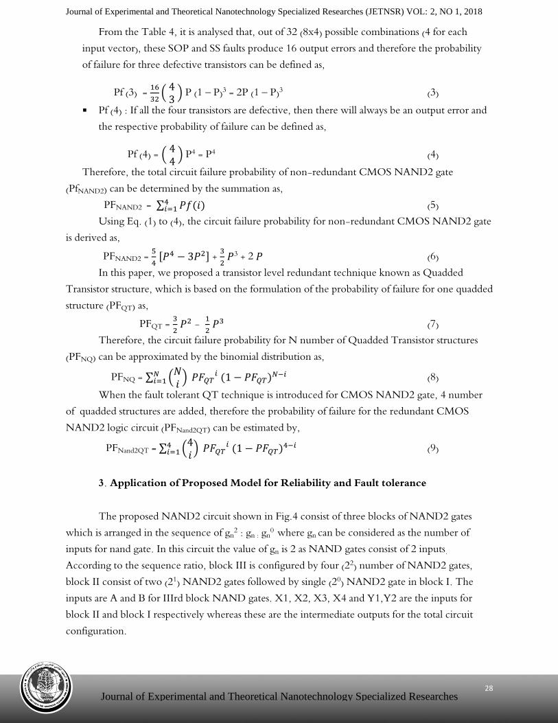
From the Table 4, it is analysed that, out of 32 (8x4) possible combinations (4 for each input vector), these SOP and SS faults produce 16 output errors and therefore the probability of failure for three defective transistors can be defined as,
Pf (3) = 16
32(
43
) P (1 – P)3 = 2P (1 – P)3 (3) Pf (4) : If all the four transistors are defective, then there will always be an output error and
the respective probability of failure can be defined as,
Pf (4) = ( 44
) P4 = P4 (4) Therefore, the total circuit failure probability of non-redundant CMOS NAND2 gate
(PfNAND2) can be determined by the summation as, PFNAND2 = ∑ 𝑃𝑓(𝑖)4
𝑖=1 (5) Using Eq. (1) to (4), the circuit failure probability for non-redundant CMOS NAND2 gate
is derived as, PFNAND2 = 5
4 [𝑃4 − 3𝑃2] + 3
2 𝑃3 + 2 𝑃 (6)
In this paper, we proposed a transistor level redundant technique known as Quadded Transistor structure, which is based on the formulation of the probability of failure for one quadded structure (PFQT) as, PFQT = 3
2 𝑃2 - 1
2 𝑃3 (7)
Therefore, the circuit failure probability for N number of Quadded Transistor structures (PFNQ) can be approximated by the binomial distribution as, PFNQ = ∑ (
𝑁𝑖
) 𝑃𝐹𝑄𝑇𝑖 (1 − 𝑃𝐹𝑄𝑇)𝑁−𝑖𝑁
𝑖=1 (8) When the fault tolerant QT technique is introduced for CMOS NAND2 gate, 4 number
of quadded structures are added, therefore the probability of failure for the redundant CMOS NAND2 logic circuit (PFNand2QT) can be estimated by, PFNand2QT = ∑ (
4𝑖
) 𝑃𝐹𝑄𝑇𝑖 (1 − 𝑃𝐹𝑄𝑇)4−𝑖4
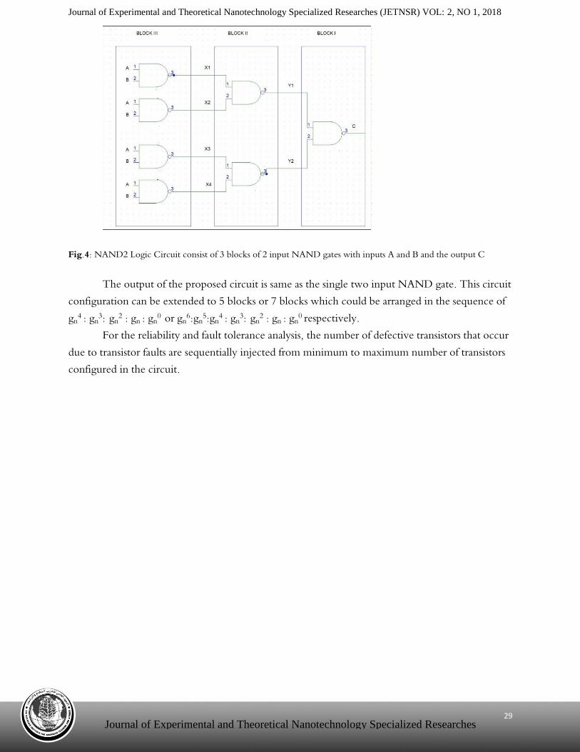
𝑖=1 (9) 3. Application of Proposed Model for Reliability and Fault tolerance The proposed NAND2 circuit shown in Fig.4 consist of three blocks of NAND2 gates
which is arranged in the sequence of gn2 : gn : gn0 where gn can be considered as the number of inputs for nand gate. In this circuit the value of gn is 2 as NAND gates consist of 2 inputs.
According to the sequence ratio, block III is configured by four (22) number of NAND2 gates, block II consist of two (21) NAND2 gates followed by single (20) NAND2 gate in block I. The inputs are A and B for IIIrd block NAND gates. X1, X2, X3, X4 and Y1,Y2 are the inputs for block II and block I respectively whereas these are the intermediate outputs for the total circuit configuration.
Journal of Experimental and Theoretical Nanotechnology Specialized Researches (JETNSR) VOL: 2, NO 1, 2018
01
Journal of Experimental and Theoretical Nanotechnology Specialized Researches
Fig.4: NAND2 Logic Circuit consist of 3 blocks of 2 input NAND gates with inputs A and B and the output C
The output of the proposed circuit is same as the single two input NAND gate. This circuit configuration can be extended to 5 blocks or 7 blocks which could be arranged in the sequence of gn4 : gn3: gn2 : gn : gn0 or gn6:gn5:gn4 : gn3: gn2 : gn : gn0 respectively.
For the reliability and fault tolerance analysis, the number of defective transistors that occur due to transistor faults are sequentially injected from minimum to maximum number of transistors configured in the circuit.
Journal of Experimental and Theoretical Nanotechnology Specialized Researches (JETNSR) VOL: 2, NO 1, 2018
22
Journal of Experimental and Theoretical Nanotechnology Specialized Researches
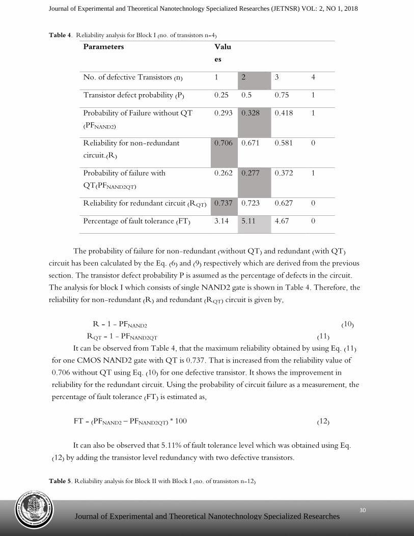
Table 4. Reliability analysis for Block I (no. of transistors n=4)
Parameters Values
No. of defective Transistors (n) 1 2 3 4
Transistor defect probability (P) 0.25 0.5 0.75 1
Probability of Failure without QT (PFNAND2)
0.293 0.328 0.418 1
Reliability for non-redundant circuit.(R)
0.706 0.671 0.581 0
Probability of failure with QT(PFNAND2QT)
0.262 0.277 0.372 1
Reliability for redundant circuit (RQT) 0.737 0.723 0.627 0
Percentage of fault tolerance (FT) 3.14 5.11 4.67 0
The probability of failure for non-redundant (without QT) and redundant (with QT)
circuit has been calculated by the Eq. (6) and (9) respectively which are derived from the previous section. The transistor defect probability P is assumed as the percentage of defects in the circuit. The analysis for block I which consists of single NAND2 gate is shown in Table 4. Therefore, the reliability for non-redundant (R) and redundant (RQT) circuit is given by,
R = 1 - PFNAND2 (10) RQT = 1 - PFNAND2QT (11) It can be observed from Table 4, that the maximum reliability obtained by using Eq. (11)
for one CMOS NAND2 gate with QT is 0.737. That is increased from the reliability value of 0.706 without QT using Eq. (10) for one defective transistor. It shows the improvement in reliability for the redundant circuit. Using the probability of circuit failure as a measurement, the percentage of fault tolerance (FT) is estimated as, FT = (PFNAND2 – PFNAND2QT) * 100 (12)
It can also be observed that 5.11% of fault tolerance level which was obtained using Eq. (12) by adding the transistor level redundancy with two defective transistors.
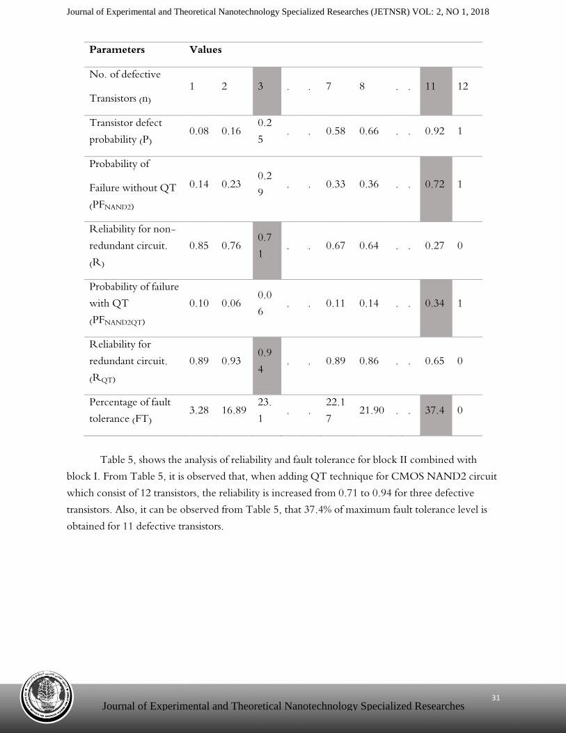
Table 5. Reliability analysis for Block II with Block I (no. of transistors n=12)
Journal of Experimental and Theoretical Nanotechnology Specialized Researches (JETNSR) VOL: 2, NO 1, 2018
26
Journal of Experimental and Theoretical Nanotechnology Specialized Researches
Parameters Values
No. of defective
Transistors (n) 1 2 3 . . 7 8 . . 11 12
Transistor defect probability (P) 0.08 0.16
0.25
. . 0.58 0.66 . . 0.92 1
Probability of
Failure without QT (PFNAND2)
0.14 0.23 0.29
. . 0.33 0.36 . . 0.72 1
Reliability for non-redundant circuit. (R)
0.85 0.76 0.71 . . 0.67 0.64 . . 0.27 0
Probability of failure with QT (PFNAND2QT)
0.10 0.06 0.06 . . 0.11 0.14 . . 0.34 1
Reliability for redundant circuit. (RQT)
0.89 0.93 0.94
. . 0.89 0.86 . . 0.65 0
Percentage of fault tolerance (FT) 3.28 16.89 23.
1 . . 22.1
7 21.90 . . 37.4 0
Table 5, shows the analysis of reliability and fault tolerance for block II combined with
block I. From Table 5, it is observed that, when adding QT technique for CMOS NAND2 circuit which consist of 12 transistors, the reliability is increased from 0.71 to 0.94 for three defective transistors. Also, it can be observed from Table 5, that 37.4% of maximum fault tolerance level is obtained for 11 defective transistors.
Journal of Experimental and Theoretical Nanotechnology Specialized Researches (JETNSR) VOL: 2, NO 1, 2018
20
Journal of Experimental and Theoretical Nanotechnology Specialized Researches
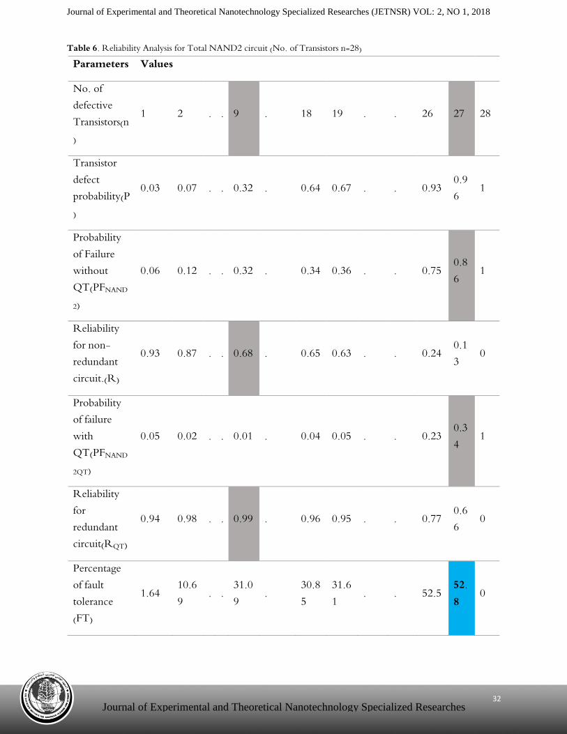
Table 6. Reliability Analysis for Total NAND2 circuit (No. of Transistors n=28)
Parameters Values
No. of defective Transistors(n)
1 2 . . 9 . 18 19 . . 26 27 28
Transistor defect probability(P)
0.03 0.07 . . 0.32 . 0.64 0.67 . . 0.93 0.96 1
Probability of Failure without QT(PFNAND
2)
0.06 0.12 . . 0.32 . 0.34 0.36 . . 0.75 0.86
1
Reliability for non-redundant circuit.(R)
0.93 0.87 . . 0.68 . 0.65 0.63 . . 0.24 0.13
0
Probability of failure with QT(PFNAND
2QT)
0.05 0.02 . . 0.01 . 0.04 0.05 . . 0.23 0.34
1
Reliability for redundant circuit(RQT)
0.94 0.98 . . 0.99 . 0.96 0.95 . . 0.77 0.66
0
Percentage of fault tolerance (FT)
1.64 10.69
. . 31.09
. 30.85
31.61
. . 52.5 52.8
0
Journal of Experimental and Theoretical Nanotechnology Specialized Researches (JETNSR) VOL: 2, NO 1, 2018
22
Journal of Experimental and Theoretical Nanotechnology Specialized Researches
Table 6, shows the analysis of reliability and fault tolerance for the total NAND2 logic circuit. When introducing the QT technique for CMOS NAND2 circuit which consist of 28 transistors, the reliability is increased from 0.68 to 0.99 with nine defective transistors as shown in Table 6. Also, it is observed from Table 6, that the maximum fault tolerance level of 52.8% was achieved for the proposed redundant CMOS NAND2 logic circuit.
4. Simulation and Discussion MATLAB tool is used to simulate the probability of circuit failure with respect to the
transistor defect probability P. The transistor defect probability P is assumed as the percentage of defects that occur in the circuit. So this can be estimated by the number of defective transistors (n) in the CMOS NAND2 logic circuit. Therefore the input parameter for the simulation is the number of defective transistors (n) which is sequentially injected from minimum to maximum value in the CMOS NAND2 logic circuit. And also Eq. (6) and (9) are used for the calculation of probability of failure for non-redundant and redundant CMOS NAND2 logic circuit from the approximation of binomial distribution.
Analysis shows the comparison of circuit failure probability for non-redundant and redundant QT model versus the transistor defect probability P for one, two and three blocks of CMOS NAND2 logic gates which was described in the previous section.
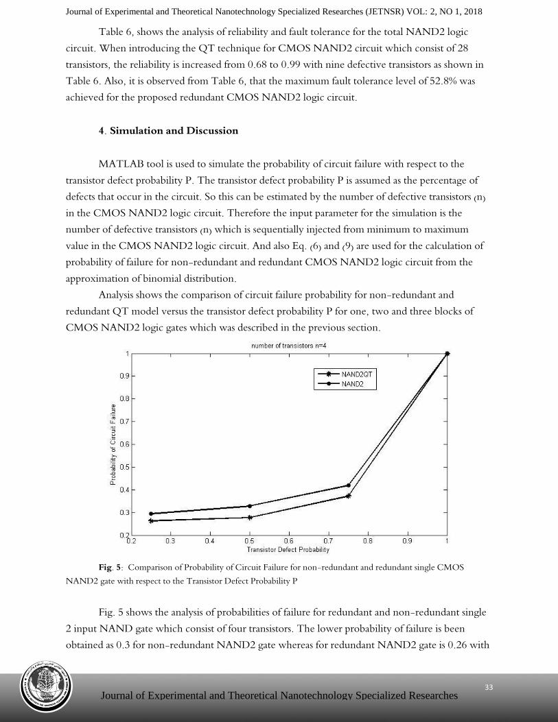
Fig. 5: Comparison of Probability of Circuit Failure for non-redundant and redundant single CMOS
NAND2 gate with respect to the Transistor Defect Probability P Fig. 5 shows the analysis of probabilities of failure for redundant and non-redundant single
2 input NAND gate which consist of four transistors. The lower probability of failure is been obtained as 0.3 for non-redundant NAND2 gate whereas for redundant NAND2 gate is 0.26 with
Journal of Experimental and Theoretical Nanotechnology Specialized Researches (JETNSR) VOL: 2, NO 1, 2018
22
Journal of Experimental and Theoretical Nanotechnology Specialized Researches
one defective transistor. The maximum difference between the probability of failure for redundant and non-redundant NAND2 gate is been obtained as 0.051 with two defective transistors. That results the maximum fault tolerance level as 5.11%.
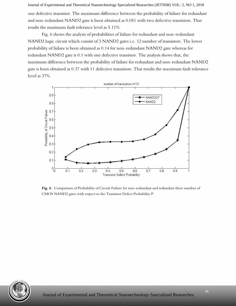
Fig. 6 shows the analysis of probabilities of failure for redundant and non-redundant NAND2 logic circuit which consist of 3 NAND2 gates i.e. 12 number of transistors. The lower probability of failure is been obtained as 0.14 for non-redundant NAND2 gate whereas for redundant NAND2 gate is 0.1 with one defective transistor. The analysis shows that, the maximum difference between the probability of failure for redundant and non-redundant NAND2 gate is been obtained as 0.37 with 11 defective transistors. That results the maximum fault tolerance level as 37%.
Fig. 6: Comparison of Probability of Circuit Failure for non-redundant and redundant three number of CMOS NAND2 gates with respect to the Transistor Defect Probability P
Journal of Experimental and Theoretical Nanotechnology Specialized Researches (JETNSR) VOL: 2, NO 1, 2018
22
Journal of Experimental and Theoretical Nanotechnology Specialized Researches
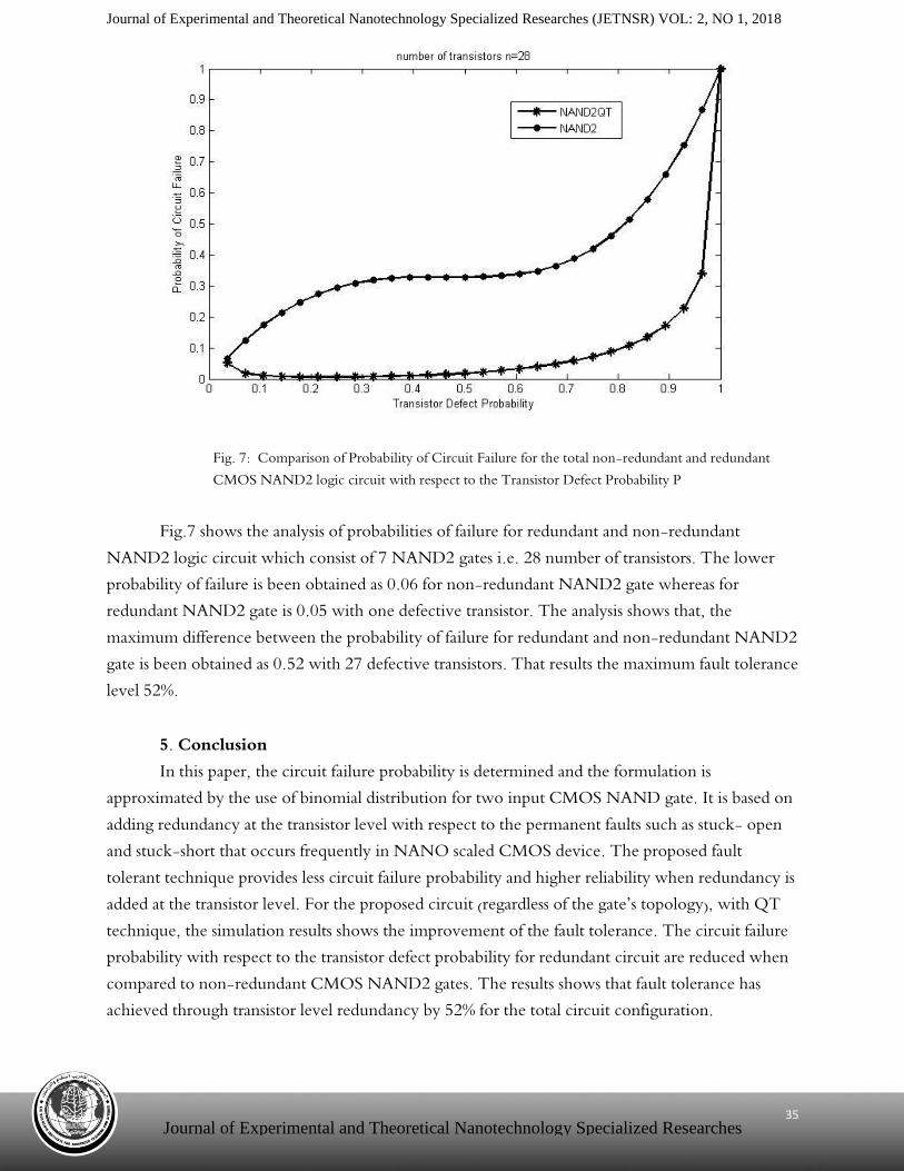
Fig. 7: Comparison of Probability of Circuit Failure for the total non-redundant and redundant CMOS NAND2 logic circuit with respect to the Transistor Defect Probability P
Fig.7 shows the analysis of probabilities of failure for redundant and non-redundant
NAND2 logic circuit which consist of 7 NAND2 gates i.e. 28 number of transistors. The lower probability of failure is been obtained as 0.06 for non-redundant NAND2 gate whereas for redundant NAND2 gate is 0.05 with one defective transistor. The analysis shows that, the maximum difference between the probability of failure for redundant and non-redundant NAND2 gate is been obtained as 0.52 with 27 defective transistors. That results the maximum fault tolerance level 52%.
5. Conclusion
In this paper, the circuit failure probability is determined and the formulation is approximated by the use of binomial distribution for two input CMOS NAND gate. It is based on adding redundancy at the transistor level with respect to the permanent faults such as stuck- open and stuck-short that occurs frequently in NANO scaled CMOS device. The proposed fault tolerant technique provides less circuit failure probability and higher reliability when redundancy is added at the transistor level. For the proposed circuit (regardless of the gate’s topology), with QT technique, the simulation results shows the improvement of the fault tolerance. The circuit failure probability with respect to the transistor defect probability for redundant circuit are reduced when compared to non-redundant CMOS NAND2 gates. The results shows that fault tolerance has achieved through transistor level redundancy by 52% for the total circuit configuration.
Journal of Experimental and Theoretical Nanotechnology Specialized Researches (JETNSR) VOL: 2, NO 1, 2018
21
Journal of Experimental and Theoretical Nanotechnology Specialized Researches
References
[1] A Chaudhry, J N Roy, Gate Oxide Leakage in Poly-depleted Nano-scale MOSFET: A Quantum Mechanical study, Int. J. Nanoelectronics and Materials, 4, 93-100, (2011).
[2] I Saad, M L P Tan, M T Ahmadi, Razali, Ismail, V K Arora, The Dependence of Saturation Velocity on temperature, inversion charge and electric field in a Nanoscale MOSFET, Int. J. Nanoelectronics and Materials, 3, 17-34, (2010).
[3] W Rao, A Orailoglu, R Karri, Fault Tolerant Approaches to Nanoelectronic Programmable Logic Arrays, IEEE Comp Soci, 37th Annual IEEE/IFIP International Conference on Dependable Systems and Networks, 216-224, (2007).
[4] N Miskov-Zivanov and D Marculescu, Circuit Reliability Analysis using Symbolic Techniques, IEEE Trans on Computer Aided Design of Integrated Circuits and Systems, 25, 2638-2649, (2006).
[5] J. Han, J Gao, P Jonker, Y Qi, J A B Fortes, Toward Hardware-Redundant, Fault-Tolerant Logic for Nanoelectronics, IEEE Design & Test of Computers, 22,328-339, (2005).
[6] V Beiu and W Ibrahim, Devices and Input Vectors are Shaping Von Neumann
Multiplexing, IEEE Trans on Nanotechnology, 10, 606-616, (2011).
[7] P Balasubramanian and N E Mastorakis, A Standard Cell Based Voter for use in TMR
Implementation, 5th Euro Conf of Circuits Technology and Devices, 115 – 124, (2014).
[8] T Singh, F Pasaie, R Kumar, Redundancy Based Design and Analysis of ALU Circuit Using CMOS 180nm Process Technology for Fault Tolerant Computing Architectures, Intl J of Computing and Digital Systems, 4, 53 – 62, (2015).
[9] M Stanisavljevic, A Schmid, Y Leblebici, Optimization of nanoelectronic systems reliability under massive defect density using cascaded R-fold modular redundancy, J.Nanotechnology, 19, 465202, (2008).
[10] M Stanisavljevic, A Schmid, Y Leblebici, Optimization of the averaging reliability technique using low redundancy factors for nanoscale technologies, IEEE Trans. On Nanotech., 8, 379–390, (2009).
Journal of Experimental and Theoretical Nanotechnology Specialized Researches (JETNSR) VOL: 2, NO 1, 2018
21
Journal of Experimental and Theoretical Nanotechnology Specialized Researches
[11] M Stanisavljevic, A Schmid, Y Leblebici, “Optimization of Nanoelectronic Systems Reliability Under Massive Defect Density Using Distributed R- fold Modular Redundancy (DRMR), IEEE Comp Soci, 24th IEEE Intl Symp on Defect and Fault Tolerance in VLSI Systems, 340-348, (2009).
[12] W Ibrahim, V Beiu, Using Bayesian Networks to Accurately Calculate the Reliability of Complementary Metal Oxide Semiconductor Gates, IEEE Trans on Reliability, 60, 538-549, (2011).
[13] W Ibrahim, V Beiu, A Bag, Optimum Reliability Sizing for Complementary Metal Oxide Semiconductor Gates, 61, 675-686, (2012).
[14] N Goyal, R Singla, P Goyal, Study and analysis of Universal Gates using Stacking Low Power Technique, Intl J of Computer Science and Information Technologies, 5, 4200-4204, (2014).
[15] J Han, E Leung, L Liu, F Lombardi, A Fault Tolerant Technique using Quadded Logic and Quadded Transistors, IEEE Trans on VLSI Systems, 23, 1562-1566, (2015).
[16] A H El-Maleh, B M Al-Hashimi, A Melouki, F Khan, Defect Tolerant N2 Transistor Structure for Reliable Nanoelectronic Designs”, IET Computers and Digital Techniques, 3, 570-580, (2009).
[17] P Schiefer, R McWilliam, A Purvis, Fault Tolerant Quadded Logic Cell Structure with Built-in Adaptive time Redundancy”, 3rd Intl Conf on Through – Life Engineering Services, 22, 127-131, (2014).
Journal of Experimental and Theoretical Nanotechnology Specialized Researches (JETNSR) VOL: 2, NO 1, 2018
21
Journal of Experimental and Theoretical Nanotechnology Specialized Researches