an arm cortex-m0 for energy harvesting systems: …...an arm cortex-m0 for energy harvesting...
TRANSCRIPT
An ARM Cortex-M0 for Energy Harvesting Systems:
A Novel Application of UPF with Synopsys’ Galaxy Platform
Jatin Mistry James Myers
School of Electronics and Computer Science University of Southampton, UK
www.ecs.soton.ac.uk
and
ARM Ltd Cambridge, UK www.arm.com
ABSTRACT
In energy harvesting systems, energy is effectively infinite but output power is severely limited. In this paper we first present a novel state retention power gating technique, called Sub-Clock Power Gating, which addresses this ultra-low power budget. It works in synergy with voltage and frequency scaling and power gates combinational logic within the clock cycle to reduce ac-tive power. Secondly, we describe how the technique was implemented on an ARM Cortex-M0™ microprocessor for fabrication and discuss our experience of using UPF with Synopsys' Galaxy Platform to achieve the required power gating. Finally, silicon measured results are given.
SNUG 2012 2 ARM Cortex-M0 for Energy Harvesting Systems
Table of Contents 1 Introduction .............................................................................................................................. 3
2 Design Challenge ..................................................................................................................... 4 2.1 SUB-CLOCK POWER GATING TECHNIQUE ........................................................................... 4 2.2 TEST CHIP ........................................................................................................................... 6
3 Design Flow ............................................................................................................................. 8 3.1 INITIAL SYNTHESIS ............................................................................................................. 9 3.2 NETLIST PARSING ............................................................................................................... 9 3.3 SYNTHESIS ........................................................................................................................ 10 3.4 FLOORPLANNING .............................................................................................................. 11 3.5 PLACE AND ROUTE ........................................................................................................... 12 3.6 VERIFICATION .................................................................................................................. 12
4 Results .................................................................................................................................... 14 4.1 SIMULATION ..................................................................................................................... 14 4.2 SILICON ............................................................................................................................ 15
5 Conclusion .............................................................................................................................. 16
6 References .............................................................................................................................. 16 Appendix A – Sub-Clock Cortex-M0 UPF Script ........................................................................ 17
Table of Figures Figure 1 - Idle Time Resulting from Operating at Less than Max. Frequency ............................... 4
Figure 2 - Sub-Clock Power Gating Architecture ........................................................................... 5 Figure 3 - Isolation Control Circuit ................................................................................................ 5
Figure 4 - Sub-Clock Power Gating Timing ................................................................................... 6 Figure 5 - Power Domains within the SCPG Cortex-M0 Macro .................................................... 7
Figure 6 - Design Flow ................................................................................................................... 8 Figure 7 - Information Pulled by the Perl Script from Gate Definitions in the GTECH Netlist .. 10
Figure 8 - Floorplan of Sub-Clock Power Gated Cortex-M0 macro ............................................ 11 Figure 9 - Complete Sub-Clock Cortex-M0 Macro and Full Test Chip Plot ................................ 13
Figure 10 - Activation and Deactivation of Combinational Output Isolation .............................. 14 Figure 11 - Simulated and Measured Power Savings for Different Modes of Operation at Different Frequencies .................................................................................................................... 15 Figure 12 - Oscilloscope Capture of Virtual Rails (VVDD in blue, VVSS in red) in SCPG (left) and SCSTPG (right) ...................................................................................................................... 15
Table of Tables
Table 1 - Power Gating Control Signals of Sub-Clock Cortex-M0 Macro .................................... 7

SNUG 2012 3 ARM Cortex-M0 for Energy Harvesting Systems
1 Introduction Mobile devices are typically powered by one of two methods: there are those that rely on stored energy, such as batteries, and those that are powered by energy harvesters. Devices powered by batteries are constrained to the finite energy that can be kept in the energy storage element. Once the battery is depleted, it is necessary to then replace or recharge the energy stored such that the device can continue to be used. On the other hand, energy harvesting continuously scavenges energy from the environment and for that reason provides an infinite trickle of energy to the sys-tem eliminating the need to service batteries [1]. This advantage of energy harvesting over bat-teries makes it particularly useful for applications such as Wireless Sensor Networks where small devices can be expected to operate, without maintenance, for months or even years [1]. However, although the supply of energy is infinite from an energy harvester, its power output is limited by how much energy it can scavenge. For this reason, to maintain throughput of the processing sys-tem, the power draw should be equal to or less than the power output of the harvester, requiring ultra-low active power. Dynamic power can be successfully reduced with the application of voltage and frequency scal-ing [2] but leakage power is a growing concern in nanometre technologies. It has been shown that at sub-65nm technologies, leakage can be as high as dynamic power and therefore presents a major challenge in mobile devices [3]. A number of solutions have been proposed to reduce leakage power dissipation but power gating is amongst the most practical [2]. Power gating pro-vides a solution to minimising leakage currents during extended periods of idle time by discon-necting the supply to subsections of a system by means of a header or footer power gating tran-sistor. Leakage, however, can be a significant drain of power during active mode. In this paper we describe a technique of power gating, called Sub-Clock Power Gating [4], that can be used concurrently with voltage and frequency scaling to simultaneously reduce active mode dynamic and leakage power. The technique described, aggressively scales the clock frequency of the sys-tem and uses power gating to shut down combinational logic within the clock cycle resulting in a lower average power capable of matching the output power of an energy harvester. The Sub-Clock Power Gating technique has been validated through implementation on an ARM Cortex-M0™ microprocessor, fabricated using a 65nm process. The application of power gating within a digital circuit is now well supported in the Synopsys Galaxy design flow with the addi-tion of the Unified Power Format (UPF), a leading power design intent standard [5][6]. Howev-er, the Sub-Clock Power Gating technique is unlike traditional power gating and presented a number of design challenges during implementation. This paper describes how the versatility of UPF was exploited to achieve the power gating required. The paper is a result of collaborative work between The University of Southampton and ARM Ltd, who kindly granted access to the Cortex-M0 processor used. The use of Synopsys tools was only possible with the award of the Charles Babbage Grant from Synopsys Inc to The University of Southampton in 2009. The fab-rication of the test chip was achieved through the Europractice Mini@sic Multi-Project Wafer (MPW) scheme [7] with support from the EPSRC-UK Holistic Energy Harvesting project, grant number EP/G067740/1 [8].
SNUG 2012 4 ARM Cortex-M0 for Energy Harvesting Systems
2 Design Challenge
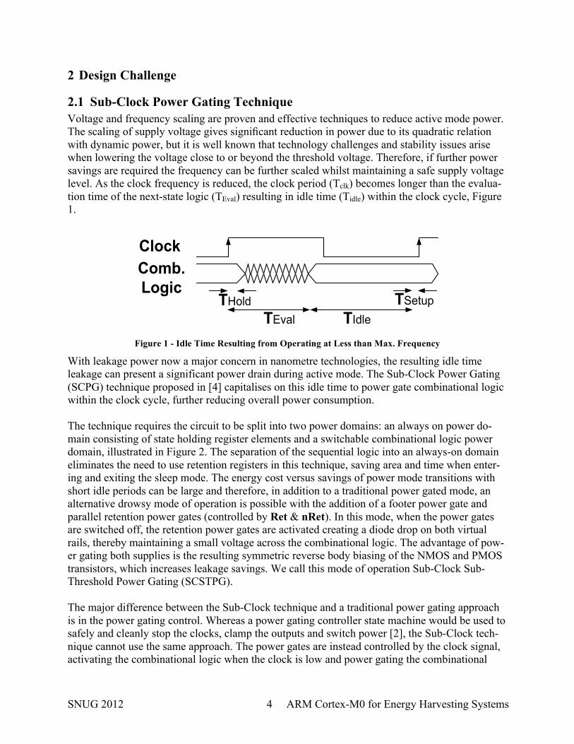
2.1 Sub-Clock Power Gating Technique Voltage and frequency scaling are proven and effective techniques to reduce active mode power. The scaling of supply voltage gives significant reduction in power due to its quadratic relation with dynamic power, but it is well known that technology challenges and stability issues arise when lowering the voltage close to or beyond the threshold voltage. Therefore, if further power savings are required the frequency can be further scaled whilst maintaining a safe supply voltage level. As the clock frequency is reduced, the clock period (Tclk) becomes longer than the evalua-tion time of the next-state logic (TEval) resulting in idle time (Tidle) within the clock cycle, Figure 1.
Figure 1 - Idle Time Resulting from Operating at Less than Max. Frequency
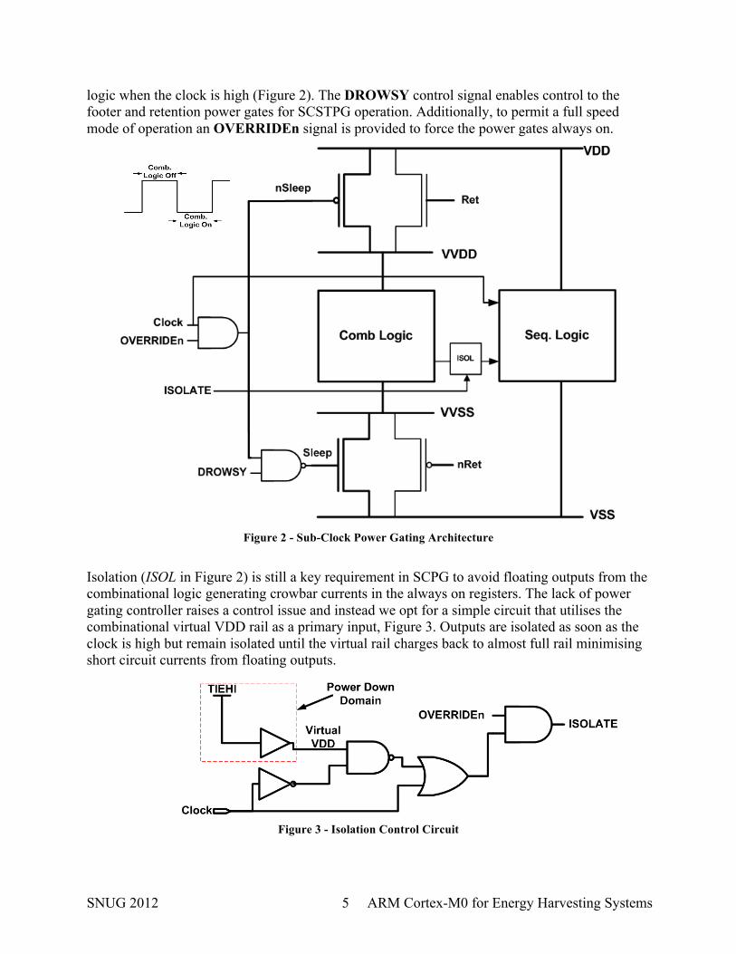
With leakage power now a major concern in nanometre technologies, the resulting idle time leakage can present a significant power drain during active mode. The Sub-Clock Power Gating (SCPG) technique proposed in [4] capitalises on this idle time to power gate combinational logic within the clock cycle, further reducing overall power consumption. The technique requires the circuit to be split into two power domains: an always on power do-main consisting of state holding register elements and a switchable combinational logic power domain, illustrated in Figure 2. The separation of the sequential logic into an always-on domain eliminates the need to use retention registers in this technique, saving area and time when enter-ing and exiting the sleep mode. The energy cost versus savings of power mode transitions with short idle periods can be large and therefore, in addition to a traditional power gated mode, an alternative drowsy mode of operation is possible with the addition of a footer power gate and parallel retention power gates (controlled by Ret & nRet). In this mode, when the power gates are switched off, the retention power gates are activated creating a diode drop on both virtual rails, thereby maintaining a small voltage across the combinational logic. The advantage of pow-er gating both supplies is the resulting symmetric reverse body biasing of the NMOS and PMOS transistors, which increases leakage savings. We call this mode of operation Sub-Clock Sub-Threshold Power Gating (SCSTPG). The major difference between the Sub-Clock technique and a traditional power gating approach is in the power gating control. Whereas a power gating controller state machine would be used to safely and cleanly stop the clocks, clamp the outputs and switch power [2], the Sub-Clock tech-nique cannot use the same approach. The power gates are instead controlled by the clock signal, activating the combinational logic when the clock is low and power gating the combinational
THoldTEval
TSetupTIdle
ClockComb. Logic
SNUG 2012 5 ARM Cortex-M0 for Energy Harvesting Systems
logic when the clock is high (Figure 2). The DROWSY control signal enables control to the footer and retention power gates for SCSTPG operation. Additionally, to permit a full speed mode of operation an OVERRIDEn signal is provided to force the power gates always on.
Figure 2 - Sub-Clock Power Gating Architecture
Isolation (ISOL in Figure 2) is still a key requirement in SCPG to avoid floating outputs from the combinational logic generating crowbar currents in the always on registers. The lack of power gating controller raises a control issue and instead we opt for a simple circuit that utilises the combinational virtual VDD rail as a primary input, Figure 3. Outputs are isolated as soon as the clock is high but remain isolated until the virtual rail charges back to almost full rail minimising short circuit currents from floating outputs.
Figure 3 - Isolation Control Circuit
SNUG 2012 6 ARM Cortex-M0 for Energy Harvesting Systems
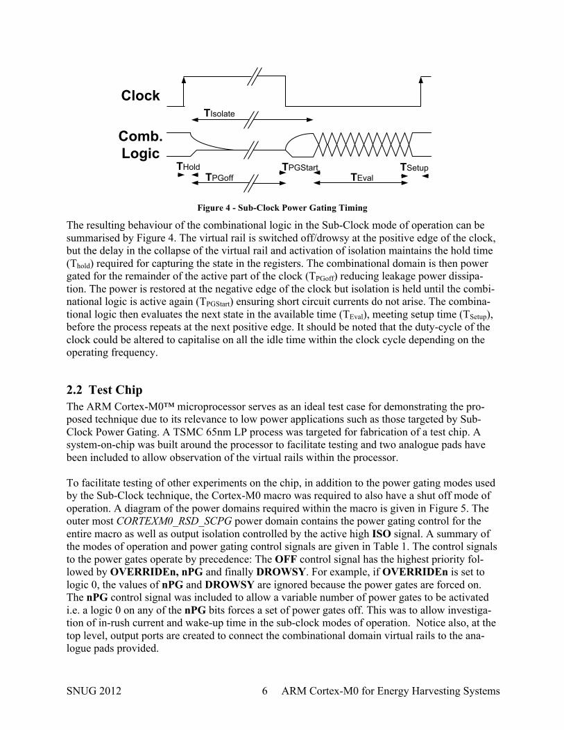
Figure 4 - Sub-Clock Power Gating Timing
The resulting behaviour of the combinational logic in the Sub-Clock mode of operation can be summarised by Figure 4. The virtual rail is switched off/drowsy at the positive edge of the clock, but the delay in the collapse of the virtual rail and activation of isolation maintains the hold time (Thold) required for capturing the state in the registers. The combinational domain is then power gated for the remainder of the active part of the clock (TPGoff) reducing leakage power dissipa-tion. The power is restored at the negative edge of the clock but isolation is held until the combi-national logic is active again (TPGStart) ensuring short circuit currents do not arise. The combina-tional logic then evaluates the next state in the available time (TEval), meeting setup time (TSetup), before the process repeats at the next positive edge. It should be noted that the duty-cycle of the clock could be altered to capitalise on all the idle time within the clock cycle depending on the operating frequency.
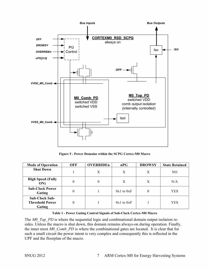
2.2 Test Chip The ARM Cortex-M0™ microprocessor serves as an ideal test case for demonstrating the pro-posed technique due to its relevance to low power applications such as those targeted by Sub-Clock Power Gating. A TSMC 65nm LP process was targeted for fabrication of a test chip. A system-on-chip was built around the processor to facilitate testing and two analogue pads have been included to allow observation of the virtual rails within the processor. To facilitate testing of other experiments on the chip, in addition to the power gating modes used by the Sub-Clock technique, the Cortex-M0 macro was required to also have a shut off mode of operation. A diagram of the power domains required within the macro is given in Figure 5. The outer most CORTEXM0_RSD_SCPG power domain contains the power gating control for the entire macro as well as output isolation controlled by the active high ISO signal. A summary of the modes of operation and power gating control signals are given in Table 1. The control signals to the power gates operate by precedence: The OFF control signal has the highest priority fol-lowed by OVERRIDEn, nPG and finally DROWSY. For example, if OVERRIDEn is set to logic 0, the values of nPG and DROWSY are ignored because the power gates are forced on. The nPG control signal was included to allow a variable number of power gates to be activated i.e. a logic 0 on any of the nPG bits forces a set of power gates off. This was to allow investiga-tion of in-rush current and wake-up time in the sub-clock modes of operation. Notice also, at the top level, output ports are created to connect the combinational domain virtual rails to the ana-logue pads provided.
TIsolate
TPGoff TEvalTHold TSetupTPGStart
Clock
Comb. Logic
SNUG 2012 7 ARM Cortex-M0 for Energy Harvesting Systems
Figure 5 - Power Domains within the SCPG Cortex-M0 Macro
Mode of Operation OFF OVERRIDEn nPG DROWSY State Retained
Shut Down 1 X X X NO
High Speed (Fully ON) 0 0 X X N/A
Sub-Clock Power Gating 0 1 0x1 to 0xF 0 YES
Sub-Clock Sub-Threshold Power
Gating 0 1 0x1 to 0xF 1 YES
Table 1 - Power Gating Control Signals of Sub-Clock Cortex-M0 Macro
The M0_Top_PD is where the sequential logic and combinational domain output isolation re-sides. Unless the macro is shut down, this domain remains always-on during operation. Finally, the inner most M0_Comb_PD is where the combinational gates are located. It is clear that for such a small circuit the power intent is very complex and consequently this is reflected in the UPF and the floorplan of the macro.
SNUG 2012 8 ARM Cortex-M0 for Energy Harvesting Systems
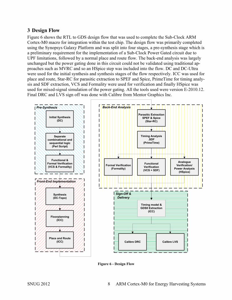
3 Design Flow Figure 6 shows the RTL to GDS design flow that was used to complete the Sub-Clock ARM Cortex-M0 macro for integration within the test chip. The design flow was primarily completed using the Synopsys Galaxy Platform and was split into four stages, a pre-synthesis stage which is a preliminary requirement for the implementation of a Sub-Clock Power Gated circuit due to UPF limitations, followed by a normal place and route flow. The back-end analysis was largely unchanged but the power gating done in this circuit could not be validated using traditional ap-proaches such as MVRC and so an HSpice step was included into the flow. DC and DC-Ultra were used for the initial synthesis and synthesis stages of the flow respectively. ICC was used for place and route, Star-RC for parasitic extraction to SPEF and Spice, PrimeTime for timing analy-sis and SDF extraction, VCS and Formality were used for verification and finally HSpice was used for mixed-signal simulation of the power gating. All the tools used were version E-2010.12. Final DRC and LVS sign off was done with Calibre from Mentor Graphics Inc.
Initial Synthesis(DC)
Separate combinational and
sequential logic(Perl Script)
Synthesis(DC-Topo)
Floorplanning(ICC)
Parasitic ExtractionSPEF & Spice
(Star-RC)
Functional Verification(VCS + SDF)
Formal Verification(Formality)
Analogue Verification/
Power Analysis(HSpice)
Timing Analysis.SDF
(PrimeTime)
Timing model & GDSII Extraction
(ICC)
Calibre LVSCalibre DRCPlace and Route
(ICC)
Pre-Synthesis
Front-End Implementation
Back-End Analysis
Sign-Off &Delivery
Functional & Formal Verification(VCS & Formality)
Figure 6 - Design Flow
SNUG 2012 9 ARM Cortex-M0 for Energy Harvesting Systems
3.1 Initial Synthesis To implement power gating on a design, logic is grouped in RTL into hierarchical modules such that the power domains can be defined with the UPF command:
create_power_domain “Name” –elements {“hierarchical modules”}
Typically the Verilog would be written with the power intent in mind meaning the above com-mand presents a trivial method to create the power domains. However, when using Sub-Clock Power Gating, the two main power domains consist of the sequential state holding elements, and the combinational logic (Figure 2). Conventionally both sequential and combinational logic re-side in the same modules, which makes the use of the above command difficult for creating the required power domains. A method to assign the combinational and sequential logic to separate power domains was therefore required. The solution to this problem was to reassign the logic to new Verilog modules and the initial synthesis operation shown in Figure 6 was the first of two stages needed to do that. In this operation the RTL design was mapped to the Synopsys GTECH library to simplify identification and assignment of combinational and sequential logic into dif-ferent Verilog modules. This was preferred over mapping the design directly to the target library as a GTECH description of the circuit can be later mapped to different target technologies in-creasing the portability of the flow whilst simultaneously reducing turnaround time. The target library was set to the internal GTECH library, a standard compile was run and a flat gate level Verilog netlist was written out using simple names. The simple names output was an important requirement as it facilitated the use of a Perl script in the second stage to separate the sequential and combinational logic. It was found that synthesising to GTECH and later mapping this netlist to the target library re-sulted in timing closure problems. The root of the problem was traced to the optimisation of arithmetic terms such as multiplication. The limited functionality of gates in the GTECH library resulted in a poor optimization of such terms, which, coupled with synthesis to the target library, resulted in poor timing. Since arithmetic terms are purely combinational, this problem was over-come by capitalising on the modularity of the Cortex-M0 RTL. The modules containing the arithmetic hardware description were set to dont_touch during the initial compile, maintain-ing the hierarchy of these modules within the flat output netlist. This allowed the synthesised versions of these modules to be swapped with the original RTL modules producing better opti-misation in the final synthesis stage.
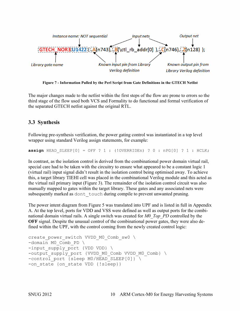
3.2 Netlist Parsing To establish the sequential and combinational modules required by UPF for power domain defi-nition, the netlist from the initial synthesis was parsed using a Perl script. The Perl script reads the netlist line by line and uses the _reg suffix appended by Design Compiler to identify sequen-tial elements. The input and output ports of each gate are learnt from the Verilog definitions in the gtech_lib.v file and the connections to and from each gate are recorded into a tree structure. This allows the netlist to be traversed and connections between the two modules to be main-tained when separating gates into their two different modules. An example of the information captured and used by the Perl script is shown in Figure 7.
SNUG 2012 10 ARM Cortex-M0 for Energy Harvesting Systems
Figure 7 - Information Pulled by the Perl Script from Gate Definitions in the GTECH Netlist
The major changes made to the netlist within the first steps of the flow are prone to errors so the third stage of the flow used both VCS and Formality to do functional and formal verification of the separated GTECH netlist against the original RTL.
3.3 Synthesis Following pre-synthesis verification, the power gating control was instantiated in a top level wrapper using standard Verilog assign statements, for example: assign HEAD_SLEEP[0] = OFF ? 1 : (!OVERRIDEn) ? 0 : nPG[0] ? 1 : HCLK; In contrast, as the isolation control is derived from the combinational power domain virtual rail, special care had to be taken with the circuitry to ensure what appeared to be a constant logic 1 (virtual rail) input signal didn’t result in the isolation control being optimised away. To achieve this, a target library TIEHI cell was placed in the combinational Verilog module and this acted as the virtual rail primary input (Figure 3). The remainder of the isolation control circuit was also manually mapped to gates within the target library. These gates and any associated nets were subsequently marked as dont_touch during compile to prevent unwanted pruning. The power intent diagram from Figure 5 was translated into UPF and is listed in full in Appendix A. At the top level, ports for VDD and VSS were defined as well as output ports for the combi-national domain virtual rails. A single switch was created for M0_Top_PD controlled by the OFF signal. Despite the unusual control of the combinational power gates, they were also de-fined within the UPF, with the control coming from the newly created control logic: create_power_switch VVDD_M0_Comb_sw0 \ -domain M0_Comb_PD \ -input_supply_port {VDD VDD} \ -output_supply_port {VVDD_M0_Comb VVDD_M0_Comb} \ -control_port {sleep M0/HEAD_SLEEP[0]} \ -on_state {on_state VDD {!sleep}}
SNUG 2012 11 ARM Cortex-M0 for Energy Harvesting Systems
Isolation between the power domains was also defined conventionally, but the virtual rail signal from the combinational domain had to be set to no isolation so that it could be propagated from the combinational power domain to the isolation control circuit in the always on power domain. set_isolation M0_Comb_noIso \ -domain M0_Comb_PD \ -elements M0/combinational/VIRTUALRAIL \ -no_isolation
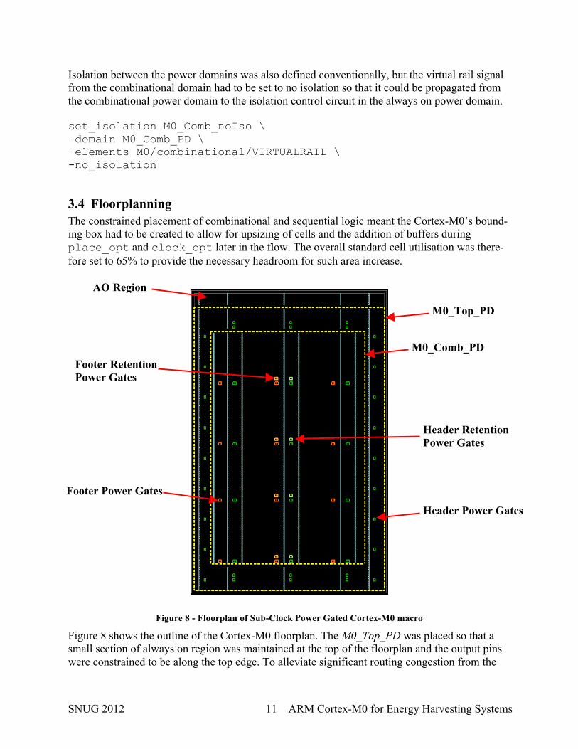
3.4 Floorplanning The constrained placement of combinational and sequential logic meant the Cortex-M0’s bound-ing box had to be created to allow for upsizing of cells and the addition of buffers during place_opt and clock_opt later in the flow. The overall standard cell utilisation was there-fore set to 65% to provide the necessary headroom for such area increase.
Figure 8 - Floorplan of Sub-Clock Power Gated Cortex-M0 macro
Figure 8 shows the outline of the Cortex-M0 floorplan. The M0_Top_PD was placed so that a small section of always on region was maintained at the top of the floorplan and the output pins were constrained to be along the top edge. To alleviate significant routing congestion from the
M0_Top_PD
M0_Comb_PD
AO Region
Header Power Gates
Footer Power Gates
Header Retention Power Gates
Footer Retention Power Gates
SNUG 2012 12 ARM Cortex-M0 for Energy Harvesting Systems
large number of nets connecting between the combinational and sequential logic, the combina-tional logic power domain was placed in the centre of the macro thereby offering the maximum number of routing tracks between the domains. To ensure correct biasing of the wells, N-Well bias cells were used in the M0_Top_PD whereas N-Well and P-Well bias cells were required in the combinational power domain as both supply rails are switched. Power gates were inserted using create_power_switch_array in both the combinational and sequential domains. In the combinational domain 6 header and 6 footer power gates were distributed for each nPG control signal, whereas 2 header retention and 2 footer retention power gates were placed per control signal. Fewer retention switches were needed than power gates as they do not need to supply current for dynamic switching during active operation. The complex power scheme in the macro, consisting of 5 supply nets, was created explicitly with create_power_straps rather than using PNS. This ensured correct always on supply hook-up to the power gates as well as adequate coverage on metal layers.
3.5 Place and Route The place_opt, clock_opt and route_opt stages in the design flow followed a conven-tional implementation flow. Placement was done using place_opt -effort high to min-imise displacement between logically neighbouring gates and improve potential routing conges-tion. Even so, a high number of shorted nets and DRC violations arose during route_opt which were fixed with iterations of the command: route_zrt_detail –incremental true –initial_drc_from_input true
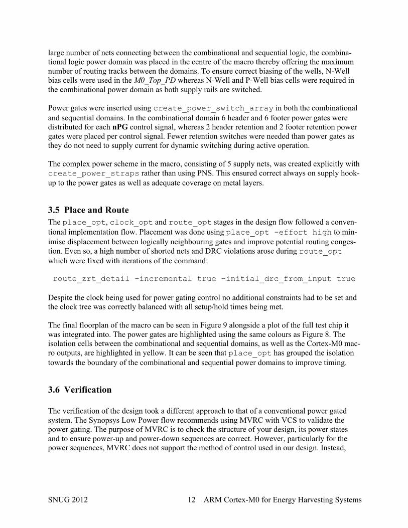
Despite the clock being used for power gating control no additional constraints had to be set and the clock tree was correctly balanced with all setup/hold times being met. The final floorplan of the macro can be seen in Figure 9 alongside a plot of the full test chip it was integrated into. The power gates are highlighted using the same colours as Figure 8. The isolation cells between the combinational and sequential domains, as well as the Cortex-M0 mac-ro outputs, are highlighted in yellow. It can be seen that place_opt has grouped the isolation towards the boundary of the combinational and sequential power domains to improve timing.
3.6 Verification The verification of the design took a different approach to that of a conventional power gated system. The Synopsys Low Power flow recommends using MVRC with VCS to validate the power gating. The purpose of MVRC is to check the structure of your design, its power states and to ensure power-up and power-down sequences are correct. However, particularly for the power sequences, MVRC does not support the method of control used in our design. Instead,
SNUG 2012 13 ARM Cortex-M0 for Energy Harvesting Systems
Figure 9 - Complete Sub-Clock Cortex-M0 Macro and Full Test Chip Plot
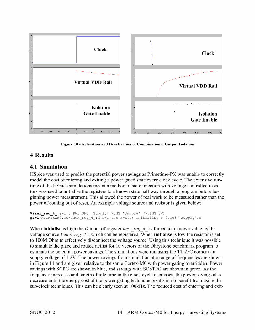
VCS with .SDF was used for purely functional checking of the netlist and Formality was used with the UPF to perform the static checks on the design. The Power State Table (PST) created in the UPF defines the valid power states and can therefore be used by Formality to ensure the power gates and isolation are driven properly in each power state – very similar to what MVRC can achieve. In the case of the power-up and power-down sequences, the only way to check the control to the power gates and isolation was correctly issued was to perform an analogue simulation on the design using HSpice. Most importantly, this simulation checked the isolation was activated and deactivated as expected. The simulation results are shown in Figure 10. The graphs on the left show the activation of the isolation, de-asserting the enable signal as soon as the clock goes high (power off). The graphs on the right show the deactivation of isolation. Notice that the isolation enable signal is not asserted until the virtual rail has charged to two thirds full rail, which is the desired behaviour of using the virtual rail as an input to the isolation control.
SNUG 2012 14 ARM Cortex-M0 for Energy Harvesting Systems
Figure 10 - Activation and Deactivation of Combinational Output Isolation
4 Results
4.1 Simulation HSpice was used to predict the potential power savings as Primetime-PX was unable to correctly model the cost of entering and exiting a power gated state every clock cycle. The extensive run-time of the HSpice simulations meant a method of state injection with voltage controlled resis-tors was used to initialise the registers to a known state half way through a program before be-ginning power measurement. This allowed the power of real work to be measured rather than the power of coming out of reset. An example voltage source and resistor is given below: Viaex_reg_4_ sw1 0 PWL(0NS 'Supply' 75NS 'Supply' 75.1NS 0V) gsw1 xCORTEXM0.M0/iaex_reg_4_:d sw1 VCR PWL(1) initialise 0 0,1e8 'Supply',0
When initialise is high the D input of register iaex_reg_4_ is forced to a known value by the voltage source Viaex_reg_4_, which can be registered. When initialise is low the resistor is set to 100M Ohm to effectively disconnect the voltage source. Using this technique it was possible to simulate the place and routed netlist for 10 vectors of the Dhrystone benchmark program to estimate the potential power savings. The simulations were run using the TT 25C corner at a supply voltage of 1.2V. The power savings from simulation at a range of frequencies are shown in Figure 11 and are given relative to the same Cortex-M0 with power gating overridden. Power savings with SCPG are shown in blue, and savings with SCSTPG are shown in green. As the frequency increases and length of idle time in the clock cycle decreases, the power savings also decrease until the energy cost of the power gating technique results in no benefit from using the sub-clock techniques. This can be clearly seen at 100kHz. The reduced cost of entering and exit-
Clock
Virtual VDD Rail
Isolation Gate Enable
Clock
Virtual VDD Rail
Isolation Gate Enable
SNUG 2012 15 ARM Cortex-M0 for Energy Harvesting Systems
ing the power gated mode in SCSTPG results in higher savings than SCPG across all frequen-cies.
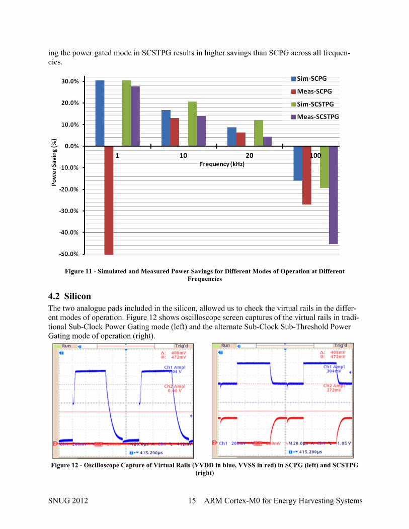
Figure 11 - Simulated and Measured Power Savings for Different Modes of Operation at Different
Frequencies
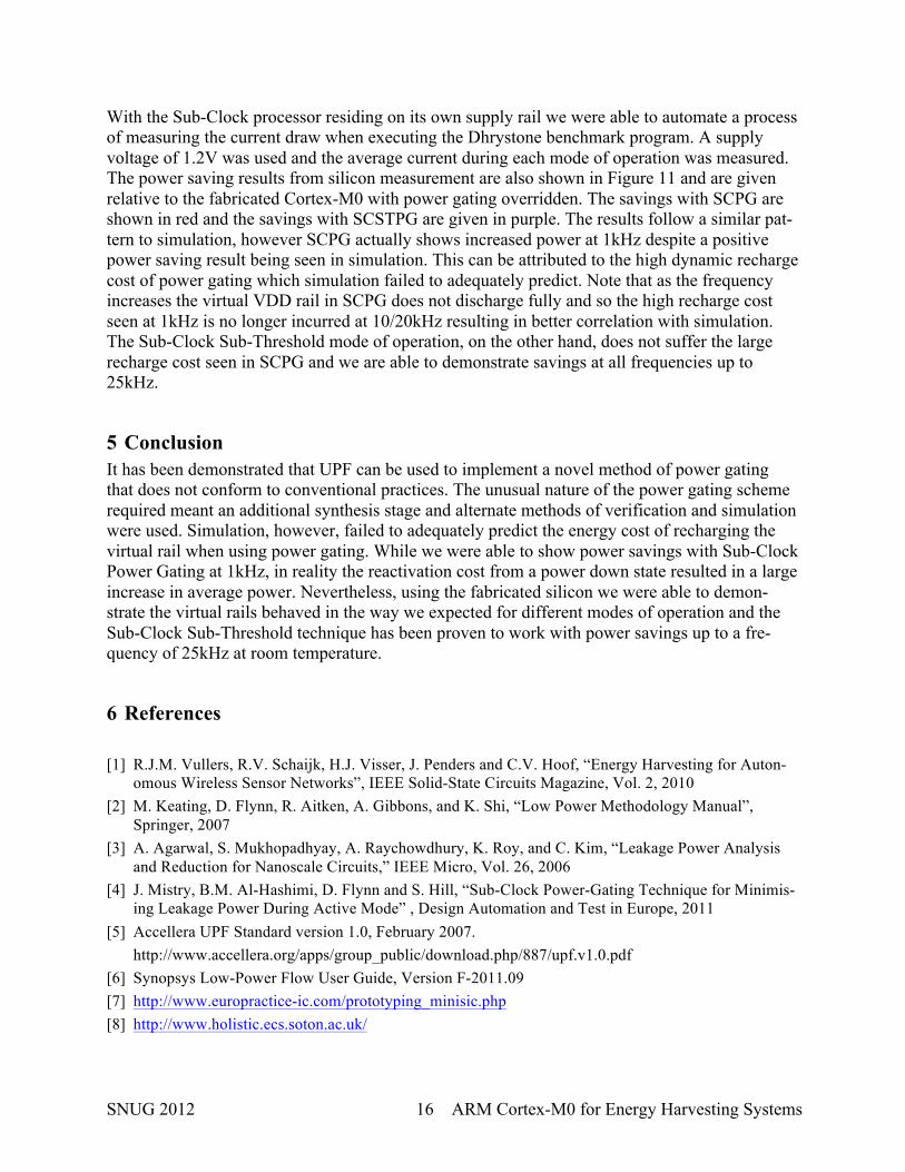
4.2 Silicon The two analogue pads included in the silicon, allowed us to check the virtual rails in the differ-ent modes of operation. Figure 12 shows oscilloscope screen captures of the virtual rails in tradi-tional Sub-Clock Power Gating mode (left) and the alternate Sub-Clock Sub-Threshold Power Gating mode of operation (right).
Figure 12 - Oscilloscope Capture of Virtual Rails (VVDD in blue, VVSS in red) in SCPG (left) and SCSTPG (right)
SNUG 2012 16 ARM Cortex-M0 for Energy Harvesting Systems
With the Sub-Clock processor residing on its own supply rail we were able to automate a process of measuring the current draw when executing the Dhrystone benchmark program. A supply voltage of 1.2V was used and the average current during each mode of operation was measured. The power saving results from silicon measurement are also shown in Figure 11 and are given relative to the fabricated Cortex-M0 with power gating overridden. The savings with SCPG are shown in red and the savings with SCSTPG are given in purple. The results follow a similar pat-tern to simulation, however SCPG actually shows increased power at 1kHz despite a positive power saving result being seen in simulation. This can be attributed to the high dynamic recharge cost of power gating which simulation failed to adequately predict. Note that as the frequency increases the virtual VDD rail in SCPG does not discharge fully and so the high recharge cost seen at 1kHz is no longer incurred at 10/20kHz resulting in better correlation with simulation. The Sub-Clock Sub-Threshold mode of operation, on the other hand, does not suffer the large recharge cost seen in SCPG and we are able to demonstrate savings at all frequencies up to 25kHz.
5 Conclusion It has been demonstrated that UPF can be used to implement a novel method of power gating that does not conform to conventional practices. The unusual nature of the power gating scheme required meant an additional synthesis stage and alternate methods of verification and simulation were used. Simulation, however, failed to adequately predict the energy cost of recharging the virtual rail when using power gating. While we were able to show power savings with Sub-Clock Power Gating at 1kHz, in reality the reactivation cost from a power down state resulted in a large increase in average power. Nevertheless, using the fabricated silicon we were able to demon-strate the virtual rails behaved in the way we expected for different modes of operation and the Sub-Clock Sub-Threshold technique has been proven to work with power savings up to a fre-quency of 25kHz at room temperature.
6 References [1] R.J.M. Vullers, R.V. Schaijk, H.J. Visser, J. Penders and C.V. Hoof, “Energy Harvesting for Auton-
omous Wireless Sensor Networks”, IEEE Solid-State Circuits Magazine, Vol. 2, 2010 [2] M. Keating, D. Flynn, R. Aitken, A. Gibbons, and K. Shi, “Low Power Methodology Manual”,
Springer, 2007 [3] A. Agarwal, S. Mukhopadhyay, A. Raychowdhury, K. Roy, and C. Kim, “Leakage Power Analysis
and Reduction for Nanoscale Circuits,” IEEE Micro, Vol. 26, 2006 [4] J. Mistry, B.M. Al-Hashimi, D. Flynn and S. Hill, “Sub-Clock Power-Gating Technique for Minimis-
ing Leakage Power During Active Mode” , Design Automation and Test in Europe, 2011 [5] Accellera UPF Standard version 1.0, February 2007.
http://www.accellera.org/apps/group_public/download.php/887/upf.v1.0.pdf [6] Synopsys Low-Power Flow User Guide, Version F-2011.09 [7] http://www.europractice-ic.com/prototyping_minisic.php [8] http://www.holistic.ecs.soton.ac.uk/
SNUG 2012 17 ARM Cortex-M0 for Energy Harvesting Systems
Appendix A – Sub-Clock Cortex-M0 UPF Script #----------------------------------------- #Top Power Domain #----------------------------------------- create_power_domain Top_PD -include_scope create_supply_port VDD create_supply_net VDD -domain Top_PD connect_supply_net VDD -ports VDD create_supply_port VSS create_supply_net VSS -domain Top_PD connect_supply_net VSS -ports VSS create_supply_port VVSS_M0_Comb -direction out create_supply_net VVSS_M0_Comb -domain Top_PD -resolve parallel connect_supply_net VVSS_M0_Comb -ports VVSS_M0_Comb create_supply_port VVDD_M0_Comb -direction out create_supply_net VVDD_M0_Comb -domain Top_PD -resolve parallel connect_supply_net VVDD_M0_Comb -ports VVDD_M0_Comb set_domain_supply_net Top_PD \ -primary_power_net VDD \ -primary_ground_net VSS #----------------------------------------- #M0 Top Power Domain #----------------------------------------- create_power_domain M0_Top_PD -elements {M0} create_supply_net VDD -domain M0_Top_PD -reuse create_supply_net VSS -domain M0_Top_PD -reuse create_supply_net VVDD_M0_Top -domain M0_Top_PD -resolve parallel set_domain_supply_net M0_Top_PD \ -primary_power_net VVDD_M0_Top \ -primary_ground_net VSS #----------------------------------------- #M0 Top VVDD Power Switch #----------------------------------------- create_power_switch VVDD_M0_Top_sw \ -domain M0_Top_PD \ -input_supply_port {VDD VDD} \ -output_supply_port {VVDD_M0_Top VVDD_M0_Top} \ -control_port {sleep OFF} \ -on_state {on_state VDD {!sleep}} #----------------------------------------- #M0 Top Outputs Isolation Stategy #----------------------------------------- set_isolation M0_Top_isol \ -domain M0_Top_PD \ -isolation_power_net VDD \
SNUG 2012 18 ARM Cortex-M0 for Energy Harvesting Systems
-isolation_ground_net VSS \ -clamp_value 0 set_isolation_control M0_Top_isol \ -domain M0_Top_PD \ -isolation_signal ISO \ -isolation_sense high \ -location parent set_isolation M0_Top_noIso \ -domain M0_Top_PD \ -elements M0/VIRTUALRAIL \ -no_isolation #----------------------------------------- #M0 Combinational Logic Power Domain #----------------------------------------- create_power_domain M0_Comb_PD -elements {M0/combinational} create_supply_net VDD -domain M0_Comb_PD -reuse create_supply_net VSS -domain M0_Comb_PD -reuse create_supply_net VVSS_M0_Comb -domain M0_Comb_PD -resolve parallel -reuse #Combinational logic drowsy power rail create_supply_net VVDD_M0_Comb -domain M0_Comb_PD -resolve parallel -reuse set_domain_supply_net M0_Comb_PD \ -primary_power_net VVDD_M0_Comb \ -primary_ground_net VVSS_M0_Comb #----------------------------------------- #M0 Combinational Logic VVDD Power Switch & Retention switch #----------------------------------------- create_power_switch VVDD_M0_Comb_sw0 -domain M0_Comb_PD -input_supply_port {VDD VDD} -output_supply_port {VVDD_M0_Comb VVDD_M0_Comb} \ -control_port {sleep M0/HEAD_SLEEP[0]} -on_state {on_state VDD {!sleep}} create_power_switch VVDD_M0_Comb_sw1 -domain M0_Comb_PD -input_supply_port {VDD VDD} -output_supply_port {VVDD_M0_Comb VVDD_M0_Comb} \ -control_port {sleep M0/HEAD_SLEEP[1]} -on_state {on_state VDD {!sleep}} create_power_switch VVDD_M0_Comb_sw2 -domain M0_Comb_PD -input_supply_port {VDD VDD} -output_supply_port {VVDD_M0_Comb VVDD_M0_Comb} \ -control_port {sleep M0/HEAD_SLEEP[2]} -on_state {on_state VDD {!sleep}} create_power_switch VVDD_M0_Comb_sw3 -domain M0_Comb_PD -input_supply_port {VDD VDD} -output_supply_port {VVDD_M0_Comb VVDD_M0_Comb} \ -control_port {sleep M0/HEAD_SLEEP[3]} -on_state {on_state VDD {!sleep}} create_power_switch VVDD_M0_Comb_ret0 -domain M0_Comb_PD -input_supply_port {VDD VDD} -output_supply_port {VVDD_M0_Comb VVDD_M0_Comb} \ -control_port {ret M0/HEAD_RET[0]} -on_state {on_state VDD {ret}} create_power_switch VVDD_M0_Comb_ret1 -domain M0_Comb_PD -input_supply_port {VDD VDD} -output_supply_port {VVDD_M0_Comb VVDD_M0_Comb} \ -control_port {ret M0/HEAD_RET[1]} -on_state {on_state VDD {ret}} create_power_switch VVDD_M0_Comb_ret2 -domain M0_Comb_PD -input_supply_port {VDD VDD} -output_supply_port {VVDD_M0_Comb VVDD_M0_Comb} \ -control_port {ret M0/HEAD_RET[2]} -on_state {on_state VDD {ret}} create_power_switch VVDD_M0_Comb_ret3 -domain M0_Comb_PD -input_supply_port {VDD VDD} -output_supply_port {VVDD_M0_Comb VVDD_M0_Comb} \
SNUG 2012 19 ARM Cortex-M0 for Energy Harvesting Systems
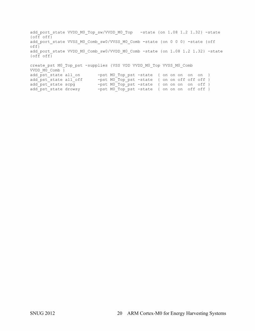
-control_port {ret M0/HEAD_RET[3]} -on_state {on_state VDD {ret}} #----------------------------------------- #M0 Combinational Logic VVSS Power Switch & Retention switch #----------------------------------------- create_power_switch VVSS_M0_Comb_sw0 -domain M0_Comb_PD -input_supply_port {VSS VSS} -output_supply_port {VVSS_M0_Comb VVSS_M0_Comb} \ -control_port {sleep M0/FOOT_SLEEP[0]} -on_state {on_state VSS {sleep}} create_power_switch VVSS_M0_Comb_sw1 -domain M0_Comb_PD -input_supply_port {VSS VSS} -output_supply_port {VVSS_M0_Comb VVSS_M0_Comb} \ -control_port {sleep M0/FOOT_SLEEP[1]} -on_state {on_state VSS {sleep}} create_power_switch VVSS_M0_Comb_sw2 -domain M0_Comb_PD -input_supply_port {VSS VSS} -output_supply_port {VVSS_M0_Comb VVSS_M0_Comb} \ -control_port {sleep M0/FOOT_SLEEP[2]} -on_state {on_state VSS {sleep}} create_power_switch VVSS_M0_Comb_sw3 -domain M0_Comb_PD -input_supply_port {VSS VSS} -output_supply_port {VVSS_M0_Comb VVSS_M0_Comb} \ -control_port {sleep M0/FOOT_SLEEP[3]} -on_state {on_state VSS {sleep}} create_power_switch VVSS_M0_Comb_ret0 -domain M0_Comb_PD -input_supply_port {VSS VSS} -output_supply_port {VVSS_M0_Comb VVSS_M0_Comb} \ -control_port {ret M0/FOOT_RET[0]} -on_state {on_state VSS {!ret}} create_power_switch VVSS_M0_Comb_ret1 -domain M0_Comb_PD -input_supply_port {VSS VSS} -output_supply_port {VVSS_M0_Comb VVSS_M0_Comb} \ -control_port {ret M0/FOOT_RET[1]} -on_state {on_state VSS {!ret}} create_power_switch VVSS_M0_Comb_ret2 -domain M0_Comb_PD -input_supply_port {VSS VSS} -output_supply_port {VVSS_M0_Comb VVSS_M0_Comb} \ -control_port {ret M0/FOOT_RET[2]} -on_state {on_state VSS {!ret}} create_power_switch VVSS_M0_Comb_ret3 -domain M0_Comb_PD -input_supply_port {VSS VSS} -output_supply_port {VVSS_M0_Comb VVSS_M0_Comb} \ -control_port {ret M0/FOOT_RET[3]} -on_state {on_state VSS {!ret}} #----------------------------------------- #M0 Comb Outputs Isolation Stategy #----------------------------------------- set_isolation M0_Comb_isol \ -domain M0_Comb_PD \ -isolation_power_net VVDD_M0_Top \ -isolation_ground_net VSS \ -clamp_value 0 set_isolation_control M0_Comb_isol \ -domain M0_Comb_PD \ -isolation_signal M0/ISOLATE \ -isolation_sense high \ -location parent set_isolation M0_Comb_noIso \ -domain M0_Comb_PD \ -elements M0/combinational/VIRTUALRAIL \ -no_isolation #----------------------------------------- #Port States #----------------------------------------- add_port_state VDD -state {on 1.08 1.2 1.32} add_port_state VSS -state {on 0 0 0}
SNUG 2012 20 ARM Cortex-M0 for Energy Harvesting Systems
add_port_state VVDD_M0_Top_sw/VVDD_M0_Top -state {on 1.08 1.2 1.32} -state {off off} add_port_state VVSS_M0_Comb_sw0/VVSS_M0_Comb -state {on 0 0 0} -state {off off} add_port_state VVDD_M0_Comb_sw0/VVDD_M0_Comb -state {on 1.08 1.2 1.32} -state {off off} create_pst M0_Top_pst -supplies {VSS VDD VVDD_M0_Top VVSS_M0_Comb VVDD_M0_Comb } add_pst_state all_on -pst M0_Top_pst -state { on on on on on } add_pst_state all_off -pst M0_Top_pst -state { on on off off off } add_pst_state scpg -pst M0_Top_pst -state { on on on on off } add_pst_state drowsy -pst M0_Top_pst -state { on on on off off }