amorphous silicon carbide photoelectrode for hydrogen...
TRANSCRIPT

15
Amorphous Silicon Carbide Photoelectrode for Hydrogen Production from Water using Sunlight
Feng Zhu1, Jian Hu1, Ilvydas Matulionis1, Todd Deutsch2, Nicolas Gaillard3, Eric Miller3, and Arun Madan1
1MVSystems, Inc., 500 Corporate Circle, Suite L, Golden, CO, 80401 2Hawaii Natural Energy Institute (HNEI), University of Hawaii at Manoa,
Honolulu, HI 96822, 3National Renewable Energy Laboratory (NREL), Golden, CO 80401,
USA
1. Introduction
Hydrogen is emerging as an alternative energy carrier to fossil fuels. There are many
advantages of hydrogen as a universal energy medium. For example, it is non-toxic and its
combustion with oxygen results in the formation of water to release energy. In this chapter,
we discuss the solar to hydrogen production directly from water using a
photoelectrochemical (PEC) cell; in particular we use amorphous silicon carbide (a-SiC:H) as
a photoelectrode integrated with a-Si tandem photovoltaic (PV) cell. High quality a-SiC:H
thin film with bandgap ≥2.0eV was fabricated by plasma enhanced chemical vapor
deposition (PECVD) technique using SiH4, H2 and CH4 gas mixture. Incorporation of carbon
in the a-SiH film not only increased the bandgap, but also led to improved corrosion
resistance to an aqueous electrolyte. Adding H2 during the fabrication of a-SiC:H material
could lead to a decrease of the density of states (DOS) in the film. Immersing the a-
SiC:H(p)/a-SiC:H(i) structure in an aqueous electrolyte showed excellent durability up to
100 hours (so far tested); in addition, the photocurrent increased and its onset shifted
anodically after 100-hour durability test. It was also found that a SiOx layer formed on the
surface of a-SiC:H, when exposed to air led to a decrease in the photocurrent and its onset
shifted cathodically; by removing the SiOx layer, the photocurrent increased and its onset
was driven anodically. Integrating with a-Si:H tandem cell, the flat-band potential of the
PV/a-SiC:H structure shifts significantly below the H2O/O2 half-reaction potential and is in
an appropriate position to facilitate water splitting and has exhibited encouraging results.
The PV/a-SiC:H structure produced hydrogen bubbles from water splitting and exhibited
good durability in an aqueous electrolyte for up to 150 hours (so far tested). In a two-
electrode setup (with ruthenium oxide as counter electrode), which is analogous to a real
PEC cell configuration, the PV/a-SiC:H produces photocurrent of about 1.3 mA/cm2 at zero
bias, which implies a solar-to-hydrogen (STH) conversion efficiency of over 1.6%. Finally,
we present simulation results which indicate that a-SiC:H as a photoelectrode in the PV/a-
SiC:H structure could lead to STH conversion efficiency of >10%. Source: Solar Energy, Book edited by: Radu D. Rugescu,
ISBN 978-953-307-052-0, pp. 432, February 2010, INTECH, Croatia, downloaded from SCIYO.COM
www.intechopen.com
Solar Energy
354
2. Principles and status of using semiconductor in PEC
In general, hydrogen can be obtained electrolytically, photo-electrochemically,
thermochemically, and biochemically by direct decomposition from the most abundant
material on earth: water. Though a hydrogen-oxygen fuel cell operates without generating
harmful emissions, most hydrogen production techniques such as direct electrolysis, steam-
methane reformation and thermo-chemical decomposition of water can give rise to
significant greenhouse gases and other harmful by-products. We will briefly review the
solid-state semiconductor electrodes for PEC water splitting using sunlight. Photochemical
hydrogen production is similar to a thermo-chemical system, in that it also employs a
system of chemical reactants, which leads to water splitting. However, the driving force is
not thermal energy but sunlight. In this sense, this system is similar to the photosynthetic
system present in green plants. In its simplest form, a photoelectrochemical (PEC) hydrogen
cell consists of a semiconductor as a reaction electrode (RE) and a metal counter electrode
(CE) immersed in an aqueous electrolyte, and PEC water splitting at the semiconductor-
electrolyte interface drove by sunlight, which is of considerable interest as it offers an
environmentally “green” and renewable approach to hydrogen production (Memming,
2000).
2.1 Principles of PEC The basic principles of semiconductor electrochemistry have been described in several
papers and books (Fujishima & Honda, 1972; Gerscher & Mindt, 1968; Narayanan &
Viswanathan, 1998; Memming, 2000; Gratzel, 2001).
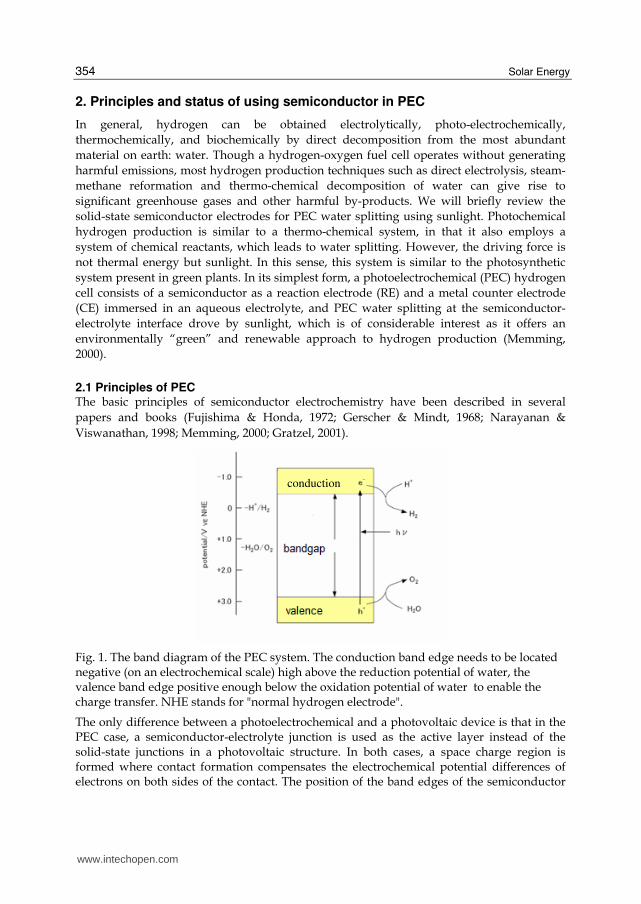
Fig. 1. The band diagram of the PEC system. The conduction band edge needs to be located negative (on an electrochemical scale) high above the reduction potential of water, the valence band edge positive enough below the oxidation potential of water to enable the charge transfer. NHE stands for "normal hydrogen electrode".
The only difference between a photoelectrochemical and a photovoltaic device is that in the PEC case, a semiconductor-electrolyte junction is used as the active layer instead of the solid-state junctions in a photovoltaic structure. In both cases, a space charge region is formed where contact formation compensates the electrochemical potential differences of electrons on both sides of the contact. The position of the band edges of the semiconductor
conduction
www.intechopen.com
Amorphous Silicon Carbide Photoelectrode for Hydrogen Production from Water using Sunlight
355
at the interface can be assumed in a first approximation to be dependent only on the pH of the solution and independent of the potential (Fermi level) of the electrode or the electrolyte (Memming, 2000; Kuznetsov & Ulstrup, 2000). For direct photoelectrochemical decomposition of water, several primary requirements of the semiconductor must be met: the semiconductor system must generate sufficient voltage (separation of the quasi Fermi levels under illumination) to drive the electrolysis, the energetic of the semiconductor must overlap that of the hydrogen and oxygen redox reactions (saying the band positions at the semiconductor-electrolyte interface have to be located at an energetically suitable position as shown in Fig.1), the semiconductor system must be stable in aqueous electrolytes, and finally the charge transfer from the surface of the semiconductor must be fast enough not only to prevent corrosion but also reduce energy losses due to overvoltage (Gerscher & Mindt, 1968; Narayanan & Viswanathan, 1998; Memming, 2000). Neglecting losses, the energy required to split water is 237.18 kJ/mol, which converts into 1.23 eV, i.e. the PV device must be able to generate more than 1.23 Volts. The STH conversion efficiency in PEC cells can be generally expressed as
Efficiency= =chemical energy in hydrogen produced in a PEC cell
energy in the sunlight over the collection area
ph Ws
S
J V
E (1)
where Jph is the photocurrent density (in mA/cm2) generated in a PEC cell, VWS = 1.23 V is the potential corresponding to the Gibbs free energy change per photon required to split water, and Es is the solar irradiance (in mW/cm2). Under AM1.5 G illumination, a simple approximation for the STH efficiency is Jph times 1.23(in %) (Memming, 2000; Miller & Rocheleau, 2002).
2.2 Status of using semiconductor in PEC Although as early as in 1839 E. Becquerel (Memming, 2000) had discovered the photovoltaic
effect by illuminating a platinum electrode covered with a silver halide in an electrochemical
cell, the foundation of modern photoelectrochemistry has been laid down much later by the
work of Brattain and Garret and subsequently Gerischer (Bak, et al., 2002; Mary & Arthru,
2008), who undertook the first detailed electrochemical and photoelectrochemical studies of
the semiconductor–electrolyte interface. From then on, various methods of water splitting
have been explored to improve the hydrogen production efficiency. So far, many materials
that could be used in the PEC cell structure have been identified as shown in Fig.2.
However, only a few of the common semiconductors can fulfil the requirements presented
above even if it is assumed that the necessary overvoltage is zero. It should be noted that
most materials have poor corrosion resistance in an aqueous electrolyte and posses high
bandgap, which prevents them from producing enough photocurrent (Fig.5).
Photoelectrolysis of water, first reported in the early 1970’s (Fujishima, 1972), has recently
received renewed interest since it offers a renewable, non-polluting approach to hydrogen
production. So far water splitting using sunlight has two main approaches. The first is a
two-step process, which means sunlight first transform into electricity which is then used to
split water for hydrogen production (Tamaura, et al., 1995; Hassan & Hartmut, 1998).
Though only about 2V is needed to split water, hydrogen production efficiency depends on
large current via wires, resulting in loss due to its resistance; the two-step process for
hydrogen production is complex and leads to a high cost.
www.intechopen.com

Solar Energy
356
Fig. 2. Band positions of some semiconductors in contact with aqueous electrolyte at pH1. The lower edge of the conduction band (red colour) and the upper edge of the valence band (green colour) are presented along with the bandgap in electron volts. For comparison, the vacuum energy scale as used in solid state physics and the electrochemical energy scales, with respect to a normal hydrogen electrode (NHE) as reference points, are shown as well as the standard potentials of several redox couples are presented against the standard hydrogen electrode potential on the right side (Gratzel, 2001).
Another approach is a one-step process, in which there are no conductive wires and all the parts are integrated for water splitting, as shown in Fig.3. In this structure as there are no wires, hence no loss. Another advantage is that the maintenance is low compared to the two-step process discussed above.
Fig. 3. Generic Planar Photoelectrode Structure with Hydrogen and Oxygen Evolved at Opposite Surfaces (Miller & Rocheleau, 2002)
In 1972, Fujishima and Honda used n type TiO2 as the anode and Pt as the cathode to form the PEC structure and achieved 0.1% of STH efficiency (Fujishima & Honda, 1972). In this system TiO2 absorbed the sunlight to produce the current while its bandgap (~3.2eV) provided the needed voltage for water splitting. Although TiO2 is corrosion resistant in an aqueous electrolyte, but because of its high band gap leads to absorption of sunlight in the
www.intechopen.com

Amorphous Silicon Carbide Photoelectrode for Hydrogen Production from Water using Sunlight
357
short wavelength range only, resulting in a small current and hence a low STH efficiency. In order to increase the current, some researchers are attempting to narrow its bandgap to enhance its absorption, and with limited success (Masayoshi, et al., 2005; Nelson & Thomas, 2005; Srivastava, et al. 2000). In 1975, Nozik first reported using SrTiO3(n) and GaP(p) photoelectrodes as the anode and cathode respectively (Nozik, 1975) and obtained a STH efficiency of 0.67%. In 1976, Morisaki’s group introduced utilizing a solar cell to assist the PEC process for hydrogen production (Morisaki, et al., 1976). Silicon solar cell was integrated with TiO2 in series to form a PEC system, which exhibited higher photo current by absorbing more sunlight and higher voltage. Later, Khaselev and Turner in 1998 reported 12.4% of STH efficiency using p-GaInP2/n–GaAs/p-GaAs/Pt structure (Khaselev & Turner, 1998); in this, surface oxygen was produced at the p-GaInP2 side and hydrogen from the Pt side. Although this structure exhibited high STH efficiency, the corrosion resistance of p-GaInP2 in an aqueous electrolytes was very poor, and was almost all etched away within a couple of hours. (Deutsch et al., 2008).
Fig. 4. (a) A-Si triple PV junctions and (b) CIGS PV cell integrated into a PEC system (Miller, et al., 2003)
Richard et al., reported 7.8% of STH efficiency by using NiMo or CoMo as cathode, Ni-Fe-O metal as anode and integrating with a-Si/a-Si:Ge/a-Si:Ge triple junctions solar cell as shown in Fig.4 (a) (Richard, et al., 1998). They also used copper indium gallium selenide (CIGS) module to replace a-Si triple junctions to produce even higher photo current as shown in Fig.4 (b). Yamada, et al., also used a similar structure (Co–Mo and the Fe–Ni–O as the electrodes) and achieved 2.5% STH efficiency (Yamada, et al., 2003). More notably, a STH efficiency of 8% was reported by Lichta, et al., using AlGaAs/Si RuO2/Pt black structure (Lichta, et al., 2001). In this structure, solar cell was separated from the aqueous electrolyte to avoid being corroded; it should be noted that the fabrication process for the device was very complicated. The non-transparent electrode had to cover the active area of the solar cell in order to enlarge electrode-electrolyte contact to as large area as possible. In 2006, a “hybrid” PEC device consisting of substrate/amorphous silicon (nipnip)/ ZnO/WO3, which would lead to ~3% solar-to-hydrogen (STH) conversion efficiency, was reported (Stavrides, et al., 2006). In this configuration, transparent WO3 prepared by sputtering technique acted as the photoelectrode, whereas the amorphous silicon tandem solar cell was used as a photovoltaic device to provide additional voltage for water splitting at the interface of photoelectrode-electrolyte. In this structure, primarily the UV photons are absorbed by WO3 while the green to red portion of the AM1.5 Global spectra was absorbed in the a-Si tandem photovoltaic device. Due to a high bandgap (Eg) (2.6-2.8eV) of the WO3 photoelectrode, the photocurrent density of this hybrid PEC device is limited to no more than 5 mA/cm2 (as shown in Fig.5), resulting in low STH efficiency.
www.intechopen.com
Solar Energy
358
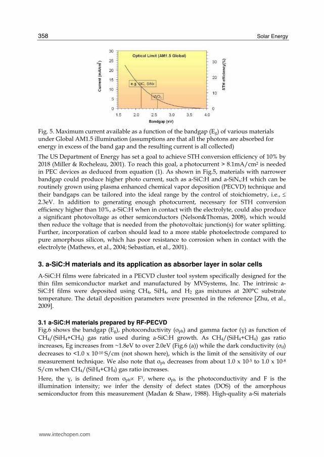
Fig. 5. Maximum current available as a function of the bandgap (Eg) of various materials under Global AM1.5 illumination (assumptions are that all the photons are absorbed for energy in excess of the band gap and the resulting current is all collected)
The US Department of Energy has set a goal to achieve STH conversion efficiency of 10% by 2018 (Miller & Rocheleau, 2001). To reach this goal, a photocurrent > 8.1mA/cm2 is needed in PEC devices as deduced from equation (1). As shown in Fig.5, materials with narrower bandgap could produce higher photo current, such as a-SiC:H and a-SiNx:H which can be routinely grown using plasma enhanced chemical vapor deposition (PECVD) technique and
their bandgaps can be tailored into the ideal range by the control of stoichiometry, i.e., ≤ 2.3eV. In addition to generating enough photocurrent, necessary for STH conversion efficiency higher than 10%, a-SiC:H when in contact with the electrolyte, could also produce a significant photovoltage as other semiconductors (Nelson&Thomas, 2008), which would then reduce the voltage that is needed from the photovoltaic junction(s) for water splitting. Further, incorporation of carbon should lead to a more stable photoelectrode compared to pure amorphous silicon, which has poor resistance to corrosion when in contact with the electrolyte (Mathews, et al., 2004; Sebastian, et al., 2001).
3. a-SiC:H materials and its application as absorber layer in solar cells
A-SiC:H films were fabricated in a PECVD cluster tool system specifically designed for the thin film semiconductor market and manufactured by MVSystems, Inc. The intrinsic a-SiC:H films were deposited using CH4, SiH4, and H2 gas mixtures at 200°C substrate temperature. The detail deposition parameters were presented in the reference [Zhu, et al., 2009].
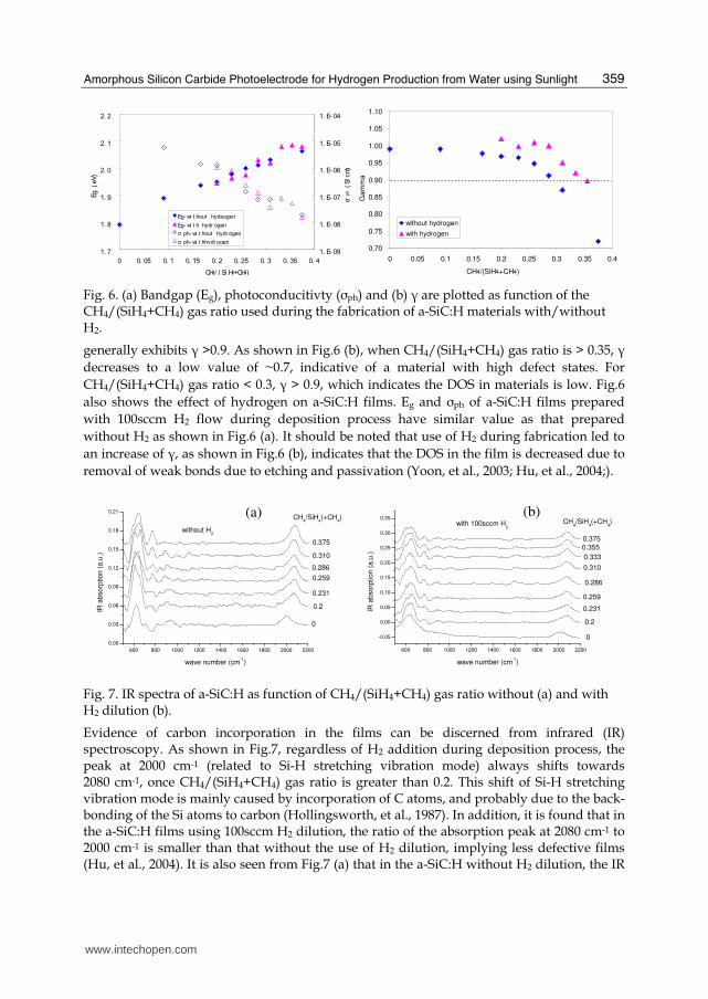
3.1 a-SiC:H materials prepared by RF-PECVD Fig.6 shows the bandgap (Eg), photoconductivity (σph) and gamma factor (γ) as function of
CH4/(SiH4+CH4) gas ratio used during a-SiC:H growth. As CH4/(SiH4+CH4) gas ratio
increases, Eg increases from ~1.8eV to over 2.0eV (Fig.6 (a)) while the dark conductivity (σd)
decreases to <1.0 x 10⁻¹⁰ S/cm (not shown here), which is the limit of the sensitivity of our
measurement technique. We also note that σph decreases from about 1.0 x 10⁻⁵ to 1.0 x 10⁻⁸
S/cm when CH4/(SiH4+CH4) gas ratio increases.
Here, the γ, is defined from σph∝ Fγ, where σph is the photoconductivity and F is the illumination intensity; we infer the density of defect states (DOS) of the amorphous semiconductor from this measurement (Madan & Shaw, 1988). High-quality a-Si materials
www.intechopen.com
Amorphous Silicon Carbide Photoelectrode for Hydrogen Production from Water using Sunlight
359
1. 7
1. 8
1. 9
2. 0
2. 1
2. 2
0 0. 05 0. 1 0. 15 0. 2 0. 25 0. 3 0. 35 0. 4CH4/ ( Si H4+CH4)
Eg (
eV)
1. E- 09
1. E- 08
1. E- 07
1. E- 06
1. E- 05
1. E- 04
σph
(S/
cm)
Eg- wi t hout hydeogenEg- wi t h hydr ogenσ ph- wi t hout hydr ogenσ ph- wi t hhydr ogen
0.70
0.75
0.80
0.85
0.90
0.95
1.00
1.05
1.10
0 0.05 0.1 0.15 0.2 0.25 0.3 0.35 0.4
CH4/(SiH4+CH4)
Gam
ma
without hydrogen
with hydrogen
Fig. 6. (a) Bandgap (Eg), photoconducitivty (σph) and (b) γ are plotted as function of the CH4/(SiH4+CH4) gas ratio used during the fabrication of a-SiC:H materials with/without H2.
generally exhibits γ >0.9. As shown in Fig.6 (b), when CH4/(SiH4+CH4) gas ratio is > 0.35, γ
decreases to a low value of ~0.7, indicative of a material with high defect states. For
CH4/(SiH4+CH4) gas ratio < 0.3, γ > 0.9, which indicates the DOS in materials is low. Fig.6
also shows the effect of hydrogen on a-SiC:H films. Eg and σph of a-SiC:H films prepared
with 100sccm H2 flow during deposition process have similar value as that prepared
without H2 as shown in Fig.6 (a). It should be noted that use of H2 during fabrication led to
an increase of γ, as shown in Fig.6 (b), indicates that the DOS in the film is decreased due to
removal of weak bonds due to etching and passivation (Yoon, et al., 2003; Hu, et al., 2004;).
600 800 1000 1200 1400 1600 1800 2000 2200
0.00
0.03
0.06
0.09
0.12
0.15
0.18
0.21CH
4/SiH
4(+CH
4)
without H2
0.375
0.310
0.286
0.259
0.231
0.2
0
IR a
bsorp
tion (
a.u
.)
wave number (cm-1)
600 800 1000 1200 1400 1600 1800 2000 2200
-0.05
0.00
0.05
0.10
0.15
0.20
0.25
0.30
0.35
0
with 100sccm H2
0.2
0.375
0.355
0.333
0.310
0.286
0.231
CH4/SiH
4(+CH
4)
0.259
IR a
bsorp
tion (
a.u
.)
wave number (cm-1)
Fig. 7. IR spectra of a-SiC:H as function of CH4/(SiH4+CH4) gas ratio without (a) and with H2 dilution (b).
Evidence of carbon incorporation in the films can be discerned from infrared (IR) spectroscopy. As shown in Fig.7, regardless of H2 addition during deposition process, the peak at 2000 cm-1 (related to Si-H stretching vibration mode) always shifts towards 2080 cm-1, once CH4/(SiH4+CH4) gas ratio is greater than 0.2. This shift of Si-H stretching vibration mode is mainly caused by incorporation of C atoms, and probably due to the back-bonding of the Si atoms to carbon (Hollingsworth, et al., 1987). In addition, it is found that in the a-SiC:H films using 100sccm H2 dilution, the ratio of the absorption peak at 2080 cm-1 to 2000 cm-1 is smaller than that without the use of H2 dilution, implying less defective films (Hu, et al., 2004). It is also seen from Fig.7 (a) that in the a-SiC:H without H2 dilution, the IR
(a) (b)
www.intechopen.com

Solar Energy
360
peak at 780 cm-1, which is related to Si-C stretching mode, increases as the CH4/(SiH4+CH4) gas ratio increases; whereas films produced with 100sccm H2 dilution, this peak keeps almost constant (as shown Fig.7(b)). This is likely due to the removal of SiH2 and a decrease of carbon clusters in the films (Desalvo, et al., 1997). It was also found that at a fixed CH4/(SiH4+CH4) =0.2, σph is enhanced from 4.0 x 10⁻⁷ S/cm to 3.2 x 10⁻⁶ S/cm as the H2 flow increased from 0 to 150sccm. The decrease in σph with increasing CH4/(SiH4+CH4) gas ratio as shown in Fig. 6(a) is unlikely be due to an increase of the recombination centers related to defects since the γ factor is >0.9.The decrease of σph results from a reduction in the absorption coefficient as Eg increases. In order to further evaluate this, the nominal photocurrent, Ip, at certain wavelength, under uniform bulk absorption (here we select wavelength 600nm) can be measured and the photocurrent be expressed as,
Ip = e.Nph (λ) (1-Rλ) [1 – exp ( –αλ d)]ηĩ/tt (2)
Where, Nph(λ) is the photon flux, Rλ is the reflection coefficient, αλ the absorption coefficient, d the film thickness, η is the quantum efficiency of photo generation, ĩ is the recombination lifetime and tt is the transit time. Assuming that η, ĩ, tt and (1-Rλ) are constant for different films (i.e. different Eg), then to the first order approximation, the normalized photocurrent,
Ip/[1– exp(–αλd)], can account for the changes in the absorption coefficient as Eg varies (Madan & Shaw, 1988). It was indeed shown that the normalized photocurrent does not change significantly as Eg increases (Hu, et al., 2008). This is in contrast to the decrease in σph with Eg as shown in Fig.6 (a), suggesting a low DOS, consistent with high γ (>0.9) throughout the range.
3.2 Photothermal deflection spectroscopy (PDS) spectrum of a-SiC:H films
Fig. 8. Absorption coefficient curves of three a-SiC:H films, with differing carbon concentrations, measured using photothermal deflection spectroscopy (PDS)
Fig.8 shows the absorption coefficient of the three chosen films with differing carbon
concentrations, prepared with H2 dilution, measured by the photothermal deflection
www.intechopen.com
Amorphous Silicon Carbide Photoelectrode for Hydrogen Production from Water using Sunlight
361
spectroscopy (PDS). Using energy dispersive x-ray spectroscopy on a JEOL JSM-7000F field
emission scanning electron microscope with an EDAX Genesis energy dispersive x-ray
spectrometer their carbon concentrations are 6, 9, and 11% (in atomic), corresponding to
methane gas ratio, used in the fabrication, of 0.20, 0.29 and 0.33 respectively. The signal seen
here is a convolution of optical absorption from every possible electronic region including
extended, localized and deep defect states. In the linear region between about 1.7–2.1eV, the
absorption coefficient primarily results from localized to extended state transitions and is
known as the Urbach tail. This region can be described by α=α0 exp(E/E0) where E is the
excitation energy and E0 is the Urbach energy which is the inverse slope of the data when
plotted versus ln(α). Since the absorption coefficient here directly depends on the density of
localized states, E0 is considered to be a measure of the amount of disorder (Cody, et al.,
1981). Their bandgap values are presented in Fig.6 (a) as previously discussed and E0 is 78,
85, and 98 meV for carbon concentrations of 6, 9, and 11%, respectively. For comparison, a
typical value for device grade a-Si:H is ~50 meV(Madan & Shaw, 1988). As the carbon
concentration increases, so too does the value of E0. This is expected as the density of
localized states is increasing with more disorder created by introducing more carbon. Also,
there is an increase in the bandgap from E04 = 2.06-2.18eV with carbon concentration (E04 is
defined as the energy value where the absorption coefficient α = 104 cm-1). This is known to
be a result of at least some of the carbon being incorporated in the form of sp3 carbon which
is essentially an insulator (Solomon, 2001). The feature at 0.88eV in Fig. 8 is an overtone of
an O-H vibrational stretch mode from the quartz substrate.
As the bandgap increases with carbon incorporation, as evidenced from the PDS data, the Urbach energies are 50% to 100% higher than is typically seen in device grade a-Si:H. This is typically interpreted as an increase in localized states within the bandgap region just above the valence band and below the conduction band resulting from structural disorder. It is believed that the carbon is incorporated into our films as a mixture of sp2 and sp3 carbon from ESR test (Solomon, 2001; Simonds (a), et al., 2009).
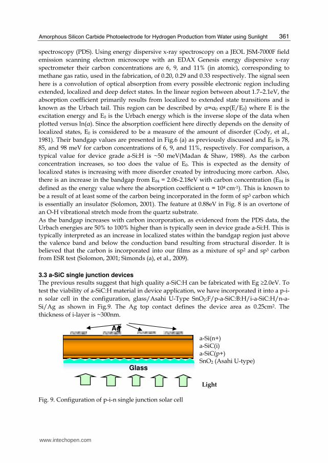
3.3 a-SiC single junction devices
The previous results suggest that high quality a-SiC:H can be fabricated with Eg ≥2.0eV. To
test the viability of a-SiC:H material in device application, we have incorporated it into a p-i-
n solar cell in the configuration, glass/Asahi U-Type SnO2:F/p-a-SiC:B:H/i-a-SiC:H/n-a-
Si/Ag as shown in Fig.9. The Ag top contact defines the device area as 0.25cm2. The
thickness of i-layer is ~300nm.
Fig. 9. Configuration of p-i-n single junction solar cell
Glass
a-Si(n+) a-SiC(i) a-SiC(p+) SnO2 (Asahi U-type)
Light
Ag
www.intechopen.com
Solar Energy
362
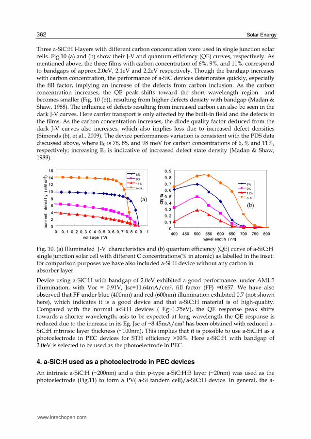
Three a-SiC:H i-layers with different carbon concentration were used in single junction solar cells. Fig.10 (a) and (b) show their J-V and quantum efficiency (QE) curves, respectively. As mentioned above, the three films with carbon concentration of 6%, 9%, and 11%, correspond to bandgaps of approx.2.0eV, 2.1eV and 2.2eV respectively. Though the bandgap increases with carbon concentration, the performance of a-SiC devices deteriorates quickly, especially the fill factor, implying an increase of the defects from carbon inclusion. As the carbon concentration increases, the QE peak shifts toward the short wavelength region and becomes smaller (Fig. 10 (b)), resulting from higher defects density with bandgap (Madan & Shaw, 1988). The influence of defects resulting from increased carbon can also be seen in the dark J-V curves. Here carrier transport is only affected by the built-in field and the defects in the films. As the carbon concentration increases, the diode quality factor deduced from the dark J-V curves also increases, which also implies loss due to increased defect densities (Simonds (b), et al., 2009). The device performances variation is consistent with the PDS data discussed above, where E0 is 78, 85, and 98 meV for carbon concentrations of 6, 9, and 11%, respectively; increasing E0 is indicative of increased defect state density (Madan & Shaw, 1988).
0
24
68
10
1214
16
0 0. 1 0. 2 0. 3 0. 4 0. 5 0. 6 0. 7 0. 8 0. 9 1vol t age ( V)
curr
ent
dens
ity
(mA/
cm2 ) 6%
9%11%a- Si
00. 10. 20. 30. 40. 50. 60. 70. 80. 9
400 450 500 550 600 650 700 750 800wavel engt h ( nm)
QE(%
)
6%9%11%a- Si
Fig. 10. (a) Illuminated J-V characteristics and (b) quantum efficiency (QE) curve of a-SiC:H single junction solar cell with different C concentrations(% in atomic) as labelled in the inset: for comparison purposes we have also included a-Si H device without any carbon in absorber layer.
Device using a-SiC:H with bandgap of 2.0eV exhibited a good performance. under AM1.5 illumination, with Voc = 0.91V, Jsc=11.64mA/cm2, fill factor (FF) =0.657. We have also observed that FF under blue (400nm) and red (600nm) illumination exhibited 0.7 (not shown here), which indicates it is a good device and that a-SiC:H material is of high-quality. Compared with the normal a-Si:H devices ( Eg~1.75eV), the QE response peak shifts towards a shorter wavelength; asis to be expected at long wavelength the QE response is reduced due to the increase in its Eg. Jsc of ~8.45mA/cm2 has been obtained with reduced a-SiC:H intrinsic layer thickness (~100nm). This implies that it is possible to use a-SiC:H as a photoelectrode in PEC devices for STH efficiency >10%. Here a-SiC:H with bandgap of 2.0eV is selected to be used as the photoelectrode in PEC.
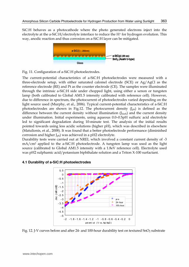
4. a-SiC:H used as a photoelectrode in PEC devices
An intrinsic a-SiC:H (~200nm) and a thin p-type a-SiC:H:B layer (~20nm) was used as the photoelectrode (Fig.11) to form a PV( a-Si tandem cell)/a-SiC:H device. In general, the a-
(a)(b)
www.intechopen.com
Amorphous Silicon Carbide Photoelectrode for Hydrogen Production from Water using Sunlight
363
SiC:H behaves as a photocathode where the photo generated electrons inject into the electrolyte at the a-SiC:H/electrolyte interface to reduce the H+ for hydrogen evolution. This way, anodic reaction and thus corrosion on a-SiC:H layer can be mitigated.
a-SiC(p) (20 nm)
SnO2 (Asahi U-type)
Glass
a-SiC(i) (~200nm)
a-SiC(p) (20 nm)
SnO2 (Asahi U-type)
Glass
a-SiC(i) (~200nm)
Fig. 11. Configuration of a-SiC:H photoelectrodes.
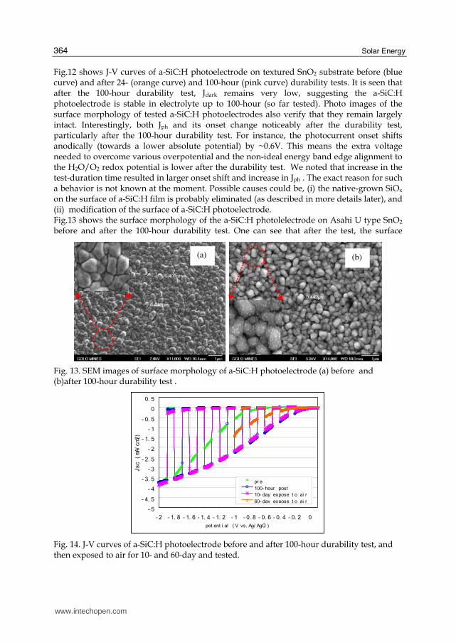
The current-potential characteristics of a-SiC:H photoelectrodes were measured with a three-electrode setup, with either saturated calomel electrode (SCE) or Ag/AgCl as the reference electrode (RE) and Pt as the counter electrode (CE). The samples were illuminated through the intrinsic a-SiC:H side under chopped light, using either a xenon or tungsten lamp (both calibrated to Global AM1.5 intensity calibrated with reference cell). However, due to difference in spectrum, the photocurrent of photoelectrodes varied depending on the light source used (Murphy, et al., 2006). Typical current-potential characteristics of a-SiC:H photoelectrodes are shown in Fig.12. The photocurrent density (Jph) is defined as the difference between the current density without illumination (Jdark) and the current density under illumination. Initial experiments, using aqueous 0.0–0.5pH sulfuric acid electrolyte led to significant degradation during 10-minute test. The analysis of the initial results pointed towards using less acidic solutions (higher pH), which was described in elsewhere (Matulionis, et al., 2008). It was found that a better photoelectrode performance (diminished corrosion and higher Jph) was achieved in a pH2 electrolyte. Durability tests were carried out at NREL which involved a constant current density of -3 mA/cm2 applied to the a-SiC:H photoelectrode. A tungsten lamp was used as the light source (calibrated to Global AM1.5 intensity with a 1.8eV reference cell). Electrolyte used was pH2 sulphamic acid/potassium biphthalate solution and a Triton X-100 surfactant.
4.1 Durability of a-SiC:H photoelectrodes
- 5- 4. 5
- 4- 3. 5
- 3- 2. 5
- 2- 1. 5
- 1- 0. 5
00. 5
- 2 - 1. 8 - 1. 6 - 1. 4 - 1. 2 - 1 - 0. 8 - 0. 6 - 0. 4 - 0. 2 0pot ent i al ( V vs. Ag/ AgCl )
Jsc
(mA/
cm2)
pr e24- hour100- hour
Fig. 12. J-V curves before and after 24- and 100-hour durability test on textured SnO2 substrate
www.intechopen.com
Solar Energy
364
Fig.12 shows J-V curves of a-SiC:H photoelectrode on textured SnO2 substrate before (blue curve) and after 24- (orange curve) and 100-hour (pink curve) durability tests. It is seen that after the 100-hour durability test, Jdark remains very low, suggesting the a-SiC:H photoelectrode is stable in electrolyte up to 100-hour (so far tested). Photo images of the surface morphology of tested a-SiC:H photoelectrodes also verify that they remain largely intact. Interestingly, both Jph and its onset change noticeably after the durability test, particularly after the 100-hour durability test. For instance, the photocurrent onset shifts anodically (towards a lower absolute potential) by ~0.6V. This means the extra voltage needed to overcome various overpotential and the non-ideal energy band edge alignment to the H2O/O2 redox potential is lower after the durability test. We noted that increase in the test-duration time resulted in larger onset shift and increase in Jph . The exact reason for such a behavior is not known at the moment. Possible causes could be, (i) the native-grown SiOx on the surface of a-SiC:H film is probably eliminated (as described in more details later), and (ii) modification of the surface of a-SiC:H photoelectrode. Fig.13 shows the surface morphology of the a-SiC:H photolelectrode on Asahi U type SnO2 before and after the 100-hour durability test. One can see that after the test, the surface
Fig. 13. SEM images of surface morphology of a-SiC:H photoelectrode (a) before and (b)after 100-hour durability test .
- 5- 4. 5
- 4- 3. 5
- 3- 2. 5
- 2- 1. 5
- 1- 0. 5
00. 5
- 2 - 1. 8 - 1. 6 - 1. 4 - 1. 2 - 1 - 0. 8 - 0. 6 - 0. 4 - 0. 2 0pot ent i al ( V vs. Ag/ AgCl )
Jsc
(mA/
cm2)
pr e100- hour post10- day expose t o ai r60- day expose t o ai r
Fig. 14. J-V curves of a-SiC:H photoelectrode before and after 100-hour durability test, and then exposed to air for 10- and 60-day and tested.
(a) (b)
www.intechopen.com

Amorphous Silicon Carbide Photoelectrode for Hydrogen Production from Water using Sunlight
365
morphology of a-SiC:H looks similar. The only difference is that after the test there are many tiny motes on the surface of a-SiC:H photoelectrode and it appears as if something deposited on it as shown the insert magnified image in Fig.13(b), while before the test the surface is smooth (insert magnified image in Fig.13.(a)). More work is needed to understand this. We have also noted changes, in the J-V characteristic after the 100-hour test, a-SiC:H photoelectrode when exposed to air as shown in Fig.14. We note that after 10-day exposure to air, J-V characteristic remains unchanged. After exposing to air for 60 days Jph decreases and photocurrent onset shifts cathodically. The reason probably is that extended exposure to air could leads to SiOx formation on the surface of a-SiC:H photoelectrodes and its thickness could be time dependent.
4.2 Effect of SiOx on the surface of a-SiC:H As seen in Fig.12 and 14, the Jph and its onset of a-SiC:H photoelectrodes could vary under different conditions. As discussed above, there is a possibility of SiOx layer formation on the surface of a-SiC:H photoelectrodes. Using X-ray photoelectron spectroscopy (XPS), we have investigated the surface of a-SiC:H films. Fig.15 shows the XPS spectra for an a-SiC:H film conditions of “as-is” and after etching with hydrofluoric acid (HF concentration of 48%) for different etching times, 10 to 60 seconds. It is clearly seen that there is a very thin SiOx (a few nm thick) which exists on the a-SiC:H surface, as evident by the peak around 104eV which is associated with the Si-O bonds in SiOx. The SiOx layer becomes thinner as the HF etching time become longer, and disappears eventually after an HF dip for 30 seconds. The peak around 101eV related to Si peak, remains the same.
Fig. 15. Changes in XPS (a) and XES (b) curves of a-SiC:H films with HF etching of surface.
The XES curves of before and after HF dip are completely superimposed, which suggests that HF dip does not change the composition of a-SiC:H, as shown in Fig. 15(b). XES curves of crystal SiC wafer, Si wafer and SiO2 are also shown in Fig. 15 (b) as well as that of a-SiC:H. Crystal SiC wafer has characteristic peaks at 91eV and 98eV while crystal Si wafer exhibits peaks at 90eV and 92eV. One can see that the data for a-SiC:H curve includes crystal Si and SiC characteristic peaks but not SiO peaks which would be at 87eV and 95eV a-SiC:H.
www.intechopen.com
Solar Energy
366
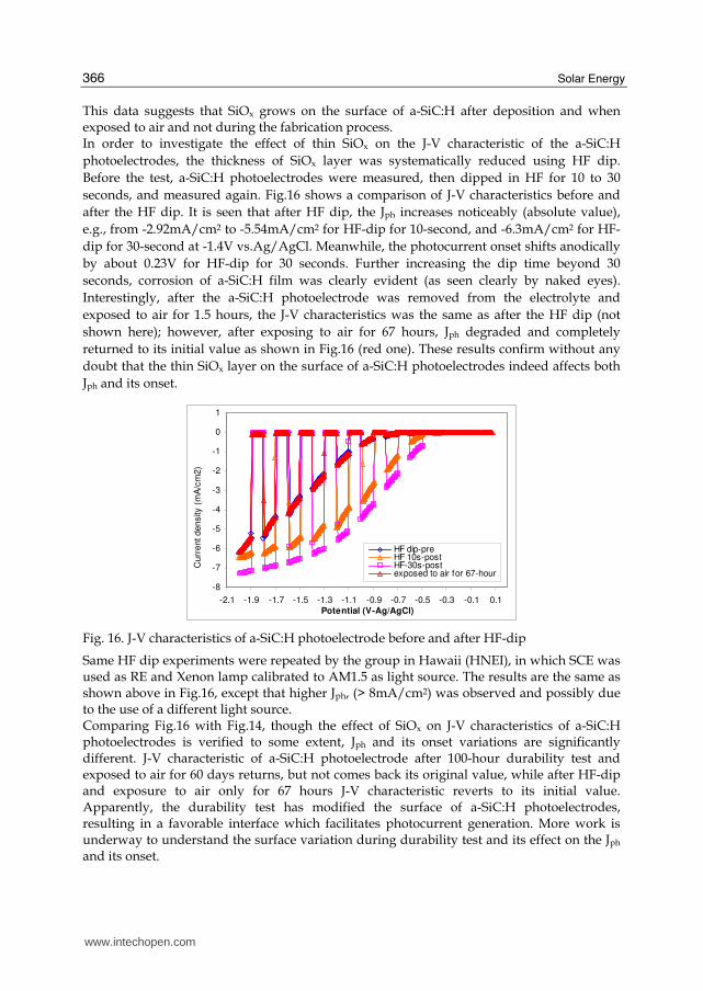
This data suggests that SiOx grows on the surface of a-SiC:H after deposition and when exposed to air and not during the fabrication process. In order to investigate the effect of thin SiOx on the J-V characteristic of the a-SiC:H
photoelectrodes, the thickness of SiOx layer was systematically reduced using HF dip.
Before the test, a-SiC:H photoelectrodes were measured, then dipped in HF for 10 to 30
seconds, and measured again. Fig.16 shows a comparison of J-V characteristics before and
after the HF dip. It is seen that after HF dip, the Jph increases noticeably (absolute value),
e.g., from -2.92mA/cm2 to -5.54mA/cm2 for HF-dip for 10-second, and -6.3mA/cm2 for HF-
dip for 30-second at -1.4V vs.Ag/AgCl. Meanwhile, the photocurrent onset shifts anodically
by about 0.23V for HF-dip for 30 seconds. Further increasing the dip time beyond 30
seconds, corrosion of a-SiC:H film was clearly evident (as seen clearly by naked eyes).
Interestingly, after the a-SiC:H photoelectrode was removed from the electrolyte and
exposed to air for 1.5 hours, the J-V characteristics was the same as after the HF dip (not
shown here); however, after exposing to air for 67 hours, Jph degraded and completely
returned to its initial value as shown in Fig.16 (red one). These results confirm without any
doubt that the thin SiOx layer on the surface of a-SiC:H photoelectrodes indeed affects both
Jph and its onset.
-8
-7
-6
-5
-4
-3
-2
-1
0
1
-2.1 -1.9 -1.7 -1.5 -1.3 -1.1 -0.9 -0.7 -0.5 -0.3 -0.1 0.1
Potential (V-Ag/AgCl)
Curr
ent density
(m
A/c
m2)
HF dip-preHF 10s-postHF-30s-postexposed to air for 67-hour
Fig. 16. J-V characteristics of a-SiC:H photoelectrode before and after HF-dip
Same HF dip experiments were repeated by the group in Hawaii (HNEI), in which SCE was used as RE and Xenon lamp calibrated to AM1.5 as light source. The results are the same as shown above in Fig.16, except that higher Jph, (> 8mA/cm2) was observed and possibly due to the use of a different light source. Comparing Fig.16 with Fig.14, though the effect of SiOx on J-V characteristics of a-SiC:H photoelectrodes is verified to some extent, Jph and its onset variations are significantly different. J-V characteristic of a-SiC:H photoelectrode after 100-hour durability test and exposed to air for 60 days returns, but not comes back its original value, while after HF-dip and exposure to air only for 67 hours J-V characteristic reverts to its initial value. Apparently, the durability test has modified the surface of a-SiC:H photoelectrodes, resulting in a favorable interface which facilitates photocurrent generation. More work is underway to understand the surface variation during durability test and its effect on the Jph and its onset.
www.intechopen.com

Amorphous Silicon Carbide Photoelectrode for Hydrogen Production from Water using Sunlight
367
4.3 Integration of the a-SiC:H photoelectrode with a-Si tandem device The above results show that the a-SiC:H photoelectrode exhibits high photocurrent (i.e., up to ~8 mA/cm2), and good durability in a pH2 electrolyte for up to ~100 hours. Its main drawback, however, is the non-ideal surface band structure. Our theoretical analysis showed that the hydrogen evolution reaction is thermodynamically allowed at the surface of the a-SiC:H photoelectrode, since the photogenerated electrons are of energy which is higher than the redox potential of H+/H2 half-reaction. On the other hand, to promote oxygen evolution at the counter electrode, a minimum external bias of ~ -1.4 V is needed to bring the quasi-Fermi energy level of photogenerated holes below H2O/O2 redox potential (Hu, et al., 2008). In order to solve this non-ideal valence band edge alignment problem, an a-Si:H tandem solar cell was integrated into the PEC cell to form a hybrid PV/a-SiC:H configuration, as shown in Figure 17(a). The substrate used for the hybrid PEC device was typically Asahi U-type fluorine-doped SnO2 coated glass. Other types of substrates such as stainless steel and ZnO coated glass were also used for comparison purposes. The a-Si:H tandem solar cell which was used in the hybrid PEC device when fabricated into a solid state device exhibited Voc = 1.71 V, Jsc=7.02 mA/cm2, FF=0.74, and efficiency of ~9%, as shown in Figure 17(b).
a-SiC(i)
light
a-SiC(p)
a-Si p-i-n
(top cell)
a-Si p-i-n
(bottom cell)
a-SiC(p)
a-Si(n)
a-SiC(p)
a-Si(n)
a-Si(i)
a-SiC p-i
a-Si(i)
Substrate
a-SiC(i)
light
a-SiC(p)
a-Si p-i-n
(top cell)
a-Si p-i-n
(bottom cell)
a-SiC(p)
a-Si(n)
a-SiC(p)
a-Si(n)
a-Si(i)
a-SiC p-i
a-Si(i)
Substrate
0
1
2
3
4
5
6
7
8
9
0.0 0.5 1.0 1.5 2.0
Voltage (V)
Curr
ent density (m
A/c
m2)
Voc = 1.712 V
Jsc = 7.02 mA/cm2
FF = 0.74
Efficiency = 8.89%
Fig. 17. (a) Configuration of the hybrid PEC device and (b) J-V curve of a-Si tandem device
4.4. Flat-band potential
-1.5
-1
-0.5
0
0.5
1
1.5
2
2.5-1 4 9 14
pH
V v
s. A
g/A
gC
l hydrogen
oxygen
a-SiC p- i
hybriddevice
Fig. 18. Vfb vs. pH for the a-SiC:H photoelectrode and the hybrid PEC device
www.intechopen.com

Solar Energy
368
Fig.18 shows the flat-band potential (Vfb), determined by the illuminated open-circuit potential (OCP) method, as a function of pH of electrolyte for both the a-SiC:H photoelectrode (open circles) and the hybrid PEC device (open triangles). The change of the Vfb with pH nearly exhibits a slope of ~60 mV/pH, as predicted by the Nernst equation (Memming, 2000). We note in Fig. 18, that at pH2, Vfb =+0.26 V (vs. Ag/AgCl) for the a-SiC:H photoelectrode, whereas in the case of the hybrid device, the Vfb significantly by ~ +1.6 V (as indicated by the red arrow) and is below the H2O/O2 half-reaction potential (by +0.97 V) and is in an appropriate position to facilitate water splitting. Figs.19 (a) and (b) show the current density vs. potential characteristics for hybrid PEC device fabricated on different substrates, SnO2 and ZnO coated glass and SS, and measured in the pH2 buffered electrolyte (sulphamic acid solution with added potassium biphthalate) using the 3-electrode and 2-electrode setup respectively. In the 2-electrode setup, there was no reference electrode and contained only the working electrode (hybrid PEC device) and the counter electrode which was ruthenium oxide (RuO2) rather than conventional platinum (Pt).
-5.0
-4.0
-3.0
-2.0
-1.0
0.0
-2.0 -1.5 -1.0 -0.5 0.0 0.5
Potential (V vs SCE)
Cu
rre
nt
de
ns
ity
(m
A/c
m2) SnO2 #1
SnO2 #2
SnO2 #3
ZnO
SS #1
SS #2
-5.0
-4.0
-3.0
-2.0
-1.0
0.0
-2.5 -2.0 -1.5 -1.0 -0.5 0.0 0.5
Potential (V)
Cu
rre
nt
de
ns
ity
(m
A/c
m2)
SnO2 #1
SnO2 #2
SnO2 #3
ZnO
SS #1
SS #2
Fig. 19. Current density vs. potential characteristics measured in (a) 3-electrode and (b) 2-electrode setup.
From Fig.19 (a), we see the saturated photocurrent of the hybrid cell using different substrates is in the range of 3-5 mA/cm2. The larger photocurrent using SnO2 (>4 mA/cm2) coated glass substrate is due to the inherent texture of the SnO2 which enhances internal photon absorption. More significantly, we see that the photocurrent density of ~0.3 mA/cm2 occurs at a zero potential using the 2-electrode setup (Fig.19 (b)). Hydrogen production was observed in a short-circuit condition (Hu, et al., 2009). It should be noted that compared with the 3-electrode case the photocurrent measured in the 2-electrode setup (even using RuO2 counter electrode) is much lower, suggesting limiting factors. We have noted that the over-potential loss in the 2-electrode setup can be due to, (1) type of electrolyte used, (2) type of counter electrode used and (3) formation of thin SiOx layer on the a-SiC:H surface. Initial results have shown that, after dipping the hybrid device into 5% hydrofluoric (HF) acid for 30 seconds and using RuO2 as the counter electrode, the photocurrent is enhanced from 0.33 to 1.33 mA/cm2 at zero bias in two-electrode setup.
4.5 Durability of the hybrid PEC device The test was performed in the pH2 buffered electrolyte, with Pt as the counter electrode. During test, a constant current density of 1.6 mA/cm2 was applied to the device, while the
(b)(a)
www.intechopen.com

Amorphous Silicon Carbide Photoelectrode for Hydrogen Production from Water using Sunlight
369
voltage (potential) across the sample was recorded over a 148-hour period. The current density vs. potential characteristics of the device prior to and after 22, 48 and 148-hour tests were measured in both the 3- and 2-electrode setups. Throughout these durability tests, H2 production from the hybrid device occurred. Fig.20 (a) shows the current vs. potential curves measured prior to and after 148-hour test. These results show that the dark current shows almost no change, and hence no corrosion occurs in the hybrid device, after the 148-hour test, as is evident also in Fig.20 (b) and (c).
Fig. 20. (a) Current density vs. potential characteristics measured prior to and 148-hour test. (b) Photo images of the hybrid PEC device prior to and (c) after a 148-hour test in pH2 electrolyte.
5. Pathway to 10% STH efficiency in PV/a-SiC:H device
Fig. 21. The schematic energy band diagram of a hybrid PV/PEC cell containing a-SiC:H photoelectrode and a-Si :H/a-Si :H ( or nc-Si :H) tandem solar cells
In the previous sections, we have shown that a-SiC:H photoelectrodes are durable in electrolyte for up to 100 hours (so far tested). The Jph, measured in a three-electrode setup, could be larger than 6mA/cm2 (at -1.4V vs. Ag/AgCl) after removing SiOx layer on the surface. The extra bias is needed because, (1) the non-ideal energy band edge alignment to the H2O/O2 redox potential, as confirmed by the flatband voltage measurement and (2) various over-potential losses, e.g., due to the surface SiOx barrier layer and various
www.intechopen.com
Solar Energy
370
interfaces. Incorporating a-Si tandem photovoltaic device could eliminate the external bias as suggested by previous data. The schematic energy band diagram for a PV/a-SiC:H cell is shown in Fig.21. Since a-Si:H tandem solar cell could provide a photovoltage (Vph2+Vph3) of >1.8V (Shah, et al., 2004), while the a-SiC:H photoelectrode could provide a photovoltage (Vph1) >0.5V (as shown by the initial tests), hence the total photovoltage in such a configuration (sum of Vph1 + Vph2 + Vph3 ) is expected to be >2.3 V. Thus, such a PV/a-SiC:H structure can provide needed voltage for water splitting, as confirmed by the results described in the previous sections. Further enhancement in the STH efficiency can be achieved by employing a nano-crystalline silicon single junction solar cell (nc-Si:H) in the tandem solar cell, and integrated with the a-SiC:H photoelectrode as described in Fig.21. Although the Voc of nc-Si single junction is ~0.55V (Mai, et al., 2005), lower than that in a-Si single junction, but the sum of Vph1 + Vph2 + Vph3 is expected to be higher than 1.5V, still large enough for water splitting. It is possible that with such a configuration, a Jph>8mA/cm2 could be generated, leading to STH efficiency up to 10% as shown in table 1.
PEC (a-SiC:H) PV cell
Eg Jph
(mA/cm2) configuration
Jph after filtered by a-SiC:H (mA/cm2)
STH (%)
2 8.85 a-Si/a-Si 6.7 8.24
2.3 8.55 nc-Si/a-Si 8.85 10.52
Table 1. The PV/a-SiC:H structure PEC simulation results
6. Conclusion
State-of-the-art a-SiC:H films have been prepared using RF-PECVD deposition technique. Incorporation of carbon in amorphous silicon network increases the bandgap to >2.0eV and adding H2 during fabrication has led to a material with low defects. A-SiC:H with Eg=2.0eV used as the active layer in single junction solar cell led to an efficiency of ~7%, which also indicated that a-SiC:H is high-quality and that it has potential to be used as photoelectrode. Immersing in pH2 sulphamic acid electrolyte a-SiC:H photoelectrodes exhibit durability for up to 100 hours (so far tested). Jph increases as well as photocurrent onset shifts towards anodically after durability test. This behavior could be due to a change in the surface structure of the a-SiC:H photoelectrode, or partially due to elimination of the surface SiOx layer. HF etch experiment confirmed that the SiOx layer on the surface of a-SiC:H indeed affects both Jph and its onset. After removing SiOx layer, a-SiC:H photoelectrode exhibited a Jph over 6 mA/cm2 at potential -1.4V (vs. Ag/AgCl), compare to that less than 4mA/cm2 (vs. Ag/AgCl). More analysis needs to be done to understand the mechanisms and improve the interface between a-SiC:H and electrolyte and hence to increase Jph. Our initial PV/a-SiC:H used as photoelectrode has exhibited ~1.33mA/cm2 current density under zero volt external bias, and the photocurrent onset shifts enormously, from ~ -0.6V to ~ +1.2V, or by a net ~1.6v. Hydrogen production has been demonstrated in this type of hybrid PEC cell. It exhibits good durability in aqueous electrolytes for up to ~150 hours. Work on further increasing the photocurrent in such a PV/a-SiC:H device is underway. We have also shown by simulation that it is possible to achieve STH efficiency >10% using such PV/a-SiC:H devices.
www.intechopen.com
Amorphous Silicon Carbide Photoelectrode for Hydrogen Production from Water using Sunlight
371
7. Acknowledgments
The work is supported by US Department of Energy under contract number DE-FC36-07GO17105. The authors would like to thank Ed Valentich for his assistance in sample fabrication.
8. Reference
Bak, T.; Nowotny, J.; Rekas, M.; Sorrell, C. C. (2002). Photo-electrochemical hydrogen generation from water using solar energy. Materials-related aspects, international Journal of hydrogen energy, 27 (October 2002) 991-1022, ISSN: 0360-3199
Cody, G.D.; Tiedje, T.; Abeles, B.; Moustakas, T.D.; Brooks, B.; and Goldstein, Y.; (1981); Disorder and the optical absorption edge of hydrogenated amorphous silicon, Journal De Physique colloque C4, (October 1981) C4-301-304, ISSN:1155-4304
Desalvo, A.; Giorgis, F.; Pirri, C.F.; Tresso, E.; Rava, P.; Galloni, R.; Rizzoli, R.; and Summonte, C.; (1997), Optoelectronic properties, structure and composition of a-SiC:H films grown in undiluted and H2 diluted silane-methane plasma, Journal Applied Physics 81 (June 1997) 7973-7980, ISSN: 0021-8979
Deutsch, T.G. ; Head, J. L.; Turner, J. A.; (2008). Photoelectrochemical Characterization and Durability Analysis of GaInPN Epilayers, Journal of Electrochemcal Society, Vol. 155, (July 2008), B903-B907, ISSN: 0013-4651Fujishima, Akira; & Honda, Kenichi; (1972), Electrochemical Photolysis of Water at a Semiconductor Electrode, Nature, 238 (July 1972) 37-38, ISSN: 0028-0836
Gerischer, H. & Mindt, W. (1968).The Mechanisms of the Decomposition of Semiconductors by Electrochemical Oxidation and Reduction, Electochimica Acta, 13 (June 1968) 1329-1341, ISSN: 0013-4686
Gratzel, M. (2001). Photoelectrochemical cells, Nautre Vol.414 (November 2001) 338-344, ISSN: 0028-0836
Hassan, A. & Hartmut, S. (1998). The German-Saudi HYSOLAR program, International Journal of hydrogen energy 23 (June 1998) 445-449, ISSN: 0360-3199
Helmut, T. (2008). Photovoltaic hydrogen generation, International Journal of Hydrogen energy, 33 (November 2008) 5911-5930, ISSN: 0360-3199
Hu, Z. H.; Liao,X. B.; Diao, H. W.; Kong, G.L.; Zeng, X. B.; and Xu, Y.Y.; (2004), phous silicon carbide films prepared by H2 diluted silane–methane plasma, Journal of Crystal Growth, Vol. 264 (March 2004) 7-12, ISSN: 0022-0248
Hu, J.; Zhu, F.; Matulionis, I.; Kunrath, A.; Deutsch, T.; Miller, L. E.; Madan, A.; (2008), Solar-to-Hydrogen Photovoltaic/Photoelectrochemical Devices Using Amorphous Silicon Carbide as the Photoelectrode, Proc. 23rd European Photovoltaic Solar Energy Conference, Feria Valencia, 1-5 September 2008, #1AO.5.6
Hu, J.; Zhu, F.; Matulionis, I.; Deutsch, T.; Gaillard, N.; Miller, L. E.; Madan, A.; (2009), Development of a hybrid photoelectrochemical (PEC) device with amorphous silicon carbide as the photoelectrode for water splitting, Symposium S: Materials in Photocatalysis and Photoelectrochemistry for Environmental Applications and H2 Generation , MRS Spring Meeting, San Francisco, April 13-17, 2009, # 1171-S03-05
Hollingsworth, R.; Bhat, P.; and Madan, P.; (1987); Amorphous silicon carbide solar cells, IEEE Photovoltaic Specialists Conference, 19th, New Orleans, LA, May 4-8, 1987, Proceedings (A88-34226 13-44) 684-688
www.intechopen.com
Solar Energy
372
Khaselev, O. & Turner, J. A.; (1998), A Monolithic Photovoltaic-Photoelectrochemical Device for Hydrogen Production via Water Splitting, Science Vol.280, (April 1998), 425-427, ISSN: 0036-8075
Kuznetsov, A.M. & Ulstrup, J.; (2000). Theory of electron transfer at electrified interfaces, Electrochimica Acat 45 (May 2000) 2339-2361, ISSN: 0013-4686
Lichta, O. S.; Wang, B. ; Mukerji, S. ; Soga, T.; (2001). Over 18% solar energy conversion to generation of hydrogen fuel; theory and experiment for efficient solar water splitting, International Journal of Hydrogen Energy 26(July 2001), 653–659, ISSN: 0360-3199
Madan, A. & Shaw, M. P., (1988), The Physics and Applications of Amorphous Semiconductors, Academic Press, ISBN-13: 9780124649606
Mai, Y.; Klein, S.; Carius, R.; Stiebig, H.; Geng, X.; (2005); Open circuit voltage improvement of high-deposition-rate microcrystalline silicon solar cells by hot wire interface layers, Appllied Physics Letters 87 (2005) 073503, ISSN:0003-6951
Mary, D.A. & Arthur, J.N. (2008). Nanostrustrued and photoelectrochemical Systems for Solar Photo Conversion, Imperial College Press, ISBN-13: 978-1-86094-255-6
Masayoshi, U.; Atsuko, K.; Mihoko, O.; Kentarou, H.; and Shinsuke, Y., (2005). Photoelectrochemical study of lanthanide titanium oxides, Ln2Ti2O7 (Ln = La, Sm, and Gd), Journal of Alloys and Compounds, 400, (September 2005) 270-275, ISSN: 0925-8388
Mathews, N.R.; Miller, Eric, L.; Sebastian, P.J.; Hernandez, M.M.; Mathew, X.; and Gamboa, S.A.; (2004), Electrochemical characterization of a-SiC in different electrolytes, International Journal of Hydrogen Energy, 29 (August 2004) 941-944, ISSN: 0360-3199
Matulionis, I.; Zhu, F.; Hu, J.; Deutsch, T.; Kunrath, A.; Miller, L. E.; Marsen, B.; Madan,A; (2008).Development of a corrosion-resistant amorphous silicon carbide photoelectrode for solar-to-hydrogen photovoltaic/photoelectrochemical devices, proceedings of the SPIE Conference on Solar Hydrogen and Nanotechnology, Vol. 7044, 7044-11, ISBN: 9780819472649, San Diego, CA, USA, August 11-15, 2008, San Diego
Memming, Rudiger. (2000). Semiconductor Electrochemistry, Wiley-VCH, ISBN-13: 978-3527301478
Miller, E. L. & Rocheleau, E. R. (2001), Photoelectrochmical hydrogen production, Proceedings of the 2001 DOE Hydrogen Program Review NREL/CP-570-3053
Miller, E. L.& Rocheleau, E. R. (2002). Photoelectrochemical production of hydrogen, Proc. 2002 US DOE Hydrogen Program Review, NREL/CP-610-32405
Miller, E. L. & Rocheleau, E. R.; Deng, X.; (2003). Design considerations for a hybrid amorphous silicon/photoelectrochemical multijunction cell for hydrogen production, International Journal of Hydrogen Energy, 28 (June 2003) 615-623, ISSN: 0360-3199
Morisaki, H.; Watanabe, T.; Iwase, M.; and Yazawa,; (1976), Photoelectrolysis of water with TiO2-covered solar-cell electrodes, Applied Physics Letter, Vol, 29, (September1976) 338-340, ISSN: 0003-6951
Murphy, A.B.; Barnes, P.R.F.; Randeniya, L.K.; Plumb I.C.; Grey I.E.; Horne M.D.; and Glasscock, J.A.; (2006). Efficiency of solar water splitting using semiconductor electrodes, International Journal of Hydrogen energy 31 (2006) 1999-02017, ISSN: 0360-3199
www.intechopen.com
Amorphous Silicon Carbide Photoelectrode for Hydrogen Production from Water using Sunlight
373
Narayanan, R. & Viswanathan, B. (1998). Chemical and Electrochemical Energy Systems, University Press (India) Limited, ISBN: 8173710694
Nelson, A. K. & Thomas, L. G., (2005). Design and characterization of a robust photoelectrochemical device to generate hydrogen using solar water splitting, International Journal of hydrogen energy 31 (September 2006) 1658-1673, ISSN: 0360-3199
Nelson, A. K.& Thomas L.G.; (2008). Design and characterization of a robust photoelectrochemical device to generate hydrogen using solar water splitting, International Journal of Hydrogen Energy 31 (November 2008) 1658-1673, ISSN: 0360-3199
Nozik, A. J.; (1975), Photoelectrolysis of water using semiconducting TiO2 crystals, Nature, 257 (October 1975) 383-385, ISSN: 0028-0836
Richard, R.E.; Eric, L. M.; Anupam, M.; (1998). High-effciency photoelectrochemical hydrogen production using multijunction amorphous silicon photoelectrodes, Energy & Fuels, 12 (January 1998); 12:3–10, ISSN: 0887-0624
Shah, A.V; Schade, H.; Vanecek, M.; (2004); Thin-film silicon solar cell technology, Progress in Photovoltaics: Research and Applications, 12 (March 2004) 113-142, ISSN: 1062-7995
Simonds, B. J. (a); Zhu, F. Zhu; Gallon, J.; Hu, J.; Madan, A.; and Taylor, C.; (2009); Defects in Hydrogenated Amorphous Silicon Carbide Alloys using Electron Spin Resonance and Photothermal Deflection Spectroscopy, Mater. Res. Soc. Sym. Proc. Vol.1153, April 13-17, 2009, San Francisco, CA, paper # 1153-A18-05
Simonds, B. J. (b); Zhu, F. Zhu; Hu, J.; Madan, A.; and Taylor, C.; (2009); Defects in amorphous silicon carbide and their relation to solar cell device performance, proceedings of the SPIE Conference on Solar Hydrogen and Nanotechnology, Vol. 7409, 7408-3, ISBN: 9780819476999, San Diego, CA, USA, August 2009, San Diego
Sebastian, P. J.; Mathews, N. R.; Mathew, X.; Pattabi, M.; and Turner, J.; (2001), Photoelectrochemical characterization of SiC, International Jounal of Hydrogen Energy 26 (February 2001) 123-125, ISSN: 0360-3199
Solomon, I.;(2001); Amorphous silicon–carbon alloys: a promising but complex and very diversified series of materials, Applied Surface Science 184 (December 2001) 3-7, ISSN: 0169-4332
Srivastava, O.N.; Karn, R.K.; and Misra, M.; (2000), Semiconductor-septum photoelectrochemical solar cell for hydrogen production, International Journal of Hydrogen Energy, 25 (June 2000) 495-503, ISSN: 0360-3199
Stavrides, A.; Kunrath, A; Hu, J.; Matulionis, I.; Marsen, B.; Cole, b.; Miller, E.; and Madan, A.; (2006), Use of amorphous silicon tandem junction solar cells for hydrogen production in a photoelectrochemical cell, proceedings of the SPIE Conference on Solar Hydrogen and Nanotechnology, Vol. 6340, 63400K, ISBN: 9780819464194, San Diego, CA, USA, August 2006, SPIE, San Diego
Tamaura, Y.; Steinfeld, A.; Kuhn, P.; and Ehrensberger, P. (1995). Production of Solar Hydrogen by a Novel, 2-step, Water-splitting Thermochemical cycle, Energy Vol. 20, No.4 (1995) 325-330, ISSN: 0360-5442
Tokio O. (1979). Solar-Hydrogen Energy Systems, Pergamon Press (Oxford, New York), ISBN: 0080227139
www.intechopen.com

Solar Energy
374
Yamada, Y.; Matsuki, N.; Ohmori, T.; Mametsuka, H.; (2003). One chip photovoltaic water electrolysis device, International Journal of Hydrogen Energy 28 (November, 2003) 1167– 1169, ISSN: 0360-3199
Yoon, D. H.; Suh, S. J.; Kim, Y. T.; Hong, B.; Jang, G. E.; (2003); Influence of Hydrogen on a- SiC:H Films Deposisted by RF PECVD and Annealing Effect, Journal of Korean Physic Society Vol. 42 p 943-946, ISSN 0374-4884
Zhu, F.; Hu, J.; Matulionis, I.; Deutsh,T.; Gailard, N.; Kunrath, A.; Miller, L.E.; Madan, A.; (2009), Amorphous silicon carbide photoelectrode for hydrogen production directly from water using sunlight, Philosophical Magazine 89:28 (October 2009) 2723-2739, ISBN: 1478-6443
www.intechopen.com

Solar EnergyEdited by Radu D Rugescu
ISBN 978-953-307-052-0Hard cover, 432 pagesPublisher InTechPublished online 01, February, 2010Published in print edition February, 2010
InTech EuropeUniversity Campus STeP Ri Slavka Krautzeka 83/A 51000 Rijeka, Croatia Phone: +385 (51) 770 447 Fax: +385 (51) 686 166www.intechopen.com
InTech ChinaUnit 405, Office Block, Hotel Equatorial Shanghai No.65, Yan An Road (West), Shanghai, 200040, China
Phone: +86-21-62489820 Fax: +86-21-62489821
The present “Solar Energy” science book hopefully opens a series of other first-hand texts in new technologieswith practical impact and subsequent interest. They might include the ecological combustion of fossil fuels,space technology in the benefit of local and remote communities, new trends in the development of secureInternet Communications on an interplanetary scale, new breakthroughs in the propulsion technology andothers. The editors will be pleased to see that the present book is open to debate and they will wait for thereaders’ reaction with great interest. Critics and proposals will be equally welcomed.
How to referenceIn order to correctly reference this scholarly work, feel free to copy and paste the following:
Feng Zhu, Jian Hu, Ilvydas Matulionis, Todd Deutsch, Nicolas Gaillard, Eric Miller, and Arun Madan (2010).Amorphous Silicon Carbide Photoelectrode for Hydrogen Production from Water using Sunlight, Solar Energy,Radu D Rugescu (Ed.), ISBN: 978-953-307-052-0, InTech, Available from:http://www.intechopen.com/books/solar-energy/amorphous-silicon-carbide-photoelectrode-for-hydrogen-production-from-water-using-sunlight