amba mbist controller
TRANSCRIPT

AMBA® Level 2 MBIST Controller(L2C-310)
Revision: r3p1
Technical Reference Manual
Copyright © 2007-2010 ARM. All rights reserved.ARM DDI 0402E (ID030610)
AMBA Level 2 MBIST Controller (L2C-310)Technical Reference Manual
Copyright © 2007-2010 ARM. All rights reserved.
Release Information
The following changes have been made to this book.
Proprietary Notice
Words and logos marked with ® or ™ are registered trademarks or trademarks of ARM® in the EU and other countries, except as otherwise stated below in this proprietary notice. Other brands and names mentioned herein may be the trademarks of their respective owners.
Neither the whole nor any part of the information contained in, or the product described in, this document may be adapted or reproduced in any material form except with the prior written permission of the copyright holder.
The product described in this document is subject to continuous developments and improvements. All particulars of the product and its use contained in this document are given by ARM in good faith. However, all warranties implied or expressed, including but not limited to implied warranties of merchantability, or fitness for purpose, are excluded.
This document is intended only to assist the reader in the use of the product. ARM shall not be liable for any loss or damage arising from the use of any information in this document, or any error or omission in such information, or any incorrect use of the product.
Where the term ARM is used it means “ARM or any of its subsidiaries as appropriate”.
Confidentiality Status
This document is Non-Confidential. The right to use, copy and disclose this document may be subject to license restrictions in accordance with the terms of the agreement entered into by ARM and the party that ARM delivered this document to.
Unrestricted Access is an ARM internal classification.
Product Status
The information in this document is final, that is for a developed product.
Web Address
http://www.arm.com
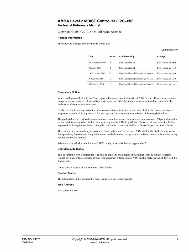
Change history
Date Issue Confidentiality Change
30 November 2007 A Non-Confidential First release for r0p0
04 April 2008 B Non-Confidential First release for r1p0
19 December 2008 C Non-Confidential Unrestricted Access First release for r2p0
01 October 2009 D Non-Confidential Unrestricted Access First release for r3p0
03 February 2010 E Non-Confidential Unrestricted Access First release for r3p1
ARM DDI 0402E Copyright © 2007-2010 ARM. All rights reserved. iiID030610 Non-Confidential
ARM DDI 0402E Copyright © 2007-2010 ARM. All rights reserved. iiiID030610 Non-Confidential
ContentsAMBA Level 2 MBIST Controller (L2C-310) Technical Reference Manual
PrefaceAbout this book ......................................................................................................... viiiFeedback .................................................................................................................... xi
Chapter 1 Introduction1.1 About the MBIST controller ...................................................................................... 1-21.2 MBIST controller interface ....................................................................................... 1-31.3 RTL configuration .................................................................................................... 1-61.4 Product revisions ..................................................................................................... 1-7
Chapter 2 Functional Description2.1 Functional overview ................................................................................................. 2-22.2 Functional operation .............................................................................................. 2-11
Chapter 3 MBIST Instruction Register3.1 About the MBIST Instruction Register ..................................................................... 3-23.2 Field descriptions ..................................................................................................... 3-3
Appendix A Signal DescriptionsA.1 MBIST controller interface signals ........................................................................... A-2A.2 Miscellaneous signals .............................................................................................. A-4
Appendix B Revisions
Glossary

List of TablesAMBA Level 2 MBIST Controller (L2C-310) Technical Reference Manual
Change history ................................................................................................................................ iiTable 1-1 Cache controller MBIST interface signals ................................................................................... 1-4Table 2-1 Cache controller compiled RAM latency ..................................................................................... 2-4Table 2-2 MBISTADDR and MBISTDIN mapping for data RAM, 8-way ..................................................... 2-5Table 2-3 MBISTADDR and MBISTDIN mapping for data RAM, 16-way ................................................... 2-5Table 2-4 Writes for data RAM testing ........................................................................................................ 2-6Table 2-5 MBISTADDR and MBISTDIN mapping for tag RAM, 8-way ....................................................... 2-6Table 2-6 MBISTADDR and MBISTDIN mapping for tag RAM, 16-way ..................................................... 2-7Table 2-7 MBISTTX signals ........................................................................................................................ 2-8Table 2-8 MBISTRX signals ........................................................................................................................ 2-9Table 2-9 MBIST controller top level I/O ..................................................................................................... 2-9Table 2-10 Data log format ......................................................................................................................... 2-13Table 3-1 Pattern field encoding ................................................................................................................. 3-3Table 3-2 Go/No-Go test pattern ................................................................................................................. 3-5Table 3-3 Control field encoding ................................................................................................................. 3-5Table 3-4 Read latency field encoding ........................................................................................................ 3-6Table 3-5 Write latency field encoding ........................................................................................................ 3-6Table 3-6 Y-address field encoding .......................................................................................................... 3-10Table 3-7 X-address field encoding .......................................................................................................... 3-10Table 3-8 Required sums of X-address and Y-address fields for data RAM ............................................ 3-11Table 3-9 Required sums of X-address and Y-address fields for tag RAM .............................................. 3-11Table 3-10 Required sums of X-address and Y-address fields for data parity RAM ................................... 3-11Table 3-11 Enables field encoding .............................................................................................................. 3-12Table 3-12 Column width field encoding ..................................................................................................... 3-13Table 3-13 Cache size field encoding ......................................................................................................... 3-13Table 3-14 Way size field encoding ............................................................................................................ 3-14Table A-1 MBIST controller interface signals .............................................................................................. A-2
ARM DDI 0402E Copyright © 2007-2010 ARM. All rights reserved. ivID030610 Non-Confidential
List of Tables
Table A-2 Miscellaneous signals ................................................................................................................. A-4Table B-1 Differences between issue C and issue D .................................................................................. B-1Table B-2 Differences between issue D and issue E .................................................................................. B-1
ARM DDI 0402E Copyright © 2007-2010 ARM. All rights reserved. vID030610 Non-Confidential

ARM DDI 0402E Copyright © 2007-2010 ARM. All rights reserved. viID030610 Non-Confidential
List of FiguresAMBA Level 2 MBIST Controller (L2C-310) Technical Reference Manual
Key to timing diagram conventions ................................................................................................ ixFigure 1-1 Cache controller MBIST configuration without data banking ...................................................... 1-2Figure 1-2 MBIST controller wiring diagram ................................................................................................. 1-3Figure 1-3 Traditional method of interfacing MBIST ..................................................................................... 1-3Figure 1-4 Cache controller MBIST interface ............................................................................................... 1-4Figure 2-1 Cache controller MBIST and RAM interfaces ............................................................................. 2-3Figure 2-2 Cache controller compiled RAM latency ..................................................................................... 2-4Figure 2-3 Cache controller MBIST paths for data RAM testing .................................................................. 2-6Figure 2-4 Cache controller MBIST paths for tag RAM testing .................................................................... 2-7Figure 2-5 MBIST controller block ................................................................................................................ 2-8Figure 2-6 Loading the MBIST controller instruction .................................................................................. 2-11Figure 2-7 Starting the MBIST test ............................................................................................................. 2-11Figure 2-8 Detecting an MBIST failure ....................................................................................................... 2-12Figure 2-9 Start of data log retrieval ........................................................................................................... 2-12Figure 2-10 End of data log retrieval ............................................................................................................ 2-13Figure 2-11 Start of bitmap data log retrieval ............................................................................................... 2-13Figure 2-12 End of bitmap data log retrieval ................................................................................................ 2-14Figure 3-1 MBIST Instruction Register ......................................................................................................... 3-2Figure 3-2 Example data RAM topology ...................................................................................................... 3-8Figure 3-3 MBIST address scrambling for normal mode .............................................................................. 3-9Figure 3-4 MBIST address scrambling for banked mode data and data parity RAM ................................... 3-9

Preface
This preface introduces the AMBA Level 2 MBIST Controller (L2C-310) Technical Reference Manual. It contains the following sections:• About this book on page viii• Feedback on page xi.
ARM DDI 0402E Copyright © 2007-2010 ARM. All rights reserved. viiID030610 Non-Confidential

Preface
About this bookThis book is for Technical Reference Manual (TRM) for the AMBA Level 2 MBIST Controller (L2C-310). In this manual the generic term MBIST controller means the AMBA Level 2 MBIST Controller, and cache controller means the AMBA Level 2 Cache Controller.
Product revision status
The rnpn identifier indicates the revision status of the product described in this book, where:rn Identifies the major revision of the product.pn Identifies the minor revision or modification status of the product.
Intended audience
This book is written for hardware engineers who are familiar with ARM technology and want to use the MBIST controller to test the RAM blocks used by the cache controller. The AXI protocol is not specified but some familiarity with AXI is assumed.
Using this book
This book is organized into the following chapters:
Chapter 1 Introduction Read this for an introduction to MBIST technology.
Chapter 2 Functional Description Read this for a description of the cache controller interface to the MBIST controller and MBIST testing of the data RAM and tag RAMs. Also read this chapter for a description of the timing sequences for loading MBIST instructions, starting the MBIST test, detecting failures, and retrieving the data log.
Chapter 3 MBIST Instruction Register Read this for a description on how to use the MBIST Instruction Register to configure the mode of operation of the MBIST engine.
Appendix A Signal Descriptions Read this for a description of the MBIST controller input and output signals.
Appendix B Revisions Read this for a description of the technical changes between released issues of this book.
Glossary Read this for definitions of terms used in this book.
Conventions
Conventions that this book can use are described in:• Typographical on page ix• Timing diagrams on page ix• Signals on page x.
ARM DDI 0402E Copyright © 2007-2010 ARM. All rights reserved. viiiID030610 Non-Confidential
Preface
Typographical
The typographical conventions are:
italic Highlights important notes, introduces special terminology, denotes internal cross-references, and citations.
bold Highlights interface elements, such as menu names. Denotes signal names. Also used for terms in descriptive lists, where appropriate.
monospace Denotes text that you can enter at the keyboard, such as commands, file and program names, and source code.
monospace Denotes a permitted abbreviation for a command or option. You can enter the underlined text instead of the full command or option name.
monospace italic Denotes arguments to monospace text where the argument is to be replaced by a specific value.
monospace bold Denotes language keywords when used outside example code.
< and > Enclose replaceable terms for assembler syntax where they appear in code or code fragments. For example:MRC p15, 0 <Rd>, <CRn>, <CRm>, <Opcode_2>
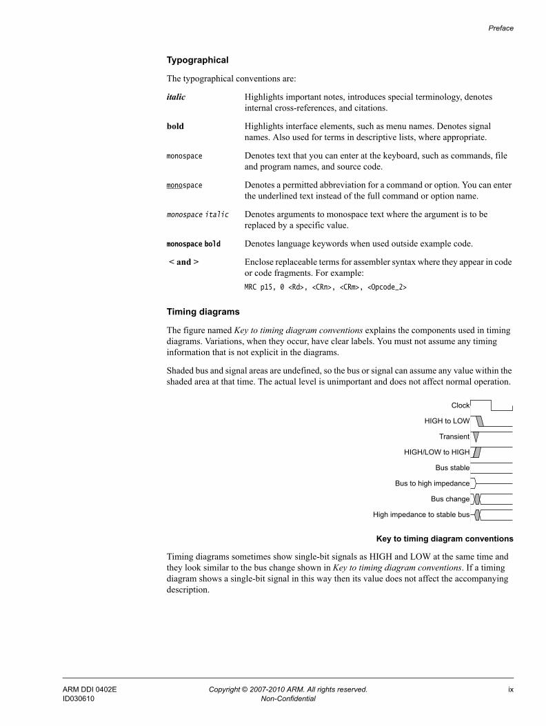
Timing diagrams
The figure named Key to timing diagram conventions explains the components used in timing diagrams. Variations, when they occur, have clear labels. You must not assume any timing information that is not explicit in the diagrams.
Shaded bus and signal areas are undefined, so the bus or signal can assume any value within the shaded area at that time. The actual level is unimportant and does not affect normal operation.
Key to timing diagram conventions
Timing diagrams sometimes show single-bit signals as HIGH and LOW at the same time and they look similar to the bus change shown in Key to timing diagram conventions. If a timing diagram shows a single-bit signal in this way then its value does not affect the accompanying description.
Clock
HIGH to LOW
Transient
HIGH/LOW to HIGH
Bus stable
Bus to high impedance
Bus change
High impedance to stable bus
ARM DDI 0402E Copyright © 2007-2010 ARM. All rights reserved. ixID030610 Non-Confidential

Preface
Signals
The signal conventions are:
Signal level The level of an asserted signal depends on whether the signal is active-HIGH or active-LOW. Asserted means:• HIGH for active-HIGH signals• LOW for active-LOW signals.
Lower-case n At the start or end of a signal name denotes an active-LOW signal.
Additional reading
This section lists publications by ARM and by third parties.
See Infocenter, http://infocenter.arm.com, for access to ARM documentation.
ARM publications
This book contains information that is specific to this product. See the following documents for other relevant information:• AMBA AXI Protocol Specification (ARM IHI 0022)• ARM Architecture Reference Manual (ARM DDI 0406)• AMBA Level 2 Cache Controller (L2C-310) Technical Reference Manual (ARM DDI
0246)• AMBA Level 2 Cache Controller (L2C-310) Implementation Guide (ARM DII 0045).
ARM DDI 0402E Copyright © 2007-2010 ARM. All rights reserved. xID030610 Non-Confidential
Preface
FeedbackARM welcomes feedback on this product and its documentation.
Feedback on this product
If you have any comments or suggestions about this product, contact your supplier and give:
• The product name.
• The product revision or version.
• An explanation with as much information as you can provide. Include symptoms and diagnostic procedures if appropriate.
Feedback on content
If you have comments on content then send an e-mail to [email protected]. Give:• the title• the number, ARM DDI 0402E• the page numbers to which your comments apply• a concise explanation of your comments.
ARM also welcomes general suggestions for additions and improvements.
ARM DDI 0402E Copyright © 2007-2010 ARM. All rights reserved. xiID030610 Non-Confidential
Chapter 1 Introduction
This chapter introduces the MBIST controller. It contains the following sections:• About the MBIST controller on page 1-2• MBIST controller interface on page 1-3• Product revisions on page 1-7.
ARM DDI 0402E Copyright © 2007-2010 ARM. All rights reserved. 1-1ID030610 Non-Confidential
Introduction
1.1 About the MBIST controllerMBIST is the industry-standard method of testing embedded memories. MBIST works by performing sequences of reads and writes to the memory according to a test algorithm. Many industry-standard test algorithms exist.
An MBIST controller generates the correct sequence of reads and writes to all locations of the RAM to ensure that the cells are operating correctly. In doing this, some additional test coverage is achieved in the address and data paths that the MBIST uses. You must only use the MBIST controller with the cache controller to perform memory testing of the Level 2 (L2) cache RAM.
Note The example integration files provided with the MBIST controller only support a 16-way cache design.
MBIST mode takes priority over all other modes, for example scan testing, in that the L2 RAMs are only accessible to the MBIST controller when MBIST mode is activated with the MTESTON pin. You must keep the MTESTON signal LOW during functional mode, and the AXI interfaces LOW during MBIST mode.
The MBIST controller controls the MBIST testing of the L2 RAMs through the MBIST port of the cache controller. Figure 1-1 shows the cache controller MBIST configuration.
When MTESTON is HIGH, the MBIST block, the cache controller, and the RAMs must be clocked at the same frequency.
Figure 1-1 Cache controller MBIST configuration without data banking
Tag RAMs (16)
Cachecontroller
MBIST block
Dispatch unit
MBIST controller
Data parity RAM (1)
Data RAM (1)
ARM DDI 0402E Copyright © 2007-2010 ARM. All rights reserved. 1-2ID030610 Non-Confidential

Introduction
1.2 MBIST controller interfaceFigure 1-2 shows the MBIST controller interface to the Automated Test Equipment (ATE) and to the MBIST interface of the cache controller.
Figure 1-2 MBIST controller wiring diagram
Figure 1-3 shows the traditional method of accessing a cache RAM for MBIST.
Figure 1-3 Traditional method of interfacing MBIST
Because this method significantly reduces the maximum operating frequency, it is not suitable for high-performance designs. Instead, the MBIST controller uses an additional input to the existing functional multiplexors without reducing maximum operating frequency.
Figure 1-4 on page 1-4 shows the five pipeline stages used to access the cache RAM arrays.
MBISTDATAIN
MBISTRESETNMTESTON
MBISTDSHIFTMBISTRUN
MBISTSHIFT
MBISTRESULT[2:0]
nRESET
CLK CLKMBISTDOUT[63:0]MBISTDCTL[19:0]
MBISTRESETNMTESTONMBISTDSHIFTMBISTRUNMBISTSHIFTMBISTDATAINMBISTRESULT[2:0]
MBISTCE[17:0]MBISTWE[31:0]
MBISTADDR[19:0]MBISTDIN[63:0]
MBISTCE[17:0]MBISTWE[31:0]MBISTADDR[19:0]MBISTDIN[63:0]
MTESTON
MBISTDCTL[19:0]MBISTDOUT[63:0]
CLKnRESET
Automated test equipment
MBIST controller Cache controller
DataInBistDataIn
01
01
AddressBistAddress
01
CEBistCE
01
WEBistWE
BistMode
RAM DataOutBistDataOut
ARM DDI 0402E Copyright © 2007-2010 ARM. All rights reserved. 1-3ID030610 Non-Confidential
Introduction
Figure 1-4 Cache controller MBIST interface
The MBIST controller accesses memory through the MBIST interface of the cache controller. Table 1-1 lists the cache controller MBIST interface signals.
MBISTADDR[19:0]
MBISTDIN[63:0]
MBISTCE[x]
MBISTWE[31:0]
MTESTON
MBISTDCTL[19:0]
Fromdata
paths
Fromaddress
paths
Fromchip
enables
Fromwrite
enables D Q
D Q
D Q
D Q
D Q
D Q
D Q
D Q
D Q
D Q
D Q
From otherRAM blocks
MBISTDOUT[63:0]
Functionaloutput
D Q
RAMblock
Table 1-1 Cache controller MBIST interface signals
Name Type Description
nRESET Input Global active LOW reset signal.
CLK Input Active HIGH clock signal. This clock drives the cache controller logic.
MBISTDOUT[63:0] Output Data out bus from all cache RAM blocks.
MBISTDCTL[19:0] Input Delayed versions of the MBISTCE[17:0] signal and the doubleword select signal, MBISTADDR[1:0]. Selects the correct read data after it passes through the MBIST pipeline stages. MBISTDCTL[19:0] = delayed {MBISTCE[17:0], MBISTADDR[1:0]}.
MTESTON Input Select signal for cache RAM array. This signal is the select input to the multiplexors that access the cache RAM arrays for test. When asserted, MTESTON takes priority over all other select inputs to the multiplexors.
MBISTCE[17:0] Input One-hot chip enables to select cache RAM arrays for test.
ARM DDI 0402E Copyright © 2007-2010 ARM. All rights reserved. 1-4ID030610 Non-Confidential

Introduction
Note The interface of the MBIST controller communicates with both the ATE and the MBIST interface of the cache controller. See Appendix A Signal Descriptions for descriptions of the MBIST controller interface signals. See the ARM AMBA Level 2 Cache Controller (L2C-310) Technical Reference Manual for more information about the MBIST interface.
MBISTWE[31:0] Input Global write enable signal for all RAM arrays.
MBISTADDR[19:0] Input Address signal for cache RAM array. MBISTADDR[1:0] is the doubleword select value. See Y-address and X-address fields, MBIR[36:33] and MBIR[40:37] on page 3-7 for a description of the doubleword select. Not all RAM arrays use the full address width.
MBISTDIN[63:0] Input Data bus to the cache RAM arrays. Not all RAM arrays use the full data width.
Table 1-1 Cache controller MBIST interface signals (continued)
Name Type Description
ARM DDI 0402E Copyright © 2007-2010 ARM. All rights reserved. 1-5ID030610 Non-Confidential

Introduction
1.3 RTL configurationL2C-310 MBIST supports, normal RAM organization, and banked RAM organization. The default is set to normal RAM organization mode so that
• bist_pl310_DATA_BANKING is commented in filelogical/pl310/verilog_mbist/pl310MBDefs.v
• pl310_DATA_BANKING is commented in filelogical/pl310/verilog/pl310_defs.v
If you want to use the banked RAM organization both of these 'defines have to be uncommented.
The banked RAM structure splits both the Data RAM and Data parity RAM into four arrays. Two dedicated L2C-310 MBIST Yaddr bits select one of the four arrays.See Y-address and X-address fields, MBIR[36:33] and MBIR[40:37] on page 3-7 for a description of the Yaddr field.
ARM DDI 0402E Copyright © 2007-2010 ARM. All rights reserved. 1-6ID030610 Non-Confidential
Introduction
1.4 Product revisionsThis section summarizes the differences in functionality between releases of the MBIST controller:
r0p0-r1p0 The difference between these revisions is additional latency cycles in MBIR. See Read latency and write latency fields, MBIR[44:41] and MBIR[48:45] on page 3-5
r1p0-r2p0 There is no functional difference between these two revisions.
r2p0-r3p0 Added support for data banking.
ARM DDI 0402E Copyright © 2007-2010 ARM. All rights reserved. 1-7ID030610 Non-Confidential

Chapter 2 Functional Description
This chapter contains a functional overview and MBIST controller implementation. The functional operation provides timing sequences for loading instructions, starting the MBIST engine, detecting failures, and retrieving the data log. It contains the following sections:• Functional overview on page 2-2• Functional operation on page 2-11.
ARM DDI 0402E Copyright © 2007-2010 ARM. All rights reserved. 2-1ID030610 Non-Confidential

Functional Description
2.1 Functional overviewThis section describes:• MBIST controller interface• MBIST controller implementation on page 2-8.
Note You must always reset the MBIST engine before you start any array test.
2.1.1 MBIST controller interface
The MBIST controller has one MBIST port, see Appendix A Signal Descriptions. Only one RAM is accessed by the MBIST controller at any time.
The MBIST controller must be able to account for the different latencies of the RAMs. You can configure RAM latencies for the cache controller RAMs. You can configure the Tag and Data RAMs for the following latencies:• setup• read access• write access.
See also Compiled RAM latencies on page 2-3.
You can use the MBIST controller for testing the cache controller compiled RAMs. You can also choose to design your own MBIST controller. You can only access one RAM by the MBIST port at a time.
Note For the MBIST to run correctly on the cache controller:• set the signals on the cache controller interface as follows:
— set ASSOCIATIVITY to the relevant value for your design— set DATAWAIT, DATAERR, TAGWAIT, and TAGERR to 0— set the AXI ports to 0.
• set the signals on the CPU as follows:— set all AXI valid bits to 0— set CLK active— disable all external request signals, for example Debug request— set the following AXI clock enables to 0, INCLKENS0, OUTCLKENS0,
INCLKENS1, OUTCLKENS1, INCLKENM0, OUTCLKENM0, INCLKENM1, and OUTCLKENM1.
Figure 2-1 on page 2-3 shows the interfaces between the MBIST controller and the RAMs that MBIST tests.
ARM DDI 0402E Copyright © 2007-2010 ARM. All rights reserved. 2-2ID030610 Non-Confidential

Functional Description
Figure 2-1 Cache controller MBIST and RAM interfaces
This section describes RAM latencies and the two MBIST RAM tests:• Compiled RAM latencies• MBIST testing of cache controller data RAM on page 2-4• MBIST testing of cache controller tag RAMs on page 2-6.
Compiled RAM latencies
The cache controller resets assuming the slowest compiled RAMs are being used. This means sixteen cache controller clock cycles are used for each access. In terms of reads, this means that the read data is sampled eight clock edges after the edge on which the read request is sampled by the RAM. Using this nomenclature, the shortest latency is one. During functional mode, the latencies for each RAM are programmed in the cache controller Auxiliary Control Register.
For MBIST, you must know the latencies of the RAMs being tested. The MBIST controller defaults to one cycle of latency, but must reprogram this during the instruction load before MBIST testing can begin. The latency of the current RAM being tested is passed to the MBIST controller in the MBIST instruction.
MBIST controller
Cache controller
Data parity RAM (1) (option)
Data RAM (1)
Tag RAMs (16)
MBISTADDR[19:0]MBISTCE[17:0]
MBISTDCTL[19:0]MBISTDIN[63:0]
MBISTDOUT[63:0]
DATAPRD[31:0]DATAPWD[31:0]DATAADDR[17:0]
DATAEN[31:0]
DATAnRWDATACS
DATARD[255:0]DATAWD[255:0]
DATAADDR[17:0]
DATAEN[31:0]
DATAnRWDATACS
TAGRDx[20:0]TAGPRD[15:0]
TAGADDR[13:0]TAGWD[20:0]TAGCS[15:0]
TAGnRWTAGEN[20:0]
TAGPWD
MTESTON
TAGPEN
MBISTWE[31:0]
TAGLWDTAGLEN
TAGLRD[15:0]
ARM DDI 0402E Copyright © 2007-2010 ARM. All rights reserved. 2-3ID030610 Non-Confidential

Functional Description
Table 2-1 shows the cache controller compiled RAM latency.
Figure 2-2 shows the cache controller compiled RAM latency.
Figure 2-2 Cache controller compiled RAM latency
MBIST testing of cache controller data RAM
The cache controller data RAM is 256 bits wide, and the size of the MBISTDIN and MBISTDOUT buses on the cache controller MBIST interface is 64 bits, so four reads and four writes are required for each index of the data RAM. The cache controller handles this by using the MBISTADDR[1:0] signal as a doubleword select for each index of the data RAM for writes. For reads from a previous MBIST transaction you use the MBISTDCTL[1:0] signal. You require separate pins because the MBIST transactions are pipelined. The MBIST controller
Table 2-1 Cache controller compiled RAM latency
Latency bits [3:0] Cycles of latency
4’b0000 1 cycle of latency. No additional latency. This is the default.
4’b0001 2 cycles of latency.
4’b0010 3 cycles of latency.
4’b0011 4 cycles of latency.
4’b0100 5 cycles of latency.
4’b0101 6 cycles of latency.
4’b0110 7 cycles of latency.
4’b0111 8 cycles of latency.
4’b1000 9 cycles of latency.
4’b1001 10 cycles of latency.
4’b1010 11 cycles of latency.
4’b1011 12 cycles of latency.
4’b1100 13 cycles of latency.
4’b1101 14 cycles of latency.
4’b1110 15 cycles of latency.
4’b1111 16 cycles of latency.
data
data
data
CLK
Chip select
Cache controller compiled RAM latency = 0000
Cache controller compiled RAM latency = 0001
Cache controller compiled RAM latency = 0010
ARM DDI 0402E Copyright © 2007-2010 ARM. All rights reserved. 2-4ID030610 Non-Confidential

Functional Description
takes into account the data RAM latency and issues the correct control signals. Table 2-2 shows the address range of the MBISTADDR bus used to test the data RAM, based on the L2 cache size and configured to be 8-way.
For a 16-way cache, you can remove one bit from the lower address range and add it to the upper address range as compared to an 8-way cache of the same size. Table 2-3 shows the address range of the MBISTADDR bus used to test the data RAM, based on the L2 cache size and configured to be 16-way.
The cache controller has a 256-bit wide Line Read Buffer (LRB) in each slave. One of these holds data for MBIST testing. The cache controller always adds two register delays to the MBIST data read path for the data RAM.
When using the MBIST controller you must account for the data RAM latency in the pipeline. The latency can be from one to eight clock cycles. See Compiled RAM latencies on page 2-3. The signal MBISTCE[0] is for the chip enable to the data RAM. The signal MBISTDCTL[2:0] is for reads from previous MBIST transactions.
Figure 2-3 on page 2-6 shows the cache controller MBIST paths for data RAM testing.
Table 2-2 MBISTADDR and MBISTDIN mapping for data RAM, 8-way
L2 cache size
Number of data RAM indexes
MBISTADDR to data RAM mapping MBISTDIN to data RAM mapping
128KB 4,096 DATAADDR[11:0]=MBISTADDR[18:16,10:2] DATAWD[63:0]=MBISTDIN[63:0]
256KB 8,192 DATAADDR[12:0]=MBISTADDR[18:16,11:2] DATAWD[63:0]=MBISTDIN[63:0]
512KB 16,384 DATAADDR[13:0]=MBISTADDR[18:16,12:2] DATAWD[63:0]=MBISTDIN[63:0]
1MB 32,768 DATAADDR[14:0]=MBISTADDR[18:16,13:2] DATAWD[63:0]=MBISTDIN[63:0]
2MB 65,536 DATAADDR[15:0]=MBISTADDR[18:16,14:2] DATAWD[63:0]=MBISTDIN[63:0]
4MB 131,072 DATAADDR[16:0]=MBISTADDR[18:2] DATAWD[63:0]=MBISTDIN[63:0]
Table 2-3 MBISTADDR and MBISTDIN mapping for data RAM, 16-way
L2 cache size
Number of data RAM indexes
MBISTADDR to data RAM mapping MBISTDIN to data RAM mapping
256KB 8,192 DATAADDR[12:0]=MBISTADDR[19:16,10:2] DATAWD[63:0]=MBISTDIN[63:0]
512KB 16,384 DATAADDR[13:0]=MBISTADDR[19:16,11:2] DATAWD[63:0]=MBISTDIN[63:0]
1MB 32,768 DATAADDR[14:0]=MBISTADDR[19:16,12:2] DATAWD[63:0]=MBISTDIN[63:0]
2MB 65,536 DATAADDR[15:0]=MBISTADDR[19:16,13:2] DATAWD[63:0]=MBISTDIN[63:0]
4MB 131,072 DATAADDR[16:0]=MBISTADDR[19:16,14:2] DATAWD[63:0]=MBISTDIN[63:0]
8MB 262,144 DATAADDR[17:0]=MBISTADDR[19:2] DATAWD[63:0]=MBISTDIN[63:0]
ARM DDI 0402E Copyright © 2007-2010 ARM. All rights reserved. 2-5ID030610 Non-Confidential
Functional Description
Figure 2-3 Cache controller MBIST paths for data RAM testing
Table 2-4 shows the write sequences for data RAM testing.
MBIST testing of cache controller tag RAMs
There is one tag RAM for each way of the L2 cache. The maximum number of tag RAMs the MBIST controller has to test is 16. Only one tag RAM is tested at a time. Table 2-5 shows the address range of the MBISTADDR bus used to test a tag RAM, based on the L2 cache size and configured to be 8-way. The parity for each tag RAM present is tested along with the rest of the tag and is mapped to MBISTDIN[22]. Lockdown by line is tested with the rest of the tag and is mapped to MBISTDIN[21].
For all cases:• lockdown by line TAGLWD=MBISTDIN[21]
MbistaddrD1[17:0]MbistceD1[0]
MbistdinD1[63:0]MbistweD1
DATAADDR[16:0]DATACS
DATAEN[31:0]DATAWD[255:0]
DATARD[255:0]
MbistdctlD1[2:0]MtestonD1 Data RAM
LRB0MBISTDOUT[63:0]
MBISTADDR[19:0]MBISTCE[17:0]=h001
MBISTDIN[63:0]MBISTDCTL[19:0]
MBISTWE[31:0]MTESTON
MtestonD1
64256
Table 2-4 Writes for data RAM testing
MBISTADDR[1:0] DATAEN[31:0] DATAWD used
b00 0x000F [63:0]
b01 0x00F0 [127:64]
b10 0x0F00 [191:128]
b11 0xF000 [255:192]
Table 2-5 MBISTADDR and MBISTDIN mapping for tag RAM, 8-way
L2 cache size
Way size
Number of tag RAM indexes
MBISTADDR to tag RAM mapping MBISTDIN to tag RAM mapping
128KB 16KB 512 TAGADDR[8:0]=MBISTADDR[10:2] TAGWD[20:0]=MBISTDIN[20:0]
256KB 32KB 1,024 TAGADDR[9:0]=MBISTADDR[11:2] TAGWD[20:1]=MBISTDIN[20:1]
512KB 64KB 2,048 TAGADDR[10:0]=MBISTADDR[12:2] TAGWD[20:2]=MBISTDIN[20:2]
1MB 128KB 4,096 TAGADDR[11:0]=MBISTADDR[13:2] TAGWD[20:3]=MBISTDIN[20:3]
2MB 256KB 8,192 TAGADDR[12:0]=MBISTADDR[14:2] TAGWD[20:4]=MBISTDIN[20:4]
4MB 512KB 16,384 TAGADDR[13:0]=MBISTADDR[15:2] TAGWD[20:5]=MBISTDIN[20:5]
ARM DDI 0402E Copyright © 2007-2010 ARM. All rights reserved. 2-6ID030610 Non-Confidential

Functional Description
• parity TAGPWD=MBISTDIN[22].
Table 2-6 shows the address range of the MBISTADDR bus used to test the tag RAM, based on the L2 cache size and configured to be 16-way.
The data from the tag RAMs is always registered by the cache controller. There is a register on the MBIST port of the cache controller. Consequently, to the MBIST controller, the cache controller always adds two register delays to the MBIST data read path for the tag RAMs.
When using the MBIST controller you must account for the Tag RAM latency in the pipeline. The signal MBISTCE[16:1] is for chip enables to the tag RAMs. The signal MBISTDCTL[18:3] is for reads from previous MBIST transactions. The latency of the tag RAMs can be from one to eight clock cycles. See Compiled RAM latencies on page 2-3.
Figure 2-4 shows the cache controller MBIST paths for tag RAM testing.
Figure 2-4 Cache controller MBIST paths for tag RAM testing
Note • MBISTCE[16:1] corresponds to TAGCS[15:0]• MDBISTDCL[18:3] corresponds to TAG[15:0]• Only bits [22:0] of MBISTDIN and MBISTDOUT are used.
Table 2-6 MBISTADDR and MBISTDIN mapping for tag RAM, 16-way
L2 cache size
Way size
Number of tag RAM indexes
MBISTADDR to tag RAM mapping MBISTDIN to tag RAM mapping
256KB 16KB 512 TAGADDR[8:0]=MBISTADDR[10:2] TAGWD[20:0]=MBISTDIN[20:0]
512KB 32KB 1,024 TAGADDR[9:0]=MBISTADDR[11:2] TAGWD[20:1]=MBISTDIN[20:1]
1MB 64KB 2,048 TAGADDR[10:0]=MBISTADDR[12:2] TAGWD[20:2]=MBISTDIN[20:2]
2MB 128KB 4,096 TAGADDR[11:0]=MBISTADDR[13:2] TAGWD[20:3]=MBISTDIN[20:3]
4MB 256KB 8,192 TAGADDR[12:0]=MBISTADDR[14:2] TAGWD[20:4]=MBISTDIN[20:4]
8MB 512KB 16,384 TAGADDR[13:0]=MBISTADDR[15:2] TAGWD[20:5]=MBISTDIN[20:5]
TAGRD0-15[20:0]TAGLRD[15:0]TAGPRD[15:0]
MbistaddrD1[14:2]MbistceD1[16:1]
MbistdinD1[22:0]MbistweD1
TAGADDR[12:0]TAGCS[15:0]
TAGENTAGWD[20:0]
TAGPWD TAGPEN TAGLWD TAGLEN
MbistdctlD1[10:3]MtestonD1
Up to sixteen tag RAMS
MBISTADDR[19:0]MBISTCE[17:0]
MBISTDIN[63:0]MBISTDCTL[19:0]
MBISTWE[31:0]MTESTON
MtestonD1
MBISTDOUT[63:0]
2364
ARM DDI 0402E Copyright © 2007-2010 ARM. All rights reserved. 2-7ID030610 Non-Confidential

Functional Description
2.1.2 MBIST controller implementation
The MBIST controller block shown in Figure 2-5 consists of:• MBIST controller• dispatch unit.
Figure 2-5 MBIST controller block
This section describes:• MBIST controller and dispatch unit interface• MBIST controller block top level I/O on page 2-9.
MBIST controller and dispatch unit interface
The MBIST controller and the dispatch unit communicate using the following signals:
MBISTTX[11:0] This signal is an output of the MBIST controller that goes to the dispatch unit. Table 2-7 shows the signals.
When the instruction shift is enabled, data shifts between the two parts of the BIST engine are on bit 3. In run test mode, this bit is used as invert data information. The MBISTTX[11:0] interface is ARM-specific and intended for use only with the MBIST controller.
MBIST controller Dispatch unitMBISTTX[11:0]
MBISTRX[2:0]
MBIST controller block
Table 2-7 MBISTTX signals
MBISTTX bit Description
0 Reset address
1 Increment address
2 Access sacrificial row, used during bang patterns
3 Invert data/instruction data in
4 Checkerboard data
5 Write data
6 Read data
7 Yfast/nXfast
8 Direction
9 Enable bitmap mode
10 Increment go/nogo dataword selection
11 Latency stall control
ARM DDI 0402E Copyright © 2007-2010 ARM. All rights reserved. 2-8ID030610 Non-Confidential

Functional Description
MBISTRX[2:0] This signal is an output of the dispatch unit that goes to the MBIST controller. The behavior of MBISTRX[2:0] is ARM-specific and is intended for use only with the MBIST controller. The address expire signal is set when both the row and column address counters expire. Table 2-8 shows the signals.
MBIST controller block top level I/O
The top level I/O of the MBIST controller consists of the cache controller interface. See Appendix A Signal Descriptions, and the inputs and outputs that Table 2-9 shows.
Note nRESET of the cache controller must be HIGH in MBIST test mode.
The following signals have additional information:
SE Preservation of array state is required when performing multiload Automatic Test Pattern Generator (ATPG) runs or when performing Integrated Circuit Quiescent Current (IDDQ) testing. After performing MBIST tests to initialize the arrays to a required background, the ATPG test procedures must assert SE during all test setup cycles in addition to load/unload. Any clocking during IDDQ capture cycles must have array chip select signals constrained.
Table 2-8 MBISTRX signals
MBISTRX bit Description
0 Address/instruction data out/fail data out
1 Shadow pipeline empty
2 Nonsticky fail flag
Table 2-9 MBIST controller top level I/O
Signal Direction Function Value, MBIST mode Value, function mode
MBISTDATAIN Input Serial data in Toggle 0
MBISTDSHIFT Input Data log shift Toggle 0
MBISTRESETN Input MBIST reset Toggle 0a
MBISTRESULT[2:0] Output Output status bus Strobe -
MBISTRUN Input Run MBIST test Toggle 0
MBISTSHIFT Input Instruction shift Toggle 0
MTESTON Input MBIST path enable Toggle 0a
SE Input ATPG signal 0 0
a. Must be LOW in functional mode.
ARM DDI 0402E Copyright © 2007-2010 ARM. All rights reserved. 2-9ID030610 Non-Confidential

Functional Description
MBISTRESULT[2:0] During tests, the MBISTRESULT[1] signal indicates failures. You can operate using two modes, by configuring bit 5 of the engine control section of the instruction register. If bit 5 is set, the MBISTRESULT[1] signal is asserted for a single cycle for each failed compare. If bit 5 is not set, the MBISTRESULT[1] signal is sticky, and is asserted from the first failure until the end of the test.At the completion of the test, the MBISTRESULT[2] signal goes HIGH. The MBISTRESULT[0] signal indicates that an address expire has occurred and enables you to measure sequential progress through the test algorithms.
ARM DDI 0402E Copyright © 2007-2010 ARM. All rights reserved. 2-10ID030610 Non-Confidential

Functional Description
2.2 Functional operationThe functional operation is described in:• Timing• Bitmap mode on page 2-13.
2.2.1 Timing
A 60-bit instruction, loaded serially at the start of each test, controls the operation of the MBIST controller. Chapter 3 MBIST Instruction Register describes how to write the instruction.
The timing diagrams in this section show the clock running at two different speeds:• the slower clock relates to the clock driven by your ATE• the faster clock relates to the clock driven by an on-chip Phase Locked Loop (PLL).
If you do not have an on-chip PLL, both clocks relate to the clock driven by your ATE.
Timing diagrams in the following sections show the procedures for operating the MBIST controller: • Instruction load• Starting MBIST• Failure detection on page 2-12• Data log retrieval on page 2-12.
Instruction load
To load an MBIST instruction, drive MBISTSHIFT HIGH. At the next rising clock edge, the 61-bit shift sequence begins as shown in Figure 2-6. To enable data input from the ATE, the PLL is in bypass mode, and the clock is not running at test frequency.
Figure 2-6 Loading the MBIST controller instruction
Starting MBIST
Reset the MBIST engine. After loading the MBIST instruction, drive MBISTSHIFT LOW and disable CLK. With CLK disabled, drive MBISTRUN HIGH and, after an MBISTRUN setup time, start the PLL at the test frequency as shown in Figure 2-7.
Figure 2-7 Starting the MBIST test
i[60]i[59]i[1]i[0]
CLK
MBISTRUN
MBISTSHIFT
MBISTDATAIN
CLK
MBISTRUN
MBISTSHIFT
ARM DDI 0402E Copyright © 2007-2010 ARM. All rights reserved. 2-11ID030610 Non-Confidential
Functional Description
Failure detection
The MBISTRESULT[1] flag goes HIGH two CLK cycles after the controller detects a failure, as Figure 2-8 shows. It stays HIGH if sticky fail is enabled. If stop on fail is enabled, the MBISTRESULT[2] flag goes HIGH two cycles later.
Figure 2-8 Detecting an MBIST failure
Note To ensure that the ATE can observe a failure at test speed, specify a sticky fail in the MBIST instruction. See Control field, MBIR[54:49] on page 3-5.
Data log retrieval
During a test, the MBIST controller automatically logs the first detected failure. If required, you can retrieve the data log at the end of the test to generate failure statistics. Figure 2-9 and Figure 2-10 on page 2-13 show the method of retrieving a data log.
Note MBISTRESULT[0] is the serial data output for instructions and the data log.
After the MBISTRESULT[2] flag goes HIGH, stop the test by putting the PLL in bypass mode and driving MBISTRUN LOW as Figure 2-9 shows. To begin shifting out the data log on MBISTRESULT[0], drive MBISTDSHIFT HIGH. The MBISTRESULT[2] flag goes LOW two cycles after MBISTRUN goes LOW. Data begins shifting out on MBISTRESULT[0] two cycles after MBISTDSHIFT goes HIGH.
Figure 2-9 Start of data log retrieval
When the last data log bit shifts out, drive MBISTDSHIFT LOW as Figure 2-10 on page 2-13 shows.
With stop-on-fail enabled andonly one cycle of latency
With sticky fail enabled
CLK
MBISTRESULT[1] (fail flag)
MBISTRESULT[2] (complete flag)
CLK
MBISTRESULT[2](complete flag)
MBISTDSHIFT
MBISTRESULT[0](data log shift out)
MBISTRUN
D[0]
ARM DDI 0402E Copyright © 2007-2010 ARM. All rights reserved. 2-12ID030610 Non-Confidential

Functional Description
Figure 2-10 End of data log retrieval
Table 2-10 shows the format of the data log.
The address contained in the data log refers to the full address of the failing location as it appears on the MBISTADDR[19:0] port of the MBIST interface of the cache controller. It always includes the doubleword select value in the least significant two bits. See Y-address and X-address fields, MBIR[36:33] and MBIR[40:37] on page 3-7 for more information on the doubleword select value. Contact ARM if you require more information.
2.2.2 Bitmap mode
In bitmap mode, you can identify all failing locations in a RAM. Each time a failure occurs, the controller stops executing the current test and waits for you to begin shifting out the data log as Figure 2-11 shows.
Figure 2-11 Start of bitmap data log retrieval
After you finish shifting and drive MBISTDSHIFT LOW, the controller then resumes testing where it stopped as Figure 2-12 on page 2-14 shows. This process continues until the test algorithm completes. A fault can cause a failure to occur several times during a given test algorithm. The fault might be logged multiple times depending on the number of reads performed by the algorithm and the exact nature of the fault.
MBISTRESULT[2]
MBISTDSHIFT
MBISTRESULT[0]
MBISTRUN
D[85]D[84]D[83]
CLK
Table 2-10 Data log format
Bits Description
[87:68] Address of the failing location.
[67:4] Failing data bits. These bits are set for faulty bits and cleared for passing bits.
[3:0] The data seed used in the test. See Data seed field, MBIR[32:29] on page 3-12.
CLK
MBISTRESULT[1](fail flag)
MBISTDSHIFT
MBISTRESULT[0](data log shift out)
MBISTRUN
D[0]
ARM DDI 0402E Copyright © 2007-2010 ARM. All rights reserved. 2-13ID030610 Non-Confidential

Functional Description
Figure 2-12 End of bitmap data log retrieval
Loading a new instruction resets bitmap mode.
D[83] D[84] D[85]
CLK
MBISTRESULT[1]
MBISTDSHIFT
MBISTRESULT[0]
MBISTRUN
ARM DDI 0402E Copyright © 2007-2010 ARM. All rights reserved. 2-14ID030610 Non-Confidential
Chapter 3 MBIST Instruction Register
This chapter describes how to use the MBIST Instruction Register (MBIR) to configure the mode of operation of the MBIST controller. It contains the following sections:• About the MBIST Instruction Register on page 3-2• Field descriptions on page 3-3.
ARM DDI 0402E Copyright © 2007-2010 ARM. All rights reserved. 3-1ID030610 Non-Confidential

MBIST Instruction Register
3.1 About the MBIST Instruction RegisterFigure 3-1 shows the bit fields of the MBIR.
Figure 3-1 MBIST Instruction Register
The MBIR fields set up the behavior of the MBIST engine:
Pattern Specifies the test algorithm.
Control Specifies MBIST mode of operation and sticky or nonsticky fail flag.
Write latency Specifies the number of cycles to enable a RAM write.
Read latency Specifies the number of cycles to enable a RAM read.
X addr Specifies the number of bits in the X-address counter.
Y addr Specifies the number of bits in the Y-address counter.
Data seed Specifies the four-bit data background.
Enables Specifies the RAM under test.
Column width Specifies 4, 8, 16, or 32 columns per block of RAM.
Cache size Specifies a cache size of 128KB, 256KB, 512KB, 1MB, 2MB, 4MB, or 8MB.
Way size Specifies a way size of 16KB, 32KB, 64KB, 128KB, 256KB, or 512KB.
Parity support Specifies if parity is supported.
Lockdown by line support Specifies if lockdown by line is supported.
Way configuration Specifies an 8-way or 16-way configuration.
Field descriptions on page 3-3 describes the MBIR fields in more detail.
60 55 54 4948 4544 41 40 3736 33 32 8 62928 91011
Pattern Control Read latency X Addr Y Addr Data
seed Enables
Cache sizeColumn width
5 12 03
Way sizeParity support
Lock by line supportWay configuration
Write latency
ARM DDI 0402E Copyright © 2007-2010 ARM. All rights reserved. 3-2ID030610 Non-Confidential

MBIST Instruction Register
3.2 Field descriptionsThe following sections describe the MBIR fields:• Pattern field, MBIR[60:55]• Control field, MBIR[54:49] on page 3-5• Read latency and write latency fields, MBIR[44:41] and MBIR[48:45] on page 3-5• Y-address and X-address fields, MBIR[36:33] and MBIR[40:37] on page 3-7• Data seed field, MBIR[32:29] on page 3-12• Enables field, MBIR[28:11] on page 3-12• Column width field, MBIR[10:9] on page 3-13• Cache size field, MBIR[8:6] on page 3-13• Way size field, MBIR[5:3] on page 3-14• Parity support field, MBIR[2] on page 3-14• Lockdown by line support field, MBIR[1] on page 3-14• Way configuration field, MBIR[0] on page 3-14.
3.2.1 Pattern field, MBIR[60:55]
The MBIST controller is supplied with industry-standard pattern algorithms and a bit-line stress algorithm. You can group algorithms together to create a specific memory test methodology for your product.
Table 3-1 describes the supported algorithms, and Pattern specification on page 3-4 describes their use. The N values in the table indicate the number of RAM accesses per address location and give an indication of the test time when using that algorithm.
Table 3-1 Pattern field encoding
Pattern MBIR[60:55] Algorithm name N Description
b000000 Write Solids 1N Write a solid pattern to memory
b000001 Read Solids 1N Read a solid pattern from memory
b000010 Write Checkerboard 1N Write a checkerboard pattern to memory
b000011 Read Checkerboard 1N Read a checkerboard pattern from memory
b000100 March C+ (x-fast) 14N March C+ algorithm, incrementing X-address first
b001011 March C+ (y-fast) 14N March C+ algorithm, incrementing Y-address first
b000101 Fail Pattern 6N Tests memory failure detection capability
b000110 Read Write March (x-fast) 6N Read write march pattern, incrementing X-address first
b000111 Read Write March (y-fast) 6N Read write march pattern incrementing Y-address first
b001000 Read Write Read March (x-fast) 8N Read write read march pattern, incrementing X-address first
b001001 Read Write Read March (y-fast) 8N Read write read march pattern, incrementing Y-address first
b001010 Bang 18N Bit-line stress pattern
b111111 Go/No-Go 30N See Table 3-2 on page 3-5
ARM DDI 0402E Copyright © 2007-2010 ARM. All rights reserved. 3-3ID030610 Non-Confidential

MBIST Instruction Register
Pattern specification
This section describes the MBIST test patterns. An x-fast pattern increments or decrements the X-address counter first. A y-fast pattern increments or decrements the Y-address counter first. Y-address and X-address fields, MBIR[36:33] and MBIR[40:37] on page 3-7 describes the X-address and Y-address counters.
The first four patterns are useful for data retention or IDDQ testing.
Write Solids This initializes the RAM with the supplied data seed.
Read Solids This reads each RAM location once expecting the supplied data seed.
Write Checkerboard This initializes the RAM with a physical checkerboard pattern created by alternating the supplied data seed and its inverse.
Read Checkerboard This reads back the physical checkerboard pattern created by alternating the supplied data seed and its inverse.
For the next set of patterns, the following notation describes the algorithm:• 0 represents the data seed• 1 represents the inverse data seed• w indicates a write operation• r indicates a read operation• incr indicates that the address is incremented• decr indicates that the address is decremented.
March C+ (x-fast or y-fast) This is the industry-standard March C+ algorithm:(w0) (r0, w1, r1) (r1, w0, r0) decr (r0, w1, r1) decr (r1, w0, r0) (r0)
Read Write March (x-fast or y-fast) (w0) (r0, w1) decr (r1, w0) (r0)
Read Write Read March (x-fast or y-fast) (w0) (r0, w1, r1) decr (r1, w0, r0) (r0)
Bang This test is always performed in x-fast. It executes multiple consecutive writes and reads effectively stressing a bit-line pair. While this pattern does detect stuck-at faults, its primary intent is to address the analog characteristics of the memory. In the following algorithm description, row 0 indicates a read or write of the data seed to the sacrificial row, this is always the first row of the column being addressed.(w0) (r0, w0, w0(row 0) × 6) (r0 × 5, w0(row 0), r0) (r0)
ARM DDI 0402E Copyright © 2007-2010 ARM. All rights reserved. 3-4ID030610 Non-Confidential

MBIST Instruction Register
Go/No-Go If you do not want to implement your own memory test strategy, use the Go/No-Go test pattern that performs the algorithms that Table 3-2 shows.
This test suite provides a comprehensive test of the arrays. The series of tests in Go/No-Go are the result of the experience in memory testing by ARM memory test engineers.
3.2.2 Control field, MBIR[54:49]
The control field specifies the MBIST function. Table 3-3 shows how the control field affects the behavior of the MBIST controller.
MBIR[54] selects a nonsticky or sticky fail flag, MBISTRESULT[1]:
• When MBIR[54] is set, the fail bit toggles in real time. It goes HIGH for failing comparisons and LOW for passing comparisons.
Note Setting MBIR[54] can cause the fail bit to toggle at the test frequency. It is not
recommended when the external pin or the ATE cannot follow the test frequency.
• When MBIR[54] is cleared, the fail bit is sticky. It remains HIGH after the first failure until a new MBIST instruction shifts in or until the data log shifts out.
3.2.3 Read latency and write latency fields, MBIR[44:41] and MBIR[48:45]
The read latency and write latency fields of the MBIR are used to specify the read and write latency of the RAM under test. Read and write latencies are the numbers of cycles that the RAM requires to complete read and write operations. For example, in a write to a RAM with a write latency of two cycles, the RAM inputs are valid for a single cycle. The next cycle is a NOP cycle
Table 3-2 Go/No-Go test pattern
Sequence Algorithm Data
1 Write Checkerboard Data seed
2 Read Checkerboard Data seed
3 Write Checkerboard Data seed
4 Read Checkerboard Data seed
5 Read Write Read March (y-fast) 0x6
6 Bang 0xF
Table 3-3 Control field encoding
ControlMBIR[54:49] Behavior Description
bx00000 Default Test runs to completion. If MBIR[54] = 0, sticky fail present after first failure.
bx00001 Stop on fail End of test on failure.
bx00011 Bitmap mode Enables logging of each failure. See Bitmap mode on page 2-13.
ARM DDI 0402E Copyright © 2007-2010 ARM. All rights reserved. 3-5ID030610 Non-Confidential

MBIST Instruction Register
with the chip enable negated. Similarly, in a read from a RAM with a read latency of three cycles, the RAM inputs are valid for a single cycle. After two NOP cycles, the read data is valid on the RAM outputs.
Note Even if the RAM under test uses the same latency for both read and write operations, you must still program both the read latency and write latency fields of the MBIR with the same value.
Table 3-4 shows the latency settings for read operations.
Table 3-5 shows the latency settings for write operations.
Table 3-4 Read latency field encoding
Read latencyMBIR[44:41]
Number of cyclesper read operation
b0000 1
b0001 2
b0010 3
b0011 4
b0100 5
b0101 6
b0110 7
b0111 8
b1000 9
b1001 10
b1010 11
b1011 12
b1100 13
b1101 14
b1110 15
b1111 16
Table 3-5 Write latency field encoding
Write latencyMBIR[48:45]
Number of cyclesper write operation
b0000 1
b0001 2
b0010 3
b0011 4
b0100 5
ARM DDI 0402E Copyright © 2007-2010 ARM. All rights reserved. 3-6ID030610 Non-Confidential

MBIST Instruction Register
3.2.4 Y-address and X-address fields, MBIR[36:33] and MBIR[40:37]
You can determine the number of address bits you must specify for a RAM from the MBIR fields:• X-address• Y-address.
This enables you to specify your address range in two dimensions, this represents the topology of the physical implementation of the RAM more accurately. These two dimensions are controlled by two separate address counters, the X-address counter and the y-address counter. One counter can be incremented or decremented only when the other counter has expired. The chosen test algorithm determines the counter that moves faster.
Normal mode
Use this procedure to determine how many bits to assign to the X-address and Y-address counters:
1. Determine the column width of the RAM array. The Y-address must have at least that many bits for the column select. If it is a Data RAM, add two bits to that number for the doubleword select.
2. Determine how many address bits the RAM requires. See Cache controller RAMs on page 3-11. Subtract the current Y-address bit number from that number. If the result is eight or fewer bits, they are all assigned to the X-address for the row select. Otherwise, eight bits are used for the X-address and any unassigned bits are added to the bits already assigned to the Y-address and used for the block select.
Figure 3-2 on page 3-8 shows an example topology for the Data RAM in a 256K level-2 cache.
b0101 6
b0110 7
b0111 8
b1000 9
b1001 10
b1010 11
b1011 12
b1100 13
b1101 14
b1110 15
b1111 16
Table 3-5 Write latency field encoding (continued)
Write latencyMBIR[48:45]
Number of cyclesper write operation
ARM DDI 0402E Copyright © 2007-2010 ARM. All rights reserved. 3-7ID030610 Non-Confidential

MBIST Instruction Register
Figure 3-2 Example data RAM topology
The cache RAM in Figure 3-2 has a column width of 16, so it uses four bits for the column address. These four bits map to the least significant bits of the Y-address counter. Because this is a data RAM, it requires two additional doubleword select bits. The doubleword select bits choose between the four 64-bit groups of RAM data before sending the data to the 64-bit MBISTDOUT[63:0] bus. These two bits always map to the Y-address counter bits between the column address and the block address.
Because this cache RAM has 256 rows per column, it uses eight bits for the row address, this uses up all eight bits of the X-address counter. This RAM also contains two blocks of 16 columns each, so it uses one bit for the block address. This maps to the most significant bit of the Y-address counter. To correctly test this RAM, the Y-address field must have a value of seven, MBIR[36:33] = b0111, and the X-address field must have a value of eight, MBIR[40:37] = b1000. Values higher or lower than these produce incorrect results.
Note If the columns have fewer than 256 rows, you must still assign address bits to the row address until all eight bits are used before assigning any to the block address. If the cache RAM has more than 256 rows per column, then the additional bits must be assigned to the block address. This does not have any detrimental effects on the test coverage of the RAM.
Figure 3-3 on page 3-9 shows how the MBIST controller builds the address output. The doubleword select bits are the least significant two bits of the address. These two bits are ignored unless the data RAM is selected. The exclusive OR of the two least significant bits of the Y-address counter is the least significant bit of the column address for physical addressing of the columns. This is followed by the row address from the X-address counter and, if required, the block address.
Column 0 Column 15
X-address(rows)
LowerY-address(columns)
255 0 255 0
Block 0
Data Out [255:0]
Block 1
UpperY-address
(blocks)
MBISTDOUT[63:0]
Doubleword select(data RAM only)
...
...
...
Column 0 Column 15255 0 255 0
...
...
...
255
0
255
0
255
0
255
0
ARM DDI 0402E Copyright © 2007-2010 ARM. All rights reserved. 3-8ID030610 Non-Confidential

MBIST Instruction Register
Figure 3-3 MBIST address scrambling for normal mode
Banked RAM organization
The X-address field for banked RAM is determined the same way as in normal RAM mode. For both data RAM and data parity RAM, the Y-address field is same as in normal RAM mode but with the addition of two bits to select the RAM bank.
Tag RAM address mapping for banked RAM is the same as non-banked RAM. See Figure 3-3.
Figure 3-4 shows the structure for banked mode data RAM and banked mode data parity RAM.The only difference from normal mode RAM is that two of the Y-address counter bits now form the Bank select.
Figure 3-4 MBIST address scrambling for banked mode data and data parity RAM
01
01
9
23
. . .. . .
. . .. . .
7 6 5 4 3 2 1 0
X-address counter Y-address counter
Blockaddress
Rowaddress
Columnaddress
Double-word selectMBISTADDR[19:0]
19
01
01
9
23
. . .. . .
. . .. . .
7 6 5 4 3 2 1 0
X-address counter Y-address counter
Blockaddress
Rowaddress
Columnaddress
Double-word select
MBISTADDR[19:0]
19
45
Bank select
ARM DDI 0402E Copyright © 2007-2010 ARM. All rights reserved. 3-9ID030610 Non-Confidential
MBIST Instruction Register
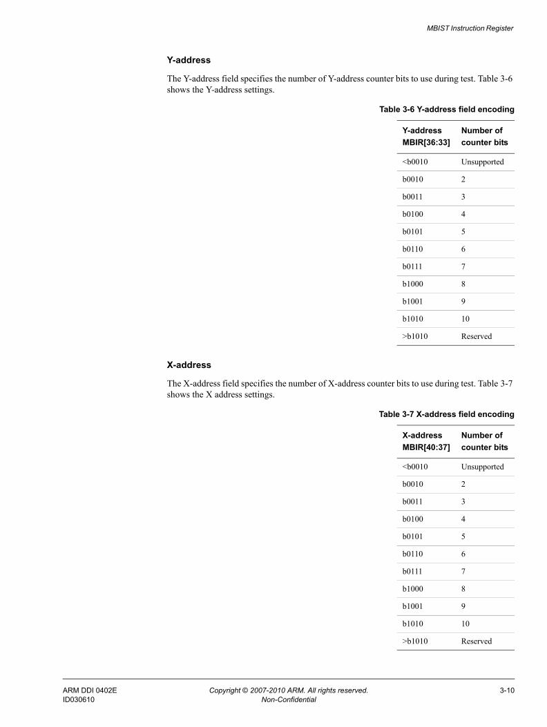
Y-address
The Y-address field specifies the number of Y-address counter bits to use during test. Table 3-6 shows the Y-address settings.
X-address
The X-address field specifies the number of X-address counter bits to use during test. Table 3-7 shows the X address settings.
Table 3-6 Y-address field encoding
Y-addressMBIR[36:33]
Number ofcounter bits
<b0010 Unsupported
b0010 2
b0011 3
b0100 4
b0101 5
b0110 6
b0111 7
b1000 8
b1001 9
b1010 10
>b1010 Reserved
Table 3-7 X-address field encoding
X-addressMBIR[40:37]
Number ofcounter bits
<b0010 Unsupported
b0010 2
b0011 3
b0100 4
b0101 5
b0110 6
b0111 7
b1000 8
b1001 9
b1010 10
>b1010 Reserved
ARM DDI 0402E Copyright © 2007-2010 ARM. All rights reserved. 3-10ID030610 Non-Confidential

MBIST Instruction Register
Cache controller RAMs
Table 3-8 shows the required sums of the X-address and Y-address fields for testing of data RAM.
Table 3-9 shows the required sums of the X-address and Y-address fields for testing of tag RAM.
Table 3-10 shows the required sums of the X-address and Y-address fields for testing of data parity RAM.
Table 3-8 Required sums of X-address and Y-address fields for data RAM
Cache size Data RAM
128KB 14
256KB 15
512KB 16
1MB 17
2MB 18
4MB 19
8MB 20
Table 3-9 Required sums of X-address and Y-address fields for tag RAM
Way size Tag RAM
16KB 9
32KB 10
64KB 11
128KB 12
256KB 13
512KB 14
Table 3-10 Required sums of X-address and Y-address fields for data parity RAM
Cache size Data parity RAM
128KB 12
256KB 13
512KB 14
1MB 15
2MB 16
4MB 17
8MB 18
ARM DDI 0402E Copyright © 2007-2010 ARM. All rights reserved. 3-11ID030610 Non-Confidential

MBIST Instruction Register
3.2.5 Data seed field, MBIR[32:29]
The four-bit data seed field supplies the background data for the test algorithm at instruction load.
Note In the Go/No-Go algorithm, the Read Write Read March (y-fast) and Bang algorithms do not use the data seed value. Table 3-2 on page 3-5 shows the data that the Go/No-Go algorithm uses.
The data seed enables you to select values stored into arrays for IDDQ ATPG, or to select data words to search for unexpected sensitivities during march or bit-line stress tests. The MBIST engine replicates the four bits of data 16 times to give the full 64 bits of data required on the MBISTDIN[63:0] port of the MBIST interface.
3.2.6 Enables field, MBIR[28:11]
Table 3-11 shows how each bit in the enables field selects the cache RAM array to be tested. You can select only one array at a time. Selecting multiple arrays produces unpredictable behavior.
Table 3-11 Enables field encoding
Enables MBIR[28:11] RAM name
b000000000000000001 Data
b000000000000000010 Tag 0
b000000000000000100 Tag 1
b000000000000001000 Tag 2
b000000000000010000 Tag 3
b000000000000100000 Tag 4
b000000000001000000 Tag 5
b000000000010000000 Tag 6
b000000000100000000 Tag 7
b000000001000000000 Tag 8
b000000010000000000 Tag 9
b000000100000000000 Tag 10
b000001000000000000 Tag 11
b000010000000000000 Tag 12
b000100000000000000 Tag 13
b001000000000000000 Tag 14
b010000000000000000 Tag 15
b100000000000000000 Data parity RAM
ARM DDI 0402E Copyright © 2007-2010 ARM. All rights reserved. 3-12ID030610 Non-Confidential

MBIST Instruction Register
3.2.7 Column width field, MBIR[10:9]
The column width field specifies the number of columns in each block of RAM in the array under test. The column address is always encoded in the least significant bits of the RAM address, so the number of columns determines the number of bits used. This information is important for the correct operation of certain MBIST operations, such as bit-line stress testing and writing a true physical checkerboard pattern to the array.
Table 3-12 shows the supported column widths along with the number of LSB address bits used for each and the MBIR encodings required to select them.
3.2.8 Cache size field, MBIR[8:6]
The cache size field specifies the size of the cache in your implementation of the module. Table 3-13 shows the supported cache sizes.
Table 3-12 Column width field encoding
Column width MBIR[10:9]
Number of columns
Number of address bits
b00 4 2
b01 8 3
b10 16 4
b11 32 5
Table 3-13 Cache size field encoding
Cache sizeMBIR[8:6] Cache size
b000 Reserved
b001 128KB
b010 256KB
b011 512KB
b100 1MB
b101 2MB
b110 4MB
b111 8MB
ARM DDI 0402E Copyright © 2007-2010 ARM. All rights reserved. 3-13ID030610 Non-Confidential

MBIST Instruction Register
3.2.9 Way size field, MBIR[5:3]
The way size field specifies the size of the way in your implementation. Table 3-14 shows the supported way sizes.
3.2.10 Parity support field, MBIR[2]
The parity support field specifies if parity is supported in your implementation. Set to 1 if parity is enabled.
3.2.11 Lockdown by line support field, MBIR[1]
The lockdown by line support field specifies if lockdown by line is supported in your implementation. Set to 1 if lockdown by line is enabled.
3.2.12 Way configuration field, MBIR[0]
The way configuration field specifies an 8-way or 16-way configuration in your implementation. Set to 0 for an 8-way configuration or 1 for a 16-way configuration.
Table 3-14 Way size field encoding
MBIR[5:3] Way size
b000 Reserved
b001 16KB
b010 32KB
b011 64KB
b100 128KB
b101 256KB
b110 512KB
b111 Reserved
ARM DDI 0402E Copyright © 2007-2010 ARM. All rights reserved. 3-14ID030610 Non-Confidential

Appendix A Signal Descriptions
This appendix describes the MBIST controller signals. It contains the following sections:• MBIST controller interface signals on page A-2• Miscellaneous signals on page A-4.
ARM DDI 0402E Copyright © 2007-2010 ARM. All rights reserved. A-1ID030610 Non-Confidential

Signal Descriptions
A.1 MBIST controller interface signalsTable A-1 shows the MBIST controller interface signals.
Table A-1 MBIST controller interface signals
Signal Type Description
MBISTDOUT[63:0] Input MBIST data out, from cache controllerMBISTDOUT[63:0] = MBIST data out for Data RAMMBISTDOUT[20:0] = MBIST data out for Tag RAM
MBISTADDR[19:0] Output MBIST addressMBISTADDR[18:0] used for Data RAM, two LSBs used as doubleword selectMBISTADDR[14:2] used for Tag RAM
MBISTCE[17:0] Output MBIST RAM chip enables, for writesMBISTCE[0] = Data RAM chip enableMBISTCE[1] = Tag RAM 0 chip enableMBISTCE[2] = Tag RAM 1 chip enableMBISTCE[3] = Tag RAM 2 chip enableMBISTCE[4] = Tag RAM 3 chip enableMBISTCE[5] = Tag RAM 4 chip enableMBISTCE[6] = Tag RAM 5 chip enableMBISTCE[7] = Tag RAM 6 chip enableMBISTCE[8] = Tag RAM 7 chip enableMBISTCE[9] = Tag RAM 8 chip enableMBISTCE[10] = Tag RAM 9 chip enableMBISTCE[11] = Tag RAM 10 chip enableMBISTCE[12] = Tag RAM 11 chip enableMBISTCE[13] = Tag RAM 12 chip enableMBISTCE[14] = Tag RAM 13 chip enableMBISTCE[15] = Tag RAM 14 chip enableMBISTCE[16] = Tag RAM 15 chip enableMBISTCE[17] = Data parity chip enablea
ARM DDI 0402E Copyright © 2007-2010 ARM. All rights reserved. A-2ID030610 Non-Confidential

Signal Descriptions
MBISTDCTL[19:0] Output MBIST control, for readsMBISTDCTL[1:0] = MBIST data select for 64 bits of 256 wide data RAMMBISTDCTL[2] = MBIST RAM select for Data RAMMBISTDCTL[3] = MBIST RAM select for Tag RAM 0MBISTDCTL[4] = MBIST RAM select for Tag RAM 1MBISTDCTL[5] = MBIST RAM select for Tag RAM 2MBISTDCTL[6] = MBIST RAM select for Tag RAM 3MBISTDCTL[7] = MBIST RAM select for Tag RAM 4MBISTDCTL[8] = MBIST RAM select for Tag RAM 5MBISTDCTL[9] = MBIST RAM select for Tag RAM 6MBISTDCTL[10] = MBIST RAM select for Tag RAM 7MBISTDCTL[11] = MBIST RAM select for Tag RAM 8MBISTDCTL[12] = MBIST RAM select for Tag RAM 9MBISTDCTL[13] = MBIST RAM select for Tag RAM 10MBISTDCTL[14] = MBIST RAM select for Tag RAM 11MBISTDCTL[15] = MBIST RAM select for Tag RAM 12MBISTDCTL[16] = MBIST RAM select for Tag RAM 13MBISTDCTL[17] = MBIST RAM select for Tag RAM 14MBISTDCTL[18] = MBIST RAM select for Tag RAM 15MBISTDCTL[19] = MBIST RAM select for data parity
MBISTDIN[63:0] Output MBIST Data In, to cache controllerMBISTDIN[63:0] = MBIST data in for Data RAMMBISTDIN[20:0] = MBIST data in for Tag RAM
MBISTWE[31:0] Output MBIST Write enable
a. Data parity enable is MBISTCE[17] on the MBIST controller. However, the cache controller interface is configurable as 16-way or 8-way. For a16-way configuration, connect MBISTCE[17] from the MBIST controller to MBISTCE[17] on the cache controller. For an 8-way configuration, connect MBISTCE[17] from the MBIST controller to MBISTCE[9] on the cache controller.
Table A-1 MBIST controller interface signals (continued)
Signal Type Description
ARM DDI 0402E Copyright © 2007-2010 ARM. All rights reserved. A-3ID030610 Non-Confidential

Signal Descriptions
A.2 Miscellaneous signalsTable A-2 shows the miscellaneous signals.
Table A-2 Miscellaneous signals
Signal Type Description
nRESET Input Global active LOW reset signal
CLK Input Clock
MBISTDATAIN Input Serial data in
MBISTDSHIFT Input Data log shift
MBISTRESETN Input MBIST reset
MBISTRESULT[2:0] Output Output status bus
MBISTRUN Input Run MBIST test
MBISTSHIFT Input Instruction shift
MTESTON Input MBIST Mode Enable
ARM DDI 0402E Copyright © 2007-2010 ARM. All rights reserved. A-4ID030610 Non-Confidential

ARM DDI 0402E Copyright © 2007-2010 ARM. All rights reserved. B-1ID030610 Non-Confidential
Appendix B Revisions
This appendix describes the technical changes between released issues of this book.
Table B-1 Differences between issue C and issue D
Change Location Affects
RAM organization updated • RTL configuration on page 1-6• Banked RAM organization on page 3-9• Table 3-10 on page 3-11.
r3p0
Table B-2 Differences between issue D and issue E
Change Location Affects
MBIST controller interface description updated MBIST controller interface on page 2-2 r3p1

Glossary
This glossary describes some of the terms used in this manual. Where terms can have several meanings, the meaning presented here is intended.
Advanced Microcontroller Bus Architecture (AMBA)A family of protocol specifications that describe a strategy for the interconnect. AMBA is the ARM open standard for on-chip buses. It is an on-chip bus specification that describes a strategy for the interconnection and management of functional blocks that make up a System-on-Chip (SoC). It aids in the development of embedded processors with one or more CPUs or signal processors and multiple peripherals. AMBA complements a reusable design methodology by defining a common backbone for SoC modules.
Application Specific Integrated Circuit (ASIC)An integrated circuit that has been designed to perform a specific application function. It can be custom-built or mass-produced.
Architecture The organization of hardware and/or software that characterizes a processor and its attached components, and enables devices with similar characteristics to be grouped together when describing their behavior, for example, Harvard architecture, instruction set architecture, ARMv6 architecture.
Beat Alternative word for an individual transfer within a burst. For example, an INCR4 burst comprises four beats.
See also Burst.
Block address An address that comprises a tag, an index, and a word field. The tag bits identify the way that contains the matching cache entry for a cache hit. The index bits identify the set being addressed. The word field contains the word address that can be used to identify specific words, halfwords, or bytes within the cache entry.
See also Cache terminology diagram on the last page of this glossary.
ARM DDI 0402E Copyright © 2007-2010 ARM. All rights reserved. Glossary-1ID030610 Non-Confidential

Glossary
Burst A group of transfers to consecutive addresses. Because the addresses are consecutive, there is no requirement to supply an address for any of the transfers after the first one. This increases the speed at which the group of transfers can occur. Bursts over AMBA are controlled using signals to indicate the length of the burst and how the addresses are incremented.
See also Beat.
Byte An 8-bit data item.
Byte lane strobe A signal that is used for unaligned or mixed-endian data accesses to determine which byte lanes are active in a transfer. One bit of this signal corresponds to eight bits of the data bus.
Cache A block of on-chip or off-chip fast access memory locations, situated between the processor and main memory, used for storing and retrieving copies of often used instructions and/or data. This is done to greatly reduce the average speed of memory accesses and so to increase processor performance.
See also Cache terminology diagram on the last page of this glossary.
Cache hit A memory access that can be processed at high speed because the instruction or data that it addresses is already held in the cache.
Cache line The basic unit of storage in a cache. It is always a power of two words in size (usually four or eight words), and is required to be aligned to a suitable memory boundary.
See also Cache terminology diagram on the last page of this glossary.
Cache line index The number associated with each cache line in a cache way. Within each cache way, the cache lines are numbered from 0 to (number of lines per way) - 1.
See also Cache terminology diagram on the last page of this glossary.
Cache lockdown To fix a line in cache memory so that it cannot be overwritten. Cache lockdown enables critical instructions and/or data to be loaded into the cache so that the cache lines containing them are not subsequently reallocated. This ensures that all subsequent accesses to the instructions/data concerned are cache hits, and therefore complete as quickly as possible.
Cache miss A memory access that cannot be processed at high speed because the instruction/data it addresses is not in the cache and a main memory access is required.
Cache set A cache set is a group of cache lines (or blocks). A set contains all the ways that can be addressed with the same index. The number of cache sets is always a power of two. All sets are accessed in parallel during a cache look-up.
See also Cache terminology diagram on the last page of this glossary.
Cache way A group of cache lines (or blocks). It is 2 to the power of the number of index bits in size.
See also Cache terminology diagram on the last page of this glossary.
Halfword A 16-bit data item.
Index See Cache index.
Index register A register specified in some load or store instructions. The value of this register is used as an offset to be added to or subtracted from the base register value to form the virtual address, which is sent to memory. Some addressing modes optionally enable the index register value to be shifted prior to the addition or subtraction.
Instruction cache A block of on-chip fast access memory locations, situated between the processor and main memory, used for storing and retrieving copies of often used instructions. This is done to greatly reduce the average time for memory accesses and so to increase processor performance.
ARM DDI 0402E Copyright © 2007-2010 ARM. All rights reserved. Glossary-2ID030610 Non-Confidential
Glossary
Invalidate To mark a cache line as being not valid by clearing the valid bit. This must be done whenever the line does not contain a valid cache entry. For example, after a cache flush all lines are invalid.
Line See Cache line.
Macrocell A complex logic block with a defined interface and behavior. A typical VLSI system comprises several macrocells (such as a processor, an ETM, and a memory block) plus application-specific logic.
Memory bank One of two or more parallel divisions of interleaved memory, usually one word wide, that enable reads and writes of multiple words at a time, rather than single words. All memory banks are addressed simultaneously and a bank enable or chip select signal determines which of the banks is accessed for each transfer. Accesses to sequential word addresses cause accesses to sequential banks. This enables the delays associated with accessing a bank to occur during the access to its adjacent bank, speeding up memory transfers.
Memory coherency A memory is coherent if the value read by a data read or instruction fetch is the value that was most recently written to that location. Memory coherency is made difficult when there are multiple possible physical locations that are involved, such as a system that has main memory, a store buffer, and a cache.
Microprocessor See Processor.
Miss See Cache miss.
Processor A processor is the circuitry in a computer system required to process data using the computer instructions. It is an abbreviation of microprocessor. A clock source, power supplies, and main memory are also required to create a minimum complete working computer system.
Physical Address (PA)The MMU performs a translation on Modified Virtual Addresses (MVA) to produce the Physical Address (PA) which is given to AHB to perform an external access. The PA is also stored in the data cache to avoid the necessity for address translation when data is cast out of the cache.
See also Fast Context Switch Extension.
Read Reads are defined as memory operations that have the semantics of a load. That is, the ARM instructions LDM, LDRD, LDC, LDR, LDRT, LDRSH, LDRH, LDRSB, LDRB, LDRBT, LDREX, RFE, STREX, SWP, and SWPB, and the Thumb instructions LDM, LDR, LDRSH, LDRH, LDRSB, LDRB, and POP. Java instructions that are accelerated by hardware can cause a number of reads to occur, according to the state of the Java stack and the implementation of the Java hardware acceleration.
Reserved A field in a control register or instruction format is reserved if the field is to be defined by the implementation, or produces Unpredictable results if the contents of the field are not zero. These fields are reserved for use in future extensions of the architecture or are implementation-specific. All reserved bits not used by the implementation must be written as 0 and read as 0.
RAZ Read As Zero.
SBO See Should Be One.
SBZ See Should Be Zero.
SBZP See Should Be Zero or Preserved.
Set See Cache set.
Should Be One (SBO)Should be written as 1 (or all 1s for bit fields) by software. Writing a 0 produces Unpredictable results.
ARM DDI 0402E Copyright © 2007-2010 ARM. All rights reserved. Glossary-3ID030610 Non-Confidential

Glossary
Should Be Zero (SBZ)Should be written as 0 (or all 0s for bit fields) by software. Writing a 1 produces Unpredictable results.
Should Be Zero or Preserved (SBZP)Should be written as 0 (or all 0s for bit fields) by software, or preserved by writing the same value back that has been previously read from the same field on the same processor.
Store buffer A block of high-speed memory, arranged as a FIFO buffer, between the data cache and main memory, whose purpose is to optimize stores to main memory.
Tag The upper portion of a block address used to identify a cache line within a cache. The block address from the CPU is compared with each tag in a set in parallel to determine if the corresponding line is in the cache. If it is, it is said to be a cache hit and the line can be fetched from cache. If the block address does not correspond to any of the tags, it is said to be a cache miss and the line must be fetched from the next level of memory.
See also Cache terminology diagram on the last page of this glossary.
TrustZone This is a security extension for the ARM architecture.
Unaligned Memory accesses that are not appropriately word-aligned or halfword-aligned.
See also Aligned.
UNP See Unpredictable.
Unpredictable For reads, the data returned from the location can have any value. For writes, writing to the location causes unpredictable behavior, or an unpredictable change in device configuration. Unpredictable instructions must not halt or hang the processor, or any part of the system.
Victim A cache line, selected to be discarded to make room for a replacement cache line that is required as a result of a cache miss. The way in which the victim is selected for eviction is processor-specific. A victim is also known as a cast out.
Way See Cache way.
WB See Write-back.
Word A 32-bit data item.
Write Writes are defined as operations that have the semantics of a store. That is, the ARM instructions SRS, STM, STRD, STC, STRT, STRH, STRB, STRBT, STREX, SWP, and SWPB, and the Thumb instructions STM, STR, STRH, STRB, and PUSH. Java instructions that are accelerated by hardware can cause a number of writes to occur, according to the state of the Java stack and the implementation of the Java hardware acceleration.
Write-back (WB) In a write-back cache, data is only written to main memory when it is forced out of the cache on line replacement following a cache miss. Otherwise, writes by the processor only update the cache. (Also known as copyback).
Write completion The memory system indicates to the processor that a write has been completed at a point in the transaction where the memory system is able to guarantee that the effect of the write is visible to all processors in the system. This is not the case if the write is associated with a memory synchronization primitive, or is to a Device or Strongly Ordered region. In these cases the memory system might only indicate completion of the write when the access has affected the state of the target, unless it is impossible to distinguish between having the effect of the write visible and having the state of target updated.
This stricter requirement for some types of memory ensures that any side-effects of the memory access can be guaranteed by the processor to have taken place. You can use this to prevent the starting of a subsequent operation in the program order until the side-effects are visible.
ARM DDI 0402E Copyright © 2007-2010 ARM. All rights reserved. Glossary-4ID030610 Non-Confidential

Glossary
Write-through (WT) In a write-through cache, data is written to main memory at the same time as the cache is updated.
WT See Write-through.
Cache terminology diagramThe diagram below illustrates the following cache terminology:• block address• cache line• cache set• cache way• index• tag.
Block address
TagTag
Tag
Tag Index Word
Hit(way number)
Read data(way that corresponds)
=
31
Tag
0
0
21
34567
n
Byte
Cache way Cache set
m 12 0
Cache line
2
Line numberWord number
Cache tag RAM Cache data RAM
ARM DDI 0402E Copyright © 2007-2010 ARM. All rights reserved. Glossary-5ID030610 Non-Confidential