advances high power-density thermal packages & mother ... · pdf filethermal packages...
TRANSCRIPT
APEC 2016
Advanced High Power-Density
Thermal Packages & Mother-Boards
Enable Ultimate Power GaN & SiC
Performance & Efficiency
(SPS-APEC2016noteR031016.pptx)
Courtney R. Furnival
Semiconductor Packaging Solutions
(909)336-6306
APEC 2016
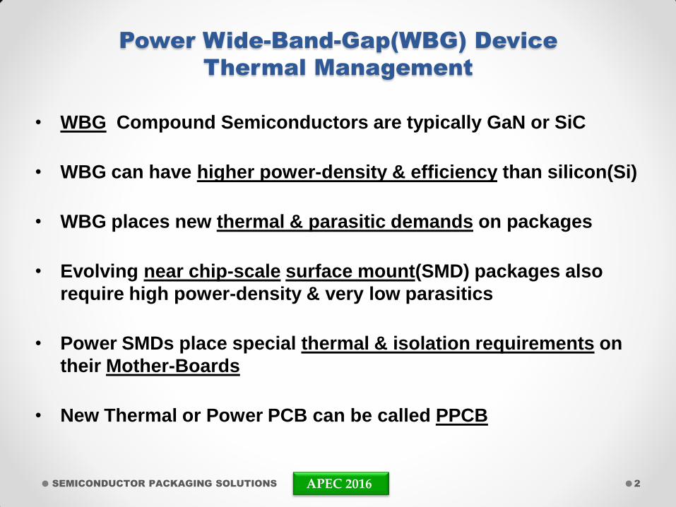
Power Wide-Band-Gap(WBG) Device
Thermal Management
• WBG Compound Semiconductors are typically GaN or SiC
• WBG can have higher power-density & efficiency than silicon(Si)
• WBG places new thermal & parasitic demands on packages
• Evolving near chip-scale surface mount(SMD) packages also
require high power-density & very low parasitics
• Power SMDs place special thermal & isolation requirements on
their Mother-Boards
• New Thermal or Power PCB can be called PPCB
SEMICONDUCTOR PACKAGING SOLUTIONS 2
APEC 2016
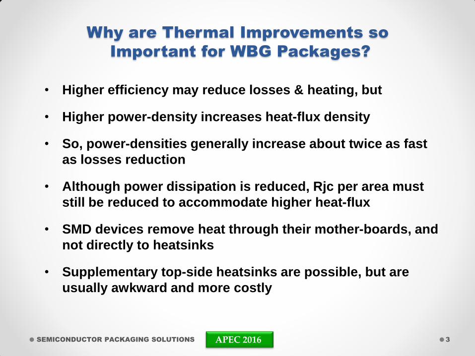
Why are Thermal Improvements so
Important for WBG Packages?
• Higher efficiency may reduce losses & heating, but
• Higher power-density increases heat-flux density
• So, power-densities generally increase about twice as fast
as losses reduction
• Although power dissipation is reduced, Rjc per area must
still be reduced to accommodate higher heat-flux
• SMD devices remove heat through their mother-boards, and
not directly to heatsinks
• Supplementary top-side heatsinks are possible, but are
usually awkward and more costly
SEMICONDUCTOR PACKAGING SOLUTIONS 3
APEC 2016
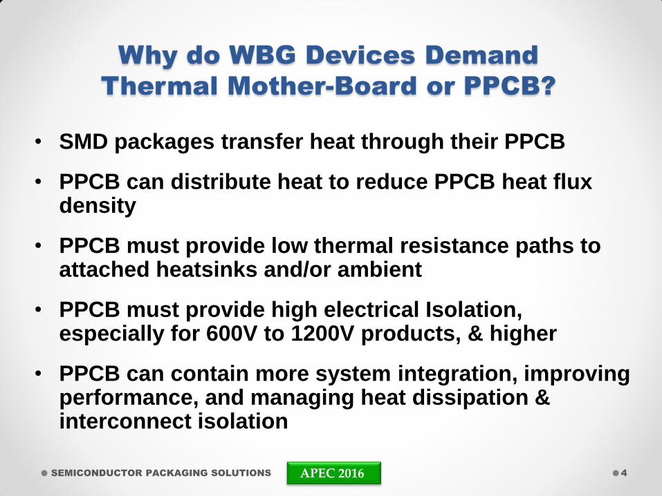
Why do WBG Devices Demand
Thermal Mother-Board or PPCB?
• SMD packages transfer heat through their PPCB
• PPCB can distribute heat to reduce PPCB heat flux density
• PPCB must provide low thermal resistance paths to attached heatsinks and/or ambient
• PPCB must provide high electrical Isolation, especially for 600V to 1200V products, & higher
• PPCB can contain more system integration, improving performance, and managing heat dissipation & interconnect isolation
SEMICONDUCTOR PACKAGING SOLUTIONS 4
APEC 2016
Traditional Si MOSFET & IGBT Power-Packages
Do Not Enable Full WBG Device Performance
Historically
• Too large, complex & expensive
• Require large high R & L internal & external leads & terminals
• Contained many internal high R & L wire-bonds
• Electrically connected by PCBs/bus/cables, but thermally
connected to heatsinks, and both by mechanical screws
• Hard-tooled, expensive, and difficult to customize & optimize
Today
• Their size & parasitics limit power WBG device power-density
speed, performance & efficiency
• Unacceptable for evolving high-performance power WBG devices
SEMICONDUCTOR PACKAGING SOLUTIONS 5
APEC 2016
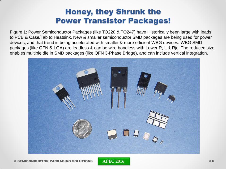
Honey, they Shrunk the
Power Transistor Packages!
Figure 1: Power Semiconductor Packages (like TO220 & TO247) have Historically been large with leads
to PCB & Case/Tab to Heatsink. New & smaller semiconductor SMD packages are being used for power
devices, and that trend is being accelerated with smaller & more efficient WBG devices. WBG SMD
packages (like QFN & LGA) are leadless & can be wire bondless with Lower R, L & Rjc. The reduced size
enables multiple die in SMD packages (like QFN 3-Phase Bridge), and can include vertical integration.
SEMICONDUCTOR PACKAGING SOLUTIONS 6
This photo is a place-holder Final photo will be available in January
APEC 2016
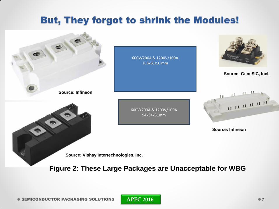
But, They forgot to shrink the Modules!
SEMICONDUCTOR PACKAGING SOLUTIONS 7
Figure 2: These Large Packages are Unacceptable for WBG
600V/200A & 1200V/100A 106x61x31mm
600V/200A & 1200V/100A 94x34x31mm
Source: GeneSIC, Incl.
Source: Infineon
Source: Infineon
Source: Vishay Intertechnologies, Inc.
APEC 2016
Why Shrink the Packages
for Power WBG Packages?
• To improve performance - lower R, L & C
• To enable mobile & miniature applications
• To enable more system integration
• To reduce materials & unit costs
• To reduces tooling costs & equipment costs
• To be flexible - soft-tooling to customize & optimize
• To use existing automatic assembly – commercial
QFN & LGA assembly lines, processes & equipment
• To reduce new product risk & time to market
SEMICONDUCTOR PACKAGING SOLUTIONS 8
APEC 2016
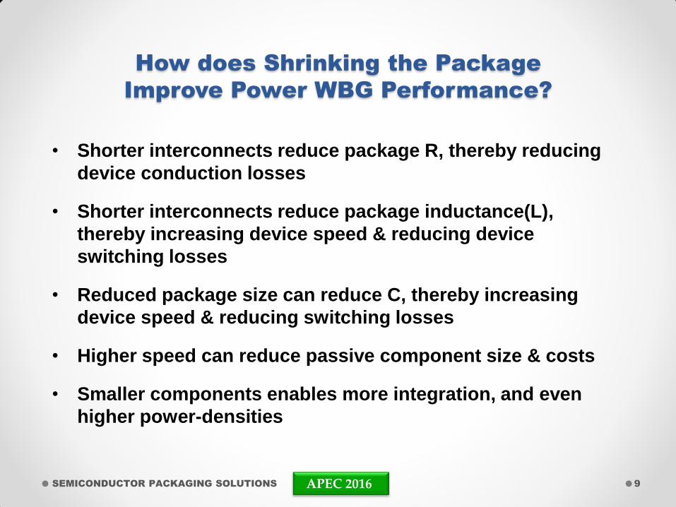
How does Shrinking the Package
Improve Power WBG Performance?
• Shorter interconnects reduce package R, thereby reducing
device conduction losses
• Shorter interconnects reduce package inductance(L),
thereby increasing device speed & reducing device
switching losses
• Reduced package size can reduce C, thereby increasing
device speed & reducing switching losses
• Higher speed can reduce passive component size & costs
• Smaller components enables more integration, and even
higher power-densities
SEMICONDUCTOR PACKAGING SOLUTIONS 9
APEC 2016
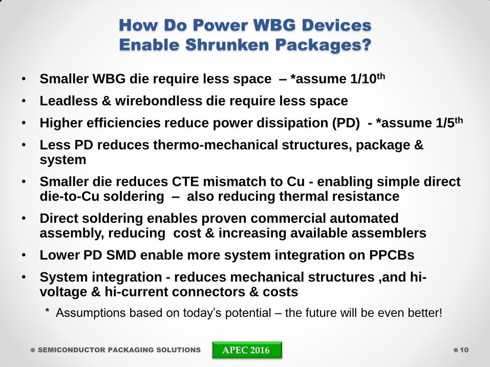
How Do Power WBG Devices
Enable Shrunken Packages?
• Smaller WBG die require less space – *assume 1/10th
• Leadless & wirebondless die require less space
• Higher efficiencies reduce power dissipation (PD) - *assume 1/5th
• Less PD reduces thermo-mechanical structures, package & system
• Smaller die reduces CTE mismatch to Cu - enabling simple direct die-to-Cu soldering – also reducing thermal resistance
• Direct soldering enables proven commercial automated assembly, reducing cost & increasing available assemblers
• Lower PD SMD enable more system integration on PPCBs
• System integration - reduces mechanical structures ,and hi-voltage & hi-current connectors & costs
* Assumptions based on today’s potential – the future will be even better!
SEMICONDUCTOR PACKAGING SOLUTIONS 10

APEC 2016
Package Type Siz
e
SM
D
Lead
less
Wir
eb
on
dle
ss
Resis
tan
ce
Ind
ucta
nce
Rjc
Reli
ab
ilit
y
Co
st
Man
ufa
ctu
rin
g
To
oli
ng
Inte
gra
tio
n*
TO220/TO247 P No No No O U O O P P P P
BGA/LGA G Yes Yes No O P P E E E E P
QFN/DFN G Yes Yes No O P G E E E E P
PLGA G Yes Yes Yes G O G O P P O P
PQFN/PDFN G Yes Yes Yes E G E O P P O P
LGA-Embedded E Yes Yes Yes G E E E O E G E+
LGA-Cavity E Yes Yes Yes G E E E E E E E
QFN/DFN-Cavity E Yes Yes Yes E E+ E+ E E E E G
Abbreviations: E - Excellent P - Poor * Vertical Integrate
G - Good U - Unacceptble
O - Okay
Current & Evolving Power WBG Packages
with Bench-Mark products encircled in Red
SEMICONDUCTOR PACKAGING SOLUTIONS 11
Evo
lvin
g
Table 1: WBG Package Comparisons
APEC 2016
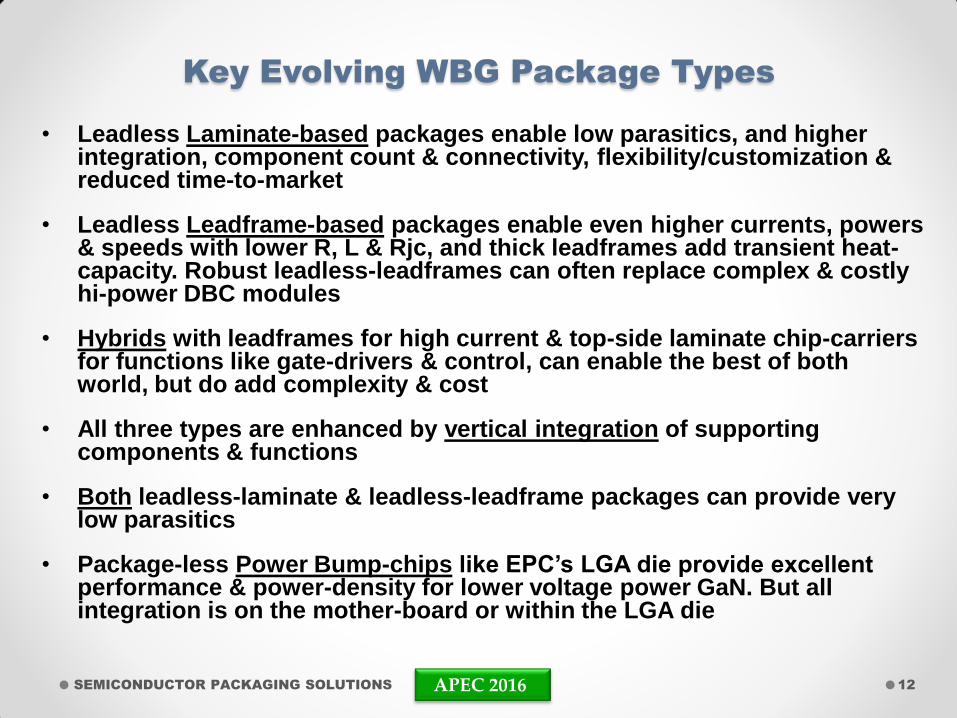
Key Evolving WBG Package Types
• Leadless Laminate-based packages enable low parasitics, and higher integration, component count & connectivity, flexibility/customization & reduced time-to-market
• Leadless Leadframe-based packages enable even higher currents, powers & speeds with lower R, L & Rjc, and thick leadframes add transient heat-capacity. Robust leadless-leadframes can often replace complex & costly hi-power DBC modules
• Hybrids with leadframes for high current & top-side laminate chip-carriers for functions like gate-drivers & control, can enable the best of both world, but do add complexity & cost
• All three types are enhanced by vertical integration of supporting components & functions
• Both leadless-laminate & leadless-leadframe packages can provide very low parasitics
• Package-less Power Bump-chips like EPC’s LGA die provide excellent performance & power-density for lower voltage power GaN. But all integration is on the mother-board or within the LGA die
SEMICONDUCTOR PACKAGING SOLUTIONS 12
APEC 2016
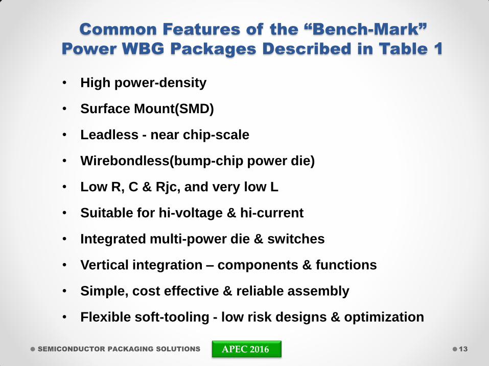
Common Features of the “Bench-Mark”
Power WBG Packages Described in Table 1
• High power-density
• Surface Mount(SMD)
• Leadless - near chip-scale
• Wirebondless(bump-chip power die)
• Low R, C & Rjc, and very low L
• Suitable for hi-voltage & hi-current
• Integrated multi-power die & switches
• Vertical integration – components & functions
• Simple, cost effective & reliable assembly
• Flexible soft-tooling - low risk designs & optimization
SEMICONDUCTOR PACKAGING SOLUTIONS 13
APEC 2016
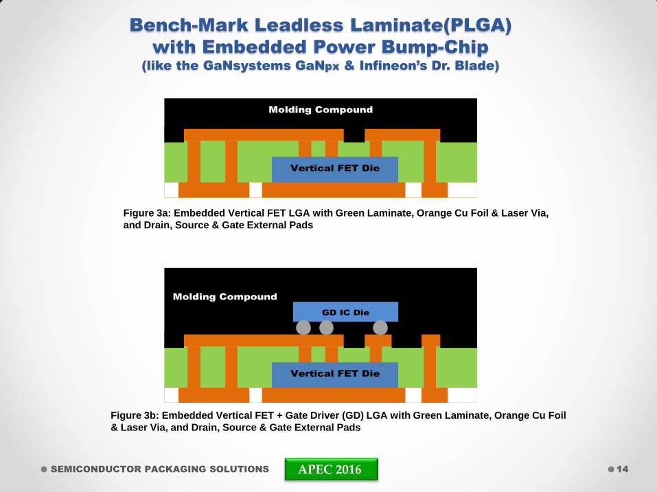
Bench-Mark Leadless Laminate(PLGA)
with Embedded Power Bump-Chip
(like the GaNsystems GaNpx & Infineon’s Dr. Blade)
SEMICONDUCTOR PACKAGING SOLUTIONS 14
Figure 3a: Embedded Vertical FET LGA with Green Laminate, Orange Cu Foil & Laser Via,
and Drain, Source & Gate External Pads
Vertical FET Die
Molding Compound
GD IC Die
Figure 3b: Embedded Vertical FET + Gate Driver (GD) LGA with Green Laminate, Orange Cu Foil
& Laser Via, and Drain, Source & Gate External Pads
Vertical FET Die
Molding Compound
APEC 2016
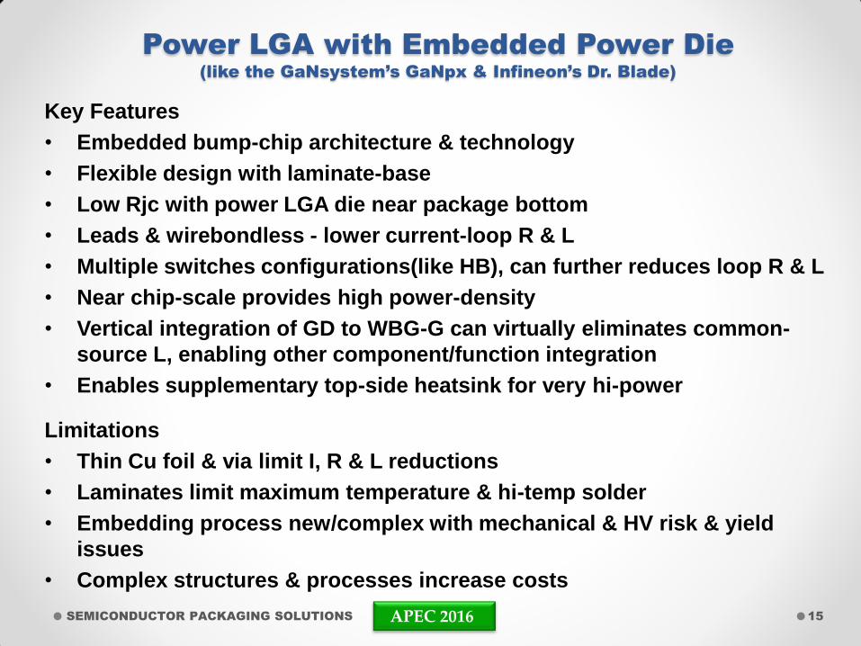
Power LGA with Embedded Power Die
(like the GaNsystem’s GaNpx & Infineon’s Dr. Blade)
Key Features
• Embedded bump-chip architecture & technology
• Flexible design with laminate-base
• Low Rjc with power LGA die near package bottom
• Leads & wirebondless - lower current-loop R & L
• Multiple switches configurations(like HB), can further reduces loop R & L
• Near chip-scale provides high power-density
• Vertical integration of GD to WBG-G can virtually eliminates common-
source L, enabling other component/function integration
• Enables supplementary top-side heatsink for very hi-power
Limitations
• Thin Cu foil & via limit I, R & L reductions
• Laminates limit maximum temperature & hi-temp solder
• Embedding process new/complex with mechanical & HV risk & yield
issues
• Complex structures & processes increase costs
SEMICONDUCTOR PACKAGING SOLUTIONS 15
APEC 2016
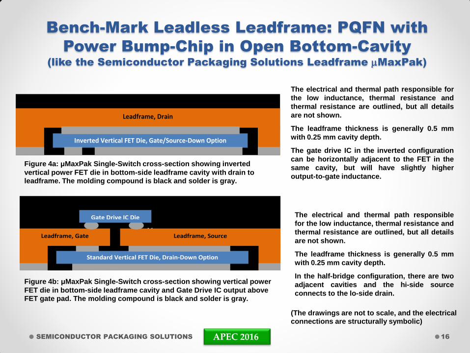
Bench-Mark Leadless Leadframe: PQFN with
Power Bump-Chip in Open Bottom-Cavity
(like the Semiconductor Packaging Solutions Leadframe mMaxPak)
SEMICONDUCTOR PACKAGING SOLUTIONS 16
The electrical and thermal path responsible for
the low inductance, thermal resistance and
thermal resistance are outlined, but all details
are not shown.
The leadframe thickness is generally 0.5 mm
with 0.25 mm cavity depth.
The gate drive IC in the inverted configuration
can be horizontally adjacent to the FET in the
same cavity, but will have slightly higher
output-to-gate inductance.
The electrical and thermal path responsible
for the low inductance, thermal resistance and
thermal resistance are outlined, but all details
are not shown.
The leadframe thickness is generally 0.5 mm
with 0.25 mm cavity depth.
In the half-bridge configuration, there are two
adjacent cavities and the hi-side source
connects to the lo-side drain.
Figure 4a: μMaxPak Single-Switch cross-section showing inverted
vertical power FET die in bottom-side leadframe cavity with drain to leadframe. The molding compound is black and solder is gray.
(The drawings are not to scale, and the electrical connections are structurally symbolic)
Figure 4b: μMaxPak Single-Switch cross-section showing vertical power
FET die in bottom-side leadframe cavity and Gate Drive IC output above FET gate pad. The molding compound is black and solder is gray.
M
Inverted Vertical FET Die, Gate/Source-Down Option
Leadframe, Drain
M
Standard Vertical FET Die, Drain-Down Option
Leadframe, Gate Leadframe, Source
Gate Drive IC Die
APEC 2016
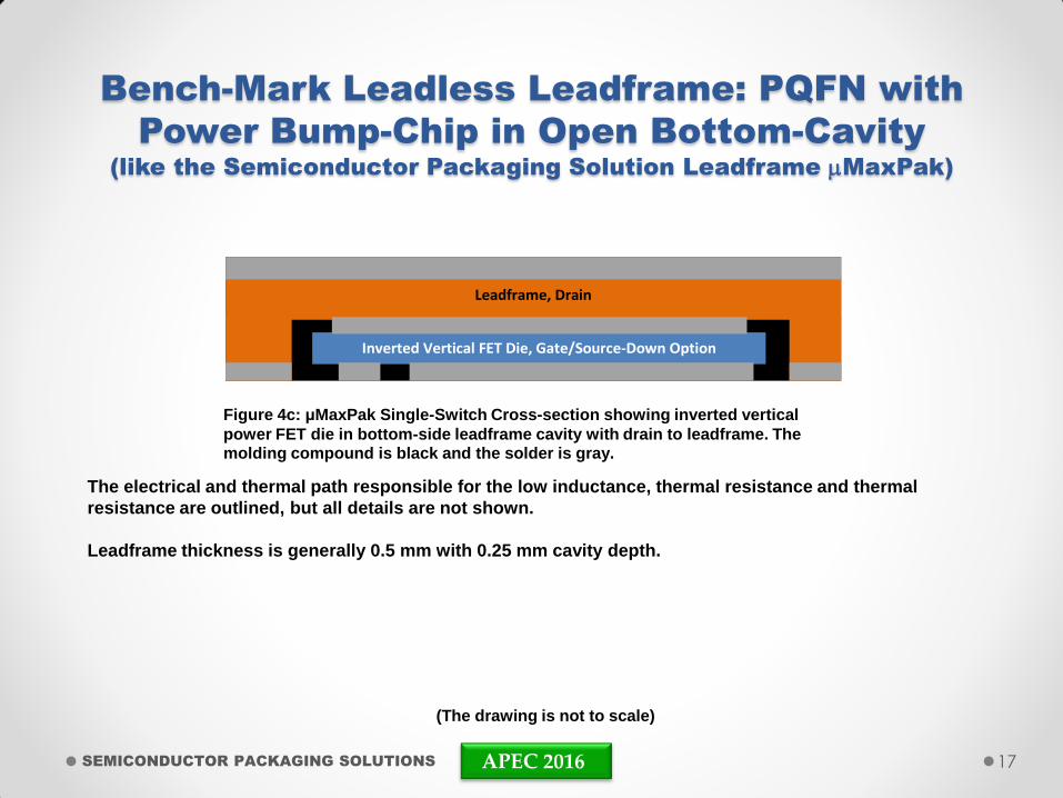
Bench-Mark Leadless Leadframe: PQFN with
Power Bump-Chip in Open Bottom-Cavity
(like the Semiconductor Packaging Solution Leadframe mMaxPak)
17
The electrical and thermal path responsible for the low inductance, thermal resistance and thermal
resistance are outlined, but all details are not shown.
Leadframe thickness is generally 0.5 mm with 0.25 mm cavity depth.
Figure 4c: μMaxPak Single-Switch Cross-section showing inverted vertical
power FET die in bottom-side leadframe cavity with drain to leadframe. The molding compound is black and the solder is gray.
(The drawing is not to scale)
M
Inverted Vertical FET Die, Gate/Source-Down Option
Leadframe, Drain
SEMICONDUCTOR PACKAGING SOLUTIONS
APEC 2016
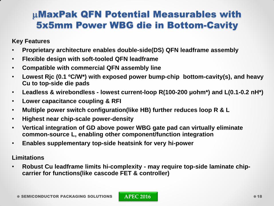
mMaxPak QFN Potential Measurables with
5x5mm Power WBG die in Bottom-Cavity
Key Features
• Proprietary architecture enables double-side(DS) QFN leadframe assembly
• Flexible design with soft-tooled QFN leadframe
• Compatible with commercial QFN assembly line
• Lowest Rjc (0.1 ºC/W*) with exposed power bump-chip bottom-cavity(s), and heavy Cu to top-side die pads
• Leadless & wirebondless - lowest current-loop R(100-200 μohm*) and L(0.1-0.2 nH*)
• Lower capacitance coupling & RFI
• Multiple power switch configuration(like HB) further reduces loop R & L
• Highest near chip-scale power-density
• Vertical integration of GD above power WBG gate pad can virtually eliminate common-source L, enabling other component/function integration
• Enables supplementary top-side heatsink for very hi-power
Limitations
• Robust Cu leadframe limits hi-complexity - may require top-side laminate chip-carrier for functions(like cascode FET & controller)
SEMICONDUCTOR PACKAGING SOLUTIONS 18
APEC 2016
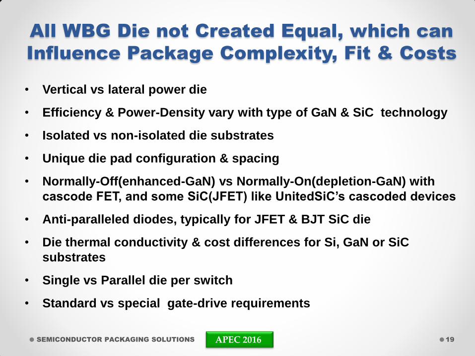
All WBG Die not Created Equal, which can
Influence Package Complexity, Fit & Costs
• Vertical vs lateral power die
• Efficiency & Power-Density vary with type of GaN & SiC technology
• Isolated vs non-isolated die substrates
• Unique die pad configuration & spacing
• Normally-Off(enhanced-GaN) vs Normally-On(depletion-GaN) with
cascode FET, and some SiC(JFET) like UnitedSiC’s cascoded devices
• Anti-paralleled diodes, typically for JFET & BJT SiC die
• Die thermal conductivity & cost differences for Si, GaN or SiC
substrates
• Single vs Parallel die per switch
• Standard vs special gate-drive requirements
SEMICONDUCTOR PACKAGING SOLUTIONS 19
APEC 2016
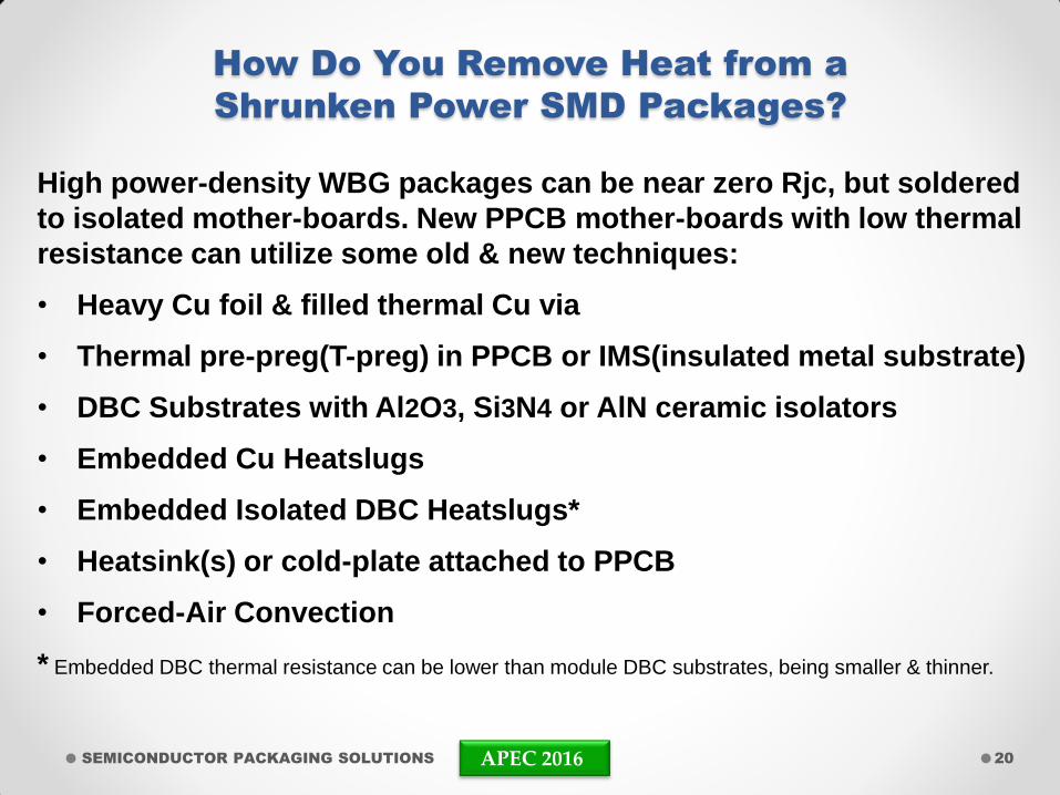
How Do You Remove Heat from a
Shrunken Power SMD Packages?
High power-density WBG packages can be near zero Rjc, but soldered
to isolated mother-boards. New PPCB mother-boards with low thermal
resistance can utilize some old & new techniques:
• Heavy Cu foil & filled thermal Cu via
• Thermal pre-preg(T-preg) in PPCB or IMS(insulated metal substrate)
• DBC Substrates with Al2O3, Si3N4 or AlN ceramic isolators
• Embedded Cu Heatslugs
• Embedded Isolated DBC Heatslugs*
• Heatsink(s) or cold-plate attached to PPCB
• Forced-Air Convection
* Embedded DBC thermal resistance can be lower than module DBC substrates, being smaller & thinner.
SEMICONDUCTOR PACKAGING SOLUTIONS 20
APEC 2016
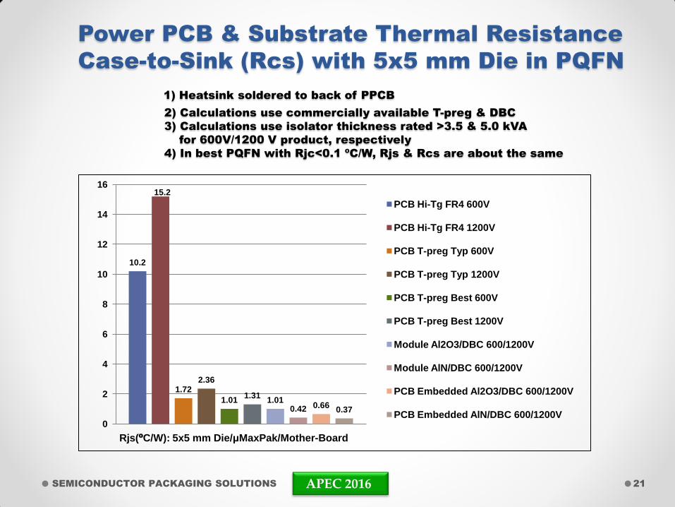
Power PCB & Substrate Thermal Resistance
Case-to-Sink (Rcs) with 5x5 mm Die in PQFN
1) Heatsink soldered to back of PPCB
2) Calculations use commercially available T-preg & DBC
3) Calculations use isolator thickness rated >3.5 & 5.0 kVA
for 600V/1200 V product, respectively
4) In best PQFN with Rjc<0.1 ºC/W, Rjs & Rcs are about the same
SEMICONDUCTOR PACKAGING SOLUTIONS 21
10.2
15.2
1.72 2.36
1.01 1.31
1.01 0.42 0.66
0.37
0
2
4
6
8
10
12
14
16
PCB Hi-Tg FR4 600V
PCB Hi-Tg FR4 1200V
PCB T-preg Typ 600V
PCB T-preg Typ 1200V
PCB T-preg Best 600V
PCB T-preg Best 1200V
Module Al2O3/DBC 600/1200V
Module AlN/DBC 600/1200V
PCB Embedded Al2O3/DBC 600/1200V
PCB Embedded AlN/DBC 600/1200V
Rjs(ºC/W): 5x5 mm Die/μMaxPak/Mother-Board
APEC 2016
High-Speed WBG Devices Require Lower Capacitance to
Heatsink(Ground) at Mother-Board Isolation Layer
• There are compromises between capacitance, thermal resistance & isolation voltage, and product requirements define what is optimum
• C=KA/t, where C=capacitance, K=dielectric constant, A=area & t=thickness
• Increased Thickness - reduces capacitance, increasing thermal resistance & BV
• Typical thickness – T-preg=4mil(3.5KV) & 6mil(5.0KV), Al2O3=20mil(module) & Al2O3=10mil(embedded-LGA) and AlN=25mil(module) & AlN=15mil(embedded-LGA)
• Increased Area – increases capacitance, reducing thermal resistance
• Dielectric Constant - properties of isolation material & frequency. Typical dielectric constants @ 1MHz are T-preg=4.0-7.5, Al2O3=9.0 & AlN=8.5
• WBG die may be 10% Si die area, and leadless & wire bondless embedded isolators area may be 5% the power module DBC area
• Reduced isolator area is a key advantage for New WBG packages & mother-boards with potentially 5% the capacitance die to ground
SEMICONDUCTOR PACKAGING SOLUTIONS 22
APEC 2016
Ultimate Power WBG Packages are:
• Near Chip-Scale - High power-densities
• Leadless & Wire Bondless - Maximum speed & efficiency
• Near-zero Package Rjc - In SMD Packages
• Vertically Integrated - Added functions with even higher power-
density, speed & efficiency
• Used with Power Mother-Boards - Manage HV Isolation & high heat
flux densities to heatsink
• Used with Mother-Board System Integration - Higher product power-
density & performance
• Built on QFN & LGA Platform - Commercial assembly for low cost,
availability, flexible & short time-to-market
SEMICONDUCTOR PACKAGING SOLUTIONS 23