adbs-a350: optical finger navigation chip - · pdf file-a350: optical finger navigation chip...
TRANSCRIPT
1
PixArt Imaging Inc. ADBS-A350 General Datasheet
Optical Finger Navigation Chip
PixArt Imaging Inc. http://www.pixart.com All rights reserved. Any portion in this paper shall not be reproduced, copied, or transformed to any other forms without permission.
Version 1.0 | 05 Sep 2016 | 11010AEN
ADBS-A350: Optical Finger Navigation Chip
Description
The ADBS-A350 chip is a small form factor (SFF) LED illuminated optical finger navigation system. It is designed with low-power architecture and automatic power management modes, making it ideal for battery-and power-sensitive applications such as mobile phones.
The ADBS-A350 is capable of high-speed motion detection– up to 20 ips. In addition, it has an on-chip oscillator and integrated LED to minimize external components. The chip is programmed via registers through either a serial peripheral interface or a two wire interface port.
It is packaged in a 28 I/O surface mountable package. There are no moving parts, thus provide high reliability and less maintenance for the end user. In addition, precision optical alignment is not required, facilitating high volume assembly. The ADBS-A350 is designed for use with ADBL-A321 lens. The ADBL-A321 lens is the optical component necessary for proper operation of the chip.
Theory of Operation
The ADBS-A350 is based on Optical Finger Navigation (OFN) Technology, which measures changes in position by optically acquiring sequential surface images (frames) and mathematically determining the direction and magnitude of movement.
The ADBS-A350 contains an Image Acquisition System (IAS), a Digital Signal Processor (DSP), and a communication system. The IAS acquires microscopic surface images via the lens and illumination system. These images are processed by the DSP to determine the direction and distance of motion. The DSP calculates the Δx and Δy relative displacement values. The host reads the Δx and Δy information from the chip serial port if a motion interrupt is published. The microcontroller then translates the data into cursor navigation, rocker switch, and scrolling or other system dependent navigation data.
Features
Low power architecture Surface mount technology (SMT) device Self-adjusting power-saving modes for longer battery
life High speed motion detection up to 20 ips Self-adjusting frame rate for optimum performance Motion detect interrupt Finger detect interrupt Soft click and Tap detect interrupt Single Interrupt pin Optional PWM output for LED illumination Optional switch input for center click function Internal oscillator – no clock input needed Selectable 125, 250, 500, 750, 1000 and 1250 cpi
resolution
Single 1.8 V supply voltage for analog and digital Internal power up reset (POR) Selectable Input/Output voltage at 1.8 V or 2.8 V
nominal 4-wire Serial peripheral interface (SPI) or Two-wire
interface (TWI)
Integrated chip-on-board LED with wavelength of 870 nm
Applications Finger input devices Mobile devices Integrated input devices Battery-powered input device
Ordering Information
Part Number Type
ADBS-A350 28-pin SMD
ADBL-A321 Lens
PixArt customers purchasing the ADBS-350 OFN product are eligible to receive a royalty free license to our US patents 6977645, 6621483, 6950094, 6172354 and 7289649, for use in their end products.
2 PixArt Imaging Inc. http://www.pixart.com All rights reserved. Any portion in this paper shall not be reproduced, copied, or transformed to any other forms without permission.
Version 1.0 | 05 Sep 2016 | 11010AEN
PixArt Imaging Inc. ADBS-A350 General Datasheet
Optical Finger Navigation Chip
ADBS-A350 General Datasheet Optical Finger Navigation Chip
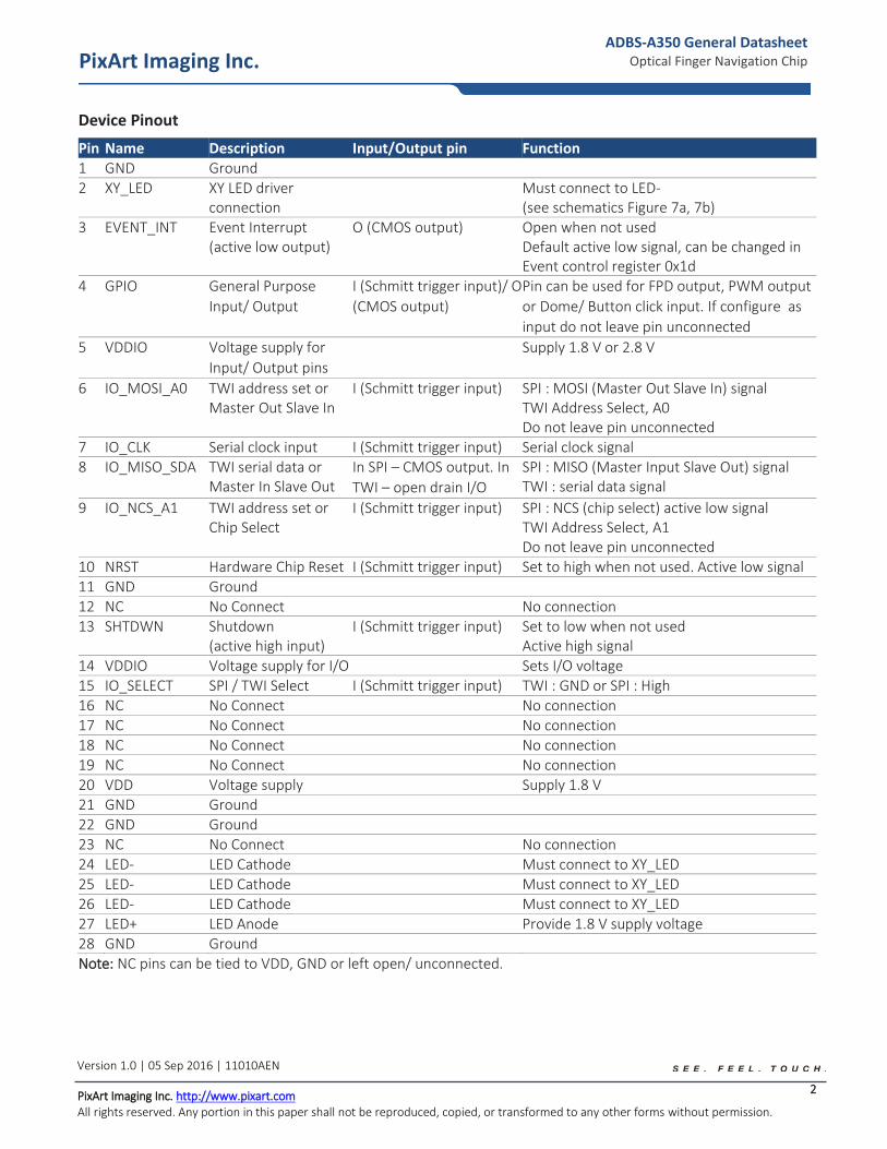
Device Pinout
Pin Name Description Input/Output pin Function 1 GND Ground 2 XY_LED XY LED driver
connection Must connect to LED-
(see schematics Figure 7a, 7b) 3 EVENT_INT Event Interrupt
(active low output) O (CMOS output) Open when not used
Default active low signal, can be changed in Event control register 0x1d
4 GPIO General Purpose
Input/ Output
I (Schmitt trigger input)/ O
(CMOS output)
Pin can be used for FPD output, PWM output
or Dome/ Button click input. If configure as
input do not leave pin unconnected
5 VDDIO Voltage supply for
Input/ Output pins
Supply 1.8 V or 2.8 V
6 IO_MOSI_A0 TWI address set or Master Out Slave In
I (Schmitt trigger input) SPI : MOSI (Master Out Slave In) signal TWI Address Select, A0 Do not leave pin unconnected
7 IO_CLK Serial clock input I (Schmitt trigger input) Serial clock signal 8 IO_MISO_SDA TWI serial data or
Master In Slave Out In SPI – CMOS output. In
TWI – open drain I/O
SPI : MISO (Master Input Slave Out) signal TWI : serial data signal
9 IO_NCS_A1 TWI address set or Chip Select
I (Schmitt trigger input) SPI : NCS (chip select) active low signal TWI Address Select, A1 Do not leave pin unconnected
10 NRST Hardware Chip Reset I (Schmitt trigger input) Set to high when not used. Active low signal 11 GND Ground 12 NC No Connect No connection 13 SHTDWN Shutdown
(active high input) I (Schmitt trigger input) Set to low when not used
Active high signal 14 VDDIO Voltage supply for I/O Sets I/O voltage 15 IO_SELECT SPI / TWI Select I (Schmitt trigger input) TWI : GND or SPI : High 16 NC No Connect No connection 17 NC No Connect No connection 18 NC No Connect No connection 19 NC No Connect No connection 20 VDD Voltage supply Supply 1.8 V 21 GND Ground 22 GND Ground 23 NC No Connect No connection 24 LED- LED Cathode Must connect to XY_LED 25 LED- LED Cathode Must connect to XY_LED 26 LED- LED Cathode Must connect to XY_LED 27 LED+ LED Anode Provide 1.8 V supply voltage 28 GND Ground Note: NC pins can be tied to VDD, GND or left open/ unconnected.
3 PixArt Imaging Inc. http://www.pixart.com All rights reserved. Any portion in this paper shall not be reproduced, copied, or transformed to any other forms without permission.
Version 1.0 | 05 Sep 2016 | 11010AEN
PixArt Imaging Inc. ADBS-A350 General Datasheet
Optical Finger Navigation Chip
ADBS-A350 General Datasheet Optical Finger Navigation Chip
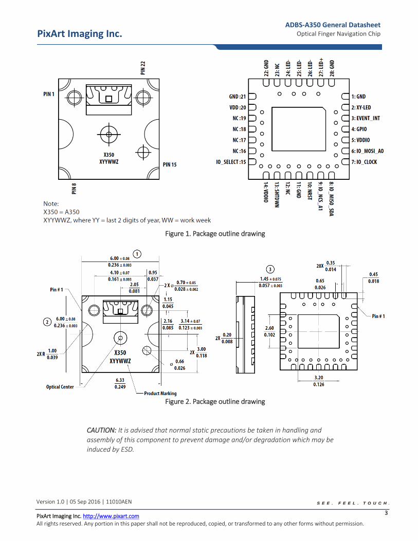
PIN 22
22: GND
23: NC
24: LE
D-
25: LE
D-
26: LE
D-
27: LED+
28: GND
Figure 1. Package outline drawing
Figure 2. Package outline drawing
CAUTION: It is advised that normal static precautions be taken in handling and
assembly of this component to prevent damage and/or degradation which may be
induced by ESD.
4 PixArt Imaging Inc. http://www.pixart.com All rights reserved. Any portion in this paper shall not be reproduced, copied, or transformed to any other forms without permission.
Version 1.0 | 05 Sep 2016 | 11010AEN
PixArt Imaging Inc. ADBS-A350 General Datasheet
Optical Finger Navigation Chip
ADBS-A350 General Datasheet Optical Finger Navigation Chip
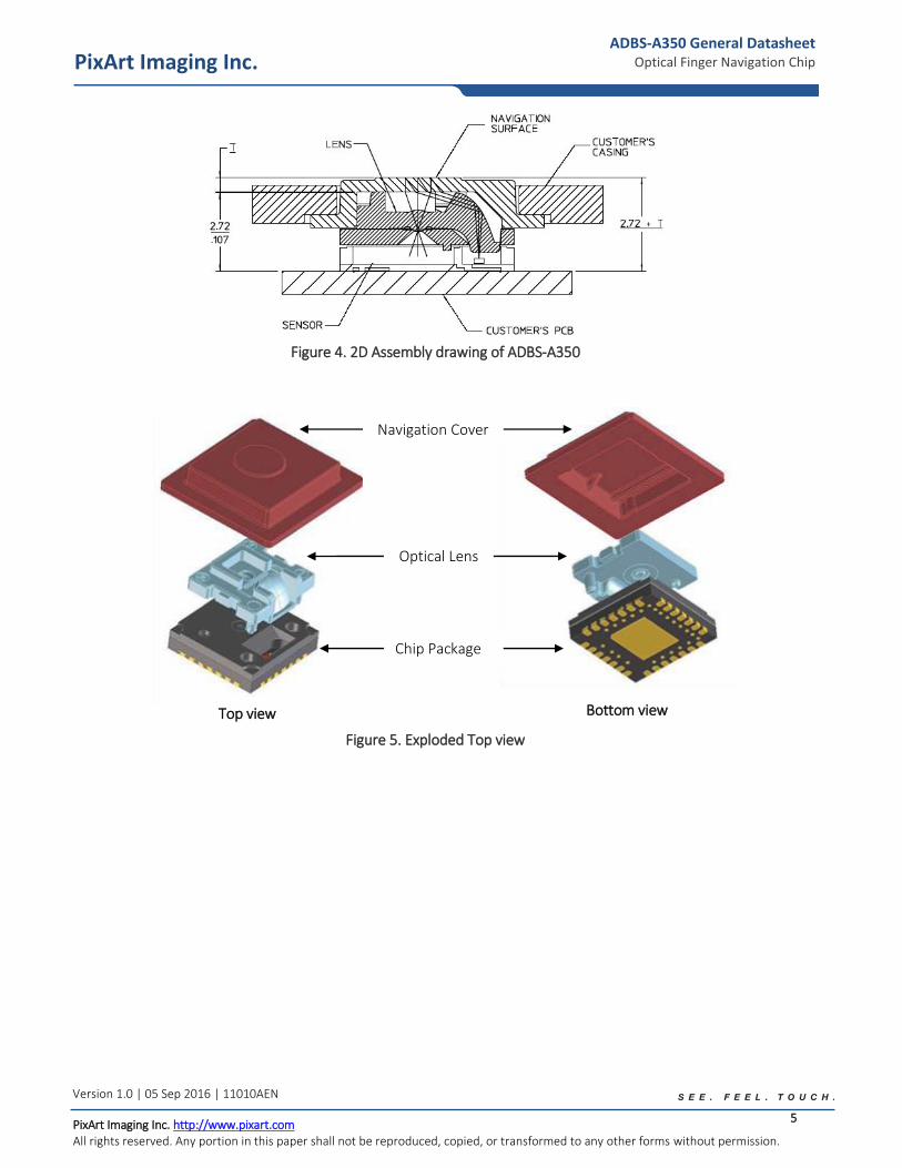
Overview of Optical Chip Assembly
PixArt Imaging provides an IGES file drawing describing the cover plate molding features.
Chip Assembly
The components interlock as they are mounted onto defined features on the cover plate. The ADBS-A350 chip is designed for surface mounting on a PCB, looking up. There is an aperture stop and features on the package that align to the lens.
The lens provides optics for the imaging of the surface as well as illumination of the surface at the optimum angle. Features on the lens align it to the chip and cover plate. Contamination must be kept away from the lens. During assembly process, it is recommended to use a minimum of a 10K clean room environment or equivalent laminar flow workbench.
PCB Assembly Considerations
1. Surface mount the chip and all other electrical components into PCB.
2. Reflow the entire assembly in a no-wash solder process.
3. Remove the protective kapton tape from optical aperture of the chip and LED. Care must be taken to keep contaminants from entering the aperture. Recommend not to place the PCB facing up during the entire assembly process. Recommend to hold the PCB first vertically for the kapton removal process.
4. Press fit the lens onto the chip until there is no gap between the lens and chip, with force up to maximum 2.2 kgf. Care must be taken to avoid contaminating or staining the lens. The lens piece has alignment posts which will mate with the alignment holes on the chip package.
5. Place and secure the optical navigation cover onto the lens to ensure the chip and lens components are always interlocked to the correct vertical height. The cover design has a foolproof feature to avoid wrong orientation of the cover.
6. The optical position reference for the PCB is set by the navigation cover and lens.
7. Install device top casing. There MUST be a feature in either top casing or bottom casing to press onto the chip to ensure the chip and lens components are always interlocked to the correct vertical height.
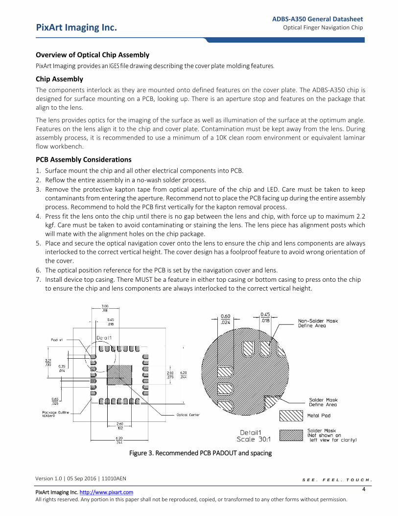
Figure 3. Recommended PCB PADOUT and spacing
5 PixArt Imaging Inc. http://www.pixart.com All rights reserved. Any portion in this paper shall not be reproduced, copied, or transformed to any other forms without permission.
Version 1.0 | 05 Sep 2016 | 11010AEN
PixArt Imaging Inc. ADBS-A350 General Datasheet
Optical Finger Navigation Chip
ADBS-A350 General Datasheet Optical Finger Navigation Chip
Figure 4. 2D Assembly drawing of ADBS-A350
Figure 5. Exploded Top view
Navigation Cover
Optical Lens
Chip Package
Top view Bottom view
6 PixArt Imaging Inc. http://www.pixart.com All rights reserved. Any portion in this paper shall not be reproduced, copied, or transformed to any other forms without permission.
Version 1.0 | 05 Sep 2016 | 11010AEN
PixArt Imaging Inc. ADBS-A350 General Datasheet
Optical Finger Navigation Chip
ADBS-A350 General Datasheet Optical Finger Navigation Chip
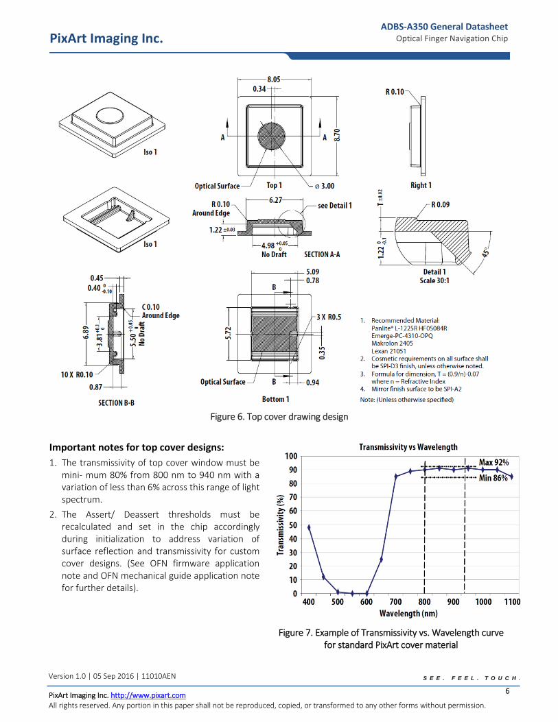
Figure 6. Top cover drawing design
Important notes for top cover designs:
1. The transmissivity of top cover window must be mini- mum 80% from 800 nm to 940 nm with a variation of less than 6% across this range of light spectrum.
2. The Assert/ Deassert thresholds must be recalculated and set in the chip accordingly during initialization to address variation of surface reflection and transmissivity for custom cover designs. (See OFN firmware application note and OFN mechanical guide application note for further details).
Figure 7. Example of Transmissivity vs. Wavelength curve for standard PixArt cover material
7 PixArt Imaging Inc. http://www.pixart.com All rights reserved. Any portion in this paper shall not be reproduced, copied, or transformed to any other forms without permission.
Version 1.0 | 05 Sep 2016 | 11010AEN
PixArt Imaging Inc. ADBS-A350 General Datasheet
Optical Finger Navigation Chip
ADBS-A350 General Datasheet Optical Finger Navigation Chip
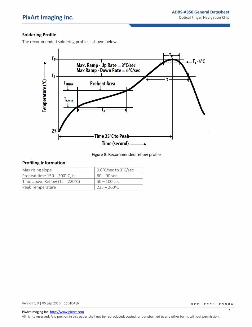
Soldering Profile
The recommended soldering profile is shown below.
Figure 8. Recommended reflow profile
Profiling Information
Max rising slope 0.0°C/sec to 3°C/sec
Preheat time 150 – 200° C, ts 60 – 90 sec
Time above Reflow (TL = 220°C) 50 – 100 sec
Peak Temperature 225 – 260°C
8 PixArt Imaging Inc. http://www.pixart.com All rights reserved. Any portion in this paper shall not be reproduced, copied, or transformed to any other forms without permission.
Version 1.0 |22 Jan 2016 | 11010AEN
PixArt Imaging Inc. ADBS-A350 General Datasheet
Optical Finger Navigation Chip
ADBS-A350 General Datasheet Optical Finger Navigation Chip
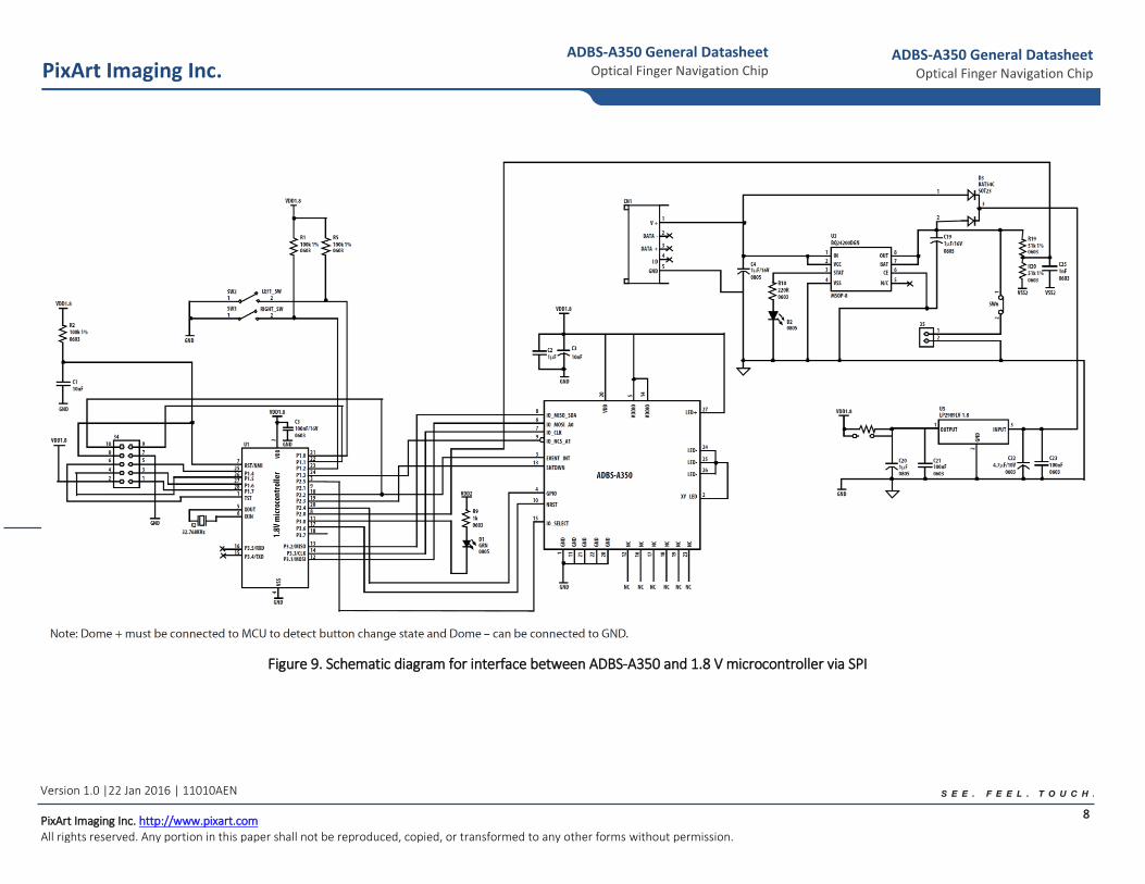
Figure 9. Schematic diagram for interface between ADBS-A350 and 1.8 V microcontroller via SPI
9
PixArt Imaging Inc. ADBS-A350 General Datasheet
Optical Finger Navigation Chip
ADBS-A350 General Datasheet Optical Finger Navigation Chip
PixArt Imaging Inc. http://www.pixart.com All rights reserved. Any portion in this paper shall not be reproduced, copied, or transformed to any other forms without permission.
Version 1.0 |22 Jan 2016 | 11010AEN
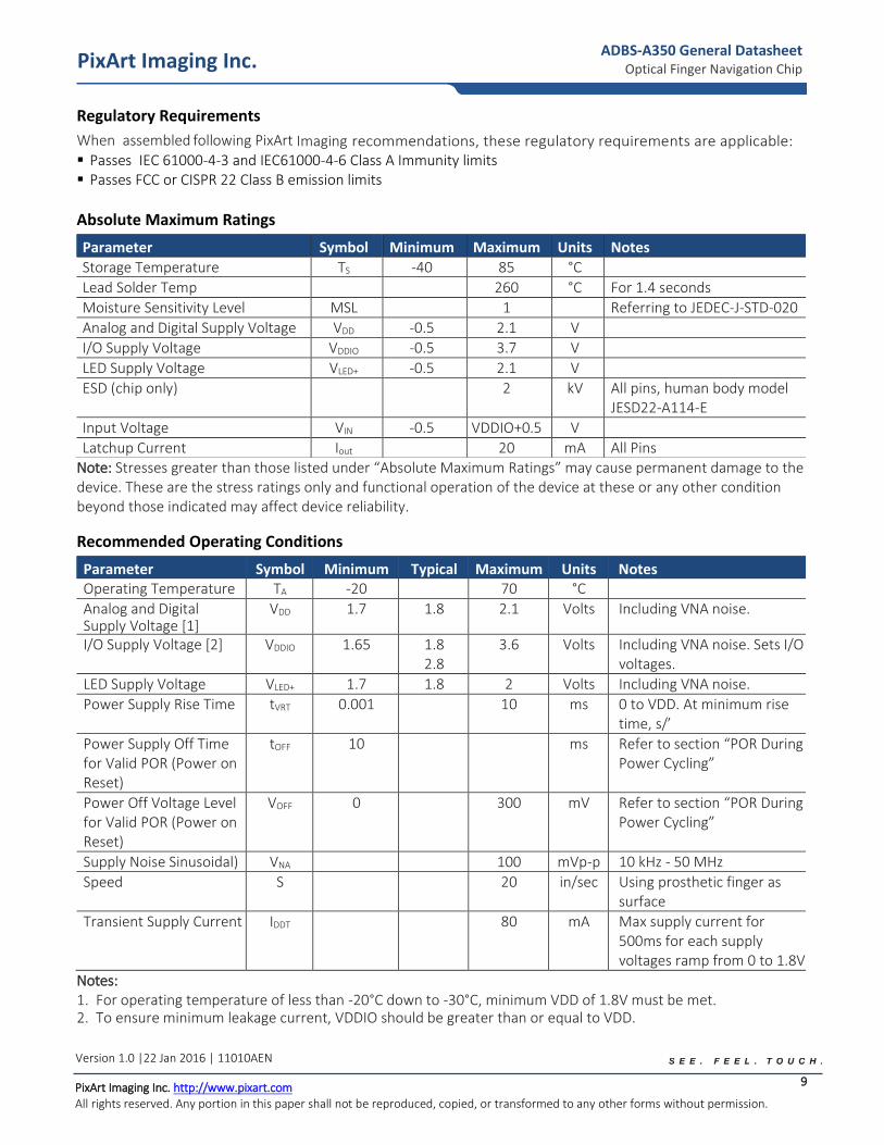
Regulatory Requirements
When assembled following PixArt Imaging recommendations, these regulatory requirements are applicable: Passes IEC 61000-4-3 and IEC61000-4-6 Class A Immunity limits Passes FCC or CISPR 22 Class B emission limits
Absolute Maximum Ratings
Parameter Symbol Minimum Maximum Units Notes Storage Temperature TS -40 85 °C
Lead Solder Temp 260 °C For 1.4 seconds
Moisture Sensitivity Level MSL 1 Referring to JEDEC-J-STD-020
Analog and Digital Supply Voltage VDD -0.5 2.1 V
I/O Supply Voltage VDDIO -0.5 3.7 V
LED Supply Voltage VLED+ -0.5 2.1 V
ESD (chip only) 2 kV All pins, human body model JESD22-A114-E
Input Voltage VIN -0.5 VDDIO+0.5 V
Latchup Current Iout 20 mA All Pins Note: Stresses greater than those listed under “Absolute Maximum Ratings” may cause permanent damage to the device. These are the stress ratings only and functional operation of the device at these or any other condition beyond those indicated may affect device reliability. Recommended Operating Conditions
Parameter Symbol Minimum Typical Maximum Units Notes Operating Temperature TA -20 70 °C
Analog and Digital Supply Voltage [1]
VDD 1.7 1.8 2.1 Volts Including VNA noise.
I/O Supply Voltage [2] VDDIO 1.65 1.8 2.8
3.6 Volts Including VNA noise. Sets I/O voltages.
LED Supply Voltage VLED+ 1.7 1.8 2 Volts Including VNA noise.
Power Supply Rise Time tVRT 0.001 10 ms 0 to VDD. At minimum rise time, s/’
Power Supply Off Time for Valid POR (Power on Reset)
tOFF 10 ms Refer to section “POR During Power Cycling”
Power Off Voltage Level for Valid POR (Power on Reset)
VOFF 0 300 mV Refer to section “POR During Power Cycling”
Supply Noise Sinusoidal) VNA 100 mVp-p 10 kHz - 50 MHz
Speed S 20 in/sec Using prosthetic finger as surface
Transient Supply Current IDDT 80 mA Max supply current for 500ms for each supply voltages ramp from 0 to 1.8V
Notes: 1. For operating temperature of less than -20°C down to -30°C, minimum VDD of 1.8V must be met. 2. To ensure minimum leakage current, VDDIO should be greater than or equal to VDD.
10
PixArt Imaging Inc. ADBS-A350 General Datasheet
Optical Finger Navigation Chip
ADBS-A350 General Datasheet Optical Finger Navigation Chip
PixArt Imaging Inc. http://www.pixart.com All rights reserved. Any portion in this paper shall not be reproduced, copied, or transformed to any other forms without permission.
Version 1.0 |22 Jan 2016 | 11010AEN
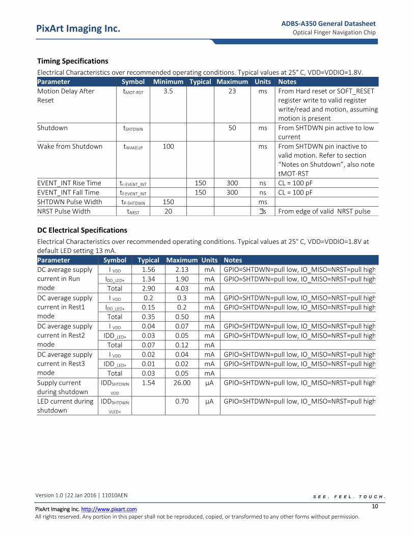
Timing Specifications
Electrical Characteristics over recommended operating conditions. Typical values at 25° C, VDD=VDDIO=1.8V. Parameter Symbol Minimum Typical Maximum Units Notes
Motion Delay After Reset
tMOT-RST 3.5 23 ms From Hard reset or SOFT_RESET register write to valid register write/read and motion, assuming motion is present
Shutdown tSHTDWN 50 ms From SHTDWN pin active to low current
Wake from Shutdown tWAKEUP 100 ms From SHTDWN pin inactive to valid motion. Refer to section “Notes on Shutdown”, also note tMOT-RST
EVENT_INT Rise Time tr-EVENT_INT 150 300 ns CL = 100 pF
EVENT_INT Fall Time tf-EVENT_INT 150 300 ns CL = 100 pF
SHTDWN Pulse Width tP-SHTDWN 150 ms
NRST Pulse Width tNRST 20 s From edge of valid NRST pulse
DC Electrical Specifications
Electrical Characteristics over recommended operating conditions. Typical values at 25° C, VDD=VDDIO=1.8V at default LED setting 13 mA.
Parameter Symbol Typical Maximum Units Notes
DC average supply current in Run mode
I VDD 1.56 2.13 mA GPIO=SHTDWN=pull low, IO_MISO=NRST=pull high.
IDD_LED+ 1.34 1.90 mA GPIO=SHTDWN=pull low, IO_MISO=NRST=pull high.
Total 2.90 4.03 mA
DC average supply current in Rest1 mode
I VDD 0.2 0.3 mA GPIO=SHTDWN=pull low, IO_MISO=NRST=pull high.
IDD_LED+ 0.15 0.2 mA GPIO=SHTDWN=pull low, IO_MISO=NRST=pull high.
Total 0.35 0.50 mA
DC average supply current in Rest2 mode
I VDD 0.04 0.07 mA GPIO=SHTDWN=pull low, IO_MISO=NRST=pull high.
IDD_LED+ 0.03 0.05 mA GPIO=SHTDWN=pull low, IO_MISO=NRST=pull high.
Total 0.07 0.12 mA
DC average supply current in Rest3 mode
I VDD 0.02 0.04 mA GPIO=SHTDWN=pull low, IO_MISO=NRST=pull high.
IDD_LED+ 0.01 0.02 mA GPIO=SHTDWN=pull low, IO_MISO=NRST=pull high.
Total 0.03 0.05 mA
Supply current during shutdown
IDDSHTDWN
VDD 1.54 26.00 µA GPIO=SHTDWN=pull low, IO_MISO=NRST=pull high.
LED current during shutdown
IDDSHTDWN
VLED+
0.70 µA GPIO=SHTDWN=pull low, IO_MISO=NRST=pull high.
11
PixArt Imaging Inc. ADBS-A350 General Datasheet
Optical Finger Navigation Chip
ADBS-A350 General Datasheet Optical Finger Navigation Chip
PixArt Imaging Inc. http://www.pixart.com All rights reserved. Any portion in this paper shall not be reproduced, copied, or transformed to any other forms without permission.
Version 1.0 |22 Jan 2016 | 11010AEN
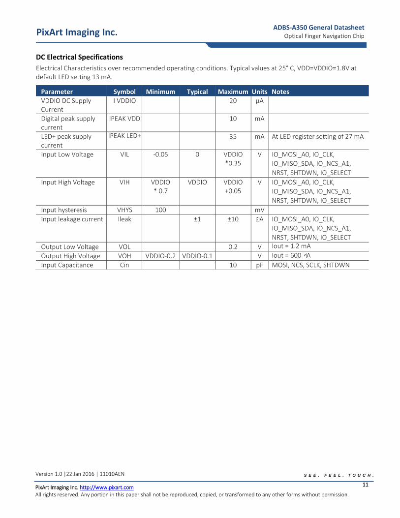
DC Electrical Specifications
Electrical Characteristics over recommended operating conditions. Typical values at 25° C, VDD=VDDIO=1.8V at default LED setting 13 mA.
Parameter Symbol Minimum Typical Maximum Units Notes VDDIO DC Supply Current
I VDDIO 20 µA
Digital peak supply current
IPEAK VDD 10 mA
LED+ peak supply current
IPEAK LED+ 35 mA At LED register setting of 27 mA
Input Low Voltage VIL -0.05 0 VDDIO *0.35
V IO_MOSI_A0, IO_CLK,
IO_MISO_SDA, IO_NCS_A1,
NRST, SHTDWN, IO_SELECT
Input High Voltage VIH VDDIO * 0.7
VDDIO VDDIO +0.05
V IO_MOSI_A0, IO_CLK,
IO_MISO_SDA, IO_NCS_A1,
NRST, SHTDWN, IO_SELECT
Input hysteresis VHYS 100 mV
Input leakage current Ileak ±1 ±10 A IO_MOSI_A0, IO_CLK,
IO_MISO_SDA, IO_NCS_A1,
NRST, SHTDWN, IO_SELECT
Output Low Voltage VOL 0.2 V Iout = 1.2 mA
Output High Voltage VOH VDDIO-0.2 VDDIO-0.1 V Iout = 600 A
Input Capacitance Cin 10 pF MOSI, NCS, SCLK, SHTDWN
12
PixArt Imaging Inc. ADBS-A350 General Datasheet
Optical Finger Navigation Chip
ADBS-A350 General Datasheet Optical Finger Navigation Chip
PixArt Imaging Inc. http://www.pixart.com All rights reserved. Any portion in this paper shall not be reproduced, copied, or transformed to any other forms without permission.
Version 1.0 |22 Jan 2016 | 11010AEN
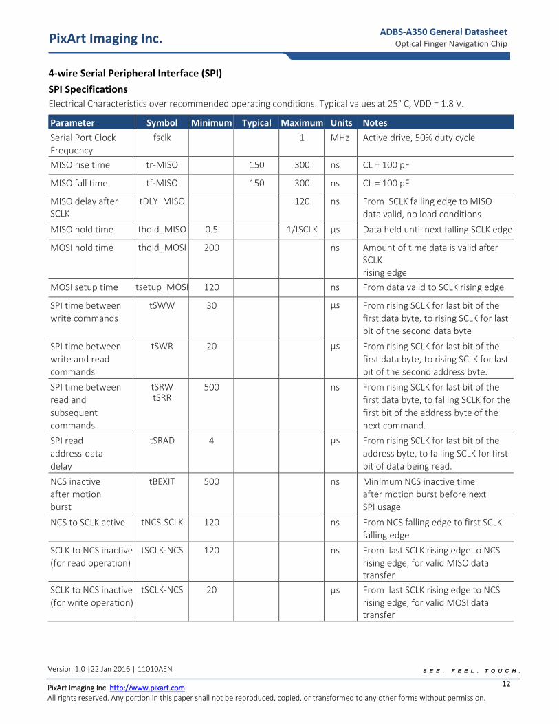
4-wire Serial Peripheral Interface (SPI)
SPI Specifications
Electrical Characteristics over recommended operating conditions. Typical values at 25° C, VDD = 1.8 V.
Parameter Symbol Minimum Typical Maximum Units Notes
Serial Port Clock
Frequency
fsclk 1 MHz Active drive, 50% duty cycle
MISO rise time tr-MISO 150 300 ns CL = 100 pF
MISO fall time tf-MISO 150 300 ns CL = 100 pF
MISO delay after SCLK
tDLY_MISO 120 ns From SCLK falling edge to MISO
data valid, no load conditions
MISO hold time thold_MISO 0.5 1/fSCLK μs Data held until next falling SCLK edge
MOSI hold time thold_MOSI 200 ns Amount of time data is valid after SCLK
rising edge
MOSI setup time tsetup_MOSI 120 ns From data valid to SCLK rising edge
SPI time between
write commands
tSWW 30 µs From rising SCLK for last bit of the
first data byte, to rising SCLK for last
bit of the second data byte
SPI time between
write and read
commands
tSWR 20 µs From rising SCLK for last bit of the
first data byte, to rising SCLK for last
bit of the second address byte.
SPI time between
read and
subsequent
commands
tSRW tSRR
500 ns From rising SCLK for last bit of the
first data byte, to falling SCLK for the
first bit of the address byte of the
next command.
SPI read
address-data
delay
tSRAD 4 µs From rising SCLK for last bit of the
address byte, to falling SCLK for first
bit of data being read.
NCS inactive
after motion
burst
tBEXIT 500 ns Minimum NCS inactive time
after motion burst before next
SPI usage
NCS to SCLK active tNCS-SCLK 120 ns From NCS falling edge to first SCLK
falling edge
SCLK to NCS inactive
(for read operation)
tSCLK-NCS 120 ns From last SCLK rising edge to NCS
rising edge, for valid MISO data transfer
SCLK to NCS inactive
(for write operation)
tSCLK-NCS 20 µs From last SCLK rising edge to NCS
rising edge, for valid MOSI data transfer
13
PixArt Imaging Inc. ADBS-A350 General Datasheet
Optical Finger Navigation Chip
ADBS-A350 General Datasheet Optical Finger Navigation Chip
PixArt Imaging Inc. http://www.pixart.com All rights reserved. Any portion in this paper shall not be reproduced, copied, or transformed to any other forms without permission.
Version 1.0 |22 Jan 2016 | 11010AEN
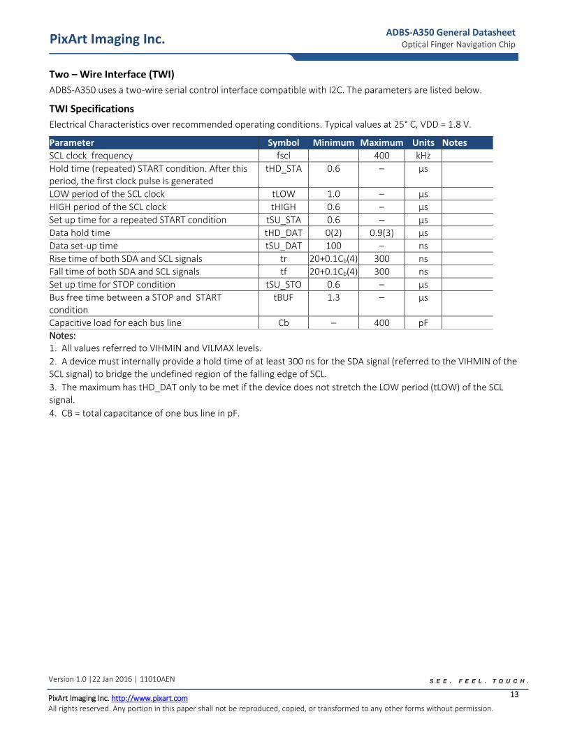
Two – Wire Interface (TWI)
ADBS-A350 uses a two-wire serial control interface compatible with I2C. The parameters are listed below.
TWI Specifications
Electrical Characteristics over recommended operating conditions. Typical values at 25° C, VDD = 1.8 V.
Parameter Symbol Minimum Maximum Units Notes
SCL clock frequency fscl 400 kHz
Hold time (repeated) START condition. After this period, the first clock pulse is generated
tHD_STA 0.6 – µs
LOW period of the SCL clock tLOW 1.0 – µs
HIGH period of the SCL clock tHIGH 0.6 – µs
Set up time for a repeated START condition tSU_STA 0.6 – µs
Data hold time tHD_DAT 0(2) 0.9(3) µs
Data set-up time tSU_DAT 100 – ns
Rise time of both SDA and SCL signals tr 20+0.1Cb(4) 300 ns
Fall time of both SDA and SCL signals tf 20+0.1Cb(4) 300 ns
Set up time for STOP condition tSU_STO 0.6 – µs
Bus free time between a STOP and START condition
tBUF 1.3 – µs
Capacitive load for each bus line Cb – 400 pF Notes: 1. All values referred to VIHMIN and VILMAX levels.
2. A device must internally provide a hold time of at least 300 ns for the SDA signal (referred to the VIHMIN of the SCL signal) to bridge the undefined region of the falling edge of SCL.
3. The maximum has tHD_DAT only to be met if the device does not stretch the LOW period (tLOW) of the SCL signal.
4. CB = total capacitance of one bus line in pF.
14
PixArt Imaging Inc. ADBS-A350 General Datasheet
Optical Finger Navigation Chip
ADBS-A350 General Datasheet Optical Finger Navigation Chip
PixArt Imaging Inc. http://www.pixart.com All rights reserved. Any portion in this paper shall not be reproduced, copied, or transformed to any other forms without permission.
Version 1.0 |22 Jan 2016 | 11010AEN
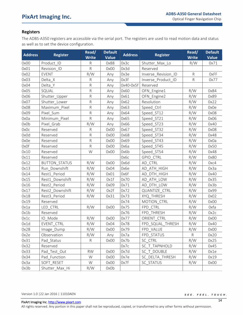
Registers
The ADBS-A350 registers are accessible via the serial port. The registers are used to read motion data and status
as well as to set the device configuration.
Address Register Read/ Write
Default Value
Address Register Read/ Write
Default Value
0x00 Product_ID R 0x88 0x3c Shutter_Max_Lo R/W 0x71
0x01 Revision_ID R 0x00 0x3d Reserved
0x02 EVENT R/W Any 0x3e Inverse_Revision_ID R 0xFF
0x03 Delta_X R Any 0x3f Inverse_Product_ID R 0x77
0x04 Delta_Y R Any 0x40-0x5f Reserved
0x05 SQUAL R Any 0x60 OFN_Engine1 R/W 0x84
0x06 Shutter_Upper R Any 0x61 OFN_Engine2 R/W 0x89
0x07 Shutter_Lower R Any 0x62 Resolution R/W 0x22
0x08 Maximum_Pixel R Any 0x63 Speed_Ctrl R/W 0x0e
0x09 Pixel_Sum R Any 0x64 Speed_ST12 R/W 0x08
0x0a Minimum_Pixel R Any 0x65 Speed_ST21 R/W 0x06
0x0b Pixel_Grab R/W Any 0x66 Speed_ST23 R/W 0x40
0x0c Reserved R 0x00 0x67 Speed_ST32 R/W 0x08
0x0d Reserved R 0x00 0x68 Speed_ST34 R/W 0x48
0x0e Reserved R 0x00 0x69 Speed_ST43 R/W 0x0a
0x0f Reserved R 0x00 0x6a Speed_ST45 R/W 0x50
0x10 Reserved W 0x00 0x6b Speed_ST54 R/W 0x48
0x11 Reserved 0x6c GPIO_CTRL R/W 0x80
0x12 BUTTON_STATUS R/W 0x00 0x6d AD_CTRL R/W 0xc4
0x13 Run_Downshift R/W 0x04 0x6e AD_ATH_HIGH R/W 0x3a
0x14 Rest1_Period R/W 0x01 0x6f AD_DTH_HIGH R/W 0x40
0x15 Rest1_Downshift R/W 0x1f 0x70 AD_ATH_LOW R/W 0x35
0x16 Rest2_Period R/W 0x09 0x71 AD_DTH_LOW R/W 0x3b
0x17 Rest2_Downshift R/W 0x2f 0x72 QUANTIZE_CTRL R/W 0x99
0x18 Rest3_Period R/W 0x31 0x73 XYQ_THRESH R/W 0x02
0x19 Reserved 0x74 MOTION_CTRL R/W 0x00
0x1a LED_CTRL R/W 0x00 0x75 FPD_CTRL R/W 0xfa
0x1b Reserved 0x76 FPD_THRESH R/W 0x2c
0x1c IO_Mode R/W 0x00 0x77 ORIENT_CTRL R/W 0x00
0x1d EVENT_CTRL R/W 0x04 0x78 FPD_SQUAL_THRESH R/W 0x40
0x28 Image_Dump R/W 0x00 0x79 FPD_VALUE R/W 0x00
0x2e Observation R/W Any 0x7a FPD_STATUS R 0x20
0x31 Pad_Status R 0x00 0x7b SC_CTRL R/W 0x25
0x32 Reserved 0x7c SC_T_TAPNHOLD R/W 0x45
0x33 Pad_Test_Out RW 0x00 0x7d SC_T_DOUBLE R/W 0x1e
0x34 Pad_Function W 0x00 0x7e SC_DELTA_THRESH R/W 0x19
0x3a SOFT_RESET W 0x00 0x7f SC_STATUS R/W 0x00
0x3b Shutter_Max_Hi R/W 0x0b
15
PixArt Imaging Inc. ADBS-A350 General Datasheet
Optical Finger Navigation Chip
ADBS-A350 General Datasheet Optical Finger Navigation Chip
PixArt Imaging Inc. http://www.pixart.com All rights reserved. Any portion in this paper shall not be reproduced, copied, or transformed to any other forms without permission.
Version 1.0 |22 Jan 2016 | 11010AEN
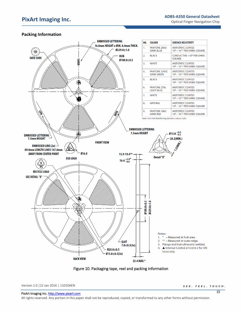
Packing Information
Figure 10. Packaging tape, reel and packing information
16
PixArt Imaging Inc. ADBS-A350 General Datasheet
Optical Finger Navigation Chip
ADBS-A350 General Datasheet Optical Finger Navigation Chip
PixArt Imaging Inc. http://www.pixart.com All rights reserved. Any portion in this paper shall not be reproduced, copied, or transformed to any other forms without permission.
Version 1.0 |22 Jan 2016 | 11010AEN
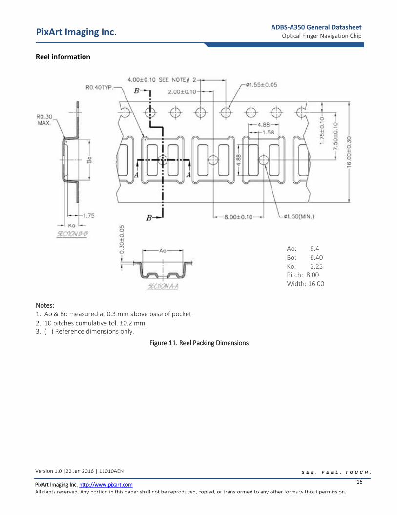
Reel information
Notes: 1. Ao & Bo measured at 0.3 mm above base of pocket.
2. 10 pitches cumulative tol. ±0.2 mm. 3. ( ) Reference dimensions only.
Figure 11. Reel Packing Dimensions
Ao: 6.4 Bo: 6.40 Ko: 2.25 Pitch: 8.00 Width: 16.00