acpi implementers guide - baldwinphoenix/reference/docs/acpi_impguide.pdf · acpi implementers’...
TRANSCRIPT
ACPI Implementers GuideIntel
Microsoft
ToshibaApril 4, 1997
ACPI Implementers’ Guide Draft 04/04/97
11:04 AM Intel/Microsoft/Toshiba1-2
Draft
Copyright © 1996, Intel Corporation, Microsoft Corporation, Toshiba Corp.All rights reserved.
INTELLECTUAL PROPERTY DISCLAIMER
THIS SPECIFICATION IS PROVIDED “AS IS” WITH NO WARRANTIES WHATSOEVER INCLUDING ANYWARRANTY OF MERCHANTABILITY, FITNESS FOR ANY PARTICULAR PURPOSE, OR ANYWARRANTY OTHERWISE ARISING OUT OF ANY PROPOSAL, SPECIFICATION, OR SAMPLE.
NO LICENSE, EXPRESS OR IMPLIED, BY ESTOPPEL OR OTHERWISE, TO ANY INTELLECTUALPROPERTY RIGHTS IS GRANTED OR INTENDED HEREBY.
INTEL, MICROSOFT, AND TOSHIBA, DISCLAIM ALL LIABILITY, INCLUDING LIABILITY FORINFRINGEMENT OF PROPRIETARY RIGHTS, RELATING TO IMPLEMENTATION OF INFORMATIONIN THIS SPECIFICATION. INTEL, MICROSOFT, AND TOSHIBA, DO NOT WARRANT OR REPRESENTTHAT SUCH IMPLEMENTATION(S) WILL NOT INFRINGE SUCH RIGHTS.
THIS DOCUMENT IS A DRAFT FOR COMMENT ONLY AND IS SUBJECT TO CHANGE WITHOUTNOTICE. READERS SHOULD NOT DESIGN PRODUCTS BASED ON THIS DOCUMENT.
Microsoft, Win32, Windows, and Windows NT are registered trademarks of Microsoft Corporation. I2C is a trademark of Phillips Semiconductors. All other product names are trademarks, registered trademarks, or servicemarks of their respective owners.
ACPI Implementers’ Guide Draft 04/04/97
11:04 AM Intel/Microsoft/Toshiba1-3
Revisions
The Draft Revision 0.4 of the ACPI Implementers’ Guide (dated March 19, 1997) was the first release of theGuide and is the baseline for all revisions documented in the following table.
Date posted onwww.teleport.com
Revisionnumber
Change Contributor
4/2/97 0.41 In section 3.4.1, “Main File ofDesktop Concept MachineSample Code,” in the PX43Device object code, deleted theOperationRegion named CFG3and added an instructivecomment to the OperationRegion named GPOB.
In section 3.4.2, “SuperIO ASLInclude File,” corrected theOffset term values. This samecorrection also had to be madeto section 3.3.4, “OperationRegion and Field Definitions fora Super I/O Chip.”
Randall Scott, Intel
4/2/97 0.41 Corrected ASL code examples tocorrectly use ASL specificationnaming convention that firstargument in argument listreceived by a called controlmethod is named Arg0, secondargument in list (if any) isnamed Arg1, and so on.
Mark Williams, Microsoft
ACPI Implementers’ Guide Draft 04/04/97
11:04 AM Intel/Microsoft/Toshiba1-4
Contents
1. INTRODUCTION.................................................................................................................................. 1-7
1.1 STRUCTURE OF THE ACPI IMPLEMENTERS’ GUIDE................................................................................ 1-71.2 DEFINITION OF TERMS ......................................................................................................................... 1-8
2. ACPI MOBILE CONCEPT MACHINE............................................................................................. 2-15
2.1 MOBILE CONCEPT MACHINE BLOCK DIAGRAM ................................................................................... 2-152.2 DEVICES USED ON THE MOBILE CONCEPT MACHINE ........................................................................... 2-172.3 DATA AND ADDRESS BUS STRUCTURE ................................................................................................ 2-17
2.3.1 Encoding the Data and Address Bus Structure in ASL ............................................................... 2-172.3.1.1 Filling in the Root PCI Bus Scope with Static Device Objects ..............................................................2-192.3.1.2 Filling in the ISA Scope with Static Device Objects .............................................................................2-212.3.1.3 Filling in the \_SB Scope with Static Device Objects............................................................................2-23
2.4 ADDING DYNAMIC EVENT HANDLING TO THE ACPI NAME SPACE ....................................................... 2-252.4.1 Use of an Embedded Controller on the Mobile Concept Machine .............................................. 2-25
2.4.1.1 Embedded Controller Operation Region and Fields ..............................................................................2-262.4.1.2 Handling Embedded Controller Lid Switch Events ...............................................................................2-28
2.4.2 Handling Device Swapping in the Bay ....................................................................................... 2-292.4.3 Handling Dock Events ............................................................................................................... 2-32
2.4.3.1 Handling Dock Events as General Purpose Events (GPEs)....................................................................2-322.4.3.2 ACPI Name Space Objects that Handle Dock Events ............................................................................2-332.4.3.3 Walking Through a Dock Event............................................................................................................2-35
2.4.4 Device Status Changes .............................................................................................................. 2-362.4.4.1 ACPI Name Space for the Joystick Device............................................................................................2-382.4.4.2 Sample ASL Code for the Joystick Device............................................................................................2-39
2.4.5 Device Resource Setting Changes.............................................................................................. 2-402.5 COMPLETE MOBILE CONCEPT MACHINE ACPI NAME SPACE ............................................................... 2-412.6 COMPLETE LISTING IF THE MOBILE CONCEPT MACHINE ASL CODE .................................................... 2-44
3. ACPI DESKTOP CONCEPT MACHINE .......................................................................................... 3-57
3.1 DESKTOP CONCEPT MACHINE DESIGN OVERVIEW............................................................................... 3-583.1.1 Hardware Devices ..................................................................................................................... 3-583.1.2 Desktop Block Diagram............................................................................................................. 3-59
3.2 DESKTOP CONCEPT MACHINE ACPI NAME SPACE .............................................................................. 3-593.2.1 Structure of the Data and Address Buses in ACPI Name Space.................................................. 3-603.2.2 All the Objects in the ACPI Name Space.................................................................................... 3-60
3.3 IMPLEMENTATION EXAMPLES FROM THE DESKTOP CONCEPT MACHINE................................................ 3-633.3.1 Power Resource Implementation................................................................................................ 3-633.3.2 Thermal Zone Implementation ................................................................................................... 3-64
3.3.2.1 Physical Components of Thermal Management.....................................................................................3-643.3.2.2 Defining a Thermal Policy for the Desktop Concept Machine ...............................................................3-653.3.2.3 Writing ASL Code that Carries Out the Thermal Policy........................................................................3-66
3.3.3 Power Button Support................................................................................................................ 3-733.3.3.1 Power Button Implementation on the Desktop Concept Machine ..........................................................3-733.3.3.2 Writing ASL Code that Supports the Desktop Power Button.................................................................3-73
3.3.4 Operation Region and Field Definitions for a Super I/O Chip ................................................... 3-743.4 DESKTOP SAMPLE ASL CODE ............................................................................................................ 3-75
3.4.1 Main File of Desktop Concept Machine Sample Code ............................................................... 3-763.4.2 Super IO ASL Include File......................................................................................................... 3-803.4.3 FDC ASL Include File ............................................................................................................... 3-813.4.4 UART1 ASL Include File ........................................................................................................... 3-833.4.5 UART2 ASL Include File ........................................................................................................... 3-863.4.6 Printer ASL Include File............................................................................................................ 3-91
ACPI Implementers’ Guide Draft 04/04/97
11:04 AM Intel/Microsoft/Toshiba1-5
3.4.7 PS2 Mouse and Keyboard Port Device ASL Include File ........................................................... 3-963.4.8 Include File ASL Code for the Single Configuration ISA Devices .............................................. 3-98
3.4.8.1 SMC Super I/O Device ASL Include File ...........................................................................................3-1013.4.8.2 Floppy Disk Controller ASL Include File............................................................................................3-102
4. ACPI SERVER CONCEPT MACHINE ............................................................................................4-105
4.1 OVERVIEW OF THE SERVER CONCEPT MACHINE DESIGN.....................................................................4-1054.2 SERVER BLOCK DIAGRAMS ...............................................................................................................4-107
4.2.1 Embedded Controller Details ...................................................................................................4-1084.2.2 Removable Drive Details ..........................................................................................................4-1094.2.3 Hot Swap Interface Details .......................................................................................................4-110
4.3 IMPLEMENTATION EXAMPLES FROM THE SERVER CONCEPT MACHINE.................................................4-1134.3.1 PCI Interrupt Routing...............................................................................................................4-1134.3.2 Managing Multiple Removable Hard Drives.............................................................................4-1144.3.3 Operation Region and Field Declarations for a Super I/O Chip................................................4-115
4.4 SERVER CONCEPT MACHINE SAMPLE ASL CODE ...............................................................................4-1174.5 SERVER CONCEPT MACHINE ACPI NAME SPACE ...............................................................................4-1184.6 SERVER SAMPLE ASL CODE .............................................................................................................4-121
4.6.1.1 National 307 Super I/O Chip Include File...........................................................................................4-1284.6.1.2 Super I/O Chip PS2 Port Include File .................................................................................................4-1314.6.1.3 Super I/O Chip Floppy Disk Controller Include File ...........................................................................4-1334.6.1.4 Super I/O Chip LPT Port Include File.................................................................................................4-1354.6.1.5 Super I/O Chip UART1 (UARA) Include File.....................................................................................4-1404.6.1.6 Super I/O Chip UART2 (UARTB) Include File ..................................................................................4-1444.6.1.7 Include File ASL Code for the Single Configuration ISA Devices .......................................................4-146
5. ACPI BIOS CASE STUDY.................................................................................................................5-151
5.1 TRAJAN ARCHITECTURE ...................................................................................................................5-1515.1.1 Modeling the Trajan Motherboard with Objects in the ACPI Namespace..................................5-1525.1.2 Trajan Interrupt Structure ........................................................................................................5-152
5.2 INITIALIZING THE ACPI BIOS DURING POST AND COLD BOOT SEQUENCE ........................................5-1565.2.1 Building the ACPI Tables in Memory .......................................................................................5-1575.2.2 Sizing Memory, Allocating Memory, Fixing Up Table Pointers, and Copying ACPI Tables intoMemory.............................................................................................................................................5-1575.2.3 Initializing the Chipset Registers ..............................................................................................5-1625.2.4 Saving the Chipset /Configuration Data ...................................................................................5-162
5.3 POWER MANAGEMENT USING ACPI ON THE TRAJAN MOTHERBOARD.................................................5-1635.3.1 Device Power Management ......................................................................................................5-1635.3.2 Processor Power Management..................................................................................................5-1645.3.3 System Power Management ......................................................................................................5-164
5.3.3.1 The BIOS’s Role in Transitioning Out of the Working State (S0) .......................................................5-1645.3.3.2 The BIOS’s Role in Waking from S1..................................................................................................5-1645.3.3.3 The BIOS’s Role in Waking from S2..................................................................................................5-1655.3.3.4 The BIOS’s Role in Waking from S3..................................................................................................5-1655.3.3.5 The BIOS’s Role in Waking from S4..................................................................................................5-166
5.4 PLUG AND PLAY USING ACPI ON THE TRAJAN MOTHERBOARD ..........................................................5-1665.4.1 Name Space Objects for Single-Configuration Devices.............................................................5-1665.4.2 Name Space Objects for Multiple-Configuration Devices .........................................................5-1675.4.3 Field Declarations....................................................................................................................5-1675.4.4 Example _CRS, _SRS, _STA, and _DIS Methods for the FDC...................................................5-167
5.5 DOCKING USING ACPI ON THE TRAJAN MOTHERBOARD ....................................................................5-1685.5.1 Field Declarations....................................................................................................................5-1695.5.2 Example _ADR, _UID, _EJ0, and Device Objects for the Dock ................................................5-1705.5.3 Example Synchronization and Notifications..............................................................................5-170
5.6 SWITCHING BETWEEN ACPI AND LEGACY MODES ON THE TRAJAN MOTHERBOARD............................5-170
ACPI Implementers’ Guide Draft 04/04/97
11:04 AM Intel/Microsoft/Toshiba1-6
5.6.1 Switching From Legacy to ACPI Mode .....................................................................................5-1715.6.2 Switching From ACPI to Legacy Mode .....................................................................................5-171
6. USING THE ACPI EMBEDDED CONTROLLER AND SMBUS INTERFACES..........................6-173
6.1 EMBEDDED CONTROLLER EXAMPLE #1 .............................................................................................6-1736.2 EMBEDDED CONTROLLER EXAMPLE #2 .............................................................................................6-176
7. APPENDIX - SUGGESTED VALIDATION AND TEST PROCEDURES.......................................7-183
7.1 STEP 1: STATIC CHECKING OF ACPI TABLES, NAMESPACE, AND INT 15H FUNCTIONS ........................7-1837.1.1 Double-checking for Specification Compliance ........................................................................7-1837.1.2 Getting the Common Mistakes Out of ACPI Tables, ACPI Name Space, and INT 15h Calls......7-1837.1.3 Using Specific Tools .................................................................................................................7-183
7.2 STEP 2: BOOTING WITH AN ACPI-COMPATIBLE OS............................................................................7-1847.2.1 Using Specific Tools .................................................................................................................7-184
7.3 STEP 3: EXERCISING ACPI FUNCTIONALITY ......................................................................................7-1847.3.1 Using Specific Tools .................................................................................................................7-184
7.4 STEP 4: EXERCISING OVERALL ACPI-COMPATIBLE OS FUNCTIONALITY ............................................7-1857.5 STEP 5: INSTALLING AND RUNNING ACPI-AWARE ADD-ON DEVICES .................................................7-185
8. APPENDIX - ACPI TIPS AND TRAPS .............................................................................................8-187
8.1 CONSTRUCTING THE ACPI TABLES ...................................................................................................8-1878.2 USING OBJECT NAMES IN THE ACPI NAME SPACE .............................................................................8-1878.3 USING THE ASL PROGRAMMING LANGUAGE......................................................................................8-1908.4 DECLARING POWERRESOURCE OBJECTS AND PROCESSOR OBJECTS.....................................................8-1908.5 COMPLETELY DEFINING THERMAL ZONES IN ASL CODE....................................................................8-1908.6 SPECIFYING PLUG AND PLAY DEVICE IDS AND CONFIGURATION DESCRIPTORS....................................8-1918.7 MAPPING THE ACPI TABLES INTO MEMORY......................................................................................8-1918.8 IMPLEMENTING THE SYSTEM WAKE FUNCTIONALITY .........................................................................8-192
ACPI Implementers’ Guide Draft 04/04/97
11:04 AM Intel/Microsoft/Toshiba1-7
1. Introduction
Note: This is the March 28, 1997, version of the ACPI Implementers’ Guide; the latest version of the Guide isalways available at www.teleport.com/~acpi.
The ACPI Implementers’ Guide is a practical guide for engineers that are working to get an ACPI-compatiblesystem design up and running. This Guide is designed to work with the ACPI Specification, Version 1.0, andthe ACPI Specification, Version 1.0, Errata publications; you need those other two publications nearby toeffectively use this Guide.
1.1 Structure of the ACPI Implementers’ Guide
This Guide has the following sections:
Section Number Title Description Suggested Use
2 - ACPI Mobile Concept Machine Describes a hypothetical mobileplatform design with a hardwareblock diagram, models thehardware with objects in ACPIname space, and fills the objectswith ASL code. Focuses on
• Using an embedded controller.
• Managing removable devicescoming and going in a bay.
• Managing docking andundocking events.
If you are designing and building amobile platform that has an ACPI-compatible chipset, use thischapter to get ideas for your designand to get blocks of sample ASLcode you can modify instead ofwriting all your ASL code fromscratch.
3 - ACPI Desktop ConceptMachine
Describes a hypothetical desktopplatform design with a hardwareblock diagram, models thehardware with objects in ACPIname space, and fills the objectswith ASL code. Focuses on
• PowerResourceimplementation.
• Thermal Zoneimplementation.
• Power Button implementation.
If you are designing and building aDesktop that has an ACPI-compatible chipset, use thischapter to get ideas for your designand to get blocks of sample ASLcode you can modify instead ofwriting all your ASL code fromscratch.
4 - ACPI Server Concept Machine Describes a hypothetical serverplatform design with a hardwareblock diagram, models thehardware with objects in ACPIname space, and fills the objectswith ASL code. Focuses on
• Managing removable diskdrives.
If you are designing and building aServer that has an ACPI-compatible chipset, use thischapter to get ideas for your designand to get blocks of sample ASLcode you can modify instead ofwriting all your ASL code fromscratch.
5 - ACPI BIOS Case Study for theTrajan 430TX Motherboard
This section goes one step beyondthe concept machine sections. This
Use this chapter both to double-check the validity of your ASL
ACPI Implementers’ Guide Draft 04/04/97
11:04 AM Intel/Microsoft/Toshiba1-8
Section Number Title Description Suggested Use
section uses the ACPI-compatibleTrajan 430TX motherboard as acase study and shows how to buildan ACPI BIOS for an actual ACPI-compatible motherboard product.
code and to package your ACPIBIOS.
6 - Using the ACPI EmbeddedController and SMBus Interfaces
Presents sample ACPI EmbeddedController Interface and ACPISMBus interface implementationsand walks through the transactionprotocol across these buses foreach of these implementations.
Use to better understand these twoACPI interfaces.
7 - Appendix: Hands-On GettingStarted
Walks through a four-stepprocedure that can be used to testthe integration of your ACPIhardware and firmware with anACPI-compatible OS.
When you have your ACPI-compatible prototype built, use thesuggested test procedure as astarting point in developing yourown in-house test procedure.
8 - Appendix: Tips and Traps Lists errors commonly made byACPI implementers and gives tipsfor avoiding these errors.
Use as a checklist while buildingprototype ACPI-compatiblehardware, writing ASL code, andpackaging your ACPI BIOS; thisenables you to avoid commonerrors.
1.2 Definition of Terms
This section contains term definitions from the ACPI Specification, Revision 1.0, that are particularly relevantto this Guide.
ACPI Name Space:
The ACPI Name Space is a hierarchical tree structure in OS-controlled memory that contains namedobjects. These objects may be data objects, control method objects, bus/device package objects, etc. The OSdynamically changes the contents of the Name Space at run time by loading and/or unloading definitionblocks from the ACPI Tables that reside in the ACPI BIOS. All the information in the ACPI Name Spacecomes from the Differentiated System Description Table, which contains the Differentiated DefinitionBlock, and one or more other definition blocks.
AML:
ACPI control method Machine Language. Pseudocode for a virtual machine supported by an ACPI-compatible operating system and in which ACPI control methods are written.
ASL:
ACPI control method Source Language. The programming language equivalent for AML. ASL iscompiled into AML images.
C0 Processor Power State:
While the processor is in this state, it executes instructions.
C1 Processor Power State
ACPI Implementers’ Guide Draft 04/04/97
11:04 AM Intel/Microsoft/Toshiba1-9
This processor power state has the lowest latency, The hardware latency on this state is required to be lowenough that the operating software does not consider the latency aspect of the state when deciding whetherto use it. Aside from putting the processor in a non-executing power state, this state has no other software-visible effects.
C2 Processor Power State:
The C2 state offers improved power savings over the C1 state. The worst-case hardware latency for thisstate is declared in the FACP Table and the operating software can use this information to determinewhen the C1 state should be used instead of the C2 state. Aside from putting the processor in a non-executing power state, this state has no other software-visible effects.
C3 Processor Power State:
The C3 state offers improved power savings of the C1 and C2 states. The worst-case hardware latency forthis state is declared in the FACP Table, and the operating software can use this information to determinewhen the C2 state should be used instead of the C3 state. While in the C3 state, the processor’s cachesmaintain state but ignore any snoops. The operating software is responsible for ensuring that the cachesmaintain coherency.
Control Method:
A control method is a definition of how the OS can perform a simple hardware task. For example, the OSinvokes control methods to read the temperature of a thermal zone. Control methods are written in anencoded language called AML that can be interpreted and executed by the ACPI-compatible OS. AnACPI-compatible system must provide a minimal set of control methods in the ACPI tables. The OSprovides a set of well-defined control methods that ACPI table developers can reference in their controlmethods. OEMs can support different revisions of chip sets with one BIOS by either including controlmethods in the BIOS that test configurations and respond as needed or by including a different set ofcontrol methods for each chip set revision.
CPU, or processor:
The central processor unit (CPU), or processor, is the part of a platform that executes the instructions thatdo the work. An ACPI-compatible OS can balance processor performance against power consumption andthermal states by manipulating the processor clock speed and cooling controls. The ACPI specificationdefines a working state, labeled G0, in which the processor executes instructions. Processor low powerstates, labeled C1 through C3, are also defined. In the low power states the processor executes noinstructions, thus reducing power consumption and, potentially, operating temperatures.
D0 - Fully-On:
This device power state is assumed to be the highest level of power consumption. The device is completelyactive and responsive, and is expected to remember all relevant context continuously.
D1:
The meaning of the D1 device power state is defined by each class of device; it may not be defined bymany classes of devices. In general, D1 is expected to save less power and preserve more device contextthan D2.
D2:
The meaning of the D2 device power state is defined by each class of device; it may not be defined bymany classes of devices. In general, D2 is expected to save more power and preserve less device contextthan D1 or D0. Buses in D2 may cause the device to loose some context (i.e., by reducing power on thebus, thus forcing the device to turn off some of its functions).
ACPI Implementers’ Guide Draft 04/04/97
11:04 AM Intel/Microsoft/Toshiba1-10
D3 - Off:
Power has been fully removed from the device. The device context is lost when this state is entered, so theOS software will reinitialize the device when powering it back on. Since device context and power arelost, devices in this state do not decode their addresses lines. Devices in this state have the longest restoretimes. All classes of devices define this state.
Definition Block:
A definition block contains information about hardware implementation and configuration details in theform of data and control methods, encoded in AML. An OEM can provide one or more definition blocksin the ACPI Tables. One definition block must be provided: the Differentiated Definition Block, whichdescribes the base system. Upon loading the Differentiated Definition Block, the OS inserts the contents ofthe Differentiated Definition Block into the ACPI Name Space. Other definition blocks, which the OS candynamically insert and remove from the active ACPI Name Space, can contain references to theDifferentiated Definition Block.
Device:
Hardware components outside the core chip set of a platform. Examples of devices are LCD panels, videoadapters, IDE CD-ROM and hard disk controllers, COM ports, etc. In the ACPI scheme of powermanagement, buses are devices.
Differentiated System Description Table:
An OEM must supply a Differentiated System Description Table (DSDT) to an ACPI-compatible OS. TheDSDT contains the Differentiated Definition Block, which supplies the implementation and configurationinformation about the base system. The OS always inserts the DSDT information into the ACPI NameSpace at system boot time, and never removes it.
Embedded Controller and Embedded Controller Interface:
Embedded controllers are the general class of microcontrollers used to support OEM-specificimplementations, mainly in mobile environments. The ACPI specification supports embedded controllersin any platform design, as long as the microcontroller conforms to one of the models described in thissection. The embedded controller performs complex low-level functions, through a simple interface to thehost microprocessor(s). ACPI defines a standard hardware and software communications interfacebetween an OS driver and an embedded controller; this is the embedded controller interface. Thisinterface allows any OS to provide a standard driver that can directly communicate with an embeddedcontroller in the system, thus allowing other drivers within the system to communicate with and use theresources of system embedded controllers (for example, Smart Battery and AML code). This in turnenables the OEM to provide platform features that the OS and applications can use.
Firmware ACPI Control Structure:
The Firmware ACPI Control Structure (FACS) is a structure in read/write memory that the BIOS uses forhandshaking between the firmware and the OS, and is passed to an ACPI-compatible OS via the FixedACPI Description Table (FACP). The FACS contains the system’s hardware signature at last boot, thefirmware waking vector, and the global lock.
Fixed ACPI Description Table:
An OEM must provide a Fixed ACPI Description Table (FACP) to an ACPI-compatible OS in the RootSystem Description Table. The FACP contains the ACPI Hardware Register Block implementation andconfiguration details the OS needs to direct management of the ACPI Hardware Register Blocks, as wellas the physical address of the Differentiated System Description Table (DSDT) that contains otherplatform implementation and configuration details. The OS always inserts the name space informationdefined in the Differentiated Definition Block in the DSDT into the ACPI Name Space at system boottime, and the OS never removes it.
ACPI Implementers’ Guide Draft 04/04/97
11:04 AM Intel/Microsoft/Toshiba1-11
Fixed Platform Features, Fixed Feature Registers, and Fixed Feature Events
Fixed platform features are a set of features offered by an ACPI interface. The ACPI specification placesrestrictions on where and how the hardware programming model is generated. All fixed features, if used,are implemented as described in this specification so that the ACPI driver can directly access the fixedfeature registers. The fixed feature registers are a set of hardware registers in fixed feature register spaceat specific address locations in system IO address space. ACPI defines register blocks for fixed features(each register block gets a separate pointer from the FACP ACPI table). Fixed feature events are a set ofevents that occur at the ACPI interface when a paired set of status and event bits in the fixed featureregisters are set at the same time. While a fixed feature event occurs an SCI is raised. For ACPI fixed-feature events, the ACPI driver (or an ACPI-aware driver) acts as the event handler.
G0 - Working:
A computer state where the system dispatches user mode (application) threads and they execute. In thisstate, devices (peripherals) are dynamically having their power state changed. The user will be able toselect (through some user interface) various performance/power characteristics of the system to have thesoftware optimize for performance or battery life. The system responds to external events in real time. It isnot safe to disassemble the machine in this state.
G1 - Sleeping:
A computer state where the computer consumes a small amount of power, user mode threads are not beingexecuted, and the system “appears” to be off (from an end user’s perspective, the display is off, etc.).Latency for returning to the Working state varies on the wakeup environment selected prior to entry ofthis state (for example, should the system answer phone calls, etc.). Work can be resumed withoutrebooting the OS because large elements of system context are saved by the hardware and the rest bysystem software. It is not safe to disassemble the machine in this state.
G2/S5 - Soft Off:
A computer state where the computer consumes a minimal amount of power. No user mode or systemmode code is run. This state requires a large latency in order to return to the Working state. The system’scontext will not be preserved by the hardware. The system must be restarted to return to the Workingstate. It is not safe to disassemble the machine.
G3 - Mechanical Off:
A computer state that is entered and left by a mechanical means (e.g. turning off the system’s powerthrough the movement of a large red switch). This operating mode is required by various governmentagencies and countries. It is implied by the entry of this off state through a mechanical means that the noelectrical current is running through the circuitry and it can be worked on without damaging the hardwareor endangering the service personnel. The OS must be restarted to return to the Working state. Nohardware context is retained. Except for the real time clock, power consumption is zero.
Generic Platform Features and General Purpose Event (GPE) Registers:
A generic feature of a platform is value-added hardware implemented through control methods andgeneral-purpose events. The general purpose event (GPE) registers contain the event programming modelfor generic features. All generic events generate SCIs.
Global System States:
Global system states apply to the entire system, and are visible to the user. The various global systemstates are labeled G0 through G3 in the ACPI specification.
Legacy State, Legacy Hardware, and Legacy OS:
ACPI Implementers’ Guide Draft 04/04/97
11:04 AM Intel/Microsoft/Toshiba1-12
Legacy state is a computer state where power management policy decisions are made by the platformhardware/firmware shipped with the system. The legacy power management features found in today’ssystems are used to support power management in a system that uses a legacy OS that does not support theOS-directed power management architecture. Legacy hardware is a computer system that has no ACPI orOSPM power management support. A legacy OS is an operating system that is not aware of and does notdirect power management functions of the system. Included in this category are operating systems withAPM 1.x support.
Multiple APIC Description Table:
The Multiple APIC Description Table (APIC) is used on systems supporting the APIC to describes theAPIC implementation. Following the Multiple APIC Description Table is a list of APIC structures thatdeclare the APIC features of the machine.
Object:
The nodes of the ACPI Name Space are objects inserted in the tree by the OS using the information in thesystem definition tables. These objects can be data objects, package objects, control method objects, etc.Package objects refer to other objects. Objects also have type, size, and relative name.
Object name:
Object names are part of the ACPI Name Space. There is a set of rules for naming objects.
Package:
A set of objects.
Persistent System Description Table:
Persistent System Description Tables are Definition Blocks, similar to Secondary System DescriptionTables, except a Persistent System Description Table can be saved by the OS and automatically loaded atevery boot.
Power Button:
A user push button that switches the system from the sleeping/soft off state to the working state, andsignals the OS to transition to a sleeping/soft off state from the working state.
Power Resources:
Power resources are resources (for example, power planes and clock sources) that a device requires tooperate in a given power state.
Power Sources:
The battery and AC adapter that supply power to a platform.
Root System Description Pointer:
An ACPI compatible system must provide a Root System Description Pointer in the systems low addressspace. This structure’s only purpose is to provide the physical address of the Root System DescriptionTable.
Root System Description Table:
The Root System Description Table starts with the signature ‘RSDT,’ followed by an array of physicalpointers to the other System Description Tables that provide various information on other standards thatare defined on the current system. The OS locates that Root System Description Table by following thepointer in the Root System Description Pointer structure.
ACPI Implementers’ Guide Draft 04/04/97
11:04 AM Intel/Microsoft/Toshiba1-13
S1 Sleeping State:
The S1 sleeping state is a low wake-up latency sleeping state. In this state, no system context is lost (CPUor chip set) and hardware maintains all system context.
S2 Sleeping State
The S2 sleeping state is a low wake-up latency sleeping state. This state is similar to the S1 sleeping stateexcept the CPU and system cache context is lost (the OS is responsible for maintaining the caches andCPU context). Control starts from the processor’s reset vector after the wake-up event.
S3 Sleeping State:
The S3 sleeping state is a low wake-up latency sleeping state where all system context is lost exceptsystem memory. CPU, cache, and chip set context are lost in this state. Hardware maintains memorycontext and restores some CPU and L2 configuration context. Control starts from the processor’s resetvector after the wake-up event.
S4 Sleeping State:
The S4 sleeping state is the lowest power, longest wake-up latency sleeping state supported by ACPI. Inorder to reduce power to a minimum, it is assumed that the hardware platform has powered off all devices.Platform context is maintained.
S4 - Non-Volatile Sleep:
S4 Non-Volatile Sleep (NVS) is a special global system state that allows system context to be saved andrestored (relatively slowly) when power is lost to the motherboard. If the system has been commanded toenter S4, the OS will write all system context to a non-volatile storage file and leave appropriate contextmarkers. The machine will then enter the S4 state. When the system leaves the Soft Off or Mechanical Offstate, transitioning to Working (G0) and restarting the OS, a restore from a NVS file can occur. This willonly happen if a valid NVS data set is found, certain aspects of the configuration of the machine has notchanged, and the user has not manually aborted the restore. If all these conditions are met, as part of theOS restarting it will reload the system context and activate it. The net effect for the user is what looks likea resume from a Sleeping (G1) state (albeit slower). The aspects of the machine configuration that mustnot change include, but are not limited to, disk layout and memory size. It might be possible for the userto swap a PC Card or a Device Bay device, however.
Note that for the machine to transition directly from the Soft Off or Sleeping states to S4, the systemcontext must be written to non-volatile storage by the hardware; entering the Working state first so the OSor BIOS can save the system context takes too long from the user’s point of view. The transition fromMechanical Off to S4 is likely to be done when the user is not there to see it.
Because the S4 state relies only on non-volatile storage, a machine can save its system context for anarbitrary period of time (on the order of many years).
S5 Soft Off State:
The S5 state is similar to the S4 state except the OS does not save any context nor enable any devices towake the system. The system is in the “soft” off state and requires a complete boot when awakened.Software uses a different state value to distinguish between the S5 state and the S4 state to allow for initialboot operations within the BIOS to distinguish whether or not the boot is going to wake from a savedmemory image.
Secondary System Description Table:
Secondary System Description Tables are a continuation of the Differentiated System Description Table.Multiple Secondary System Description Tables can be used as part of a platform description. After the
ACPI Implementers’ Guide Draft 04/04/97
11:04 AM Intel/Microsoft/Toshiba1-14
Differentiated System Description Table is loaded into ACPI name space, each secondary description tablewith a unique OEM Table ID is loaded. This allows the OEM to provide the base support in one table,while adding smaller system options in other tables. Note: Additional tables can only add data, theycannot overwrite data from previous tables.
Sleep Button:
A user push button that switches the system from a sleeping state to the working state, and signals the OSto transition to a sleeping state from the working state.
Smart Battery Subsystem and Smart Battery Table:
A battery subsystem that conforms to the following specifications: --battery, charger, selector list—and theadditional ACPI requirements. The Smart Battery table is an ACPI table used on platforms that have aSmart Battery Subsystem. This table indicates the energy levels trip points that the platform requires forplacing the system into different sleeping states and suggested energy levels for warning the user totransition the platform into a sleeping state.
SMBus and SMBus Interface:
SMBus is a two-wire interface based upon the I²C protocol. The SMBus is a low-speed bus that providespositive addressing for devices, as well as bus arbitration. ACPI defines a standard hardware and softwarecommunications interface between an OS bus driver and an SMBus Controller via an embeddedcontroller; this is the SMBus interface.
System Control Interrupt (SCI):
A system interrupt used by hardware to notify the OS of ACPI events. The SCI is a active low, shareable,level interrupt.
System Management Interrupt (SMI):
An OS-transparent interrupt generated by interrupt events on legacy systems. By contrast, on ACPIsystems, interrupt events generate an OS-visible interrupt that is shareable (edge-style interrupts will notwork). Hardware platforms that want to support both legacy operating systems and ACPI systems mustsupport a way of re-mapping the interrupt events between SMIs and SCIs when switching between ACPIand legacy models.
Thermal States:
Thermal states represent different operating environment temperatures within thermal zones of a system.A system can have one or more thermal zones; each thermal zone is the volume of space around aparticular temperature sensing device. The transitions from one thermal state to another are marked bytrip points, which are implemented to generate a System Control Interrupt (SCI) when the temperature ina thermal zone moves above or below the trip point temperature.
ACPI Implementers’ Guide Draft 04/04/97
11:04 AM Intel/Microsoft/Toshiba2-15
2. ACPI Mobile Concept Machine
This section describes a conceptual ACPI mobile personal computer. The primary differences a typical desktopsystem are that this mobile concept machine:
• Has an embedded controller that monitors the CPU temperature every few degrees.
• Has swappable drive bays.
• Uses a battery for a power source.
The mobile concept machine docking station has PCI slots plus a port for a joystick.
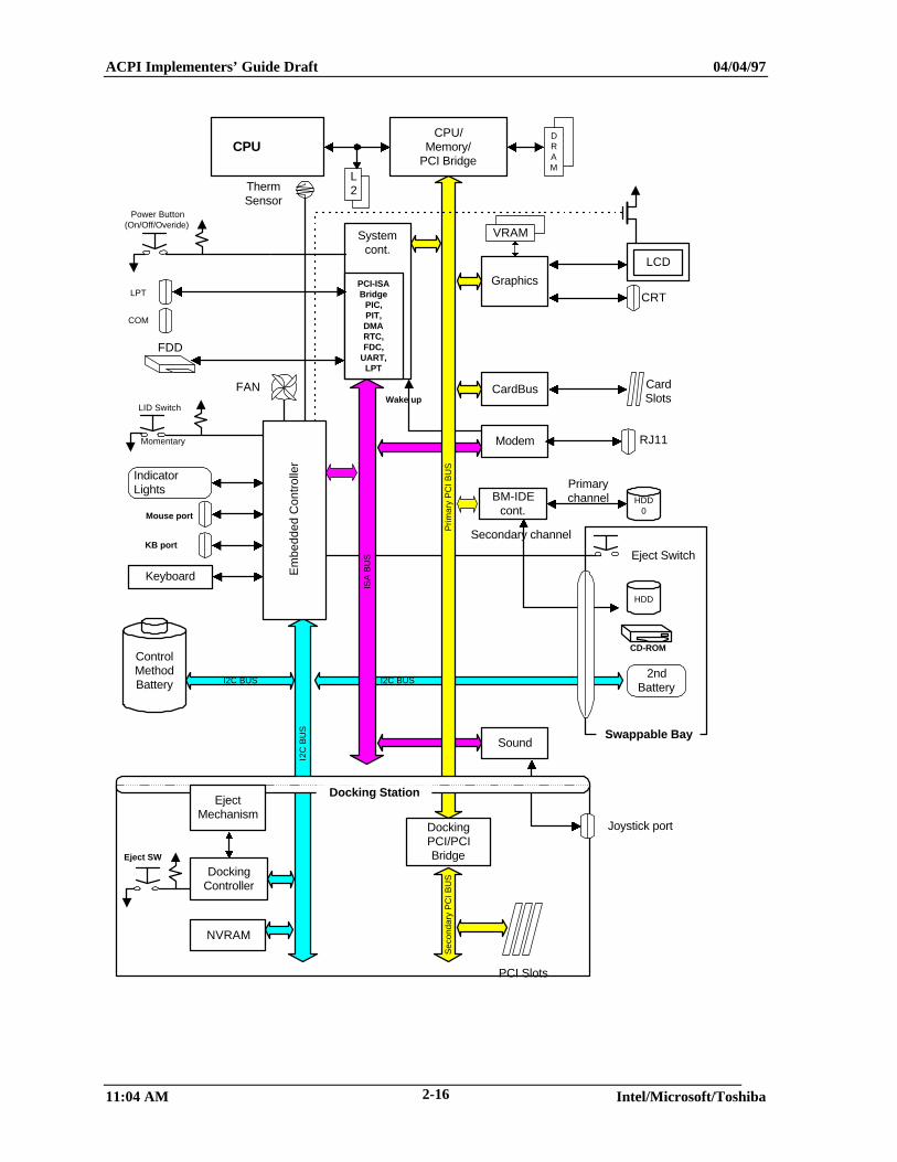
2.1 Mobile Concept Machine Block Diagram
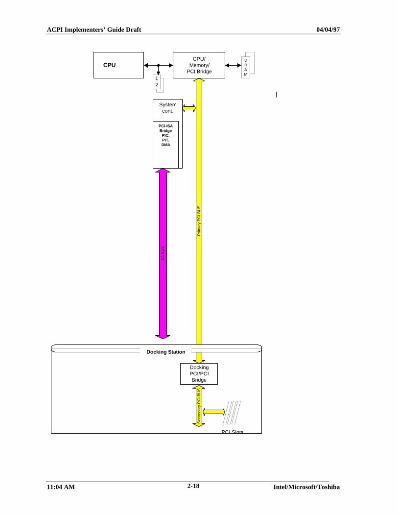
Figure 2-1 is a block diagram of the concept mobile platform. A prominent component of the mobile platformblock diagram is the embedded controller (in the upper-left part of Figure 2-1).
ACPI Implementers’ Guide Draft 04/04/97
11:04 AM Intel/Microsoft/Toshiba2-16
I2C BUS2nd
Battery
CPUCPU/
Memory/PCI Bridge
DRAM
Sound
Graphics
CardBus
Modem
L2
Prim
ary
PC
I BU
S
ISA
BU
S
I2C
BU
S
I2C BUS
VRAM
Swappable Bay
CRT
RJ11
CardSlots
FAN
DockingController
DockingPCI/PCIBridge
BM-IDEcont.
Sec
onda
ry P
CI B
US
PCI Slots
CD-ROM
FDD
HDD
NVRAM
Eject SW
Joystick port
HDD0
Systemcont.
Em
bedd
ed C
ontr
olle
r
Keyboard
IndicatorLights
KB port
Mouse port
Momentary
Power Button(On/Off/Overide)
EjectMechanism
LID Switch
ThermSensor
ControlMethodBattery
LCD
PCI-ISABridge
PIC,PIT,DMARTC,FDC,
UART,LPT
COM
LPT
Docking Station
Primarychannel
Secondary channel
Eject Switch
Wake up
ACPI Implementers’ Guide Draft 04/04/97
11:04 AM Intel/Microsoft/Toshiba2-17
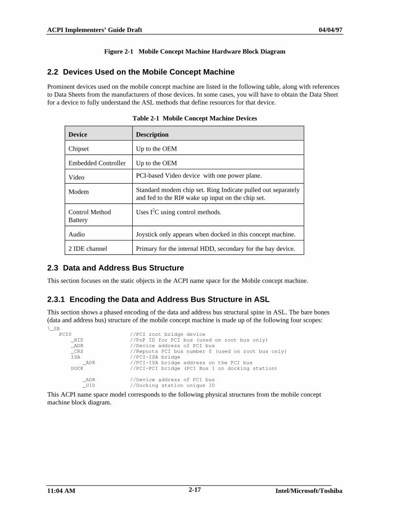
Figure 2-1 Mobile Concept Machine Hardware Block Diagram
2.2 Devices Used on the Mobile Concept Machine
Prominent devices used on the mobile concept machine are listed in the following table, along with referencesto Data Sheets from the manufacturers of those devices. In some cases, you will have to obtain the Data Sheetfor a device to fully understand the ASL methods that define resources for that device.
Table 2-1 Mobile Concept Machine Devices
Device Description
Chipset Up to the OEM
Embedded Controller Up to the OEM
Video PCI-based Video device with one power plane.
Modem Standard modem chip set. Ring Indicate pulled out separatelyand fed to the RI# wake up input on the chip set.
Control MethodBattery
Uses I2C using control methods.
Audio Joystick only appears when docked in this concept machine.
2 IDE channel Primary for the internal HDD, secondary for the bay device.
2.3 Data and Address Bus Structure
This section focuses on the static objects in the ACPI name space for the Mobile concept machine.
2.3.1 Encoding the Data and Address Bus Structure in ASL
This section shows a phased encoding of the data and address bus structural spine in ASL. The bare bones(data and address bus) structure of the mobile concept machine is made up of the following four scopes:\_SB
PCI0 //PCI root bridge device_HID //PnP ID for PCI bus (used on root bus only)_ADR //Device address of PCI bus_CRS //Reports PCI bus number 0 (used on root bus only)ISA //PCI-ISA bridge
_ADR //PCI-ISA bridge address on the PCI busDOCK //PCI-PCI bridge (PCI Bus 1 on docking station)
_ADR //Device address of PCI bus_UID //Docking station unique ID
This ACPI name space model corresponds to the following physical structures from the mobile conceptmachine block diagram.
ACPI Implementers’ Guide Draft 04/04/97
11:04 AM Intel/Microsoft/Toshiba2-18
CPUCPU/
Memory/PCI Bridge
DRAM
L2
Prim
ary
PC
I BU
S
ISA
BU
S
DockingPCI/PCIBridge
Sec
onda
ry P
CI B
US
PCI Slots
Systemcont.
PCI-ISABridge
PIC,PIT,DMA
Docking Station
ACPI Implementers’ Guide Draft 04/04/97
11:04 AM Intel/Microsoft/Toshiba2-19
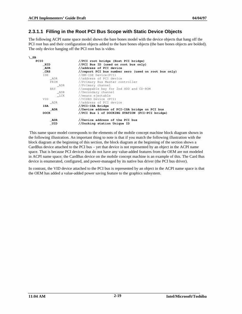
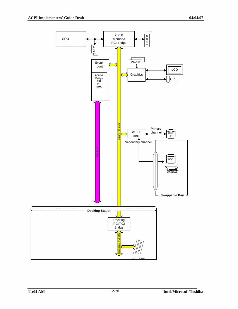
2.3.1.1 Filling in the Root PCI Bus Scope with Static Device Objects
The following ACPI name space model shows the bare bones model with the device objects that hang off thePCI root bus and their configuration objects added to the bare bones objects (the bare bones objects are bolded).The only device hanging off the PCI root bus is video.
\_SBPCI0 //PCI root bridge (Host PCI bridge)
_HID //PCI Bus ID (used on root bus only)_ADR //address of PCI device_CRS //report PCI bus number zero (used on root bus only)IDE //BM-IDE Device(PCI)
_ADR //address of PCI devicePRIM //Primary Bus Master controller
_ADR //Primary channelBAY //swappable bay for 2nd HDD and CD-ROM
_ADR //Secondary channel_LCK //means ejectable
VID //VIDEO Device (PCI)_ADR //address of PCI device
ISA //PCI-ISA Bridge_ADR //Device address of PCI-ISA bridge on PCI bus
DOCK //PCI Bus 1 of DOCKING STATION (PCI-PCI bridge)
_ADR //Device address of the PCI bus_UID //Docking station Unique ID
This name space model corresponds to the elements of the mobile concept machine block diagram shown inthe following illustration. An important thing to note is that if you match the following illustration with theblock diagram at the beginning of this section, the block diagram at the beginning of the section shows aCardBus device attached to the PCI bus – yet that device is not represented by an object in the ACPI namespace. That is because PCI devices that do not have any value-added features from the OEM are not modeledin ACPI name space; the CardBus device on the mobile concept machine is an example of this. The Card Busdevice is enumerated, configured, and power-managed by its native bus driver (the PCI bus driver).
In contrast, the VID device attached to the PCI bus is represented by an object in the ACPI name space is thatthe OEM has added a value-added power saving feature to the graphics subsystem.
ACPI Implementers’ Guide Draft 04/04/97
11:04 AM Intel/Microsoft/Toshiba2-20
CPUCPU/
Memory/PCI Bridge
DRAM
Graphics
L2
Prim
ary
PC
I BU
S
ISA
BU
S
VRAM
Swappable Bay
CRT
DockingPCI/PCIBridge
BM-IDEcont.
Sec
onda
ry P
CI B
US
PCI Slots
CD-ROM
HDD
HDD0
Systemcont.
LCD
PCI-ISABridge
PIC,PIT,DMA
Docking Station
Primarychannel
Secondary channel
ACPI Implementers’ Guide Draft 04/04/97
11:04 AM Intel/Microsoft/Toshiba2-21
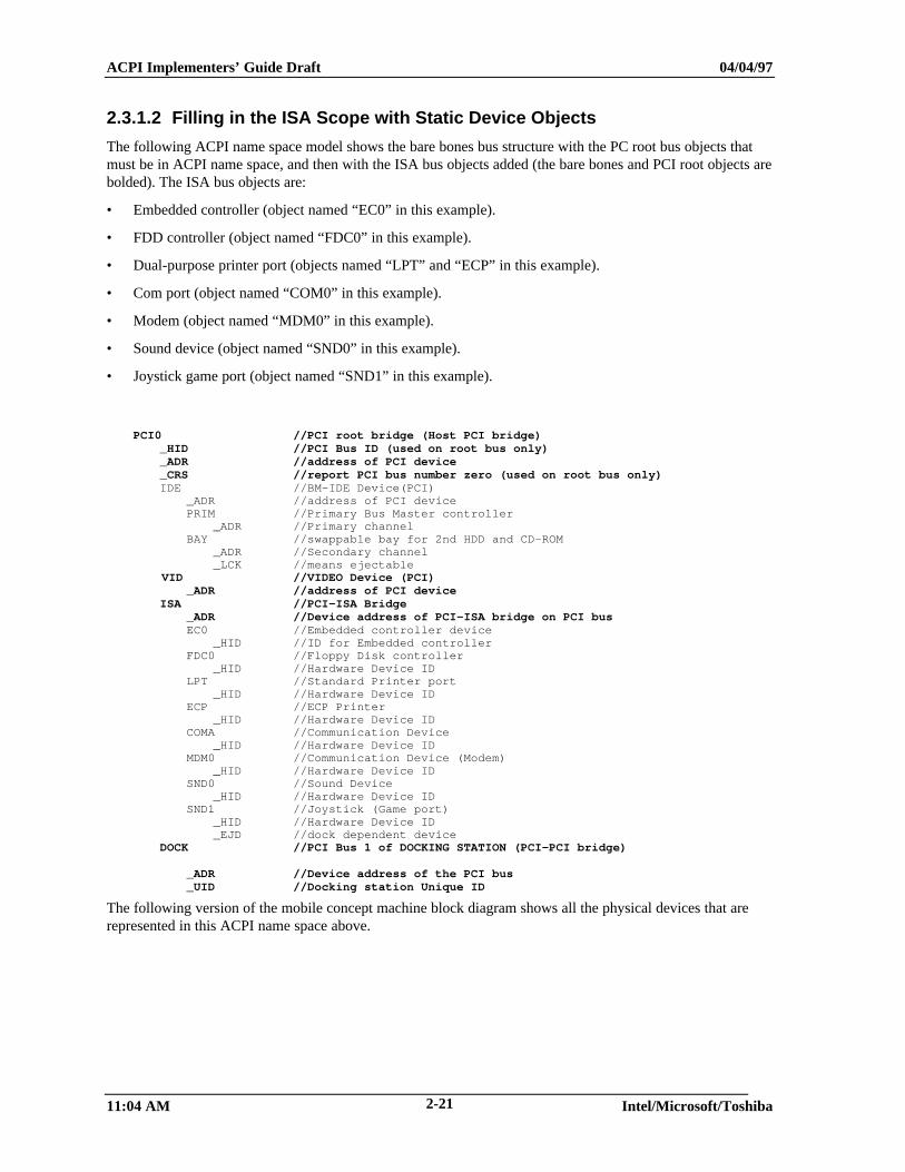
2.3.1.2 Filling in the ISA Scope with Static Device Objects
The following ACPI name space model shows the bare bones bus structure with the PC root bus objects thatmust be in ACPI name space, and then with the ISA bus objects added (the bare bones and PCI root objects arebolded). The ISA bus objects are:
• Embedded controller (object named “EC0” in this example).
• FDD controller (object named “FDC0” in this example).
• Dual-purpose printer port (objects named “LPT” and “ECP” in this example).
• Com port (object named “COM0” in this example).
• Modem (object named “MDM0” in this example).
• Sound device (object named “SND0” in this example).
• Joystick game port (object named “SND1” in this example).
PCI0 //PCI root bridge (Host PCI bridge)_HID //PCI Bus ID (used on root bus only)_ADR //address of PCI device_CRS //report PCI bus number zero (used on root bus only)IDE //BM-IDE Device(PCI)
_ADR //address of PCI devicePRIM //Primary Bus Master controller
_ADR //Primary channelBAY //swappable bay for 2nd HDD and CD-ROM
_ADR //Secondary channel_LCK //means ejectable
VID //VIDEO Device (PCI)_ADR //address of PCI device
ISA //PCI-ISA Bridge_ADR //Device address of PCI-ISA bridge on PCI busEC0 //Embedded controller device
_HID //ID for Embedded controllerFDC0 //Floppy Disk controller
_HID //Hardware Device IDLPT //Standard Printer port
_HID //Hardware Device IDECP //ECP Printer
_HID //Hardware Device IDCOMA //Communication Device
_HID //Hardware Device IDMDM0 //Communication Device (Modem)
_HID //Hardware Device IDSND0 //Sound Device
_HID //Hardware Device IDSND1 //Joystick (Game port)
_HID //Hardware Device ID_EJD //dock dependent device
DOCK //PCI Bus 1 of DOCKING STATION (PCI-PCI bridge)
_ADR //Device address of the PCI bus_UID //Docking station Unique ID
The following version of the mobile concept machine block diagram shows all the physical devices that arerepresented in this ACPI name space above.
ACPI Implementers’ Guide Draft 04/04/97
11:04 AM Intel/Microsoft/Toshiba2-22
CPUCPU/
Memory/PCI Bridge
DRAM
Sound
Graphics
Modem
L2
Prim
ary
PC
I BU
S
ISA
BU
S
VRAM
Swappable Bay
CRT
RJ11
DockingPCI/PCIBridge
BM-IDEcont.
Sec
onda
ry P
CI B
US
PCI Slots
CD-ROM
FDD
HDD
Joystick port
HDD0
Systemcont.
Em
bedd
ed C
ontr
olle
r
Keyboard
KB port
Mouse port
LCD
PCI-ISABridge
PIC,PIT,DMARTC,FDC,
UART,LPT
COM
LPT
Docking Station
Primarychannel
Secondary channel
Wake up
ACPI Implementers’ Guide Draft 04/04/97
11:04 AM Intel/Microsoft/Toshiba2-23
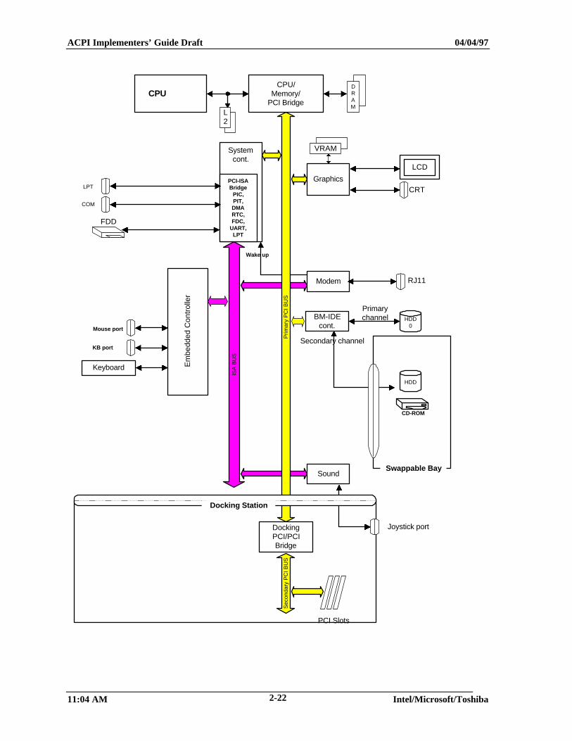
2.3.1.3 Filling in the \_SB Scope with Static Device Objects
The following ACPI name space model shows the bare bones model with the system bus (\_SB) objects added.The system bus objects are:
• Lid switch (named “LID” in this example)
• AC adapter (named “AC” in this example)
• Battery (named “BAT0” in this example)
\_SBLID //LID
_HID //LID IDBAT0 //Battery
_HID //Battery Device IDAC //AC AdapterPCI0 //PCI root bridge (Host PCI bridge)
_HID //PCI Bus ID (used on root bus only)_ADR //address of PCI device_CRS //report PCI bus number zero (used on root bus only)IDE //BM-IDE Device(PCI)
_ADR //address of PCI devicePRIM //Primary Bus Master controller
_ADR //Primary channelBAY //swappable bay for 2nd HDD and CD-ROM
_ADR //Secondary channel_LCK //means ejectable
VID //VIDEO Device (PCI)_ADR //address of PCI device
ISA //PCI-ISA Bridge_ADR //Device address of PCI-ISA bridge on PCI busEC0 //Embedded controller device
_HID //ID for Embedded controllerFDC0 //Floppy Disk controller
_HID //Hardware Device IDLPT //Standard Printer port
_HID //Hardware Device IDECP //ECP Printer
_HID //Hardware Device IDCOMA //Communication Device
_HID //Hardware Device IDMDM0 //Communication Device (Modem)
_HID //Hardware Device IDSND0 //Sound Device
_HID //Hardware Device IDSND1 //Joystick (Game port)
_HID //Hardware Device ID_EJD //dock dependent device
DOCK //PCI Bus 1 of DOCKING STATION (PCI-PCI bridge)
_ADR //Device address of the PCI bus_UID //Docking station Unique ID
This name space corresponds to the following parts of the mobile concept machine block diagram.
ACPI Implementers’ Guide Draft 04/04/97
11:04 AM Intel/Microsoft/Toshiba2-24
CPUCPU/
Memory/PCI Bridge
DRAM
Sound
Graphics
Modem
L2
Prim
ary
PC
I BU
S
ISA
BU
S
I2C
BU
S
I2C BUS
VRAM
Swappable Bay
CRT
RJ11
DockingPCI/PCIBridge
BM-IDEcont.
Sec
onda
ry P
CI B
US
PCI Slots
CD-ROM
FDD
HDD
Joystick port
HDD0
Systemcont.
Em
bedd
ed C
ontr
olle
r
Keyboard
KB port
Mouse port
Momentary
LID Switch
ControlMethodBattery
LCD
PCI-ISABridge
PIC,PIT,DMARTC,FDC,
UART,LPT
COM
LPT
Docking Station
Primarychannel
Secondary channel
Wake up
ACPI Implementers’ Guide Draft 04/04/97
11:04 AM Intel/Microsoft/Toshiba2-25
2.4 Adding Dynamic Event Handling to the ACPI Name Space
The name space model of the mobile concept machine that exists after including all the device objects anddevice identifier objects is a static set of objects. This section describes how objects are used in ACPI namespace to handle dynamic events.
The following dynamic events can take place on the mobile concept machine platform:
• The embedded controller can detect:
• A lid switch event (mobile platform lid opens or closes).
• An AC adapter event (AC adapter is plugged in or unplugged).
• A battery event (battery low warning, battery critical warning, etc.).
• A thermistor event (high temperature warning, etc.).
• A swappable device can be inserted into or ejected from the bay.
• The mobile platform can be docked or undocked.
• The modem can wakeup the system.
• Video power saving mode can come on or go off.
• The user can press the power/power override button.
In addition to these specific dynamic events, other changes can take place on the platform:
• The status of various devices can change (for example, the joystick (SND1) or the LPT/ECP port).
• The resource settings of various devices can change (for example, the Com port address or the SND0DMA).
2.4.1 Use of an Embedded Controller on the Mobile Concept Machine
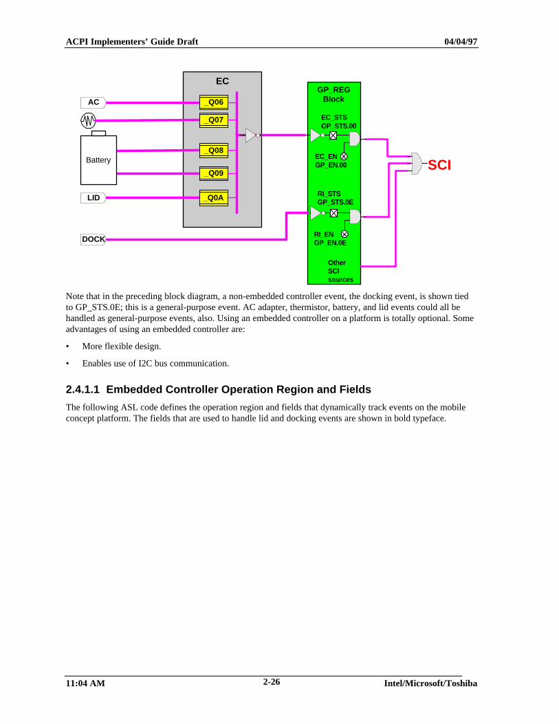
The following block diagram shows the relationships between the devices that are wired to the embeddedcontroller, the embedded controller queries, and the ACPI-specified General Purpose Register block which isthe source of an SCI. All embedded controller events raise the GP_STS.00 bit in the GP_REG block, and ifthat bit is enabled, and SCI occurs. The control method that handles an SCI from GP_STS.00 will notify theEC0 device, and the OS will query the EC to determine whether to run the _Q06, _Q07, _Q08, or _Q0Acontrol method depending upon whether the embedded controller event is from the AC adapter, thermistor,battery, or lid, respectively.
ACPI Implementers’ Guide Draft 04/04/97
11:04 AM Intel/Microsoft/Toshiba2-26
GP_REGBlock
EC_STSGP_STS.00
EC_ENGP_EN.00
OtherSCIsources
SCI
EC
RI_ENGP_EN.0E
RI_STSGP_STS.0ELID
DOCK
_Q0A
_Q09
_Q08
AC _Q06
_Q07
Battery
Note that in the preceding block diagram, a non-embedded controller event, the docking event, is shown tiedto GP_STS.0E; this is a general-purpose event. AC adapter, thermistor, battery, and lid events could all behandled as general-purpose events, also. Using an embedded controller on a platform is totally optional. Someadvantages of using an embedded controller are:
• More flexible design.
• Enables use of I2C bus communication.
2.4.1.1 Embedded Controller Operation Region and Fields
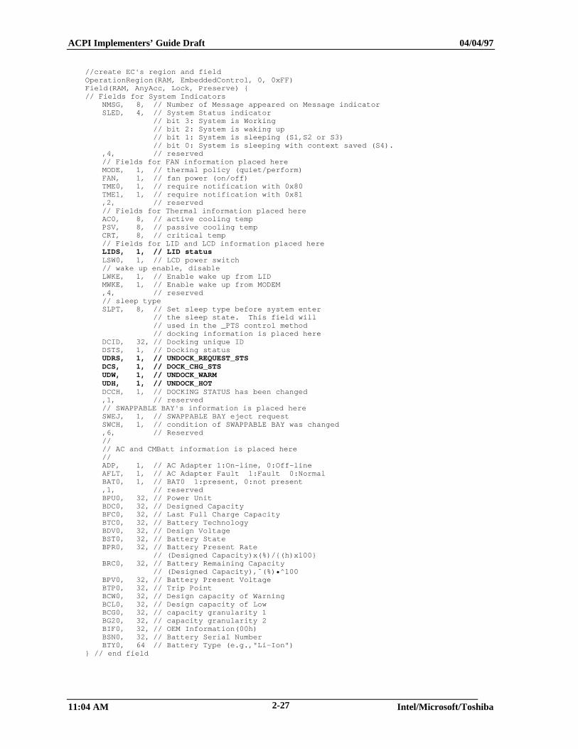
The following ASL code defines the operation region and fields that dynamically track events on the mobileconcept platform. The fields that are used to handle lid and docking events are shown in bold typeface.
ACPI Implementers’ Guide Draft 04/04/97
11:04 AM Intel/Microsoft/Toshiba2-27
//create EC's region and fieldOperationRegion(RAM, EmbeddedControl, 0, 0xFF)Field(RAM, AnyAcc, Lock, Preserve) {// Fields for System Indicators
NMSG, 8, // Number of Message appeared on Message indicatorSLED, 4, // System Status indicator
// bit 3: System is Working// bit 2: System is waking up// bit 1: System is sleeping (S1,S2 or S3)// bit 0: System is sleeping with context saved (S4).
,4, // reserved// Fields for FAN information placed hereMODE, 1, // thermal policy (quiet/perform)FAN, 1, // fan power (on/off)TME0, 1, // require notification with 0x80TME1, 1, // require notification with 0x81,2, // reserved// Fields for Thermal information placed hereAC0, 8, // active cooling tempPSV, 8, // passive cooling tempCRT, 8, // critical temp// Fields for LID and LCD information placed hereLIDS, 1, // LID statusLSW0, 1, // LCD power switch// wake up enable, disableLWKE, 1, // Enable wake up from LIDMWKE, 1, // Enable wake up from MODEM,4, // reserved// sleep typeSLPT, 8, // Set sleep type before system enter
// the sleep state. This field will// used in the _PTS control method// docking information is placed here
DCID, 32, // Docking unique IDDSTS, 1, // Docking statusUDRS, 1, // UNDOCK_REQUEST_STSDCS, 1, // DOCK_CHG_STSUDW, 1, // UNDOCK_WARMUDH, 1, // UNDOCK_HOTDCCH, 1, // DOCKING STATUS has been changed,1, // reserved// SWAPPABLE BAY's information is placed hereSWEJ, 1, // SWAPPABLE BAY eject requestSWCH, 1, // condition of SWAPPABLE BAY was changed,6, // Reserved//// AC and CMBatt information is placed here//ADP, 1, // AC Adapter 1:On-line, 0:Off-lineAFLT, 1, // AC Adapter Fault 1:Fault 0:NormalBAT0, 1, // BAT0 1:present, 0:not present,1, // reservedBPU0, 32, // Power UnitBDC0, 32, // Designed CapacityBFC0, 32, // Last Full Charge CapacityBTC0, 32, // Battery TechnologyBDV0, 32, // Design VoltageBST0, 32, // Battery StateBPR0, 32, // Battery Present Rate
// (Designed Capacity)x(%)/{(h)x100}BRC0, 32, // Battery Remaining Capacity
// (Designed Capacity)‚˜(%)•^100BPV0, 32, // Battery Present VoltageBTP0, 32, // Trip PointBCW0, 32, // Design capacity of WarningBCL0, 32, // Design capacity of LowBCG0, 32, // capacity granularity 1BG20, 32, // capacity granularity 2BIF0, 32, // OEM Information(00h)BSN0, 32, // Battery Serial NumberBTY0, 64 // Battery Type (e.g.,"Li-Ion")
} // end field
ACPI Implementers’ Guide Draft 04/04/97
11:04 AM Intel/Microsoft/Toshiba2-28
2.4.1.2 Handling Embedded Controller Lid Switch Events
A lid switch event happens when the mobile platform lid opens or closes.
The following objects in ACPI name space are involved in handling lid events as embedded controller events:
\GPE0 //General Purpose event_L00 //EC control Method to handle GP_STS.00...
\_SBLID //LID
_PRW //define wake device_LID //status of LID_PSW //enable/disable lid wake
.
.
.PCI0 //PCI root bridge (Host PCI bridge)
.
.
.ISA //PCI-ISA Bridge
EC0 //Embedded controller device..._Q09 //LID event notification...
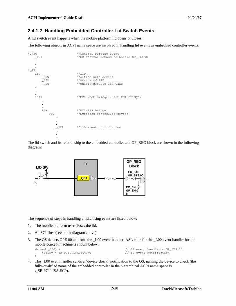
The lid switch and its relationship to the embedded controller and GP_REG block are shown in the followingdiagram:
GP_REGBlock
EC_STSGP_STS.00
EC_ENGP_EN.00
EC
EC_SCIRQ
LID SW
_Q0A
The sequence of steps in handling a lid closing event are listed below:
1. The mobile platform user closes the lid.
2. An SCI fires (see block diagram above).
3. The OS detects GPE 00 and runs the _L00 event handler. ASL code for the _L00 event handler for themobile concept machine is shown below.Method(_L00) { // GP event handle to GP_STS.00
Notify(\_SB.PCI0.ISA.EC0,0) // EC event notification}
4. The _L00 event handler sends a “device check” notification to the OS, naming the device to check (thefully-qualified name of the embedded controller in the hierarchical ACPI name space is\_SB.PCI0.ISA.EC0).
ACPI Implementers’ Guide Draft 04/04/97
11:04 AM Intel/Microsoft/Toshiba2-29
5. The OS’s policy for device checking an embedded controller is to query the device using the standardembedded controller query interface. Since this sequence started with the user closing the lid, theembedded controller returns the value of 0A in response to the query (see Figure 5-2).
6. This causes the OS to run the _Q0A event handler. ASL code for the _Q0A event handler is shown below.// Lid event - EC query value AMethod(_Q0A) {
Notify (\_SB.LID, 0x80) // notify LID status changed}
7. The _Q0A event handler sends a “lid status change” notification to the OS, naming the device object\_SB.LID.
8. The OS responds to this notification by running the _LID control method, which is defined in the ACPISpecification, Revision 1.0, to always return the status of the lid. The ASL code for the _LID method forthe mobile concept machine is:
Method(_LID) {Return( \_SB.PCI0.ISA.EC0.LIDS) // Status of the LID
}
9. “LIDS” is the name of a field in the embedded controller operation region which always contains thestatus of the lid. In this scenario, since the lid is closed, the value returned to the OS by the _LID methodis zero.
10. The OS carries out its “closed lid” policy.
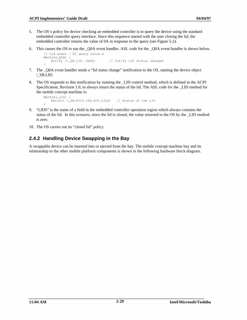
2.4.2 Handling Device Swapping in the Bay
A swappable device can be inserted into or ejected from the bay. The mobile concept machine bay and itsrelationship to the other mobile platform components is shown in the following hardware block diagram.
ACPI Implementers’ Guide Draft 04/04/97
11:04 AM Intel/Microsoft/Toshiba2-30
CPUCPU/
Memory/PCI Bridge
DRAM
L2
Prim
ary
PC
I BU
S
ISA
BU
S
Swappable Bay
BM-IDEcont.
HDD
HDD0
Systemcont.
Em
bedd
ed C
ontr
olle
r
Power Button(On/Off/Overide)
PCI-ISABridge
PIC,PIT,DMARTC,FDC,
UART,LPT
Primarychannel
Secondary channel
Eject Switch
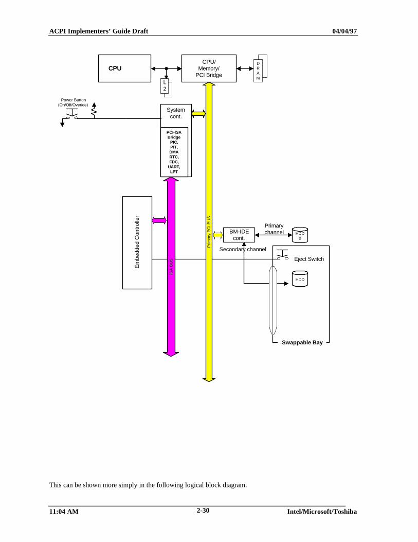
This can be shown more simply in the following logical block diagram.
ACPI Implementers’ Guide Draft 04/04/97
11:04 AM Intel/Microsoft/Toshiba2-31
Mobile System
Swappable Bay Area
2nd HDD
CD-ROM
HDDPrimaryIDEcontroller
SecondaryIDEcontroller
When a second HDD device is inserted in the Bay, two IDE controllers and two IDE HDD devices are active.Which IDE controller controls the primary channel and which IDE controller controls the secondary channelis encoded in the _ADR object under each IDE controller’s Device object in the ACPI name space, using thefollowing convention:
Name(_ADR, 0) //Primary channelName(_ADR, 1) //Secondary channelName(_ADR, 2) //Third channel (if needed)Name(_ADR, 3) //Fourth channel (if needed)
Which IDE device is the master and which is the slave is encoded in the _ADR object under each IDE HDD’sDevice object in the ACPI name space, using the following convention:
Name(_ADR, 0) //MasterName(_ADR, 1) //Slave
These conventions are used in the following block of code from the mobile concept machine’s ASL code:IDE //BusMaster IDE controller
_ADR //PCI address of BM-IDEPRIM //Primary Bus Master controller
_ADR //Primary channelBAY //swappable bay for 2nd HDD and CD-ROM
_ADR //Secondary channel_LCK //means ejectable
The following ASL code implements the namespace shown above.
ACPI Implementers’ Guide Draft 04/04/97
11:04 AM Intel/Microsoft/Toshiba2-32
Device(IDE) { //BM-IDE in system Name(_ADR, 0) //PCI address of BM-IDE
Method(_STA,0) { //Status of BM-IDE controller // If BM-IDE is functioning Return(0xF) // If IDE channel0 is disabled Return(0xD) }
Device(PRIM) { Name(_ADR,0) //Primary IDE channel
Method(_STA,0) { //Status of the primary channel // If IDE is exist and functioning Return(0xF) // If IDE channel0 is removed Return(0xD) } } // end PRIM Device(BAY) { //secondary IDE for BAY Name(_ADR, 1) //secondary IDE channel
Method(_STA,0) { //Status of secondary channel // If IDE is exist and functioning Return(0xF) // If IDE channel1 is removed Return(0xD) } Method(_LCK,1){ //means ejectable // Lock or unlock the SWAPPABLE BAY If (ARG0) { Store (0x1, \_SB.PCI0.ISA.EC0.SWEJ) //lock } Else { Store (0x0, \_SB.PCI0.ISA.EC0.SWEJ) //unlock } }
} // end BAY} // end IDE
Following is the Bay event handler code.// BAY changed event - EC query value BMethod(_Q0B) {
//When SWAPPABLE BAY is attached or unattached//this event will happen.Notify(\_SB.PCI0.ISA.BAY, 0) // bay event
}// BAY eject request event - EC query value CMethod(_Q0C) {
//When eject switch for SWAPPABLE BAY is pressed//this event will happen.Notify(\_SB.PCI0.ISA.BAY, 1) // bay eject request
}
2.4.3 Handling Dock Events
A dock event occurs when the user docks or undocks the mobile platform, or when the user makes anundocking request.
2.4.3.1 Handling Dock Events as General Purpose Events (GPEs)
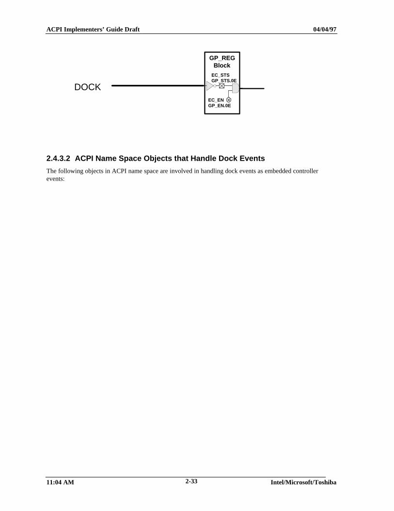
On the mobile concept machine, docking events are handled as a General Purpose Event (GPE). Dockingevents are tied to a bit in the GP_REG block as shown below.
ACPI Implementers’ Guide Draft 04/04/97
11:04 AM Intel/Microsoft/Toshiba2-33
GP_REGBlock
EC_STSGP_STS.0E
EC_ENGP_EN.0E
DOCK
2.4.3.2 ACPI Name Space Objects that Handle Dock Events
The following objects in ACPI name space are involved in handling dock events as embedded controllerevents:
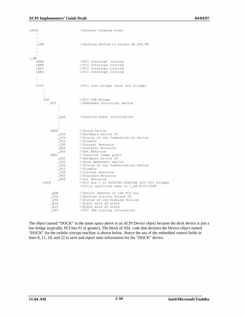
ACPI Implementers’ Guide Draft 04/04/97
11:04 AM Intel/Microsoft/Toshiba2-34
\GPE0 //General Purpose event..._L0E //docking method to handle GP_STS.0E...
\_SBLNKA //PCI Interrupt routingLNKB //PCI Interrupt routingLNKC //PCI Interrupt routingLNKD //PCI Interrupt routing...PCI0 //PCI root bridge (Host PCI bridge)
.
.
.ISA //PCI-ISA Bridge
EC0 //Embedded controller device..._Q0A //Docking event notification...
SND0 //Sound Device_HID //Hardware Device ID_STA //Status of the Communication Device_DIS //Disable_CRS //Current Resource_PRS //Possible Resource_SRS //Set Resource
SND1 //Joystick (Game port)_HID //Hardware Device ID_EJD //dock dependent device_STA //Status of the Communication Device_DIS //Disable_CRS //Current Resource_PRS //Possible Resource_SRS //Set Resource
DOCK //PCI Bus 1 of DOCKING STATION (PCI-PCI bridge)//Fully qualified name is \_SB.PCI0.DOCK
_ADR //Device address of the PCI bus_UID //Docking station Unique ID_STA //Status of the Docking Station_EJ0 //Eject with S0 state_EJ3 //Eject with S3 state_PRT //PCI IRQ routing information
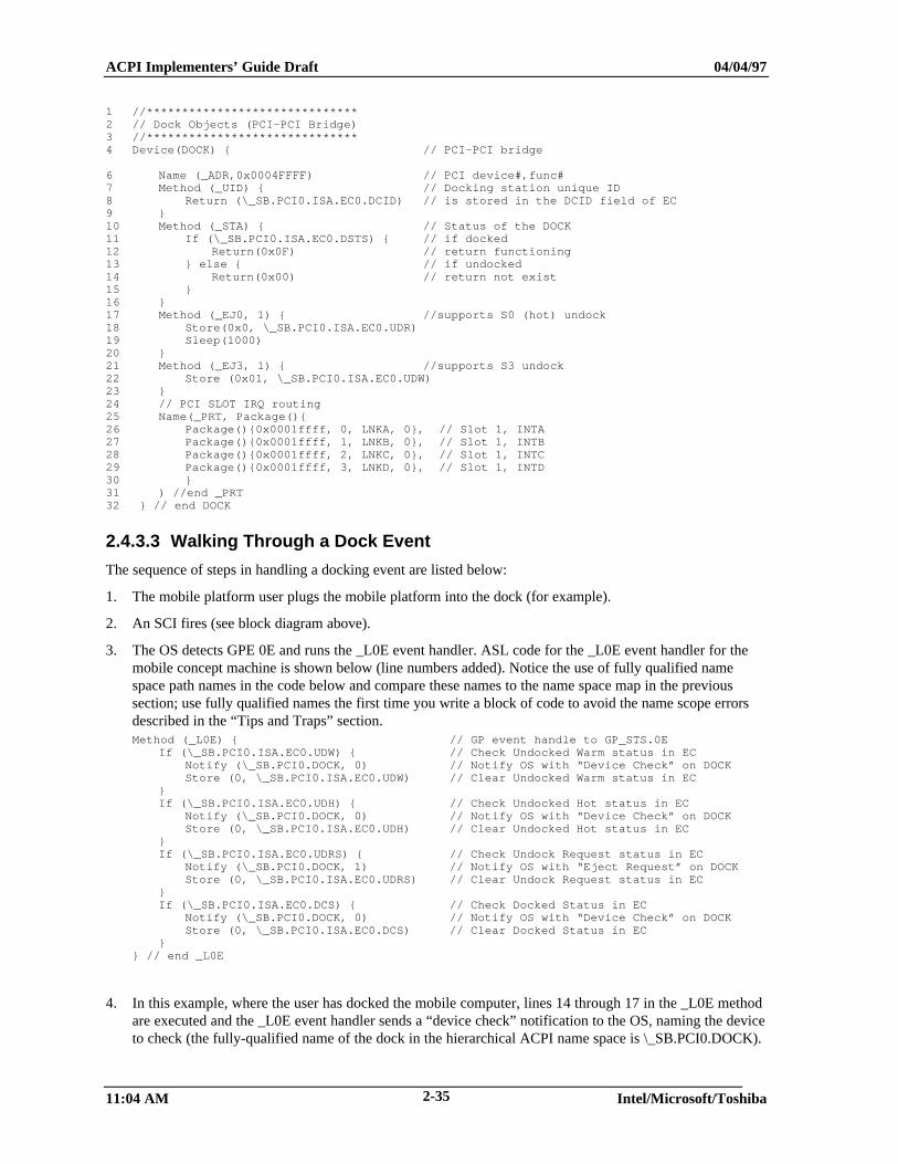
The object named “DOCK” in the name space above is an ACPI Device object because the dock device is just abus bridge (typically, PCI bus #1 or greater). The block of ASL code that declares the Device object named“DOCK” for the mobile concept machine is shown below. Notice the use of the embedded control fields inlines 8, 11, 18, and 22 to save and report state information for the “DOCK” device.
ACPI Implementers’ Guide Draft 04/04/97
11:04 AM Intel/Microsoft/Toshiba2-35
1 //******************************2 // Dock Objects (PCI-PCI Bridge)3 //******************************4 Device(DOCK) { // PCI-PCI bridge
6 Name (_ADR,0x0004FFFF) // PCI device#,func#7 Method (_UID) { // Docking station unique ID8 Return (\_SB.PCI0.ISA.EC0.DCID) // is stored in the DCID field of EC9 }10 Method (_STA) { // Status of the DOCK11 If (\_SB.PCI0.ISA.EC0.DSTS) { // if docked12 Return(0x0F) // return functioning13 } else { // if undocked14 Return(0x00) // return not exist15 }16 }17 Method (_EJ0, 1) { //supports S0 (hot) undock18 Store(0x0, \_SB.PCI0.ISA.EC0.UDR)19 Sleep(1000)20 }21 Method (_EJ3, 1) { //supports S3 undock22 Store (0x01, \_SB.PCI0.ISA.EC0.UDW)23 }24 // PCI SLOT IRQ routing25 Name(_PRT, Package(){26 Package(){0x0001ffff, 0, LNKA, 0}, // Slot 1, INTA27 Package(){0x0001ffff, 1, LNKB, 0}, // Slot 1, INTB28 Package(){0x0001ffff, 2, LNKC, 0}, // Slot 1, INTC29 Package(){0x0001ffff, 3, LNKD, 0}, // Slot 1, INTD30 }31 ) //end _PRT32 } // end DOCK
2.4.3.3 Walking Through a Dock Event
The sequence of steps in handling a docking event are listed below:
1. The mobile platform user plugs the mobile platform into the dock (for example).
2. An SCI fires (see block diagram above).
3. The OS detects GPE 0E and runs the _L0E event handler. ASL code for the _L0E event handler for themobile concept machine is shown below (line numbers added). Notice the use of fully qualified namespace path names in the code below and compare these names to the name space map in the previoussection; use fully qualified names the first time you write a block of code to avoid the name scope errorsdescribed in the “Tips and Traps” section.Method (_L0E) { // GP event handle to GP_STS.0E
If (\_SB.PCI0.ISA.EC0.UDW) { // Check Undocked Warm status in ECNotify (\_SB.PCI0.DOCK, 0) // Notify OS with “Device Check” on DOCKStore (0, \_SB.PCI0.ISA.EC0.UDW) // Clear Undocked Warm status in EC
}If (\_SB.PCI0.ISA.EC0.UDH) { // Check Undocked Hot status in EC
Notify (\_SB.PCI0.DOCK, 0) // Notify OS with “Device Check” on DOCKStore (0, \_SB.PCI0.ISA.EC0.UDH) // Clear Undocked Hot status in EC
}If (\_SB.PCI0.ISA.EC0.UDRS) { // Check Undock Request status in EC
Notify (\_SB.PCI0.DOCK, 1) // Notify OS with “Eject Request” on DOCKStore (0, \_SB.PCI0.ISA.EC0.UDRS) // Clear Undock Request status in EC
}If (\_SB.PCI0.ISA.EC0.DCS) { // Check Docked Status in EC
Notify (\_SB.PCI0.DOCK, 0) // Notify OS with “Device Check” on DOCKStore (0, \_SB.PCI0.ISA.EC0.DCS) // Clear Docked Status in EC
}} // end _L0E
4. In this example, where the user has docked the mobile computer, lines 14 through 17 in the _L0E methodare executed and the _L0E event handler sends a “device check” notification to the OS, naming the deviceto check (the fully-qualified name of the dock in the hierarchical ACPI name space is \_SB.PCI0.DOCK).
ACPI Implementers’ Guide Draft 04/04/97
11:04 AM Intel/Microsoft/Toshiba2-36
5. The OS runs its docking policy.
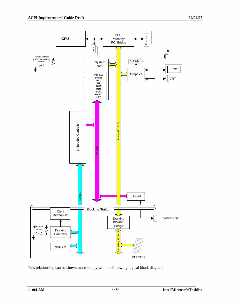
2.4.4 Device Status Changes
The status of various devices can change. The most obvious example of this on the mobile concept machine isthe joystick device. A joystick is only available to the Mobile concept machine user when the mobile platformis docked, as shown in the following hardware block diagram.
ACPI Implementers’ Guide Draft 04/04/97
11:04 AM Intel/Microsoft/Toshiba2-37
CPUCPU/
Memory/PCI Bridge
DRAM
Sound
Graphics
L2
Prim
ary
PC
I BU
S
ISA
BU
S
I2C
BU
S
VRAM
CRT
DockingController
DockingPCI/PCIBridge
Sec
onda
ry P
CI B
US
PCI Slots
NVRAM
Eject SW
Joystick port
Systemcont.
Em
bedd
ed C
ontr
olle
r
Power Button(On/Off/Overide)
EjectMechanism
LCD
PCI-ISABridge
PIC,PIT,DMARTC,FDC,
UART,LPT
Docking Station
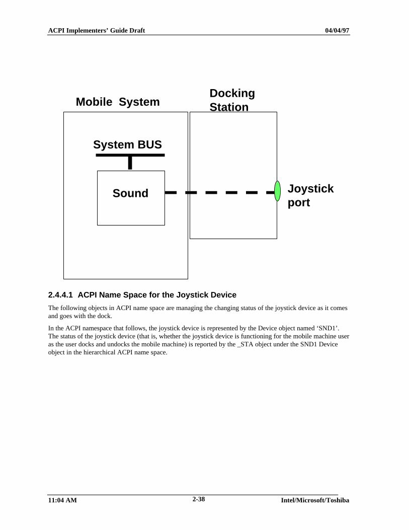
This relationship can be shown more simply with the following logical block diagram.
ACPI Implementers’ Guide Draft 04/04/97
11:04 AM Intel/Microsoft/Toshiba2-38
Sound
System BUS
Mobile SystemDockingStation
Joystickport
2.4.4.1 ACPI Name Space for the Joystick Device
The following objects in ACPI name space are managing the changing status of the joystick device as it comesand goes with the dock.
In the ACPI namespace that follows, the joystick device is represented by the Device object named ‘SND1’.The status of the joystick device (that is, whether the joystick device is functioning for the mobile machine useras the user docks and undocks the mobile machine) is reported by the _STA object under the SND1 Deviceobject in the hierarchical ACPI name space.
ACPI Implementers’ Guide Draft 04/04/97
11:04 AM Intel/Microsoft/Toshiba2-39
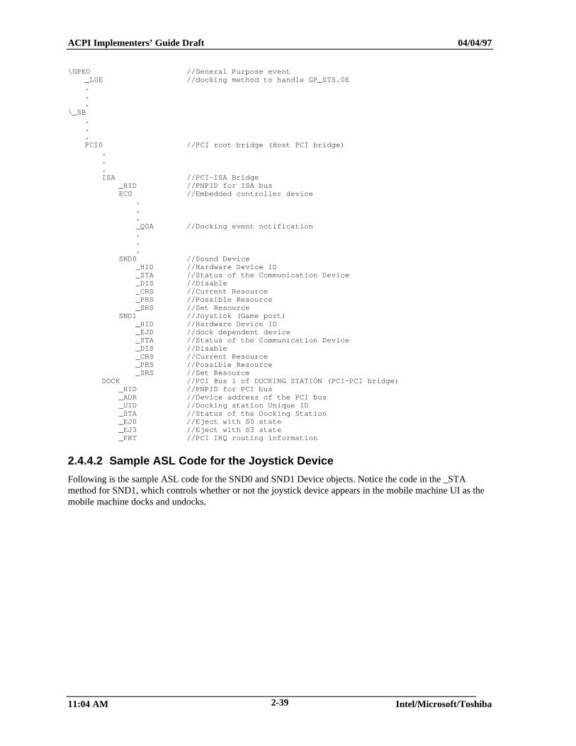
\GPE0 //General Purpose event_L0E //docking method to handle GP_STS.0E...
\_SB...PCI0 //PCI root bridge (Host PCI bridge)
.
.
.ISA //PCI-ISA Bridge
_HID //PNPID for ISA busEC0 //Embedded controller device
.
.
._Q0A //Docking event notification...
SND0 //Sound Device_HID //Hardware Device ID_STA //Status of the Communication Device_DIS //Disable_CRS //Current Resource_PRS //Possible Resource_SRS //Set Resource
SND1 //Joystick (Game port)_HID //Hardware Device ID_EJD //dock dependent device_STA //Status of the Communication Device_DIS //Disable_CRS //Current Resource_PRS //Possible Resource_SRS //Set Resource
DOCK //PCI Bus 1 of DOCKING STATION (PCI-PCI bridge)_HID //PNPID for PCI bus_ADR //Device address of the PCI bus_UID //Docking station Unique ID_STA //Status of the Docking Station_EJ0 //Eject with S0 state_EJ3 //Eject with S3 state_PRT //PCI IRQ routing information
2.4.4.2 Sample ASL Code for the Joystick Device
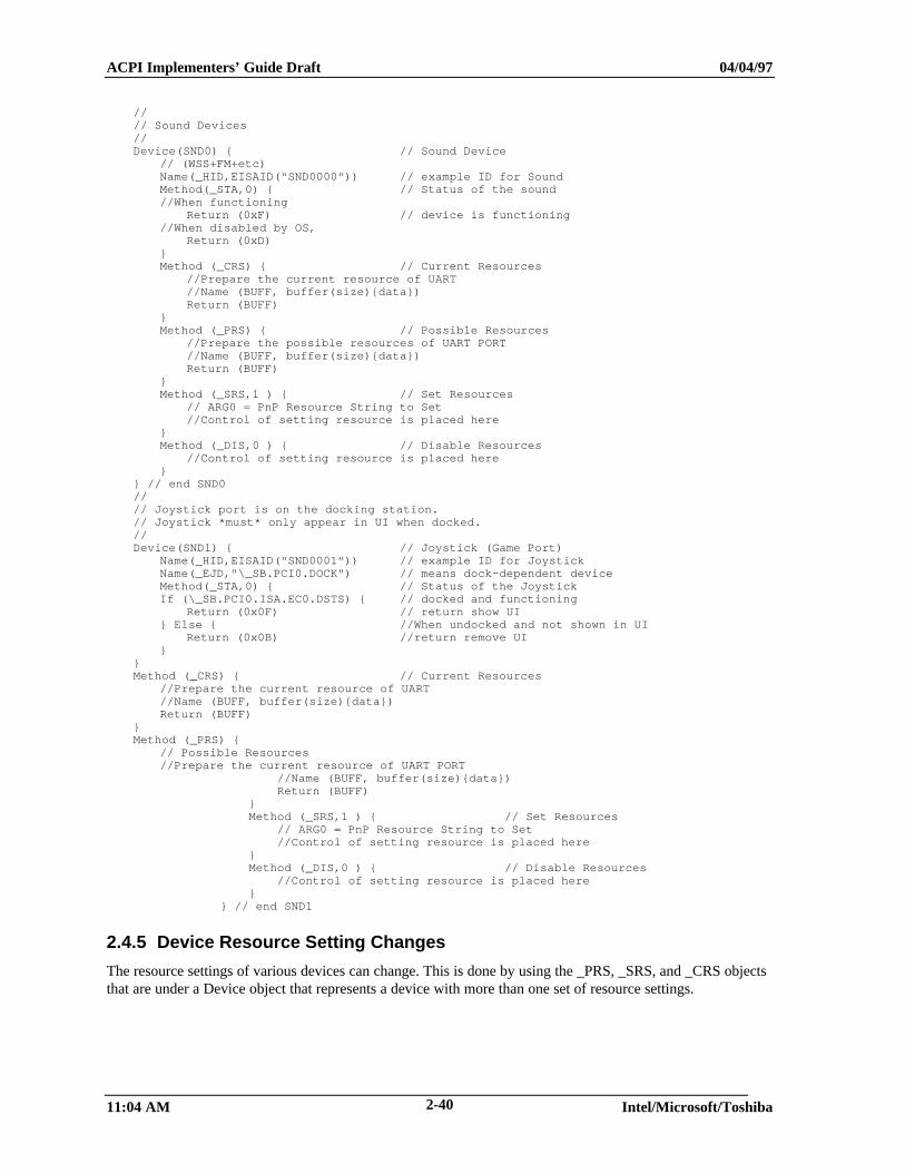
Following is the sample ASL code for the SND0 and SND1 Device objects. Notice the code in the _STAmethod for SND1, which controls whether or not the joystick device appears in the mobile machine UI as themobile machine docks and undocks.
ACPI Implementers’ Guide Draft 04/04/97
11:04 AM Intel/Microsoft/Toshiba2-40
//// Sound Devices//Device(SND0) { // Sound Device
// (WSS+FM+etc)Name(_HID,EISAID("SND0000")) // example ID for SoundMethod(_STA,0) { // Status of the sound//When functioning
Return (0xF) // device is functioning//When disabled by OS,
Return (0xD)}Method (_CRS) { // Current Resources
//Prepare the current resource of UART//Name (BUFF, buffer(size){data})Return (BUFF)
}Method (_PRS) { // Possible Resources
//Prepare the possible resources of UART PORT//Name (BUFF, buffer(size){data})Return (BUFF)
}Method (_SRS,1 ) { // Set Resources
// ARG0 = PnP Resource String to Set//Control of setting resource is placed here
}Method (_DIS,0 ) { // Disable Resources
//Control of setting resource is placed here}
} // end SND0//// Joystick port is on the docking station.// Joystick *must* only appear in UI when docked.//Device(SND1) { // Joystick (Game Port)
Name(_HID,EISAID("SND0001")) // example ID for JoystickName(_EJD,"\_SB.PCI0.DOCK") // means dock-dependent deviceMethod(_STA,0) { // Status of the JoystickIf (\_SB.PCI0.ISA.EC0.DSTS) { // docked and functioning
Return (0x0F) // return show UI} Else { //When undocked and not shown in UI
Return (0x0B) //return remove UI}
}Method (_CRS) { // Current Resources
//Prepare the current resource of UART//Name (BUFF, buffer(size){data})Return (BUFF)
}Method (_PRS) {
// Possible Resources//Prepare the current resource of UART PORT
//Name (BUFF, buffer(size){data}) Return (BUFF) } Method (_SRS,1 ) { // Set Resources // ARG0 = PnP Resource String to Set //Control of setting resource is placed here } Method (_DIS,0 ) { // Disable Resources //Control of setting resource is placed here } } // end SND1
2.4.5 Device Resource Setting Changes
The resource settings of various devices can change. This is done by using the _PRS, _SRS, and _CRS objectsthat are under a Device object that represents a device with more than one set of resource settings.
ACPI Implementers’ Guide Draft 04/04/97
11:04 AM Intel/Microsoft/Toshiba2-41
2.5 Complete Mobile Concept Machine ACPI Name Space
This section shows the hierarchy of objects in ACPI name space that models the block diagram shown above.
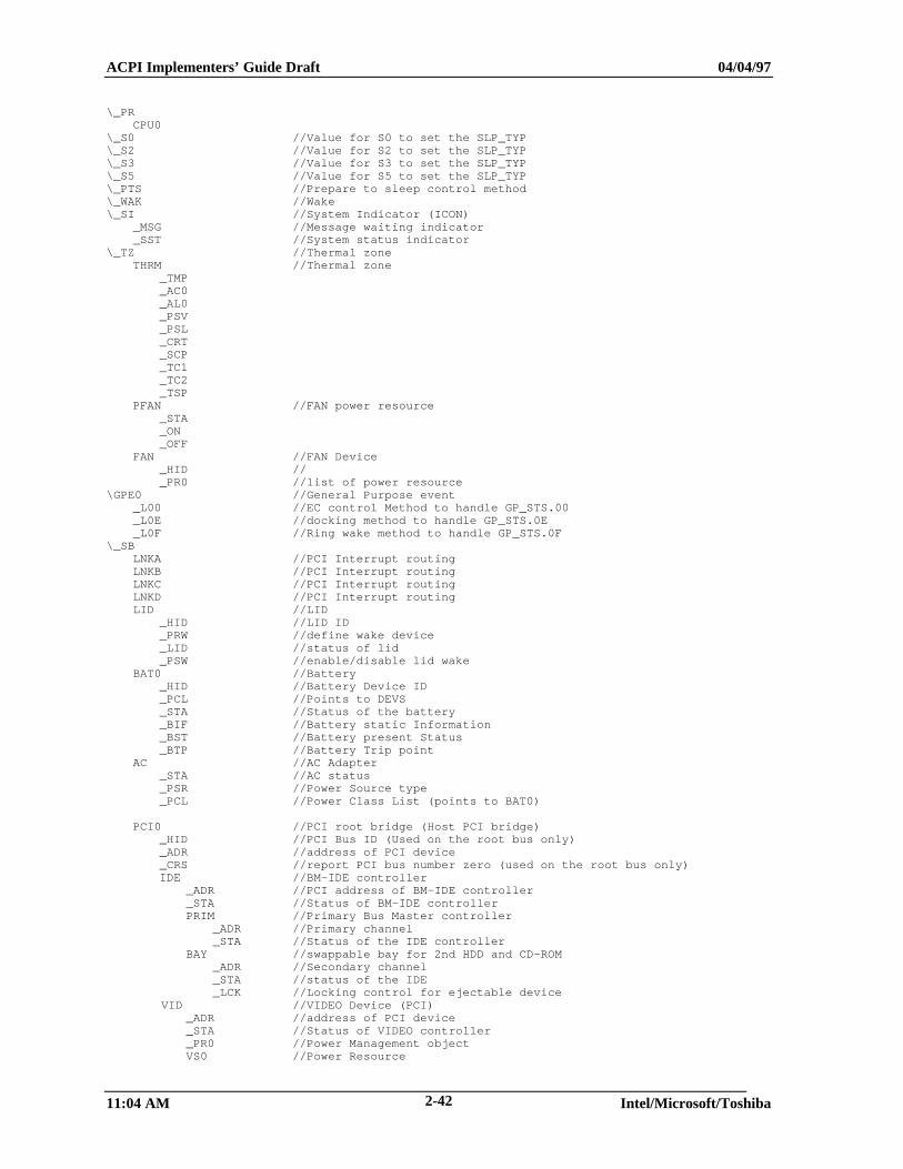
ACPI Implementers’ Guide Draft 04/04/97
11:04 AM Intel/Microsoft/Toshiba2-42
\_PRCPU0
\_S0 //Value for S0 to set the SLP_TYP\_S2 //Value for S2 to set the SLP_TYP\_S3 //Value for S3 to set the SLP_TYP\_S5 //Value for S5 to set the SLP_TYP\_PTS //Prepare to sleep control method\_WAK //Wake\_SI //System Indicator (ICON)
_MSG //Message waiting indicator_SST //System status indicator
\_TZ //Thermal zoneTHRM //Thermal zone
_TMP_AC0_AL0_PSV_PSL_CRT_SCP_TC1_TC2_TSP
PFAN //FAN power resource_STA_ON_OFF
FAN //FAN Device_HID //_PR0 //list of power resource
\GPE0 //General Purpose event_L00 //EC control Method to handle GP_STS.00_L0E //docking method to handle GP_STS.0E_L0F //Ring wake method to handle GP_STS.0F
\_SBLNKA //PCI Interrupt routingLNKB //PCI Interrupt routingLNKC //PCI Interrupt routingLNKD //PCI Interrupt routingLID //LID
_HID //LID ID_PRW //define wake device_LID //status of lid_PSW //enable/disable lid wake
BAT0 //Battery_HID //Battery Device ID_PCL //Points to DEVS_STA //Status of the battery_BIF //Battery static Information_BST //Battery present Status_BTP //Battery Trip point
AC //AC Adapter_STA //AC status_PSR //Power Source type_PCL //Power Class List (points to BAT0)
PCI0 //PCI root bridge (Host PCI bridge)_HID //PCI Bus ID (Used on the root bus only)_ADR //address of PCI device_CRS //report PCI bus number zero (used on the root bus only)IDE //BM-IDE controller
_ADR //PCI address of BM-IDE controller_STA //Status of BM-IDE controllerPRIM //Primary Bus Master controller
_ADR //Primary channel_STA //Status of the IDE controller
BAY //swappable bay for 2nd HDD and CD-ROM_ADR //Secondary channel_STA //status of the IDE_LCK //Locking control for ejectable device
VID //VIDEO Device (PCI)_ADR //address of PCI device_STA //Status of VIDEO controller_PR0 //Power Management objectVS0 //Power Resource
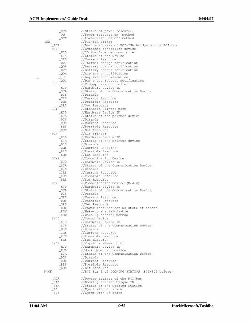
ACPI Implementers’ Guide Draft 04/04/97
11:04 AM Intel/Microsoft/Toshiba2-43
_STA //Status of power resource_ON //Power resource on method_OFF //Power resource off method
ISA //PCI-ISA Bridge_ADR //Device address of PCI-ISA bridge on the PCI busEC0 //Embedded controller device
_HID //ID for Embedded controller_STA //Status of the Device_CRS //Current Resource_Q07 //Thermal change notification_Q08 //Battery change notification_Q09 //Battery status notification_Q0A //LID event notification
_ _Q0B //bay event notification _Q0C //bay eject request notification
FDC0 //Floppy Disk controller_HID //Hardware Device ID_STA //Status of the Communication Device_DIS //Disable_CRS //Current Resource_PRS //Possible Resource_SRS //Set Resource
LPT //Standard Printer port_HID //Hardware Device ID_STA //Status of the printer device_DIS //Disable_CRS //Current Resource_PRS //Possible Resource_SRS //Set Resource
ECP //ECP Printer_HID //Hardware Device ID_STA //Status of the printer device_DIS //Disable_CRS //Current Resource_PRS //Possible Resource_SRS //Set Resource
COMA //Communication Device_HID //Hardware Device ID_STA //Status of the Communication Device_DIS //Disable_CRS //Current Resource_PRS //Possible Resource_SRS //Set Resource
MDM0 //Communication Device (Modem)_HID //Hardware Device ID_STA //Status of the Communication Device_DIS //Disable_CRS //Current Resource_PRS //Possible Resource_SRS //Set Resource_PR0 //Power resource for D0 state if needed_PSW //Wake-up enable/disable_PRW //Wake-up control method
SND0 //Sound Device_HID //Hardware Device ID_STA //Status of the Communication Device_DIS //Disable_CRS //Current Resource_PRS //Possible Resource_SRS //Set Resource
SND1 //Joystick (Game port)_HID //Hardware Device ID_EJD //dock dependent device_STA //Status of the Communication Device_DIS //Disable_CRS //Current Resource_PRS //Possible Resource_SRS //Set Resource
DOCK //PCI Bus 1 of DOCKING STATION (PCI-PCI bridge)
_ADR //Device address of the PCI bus_UID //Docking station Unique ID_STA //Status of the Docking Station_EJ0 //Eject with S0 state_EJ3 //Eject with S3 state
ACPI Implementers’ Guide Draft 04/04/97
11:04 AM Intel/Microsoft/Toshiba2-44
_PRT //PCI IRQ routing information
2.6 Complete Listing if the Mobile Concept Machine ASL Code
This section shows all of the mobile concept machine DSDT ASL code in one listing. When the ASL codelisted below was run through the most recent version of the Microsoft-provided ASL compiler, it produced anAML byte stream just under 4000 bytes in size.
Note that the following ASL code is an example only, for illustrative purposes.
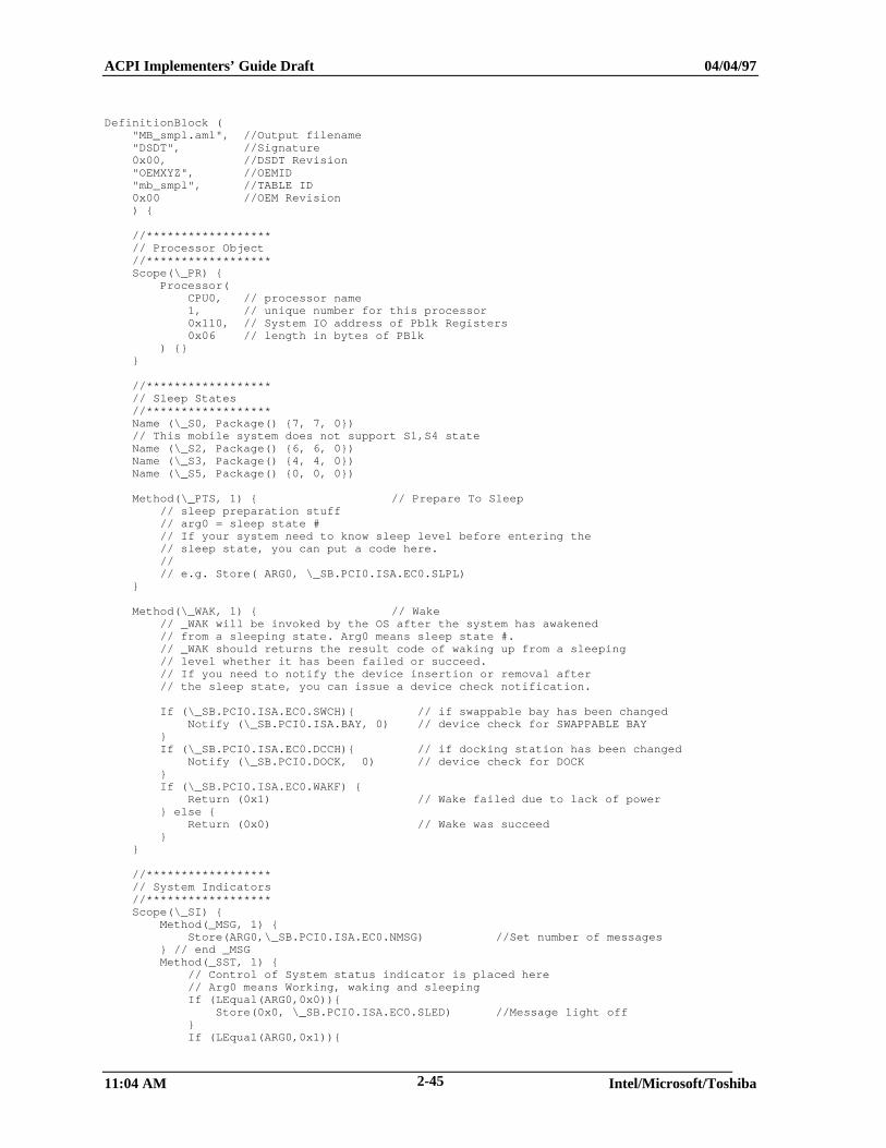
ACPI Implementers’ Guide Draft 04/04/97
11:04 AM Intel/Microsoft/Toshiba2-45
DefinitionBlock ( "MB_smpl.aml", //Output filename "DSDT", //Signature 0x00, //DSDT Revision "OEMXYZ", //OEMID "mb_smpl", //TABLE ID 0x00 //OEM Revision ) {
//****************** // Processor Object //****************** Scope(\_PR) { Processor( CPU0, // processor name 1, // unique number for this processor 0x110, // System IO address of Pblk Registers 0x06 // length in bytes of PBlk ) {} }
//****************** // Sleep States //****************** Name (\_S0, Package() {7, 7, 0}) // This mobile system does not support S1,S4 state Name (\_S2, Package() {6, 6, 0}) Name (\_S3, Package() {4, 4, 0}) Name (\_S5, Package() {0, 0, 0})
Method(\_PTS, 1) { // Prepare To Sleep // sleep preparation stuff // arg0 = sleep state # // If your system need to know sleep level before entering the // sleep state, you can put a code here. // // e.g. Store( ARG0, \_SB.PCI0.ISA.EC0.SLPL) }
Method(\_WAK, 1) { // Wake // _WAK will be invoked by the OS after the system has awakened // from a sleeping state. Arg0 means sleep state #. // _WAK should returns the result code of waking up from a sleeping // level whether it has been failed or succeed. // If you need to notify the device insertion or removal after // the sleep state, you can issue a device check notification.
If (\_SB.PCI0.ISA.EC0.SWCH){ // if swappable bay has been changed Notify (\_SB.PCI0.ISA.BAY, 0) // device check for SWAPPABLE BAY } If (\_SB.PCI0.ISA.EC0.DCCH){ // if docking station has been changed Notify (\_SB.PCI0.DOCK, 0) // device check for DOCK } If (\_SB.PCI0.ISA.EC0.WAKF) { Return (0x1) // Wake failed due to lack of power } else { Return (0x0) // Wake was succeed } }
//****************** // System Indicators //****************** Scope(\_SI) { Method(_MSG, 1) { Store(ARG0,\_SB.PCI0.ISA.EC0.NMSG) //Set number of messages } // end _MSG Method(_SST, 1) { // Control of System status indicator is placed here // Arg0 means Working, waking and sleeping If (LEqual(ARG0,0x0)){ Store(0x0, \_SB.PCI0.ISA.EC0.SLED) //Message light off } If (LEqual(ARG0,0x1)){
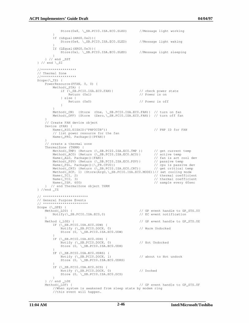
ACPI Implementers’ Guide Draft 04/04/97
11:04 AM Intel/Microsoft/Toshiba2-46
Store(0x8, \_SB.PCI0.ISA.EC0.SLED) //Message light working } If (LEqual(ARG0,0x2)){ Store(0x4, \_SB.PCI0.ISA.EC0.SLED) //Message light waking } If (LEqual(ARG0,0x3)){ Store(0x1, \_SB.PCI0.ISA.EC0.SLED) //Message light sleeping } } // end _SST } // end \_SI
//****************** // Thermal Zone //****************** Scope(\_TZ) { PowerResource(PFAN, 0, 0) { Method(_STA) { if (\_SB.PCI0.ISA.EC0.FAN){ // check power state Return (0x1) // Power is on } else { Return (0x0) // Power is off } } Method(_ON) {Store (One, \_SB.PCI0.ISA.EC0.FAN)} // turn on fan Method(_OFF) {Store (Zero,\_SB.PCI0.ISA.EC0.FAN)} // turn off fan } // Create FAN device object Device (FAN) { Name(_HID,EISAID("PNP0C0B")) // PNP ID for FAN // list power resource for the fan Name(_PR0, Package(){PFAN}) } // create a thermal zone ThermalZone (THRM) { Method(_TMP) {Return (\_SB.PCI0.ISA.EC0.TMP )} // get current temp Method(_AC0) {Return (\_SB.PCI0.ISA.EC0.AC0)} // active temp Name(_AL0, Package(){FAN}) // fan is act cool dev Method(_PSV) {Return (\_SB.PCI0.ISA.EC0.PSV)} // passive temp Name(_PSL, Package(){\_PR.CPU0}) // cpu is passive dev Method(_CRT) {Return (\_SB.PCI0.ISA.EC0.CRT)} // get critical temp Method(_SCP, 1) {Store(Arg0,\_SB.PCI0.ISA.EC0.MODE)}// set cooling mode Name(_TC1, 2) // thermal coefficient Name(_TC2, 3) // thermal coefficient Name(_TSP, 600) // sample every 60sec } // end ThermalZone object THRM } //end _TZ
// *********************** // General Purpose Events // *********************** Scope (\_GPE) { Method(_L00) { // GP event handle to GP_STS.00 Notify(\_SB.PCI0.ISA.EC0,0) // EC event notification } Method (_L0E) { // GP event handle to GP_STS.0E IF (\_SB.PCI0.ISA.EC0.UDW) { Notify (\_SB.PCI0.DOCK, 0) // Warm Undocked Store (0, \_SB.PCI0.ISA.EC0.UDW) } IF (\_SB.PCI0.ISA.EC0.UDH) { Notify (\_SB.PCI0.DOCK, 0) // Hot Undocked Store (0, \_SB.PCI0.ISA.EC0.UDH) } IF (\_SB.PCI0.ISA.EC0.UDRS) { Notify (\_SB.PCI0.DOCK, 1) // about to Hot undock Store (0, \_SB.PCI0.ISA.EC0.UDRS) } IF (\_SB.PCI0.ISA.EC0.DCS) { Notify (\_SB.PCI0.DOCK, 0) // Docked Store (0, \_SB.PCI0.ISA.EC0.DCS) } } // end _L0E Method(_L0F) { // GP event handle to GP_STS.0F //When system is awakened from sleep state by modem ring //this event will happen.
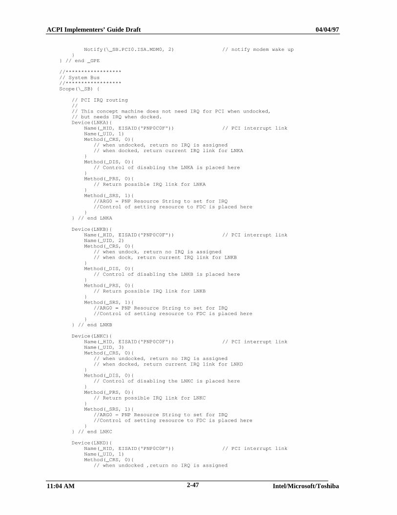
ACPI Implementers’ Guide Draft 04/04/97
11:04 AM Intel/Microsoft/Toshiba2-47
Notify(\_SB.PCI0.ISA.MDM0, 2) // notify modem wake up } } // end _GPE
//****************** // System Bus //****************** Scope(\_SB) {
// PCI IRQ routing // // This concept machine does not need IRQ for PCI when undocked, // but needs IRQ when docked. Device(LNKA){ Name(_HID, EISAID("PNP0C0F")) // PCI interrupt link Name(_UID, 1) Method(_CRS, 0){
// when undocked, return no IRQ is assigned// when docked, return current IRQ link for LNKA
} Method(_DIS, 0){
// Control of disabling the LNKA is placed here } Method(_PRS, 0){
// Return possible IRQ link for LNKA } Method(_SRS, 1){
//ARG0 = PNP Resource String to set for IRQ//Control of setting resource to FDC is placed here
} } // end LNKA
Device(LNKB){ Name(_HID, EISAID("PNP0C0F")) // PCI interrupt link Name(_UID, 2) Method(_CRS, 0){
// when undock, return no IRQ is assigned// when dock, return current IRQ link for LNKB
} Method(_DIS, 0){
// Control of disabling the LNKB is placed here } Method(_PRS, 0){
// Return possible IRQ link for LNKB } Method(_SRS, 1){
//ARG0 = PNP Resource String to set for IRQ//Control of setting resource to FDC is placed here
} } // end LNKB
Device(LNKC){ Name(_HID, EISAID("PNP0C0F")) // PCI interrupt link Name(_UID, 3) Method(_CRS, 0){
// when undocked, return no IRQ is assigned// when docked, return current IRQ link for LNKD
} Method(_DIS, 0){
// Control of disabling the LNKC is placed here } Method(_PRS, 0){
// Return possible IRQ link for LNKC } Method(_SRS, 1){
//ARG0 = PNP Resource String to set for IRQ//Control of setting resource to FDC is placed here
} } // end LNKC
Device(LNKD){ Name(_HID, EISAID("PNP0C0F")) // PCI interrupt link Name(_UID, 1) Method(_CRS, 0){
// when undocked ,return no IRQ is assigned
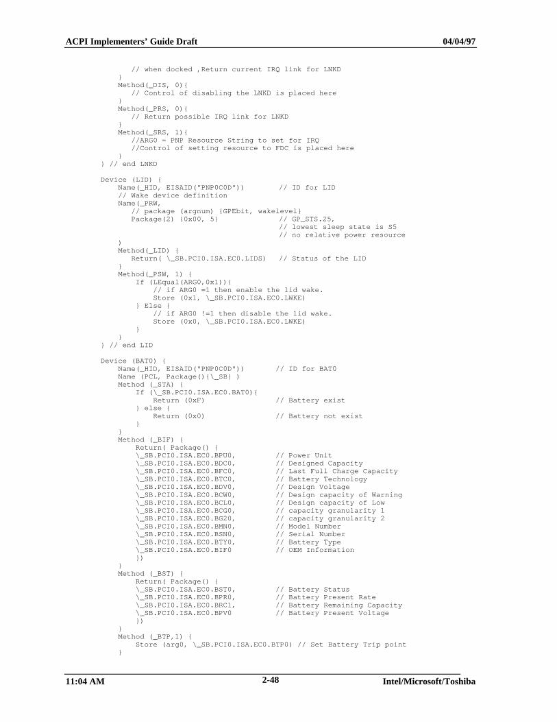
ACPI Implementers’ Guide Draft 04/04/97
11:04 AM Intel/Microsoft/Toshiba2-48
// when docked ,Return current IRQ link for LNKD } Method(_DIS, 0){
// Control of disabling the LNKD is placed here } Method(_PRS, 0){
// Return possible IRQ link for LNKD } Method(_SRS, 1){
//ARG0 = PNP Resource String to set for IRQ//Control of setting resource to FDC is placed here
} } // end LNKD
Device (LID) { Name(_HID, EISAID("PNP0C0D")) // ID for LID // Wake device definition Name(_PRW,
// package (argnum) {GPEbit, wakelevel}Package(2) {0x00, 5} // GP_STS.25,
// lowest sleep state is S5// no relative power resource
) Method(_LID) {
Return( \_SB.PCI0.ISA.EC0.LIDS) // Status of the LID } Method(_PSW, 1) { If (LEqual(ARG0,0x1)){ // if ARG0 =1 then enable the lid wake. Store (0x1, \_SB.PCI0.ISA.EC0.LWKE) } Else { // if ARG0 !=1 then disable the lid wake. Store (0x0, \_SB.PCI0.ISA.EC0.LWKE) } } } // end LID
Device (BAT0) { Name(_HID, EISAID("PNP0C0D")) // ID for BAT0 Name (PCL, Package(){\_SB} ) Method (_STA) { If (\_SB.PCI0.ISA.EC0.BAT0){ Return (0xF) // Battery exist } else { Return (0x0) // Battery not exist } } Method (_BIF) { Return( Package() { \_SB.PCI0.ISA.EC0.BPU0, // Power Unit \_SB.PCI0.ISA.EC0.BDC0, // Designed Capacity \_SB.PCI0.ISA.EC0.BFC0, // Last Full Charge Capacity \_SB.PCI0.ISA.EC0.BTC0, // Battery Technology \_SB.PCI0.ISA.EC0.BDV0, // Design Voltage \_SB.PCI0.ISA.EC0.BCW0, // Design capacity of Warning \_SB.PCI0.ISA.EC0.BCL0, // Design capacity of Low \_SB.PCI0.ISA.EC0.BCG0, // capacity granularity 1 \_SB.PCI0.ISA.EC0.BG20, // capacity granularity 2 \_SB.PCI0.ISA.EC0.BMN0, // Model Number \_SB.PCI0.ISA.EC0.BSN0, // Serial Number \_SB.PCI0.ISA.EC0.BTY0, // Battery Type \_SB.PCI0.ISA.EC0.BIF0 // OEM Information }) } Method (_BST) { Return( Package() { \_SB.PCI0.ISA.EC0.BST0, // Battery Status \_SB.PCI0.ISA.EC0.BPR0, // Battery Present Rate \_SB.PCI0.ISA.EC0.BRC1, // Battery Remaining Capacity \_SB.PCI0.ISA.EC0.BPV0 // Battery Present Voltage }) } Method (_BTP,1) { Store (arg0, \_SB.PCI0.ISA.EC0.BTP0) // Set Battery Trip point }
ACPI Implementers’ Guide Draft 04/04/97
11:04 AM Intel/Microsoft/Toshiba2-49
} //end BAT0
Device (AC) { // AC Adapter Name (_PCL, Package(){\_SB}) // Power Class List Method (_PSR) { // 0=Off-line, 1=On-line Return (\_SB.PCI0.ISA.EC0.ADP) // Power Source type } Method (_STA) { If (\_SB.PCI0.ISA.EC0.AFLT){ // Return Fault status of AC Return (0xF) // AC Adapter exists } Else { Return (0x0) // AC Adapter does not exist } } } //end AC
//****************** // HOST PCI BUS //****************** Device(PCI0) { // Root PCI Bus Name(_HID, EISAID("PNP0A03")) // _HID for root PCI bus Name(_ADR,0x0000000) // PCI Device#0, functoin#0 Method (_CRS,0) { // _CRS for PCI bus number
// PCI bus number as Zero by word address descriptor// Return( WORDBusNumber(,,,,0,0,0,0) )
} // end _CRS
// PCI IRQ routing // No internal PCI devices use IRQ on this concept machine. // Therefore, no needs to put _PRT here. // if your PCI device consume IRQ , you need describe it with _PRT
//********************************************** // BusMaster IDE //********************************************** Device(IDE) { //BM-IDE in system Name(_ADR, 0) //PCI address of BM-IDE
Method(_STA,0) { //Status of BM-IDE controller // If BM-IDE is functioning Return(0xF) // If IDE channel0 is disabled Return(0xD) }
Device(PRIM) { Name(_ADR,0) //Primary IDE channel
Method(_STA,0) { //Status of the primary channel // If IDE is exist and functioning Return(0xF) // If IDE channel0 is removed Return(0xD) } } // end PRIM
Device(BAY) { //secondary IDE for BAY Name(_ADR, 1) //secondary IDE channel
Method(_STA,0) { //Status of secondary channel // If IDE is exist and functioning Return(0xF) // If IDE channel1 is removed Return(0xD) } Method(_LCK,1){ //means ejectable // Lock or unlock the SWAPPABLE BAY If (ARG0) { Store (0x1, \_SB.PCI0.ISA.EC0.SWEJ) //lock } Else { Store (0x0, \_SB.PCI0.ISA.EC0.SWEJ) //unlock } }
} // end BAY } // end IDE
//**********************************************
ACPI Implementers’ Guide Draft 04/04/97
11:04 AM Intel/Microsoft/Toshiba2-50
// Video system has a power save switch for LCD. //********************************************** Device (VID0) { Name(_ADR,0x00020000) //Device#2, Function#0 Method(_STA,0) { //_STA for PCI VIDEO Return (0xF) // VIDEO is functioning } //This system has a LCD power save switch (VS0) //VS0 should be on during D0 state. Name (_PR0, Package(){VS0}) //VS0 needs on at D0 state //VS0 does not need a D1,D2, //and D3 state. PowerResource(VS0, 0, 0) { Method(_STA) { If (\_SB.PCI0.ISA.EC0.LSW0){
Return (0x1) // Power is on } Else {
Return (0x0) // Power is off } } Method(_ON) {Store (One ,\_SB.PCI0.ISA.EC0.LSW0) } Method(_OFF) {Store (Zero,\_SB.PCI0.ISA.EC0.LSW0) } } //end Power Resource }
// Other PCI devices don't appear as there is no value // added hardware and system uses the standard PCI PnP and standard // driver support power management
//****************** // PCI-ISA Bridge //****************** Device(ISA) { Name(_HID, EISAID("PNP0A00")) //ID for ISA bus
Device(EC0) { //Embedded ControllerName(_HID, EISAID("PNP0C09")) //ID for ECMethod(_STA,0) { //Status of the EC
Return(0xF) //EC is functioning}Method (_CRS ,0) {
// Store the Current Resource into Buff // Name (BUFF, buffer(size){data}) Return(BUFF)
} // end _CRS
}//create EC's region and fieldOperationRegion(RAM, EmbeddedControl, 0, 0xFF)
Field(RAM, AnyAcc, Lock, Preserve) {// Fields for System IndicatorsNMSG, 8, // Number of Message appeared on Message indicatorSLED, 4, // System Status indicator
// bit 3: System is Working// bit 2: System is waking up// bit 1: System is sleeping (S1,S2 or S3)// bit 0: System is sleeping with context saved (S4).
,4, // reserved// Fields for FAN information placed hereMODE, 1, // thermal policy (quiet/perform)FAN, 1, // fan power (on/off)TME0, 1, // require notification with 0x80TME1, 1, // require notification with 0x81,2, // reserved// Fields for Thermal information placed hereAC0, 8, // active cooling tempPSV, 8, // passive cooling tempCRT, 8, // critical temp// Fields for LID and LCD information placed hereLIDS, 1, // LID statusLSW0, 1, // LCD power switch// wake up enable, disableLWKE, 1, // Enable wake up from LIDMWKE, 1, // Enable wake up from MODEM
ACPI Implementers’ Guide Draft 04/04/97
11:04 AM Intel/Microsoft/Toshiba2-51
,4, // reserved// sleep typeSLPT, 8, // Set sleep type before system enter
// the sleep state. This field will// used in the _PTS control method
// docking information is placed hereDCID, 32, // Docking unique IDDSTS, 1, // Docking statusUDRS, 1, // UNDOCK_REQUEST_STSDCS, 1, // DOCK_CHG_STSUDW, 1, // UNDOCK_WARMUDH, 1, // UNDOCK_HOTDCCH, 1, // DOCKING STATUS has been changed,1, // reserved// SWAPPABLE BAY's information is placed hereSWEJ, 1, // SWAPPABLE BAY eject requestSWCH, 1, // condition of SWAPPABLE BAY was changed,6, // Reserved//// AC and CMBatt information is placed here//ADP, 1, // AC Adapter 1:On-line, 0:Off-lineAFLT, 1, // AC Adapter Fault 1:Fault 0:NormalBAT0, 1, // BAT0 1:present, 0:not present,1, // reservedBPU0, 32, // Power UnitBDC0, 32, // Designed CapacityBFC0, 32, // Last Full Charge CapacityBTC0, 32, // Battery TechnologyBDV0, 32, // Design VoltageBST0, 32, // Battery StateBPR0, 32, // Battery Present Rate
// (Designed Capacity)x(%)/{(h)x100}BRC0, 32, // Battery Remaining Capacity
// (Designed Capacity)‚˜(%)•^100BPV0, 32, // Battery Present VoltageBTP0, 32, // Trip PointBCW0, 32, // Design capacity of WarningBCL0, 32, // Design capacity of LowBCG0, 32, // capacity granularity 1BG20, 32, // capacity granularity 2BIF0, 32, // OEM Information(00h)BSN0, 32, // Battery Serial NumberBTY0, 64 // Battery Type (e.g., "Li-Ion")
} // end field
// following is a method that the OS will schedule after // it receives an SCI and queries the EC to receive value 7 Method(_Q06) { If (\_SB.PCI0.ISA.EC0.ADP) { // if Adapter attached Notify (\_SB.ADP,0x00) // notice plug in }else{ // if Adapter de-attached Notify (\_SB.ADP,0x01) // notice plug out } }
Method(_Q07) { If (\_SB.PCI0.ISA.EC0.TME0) { // if thermal event Notify (\_TZ.THRM,0x80) // notice thermal event } If (\_SB.PCI0.ISA.EC0.TME1) { // if _ACx/_PSV temp. // has changed Notify (\_TZ.THRM,0x81) // notice change } Store (0x0, \_SB.PCI0.ISA.EC0.TME0) // clear the bit Store (0x0, \_SB.PCI0.ISA.EC0.TME1) // clear the bit }
// Battery plug and play event - EC query value 8 Method(_Q08) { If (\_SB.PCI0.ISA.EC0.BAT0){ // if battery inserted Notify (\_SB.BAT0, 0x00 ) // notify plug in } If (LNot(\_SB.PCI0.ISA.EC0.BAT0)){ // if battery is de-asserted
ACPI Implementers’ Guide Draft 04/04/97
11:04 AM Intel/Microsoft/Toshiba2-52
Notify (\_SB.BAT0, 0x01 ) // notify plug out } } // Battery status event - EC query value 9 Method(_Q09) { // If battery status is changed issue Notify (\_SB.BAT0, 0x80 ) // notify change } // Lid event - EC query value A Method(_Q0A) { Notify (\_SB.LID, 0x80) // notify LID status changed } // BAY changed event - EC query value B Method(_Q0B) { //When SWAPPABLE BAY is attached or unattached //this event will happen. Notify(\_SB.PCI0.ISA.BAY, 0) // bay event } // BAY eject request event - EC query value C Method(_Q0C) { //When eject switch for SWAPPABLE BAY is pressed //this event will happen. Notify(\_SB.PCI0.ISA.BAY, 1) // bay eject request } } //end EC0
Device(FDC) { //Floppy Disk controller Name(_HID, EISAID("PNP0700")) //PnP Device ID for FDC Method(_STA,0) { //Status of the FDC //When functioning Return (0xF) // device is functioning //When disabled by OS, Return (0xD) } Method(_DIS,0){ //Disable device // Control of disable the FDC is // placed here } Method(_CRS,0){ //Current Resource // Store the Current Resource into Buff // Name (BUFF, buffer(size){data}) Return(BUFF) } Method(_PRS,0){ //Possible Resources // Prepare the Possible Resource to Buff // Name (BUFF, buffer(size){data} ) Return(BUFF) } Method(_SRS,1){ //Set Resource //ARG0 = PnP Resource String to set //Control of setting resource to FDC is placed here } } // end FDC
// // LPT DEVICE is selected either LPT or ECP by the HW SETUP // at boot time. Name space contain the all possible // devices even though these device is not present now. // If the device is not present, _STA control object under that // device should return that this device is not present // property. // Device(LPT) { Name (_HID, EISAID("PNP0400")) // standard LPT Method (_STA) { // Status for LPT //When LPT is selected by HW setup, //_STA should return the device is present Return (0xF) // return LPT is present //When LPT is selected by HW setup, but disabled by OS, Return (0xD) //When LPT is not selected by the HW setup, //_STA should return the device is not present. Return (0x0) // return LPT is not present } Method (_DIS ) { // Disable LPT
ACPI Implementers’ Guide Draft 04/04/97
11:04 AM Intel/Microsoft/Toshiba2-53
//Control of disabling the LPT is placed here } Method (_CRS) { // LPT Current Resources //Prepare the current resource of LPT to Buff //Name (BUFF, buffer(size){data}) Return (BUFF) } Method (_PRS) { // LPT Possible Resources //Prepare the possible resource of LPT to Buff //Name (BUFF, buffer(size){data}) Return (BUFF) } Method (_SRS,1) { // Set Resources for LPT // ARG0 = PnP Resource String to Set //Control of setting resource is placed here } } // end LPT
Device(ECP) { Name (_HID, EISAID("PNP0401")) // PnP ID for ECP Method (_STA) { // Status for ECP //When ECP is selected by HW setup, //_STA should return the device is present Return (0xF) // return ECP is present //When ECP is selected by HW setup, but disabled by OS, Return (0xD) //When ECP is not selected by the HW setup, //_STA should return the device is not present. Return (0x0) // return ECP is not present } Method (_DIS) { // Disable ECP //Control of disabling the ECP is placed here } Method (_CRS) { // ECP Current Resources //Prepare the current resource of ECP to Buff //Name (BUFF, buffer(size){data}) Return (BUFF) } Method (_PRS,0) { // ECP Possible Resources //Prepare the possible resource of ECP to Buff //Name (BUFF, buffer(size){data}) Return (BUFF) } Method ( _SRS,1 ) { // Set Resources for ECP // ARG0 = PnP Resource String to Set //Control of setting resource is placed here } } // end ECP
Device(PS2M) { //PS2 Mouse Device Name(_HID,EISAID("PNP0F03")) //Hardware Device ID Method(_STA,0){ //Status of the MOUSE //When functioning Return (0xF) // device is functioning } Method (_CRS) { // Current Resources //Prepare the current resource of MOUSE //Name (BUFF, buffer(size){data}) Return (BUFF) } } //end PS2M Device(KBC) { //Keyboard Controller Name(_HID,EISAID("PNP0303")) //Hardware Device ID Method(_STA,0){ //Status of the KBC //When functioning Return (0xF) // device is functioning } Method (_CRS) { // Current Resources //Prepare the current resource of KBC port //Name (BUFF, buffer(size){data}) Return (BUFF) } } // end KBC Device(COMA) { // UART (COM) Device
ACPI Implementers’ Guide Draft 04/04/97
11:04 AM Intel/Microsoft/Toshiba2-54
Name(_HID,EISAID("PNP0501")) // ID for 16550A // compatible Method(_STA,0) { // Status of the UART //When functioning Return (0xF) // device is functioning //When disabled by OS, Return (0xD) } Method (_CRS) { // Current Resources //Prepare the current resource of UART //Name (BUFF, buffer(size){data}) Return (BUFF) } Method (_PRS) { // Possible Resources //Prepare the current resource of UART PORT //Name (BUFF, buffer(size){data}) Return (BUFF) } Method (_SRS,1 ) { // Set Resources // ARG0 = PnP Resource String to Set //Control of setting resource is placed here } Method (_DIS,0 ) { // Disable Resources //Control of setting resource is placed here } } // end COMA Device(MDM0) { // Modem Device Name(_HID,EISAID("PNP0501")) // ID for Modem device Method(_STA,0) { // Status of the UART //When functioning Return (0xF) // device is functioning //When disabled by OS, Return (0xD) } Method(_PSW, 1) { If (ARG0){ // if ARG0 !=0 then enable the lid wake. store (0x1, \_SB.PCI0.ISA.EC0.MWKE) } else { // if ARG0 =0 then disable the lid wake. store (0x0, \_SB.PCI0.ISA.EC0.MWKE) } } Name(_PRW, // Wake-up control method // package (argnum) {GPEbit, Wakelevel, PowerResource} Package(2) {0x11, 4} // GP_STS.11, // lowest sleep sate is S4, // no relative power // resource. ) Method (_CRS) { // Current Resources //Prepare the current resource of UART //Name (BUFF, buffer(size){data}) Return (BUFF) } Method (_PRS) { // Possible Resources //Prepare the current resource of UART PORT //Name (BUFF, buffer(size){data}) Return (BUFF) } Method (_SRS,1 ) { // Set Resources // ARG0 = PnP Resource String to Set //Control of setting resource is placed here } Method (_DIS,0 ) { // Disable Resources //Control of setting resource is placed here } } // end Modem // // Sound Devices // Device(SND0) { // Sound Device // (WSS+FM+etc) Name(_HID,EISAID("SND0000")) // example ID for Sound Method(_STA,0) { // Status of the sound
ACPI Implementers’ Guide Draft 04/04/97
11:04 AM Intel/Microsoft/Toshiba2-55
//When functioning Return (0xF) // device is functioning //When disabled by OS, Return (0xD) } Method (_CRS) { // Current Resources //Prepare the current resource of UART //Name (BUFF, buffer(size){data}) Return (BUFF) } Method (_PRS) { // Possible Resources //Prepare the current resource of UART PORT //Name (BUFF, buffer(size){data}) Return (BUFF) } Method (_SRS,1 ) { // Set Resources // ARG0 = PnP Resource String to Set //Control of setting resource is placed here } Method (_DIS,0 ) { // Disable Resources //Control of setting resource is placed here } } // end SND0 // // Joystick port is on the docking station. // Joystick will only appear in UI when docked. // Device(SND1) { // Joystick (Game Port) Name(_HID,EISAID("SND0001")) // example ID for Joystick Name(_EJD,"\_SB.PCI0.DOCK") // means dock-dependent device Method(_STA,0) { // Status of the Joystick if (\_SB.PCI0.ISA.EC0.DSTS) { // docked and functioning Return (0x0F) // return show UI } else { //When undocked and not shown in UI Return (0x0B) //return remove UI } } Method (_CRS) { // Current Resources //Prepare the current resource of UART //Name (BUFF, buffer(size){data}) Return (BUFF) } Method (_PRS) { // Possible Resources //Prepare the current resource of UART PORT //Name (BUFF, buffer(size){data}) Return (BUFF) } Method (_SRS,1 ) { // Set Resources // ARG0 = PnP Resource String to Set //Control of setting resource is placed here } Method (_DIS,0 ) { // Disable Resources //Control of setting resource is placed here } } // end SND1 } //end ISA //****************************** // Dock Objects (PCI-PCI Bridge) //****************************** Device(DOCK) { // PCI-PCI bridge Name (_HID, EISAID("PNP0A03")) //_HID for PCI bus Name (_ADR,0x0004FFFF) // PCI device#,func# Method (_UID) { //Docking station unique ID Return (\_SB.PCI0.ISA.EC0.DCID) } Method (_STA) { //Status of the DOCK if (\_SB.PCI0.ISA.EC0.DSTS) { //if docked Return(0x0F) //return functioning } else { //if undocked Return(0x00) //return not exist } } Method (_EJ0, 1) { //supports S0 (hot) undock Store(0x0, \_SB.PCI0.ISA.EC0.UDR) Sleep(1000)
ACPI Implementers’ Guide Draft 04/04/97
11:04 AM Intel/Microsoft/Toshiba2-56
} Method (_EJ3, 1) { //supports S3 undock Store (0x01, \_SB.PCI0.ISA.EC0.UDW) } // PCI SLOT IRQ routing Name(_PRT, Package(){ Package(){0x0001ffff, 0, LNKA, 0}, // Slot 1, INTA Package(){0x0001ffff, 1, LNKB, 0}, // Slot 1, INTB Package(){0x0001ffff, 2, LNKC, 0}, // Slot 1, INTC Package(){0x0001ffff, 3, LNKD, 0}, // Slot 1, INTD } ) //end _PRT } // end DOCK } //end PCI0 } //end \_SB} //end DefinitionBlock
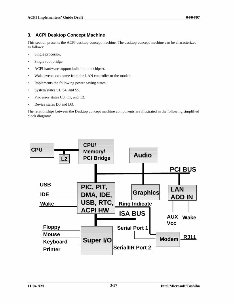
ACPI Implementers’ Guide Draft 04/04/97
11:04 AM Intel/Microsoft/Toshiba3-57
3. ACPI Desktop Concept Machine
This section presents the ACPI desktop concept machine. The desktop concept machine can be characterizedas follows:
• Single processor.
• Single root bridge.
• ACPI hardware support built into the chipset.
• Wake events can come from the LAN controller or the modem.
• Implements the following power saving states:
• System states S1, S4, and S5.
• Processor states C0, C1, and C2.
• Device states D0 and D3.
The relationships between the Desktop concept machine components are illustrated in the following simplifiedblock diagram:
CPUCPUCPU/CPU/Memory/Memory/PCI BridgePCI BridgeL2L2
PIC, PIT,PIC, PIT,DMA, IDE,DMA, IDE,USB, RTC,USB, RTC,ACPI HWACPI HW
PCI BUS
Super I/OSuper I/O
GraphicsGraphics LANLANADD INADD IN
AudioAudio
ISA BUS AUXVcc
Wake
USB
IDE
Printer
FloppyMouseKeyboard
Serial/IR Port 2
Serial Port 1
ModemModem RJ11
Ring IndicateWake
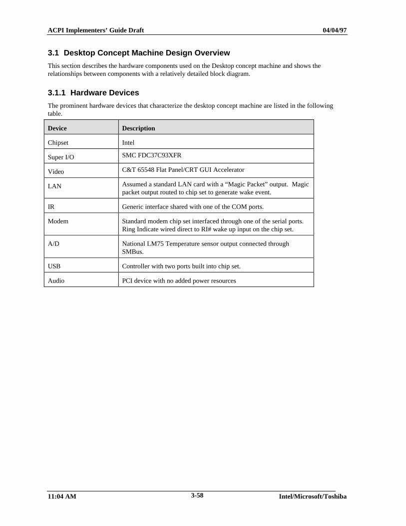
ACPI Implementers’ Guide Draft 04/04/97
11:04 AM Intel/Microsoft/Toshiba3-58
3.1 Desktop Concept Machine Design Overview
This section describes the hardware components used on the Desktop concept machine and shows therelationships between components with a relatively detailed block diagram.
3.1.1 Hardware Devices
The prominent hardware devices that characterize the desktop concept machine are listed in the followingtable.
Device Description
Chipset Intel
Super I/O SMC FDC37C93XFR
Video C&T 65548 Flat Panel/CRT GUI Accelerator
LAN Assumed a standard LAN card with a “Magic Packet” output. Magicpacket output routed to chip set to generate wake event.
IR Generic interface shared with one of the COM ports.
Modem Standard modem chip set interfaced through one of the serial ports.Ring Indicate wired direct to RI# wake up input on the chip set.
A/D National LM75 Temperature sensor output connected throughSMBus.
USB Controller with two ports built into chip set.
Audio PCI device with no added power resources
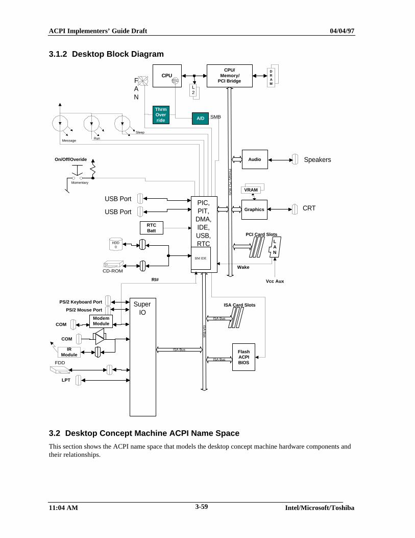
ACPI Implementers’ Guide Draft 04/04/97
11:04 AM Intel/Microsoft/Toshiba3-59
3.1.2 Desktop Block Diagram
Prim
ary PC
I BU
S
PIC,PIT,
DMA,IDE,USB,RTC
FlashACPIBIOS
SuperIO
PS/2 Keyboard Port
PS/2 Mouse Port
LPT
COM
USB Port
USB Port
BM IDE
FDD
Graphics
VRAM
CRTIS
A B
us
ISA Bus
PCI Card Slots
ISA Bus
LAN
On/Off/Overide
A/D SMB
Wake
ISA Card Slots
RTCBatt
RI#
HDD0
CD-ROM
IRModule
CPUCPU/
Memory/PCI Bridge
DRAM
L2
FAN
ISA Bus
MessageRun
Sleep
Vcc Aux
COMModemModule
ThrmOverride
Audio Speakers
Momentary
3.2 Desktop Concept Machine ACPI Name Space
This section shows the ACPI name space that models the desktop concept machine hardware components andtheir relationships.
ACPI Implementers’ Guide Draft 04/04/97
11:04 AM Intel/Microsoft/Toshiba3-60
3.2.1 Structure of the Data and Address Buses in ACPI Name Space
The backbone of ACPI name space is the hierarchy of device objects for the data and address buses, which isshown below. The desktop concept machine is a single-processor, single-root bridge machine and that showsin the diagram below.
\_PR //Single processor object...
\_SBPCI0 //Root PCI bus object
.
.
.ISA //PCI-ISA bridge object
.
.
.USB0 //USB Device objectLAN0 //LAN device object
3.2.2 All the Objects in the ACPI Name Space
This section shows all the objects in the hierarchical ACPI name space for the desktop concept machine.
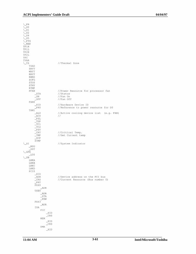
ACPI Implementers’ Guide Draft 04/04/97
11:04 AM Intel/Microsoft/Toshiba3-61
\_PR\_S0\_S1\_S2\_S4\_S5\_PTS\_WAKTP1HTP1LTP2HTP2LTPCTVAR\_TZ //Thermal Zone
TSADSBYTWBYTRBYTRWRDSCFGSTOSSTHYRTMPPFAN //Power Resource for processor fan
_STA //Status_ON //Fan On_OFF //Fan Off
FAN0_HID //Hardware Device ID_PR0 //Reference to power resource for D0
THM1_AL0 //Active cooling device list (e.g. FAN)_AC0 //_PSL_TSP_TC1_TC2_PSV_CRT //Critical Temp._TMP //Get Current temp_SCPSTMP
\_SI //System Indicator_MSG_SST
\_GPE_L00
\_SBLNKALNKBLNKCLNKDPCI0
_HID_ADR //Device address on the PCI bus_CRS //Current Resource (Bus number 0)_PRTPX40
_ADRUSB0
_ADR_STA_PRW
PX43_ADR
ISAPIC
_HID_CRS
MEM_HID_CRS
DMA_HID
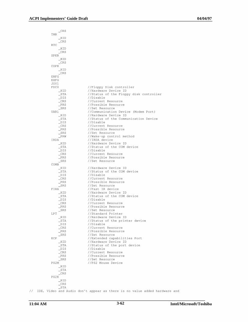
ACPI Implementers’ Guide Draft 04/04/97
11:04 AM Intel/Microsoft/Toshiba3-62
_CRSTMR
_HID_CRS
RTC_HID_CRS
SPKR_HID_CRS
COPR_HID_CRS
ENFGEXFGJOY1FDC0 //Floppy Disk controller
_HID //Hardware Device ID_STA //Status of the Floppy disk controller_DIS //Disable_CRS //Current Resource_PRS //Possible Resource_SRS //Set Resource
UAR1 //Communication Device (Modem Port)_HID //Hardware Device ID_STA //Status of the Communication Device_DIS //Disable_CRS //Current Resource_PRS //Possible Resource_SRS //Set Resource_PRW //Wake-up control method
IRDA //IRDA device_HID //Hardware Device ID_STA //Status of the COM device_DIS //Disable_CRS //Current Resource_PRS //Possible Resource_SRS //Set Resource
COMB_HID //Hardware Device ID_STA //Status of the COM device_DIS //Disable_CRS //Current Resource_PRS //Possible Resource_SRS //Set Resource
FIRA //Fast IR device_HID //Hardware Device ID_STA //Status of the COM device_DIS //Disable_CRS //Current Resource_PRS //Possible Resource_SRS //Set Resource
LPT //Standard Printer_HID //Hardware Device ID_STA //Status of the printer device_DIS //Disable_CRS //Current Resource_PRS //Possible Resource_SRS //Set Resource
ECP //Extended capabilities Port_HID //Hardware Device ID_STA //Status of the port device_DIS //Disable_CRS //Current Resource_PRS //Possible Resource_SRS //Set Resource
PS2M //PS2 Mouse Device_HID_STA_CRS
PS2K_HID_CRS_STA
// IDE, Video and Audio don’t appear as there is no value added hardware and
ACPI Implementers’ Guide Draft 04/04/97
11:04 AM Intel/Microsoft/Toshiba3-63
// system uses the standard PCI PnP and standard driver support power// management
LAN0_ADR_PRW
3.3 Implementation Examples from the Desktop Concept Machine
This section uses blocks of example ASL code, name space diagrams, and hardware component blockdiagrams to discuss in some detail the following aspects of the Desktop concept machine:
• Power resource implementation.
• Thermal zone implementation.
• Power Button support.
• Operation region and field definitions for a Super I/O chip.
3.3.1 Power Resource Implementation
The ACPI specification defines a power resource as system components (for example, power planes and clocksources) that a device requires to operate in a given power state. An example of a device on the Desktopconcept machine that operates in different power states is system fan (the device named “FAN0” in the ACPIname space). FAN0 has two power states: D0 (fully on) and D3 (fully off). The power state of the fan isswitched by writing a 0 or 1 to bit 0 of the GPOB. Following are the lines of sample ASL code that worktogether to control the system fan (the line numbers are artifacts to make it easier to walk through the code):
• Lines 3 through 6 declare a field in System I/O space named ‘FANM’ that can be read to check fan powerstatus and written to switch the fan device power states.
• Lines 8 through 19 declare the PowerResource object named ‘PFAN’ for the fan device (declared as‘FAN0’ in lines 20 through 23). Typically, a PowerResource object contains methods for device power(Dx) states and for determining the current power state of the device. Notice that in the ‘PFAN’PowerResource object, the ‘FANM’ field is used to switch the fan between D0 (fully on) and D3 (fully off)and to determine the status.
• Line 22 links the device named ‘FAN0’ to the PowerResource named ‘PFAN’.
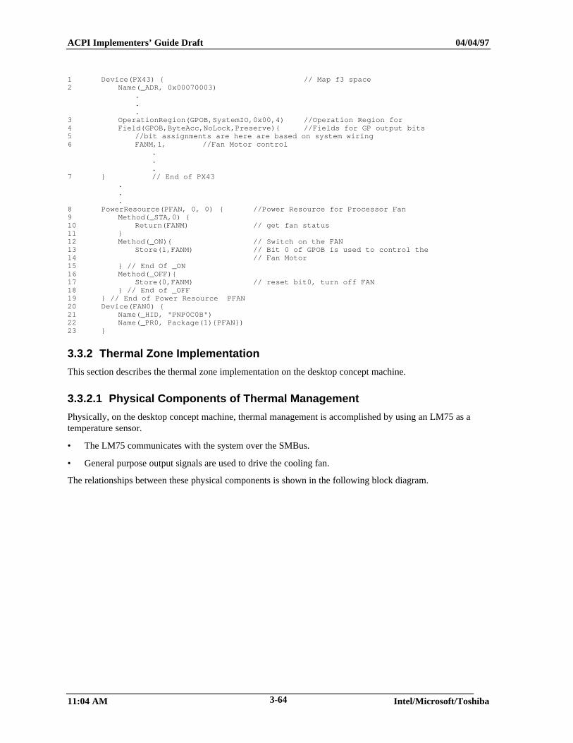
ACPI Implementers’ Guide Draft 04/04/97
11:04 AM Intel/Microsoft/Toshiba3-64
1 Device(PX43) { // Map f3 space2 Name(_ADR, 0x00070003)
.
.
.3 OperationRegion(GPOB,SystemIO,0x00,4) //Operation Region for4 Field(GPOB,ByteAcc,NoLock,Preserve){ //Fields for GP output bits5 //bit assignments are here are based on system wiring6 FANM,1, //Fan Motor control
.
.
.7 } // End of PX43
.
.
.8 PowerResource(PFAN, 0, 0) { //Power Resource for Processor Fan9 Method(_STA,0) {10 Return(FANM) // get fan status11 }12 Method(_ON){ // Switch on the FAN13 Store(1,FANM) // Bit 0 of GPOB is used to control the14 // Fan Motor15 } // End Of _ON16 Method(_OFF){17 Store(0,FANM) // reset bit0, turn off FAN18 } // End of _OFF19 } // End of Power Resource PFAN20 Device(FAN0) {21 Name(_HID, "PNP0C0B")22 Name(_PR0, Package(1){PFAN})23 }
3.3.2 Thermal Zone Implementation
This section describes the thermal zone implementation on the desktop concept machine.
3.3.2.1 Physical Components of Thermal Management
Physically, on the desktop concept machine, thermal management is accomplished by using an LM75 as atemperature sensor.
• The LM75 communicates with the system over the SMBus.
• General purpose output signals are used to drive the cooling fan.
The relationships between these physical components is shown in the following block diagram.
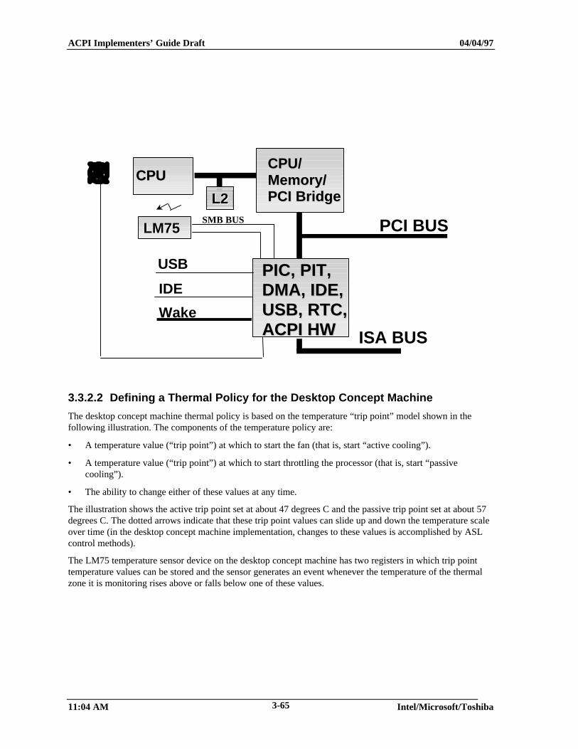
ACPI Implementers’ Guide Draft 04/04/97
11:04 AM Intel/Microsoft/Toshiba3-65
CPUCPUCPU/CPU/Memory/Memory/PCI BridgePCI BridgeL2L2
PIC, PIT,PIC, PIT,DMA, IDE,DMA, IDE,USB, RTC,USB, RTC,ACPI HWACPI HW
PCI BUS
ISA BUS
USB
IDE
Wake
LM75LM75SMB BUS
3.3.2.2 Defining a Thermal Policy for the Desktop Concept Machine
The desktop concept machine thermal policy is based on the temperature “trip point” model shown in thefollowing illustration. The components of the temperature policy are:
• A temperature value (“trip point”) at which to start the fan (that is, start “active cooling”).
• A temperature value (“trip point”) at which to start throttling the processor (that is, start “passivecooling”).
• The ability to change either of these values at any time.
The illustration shows the active trip point set at about 47 degrees C and the passive trip point set at about 57degrees C. The dotted arrows indicate that these trip point values can slide up and down the temperature scaleover time (in the desktop concept machine implementation, changes to these values is accomplished by ASLcontrol methods).
The LM75 temperature sensor device on the desktop concept machine has two registers in which trip pointtemperature values can be stored and the sensor generates an event whenever the temperature of the thermalzone it is monitoring rises above or falls below one of these values.
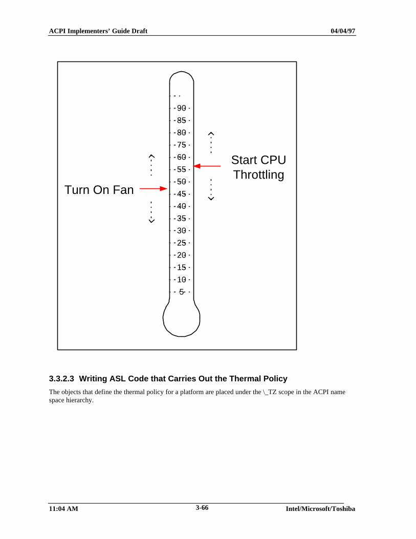
ACPI Implementers’ Guide Draft 04/04/97
11:04 AM Intel/Microsoft/Toshiba3-66
Turn On Fan
5
10
15
20
25
30
35
40
45
50
55
60
75
80
85
90
Start CPUThrottling
3.3.2.3 Writing ASL Code that Carries Out the Thermal Policy
The objects that define the thermal policy for a platform are placed under the \_TZ scope in the ACPI namespace hierarchy.
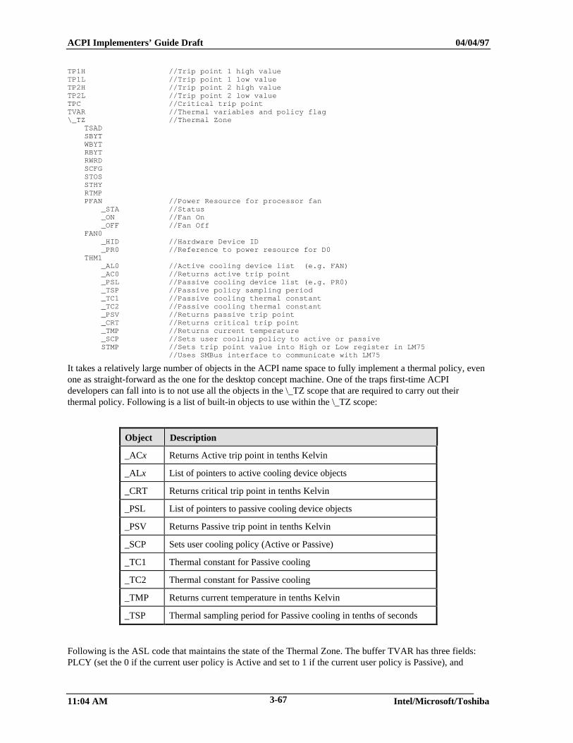
ACPI Implementers’ Guide Draft 04/04/97
11:04 AM Intel/Microsoft/Toshiba3-67
TP1H //Trip point 1 high valueTP1L //Trip point 1 low valueTP2H //Trip point 2 high valueTP2L //Trip point 2 low valueTPC //Critical trip pointTVAR //Thermal variables and policy flag\_TZ //Thermal Zone
TSADSBYTWBYTRBYTRWRDSCFGSTOSSTHYRTMPPFAN //Power Resource for processor fan
_STA //Status_ON //Fan On_OFF //Fan Off
FAN0_HID //Hardware Device ID_PR0 //Reference to power resource for D0
THM1_AL0 //Active cooling device list (e.g. FAN)_AC0 //Returns active trip point_PSL //Passive cooling device list (e.g. PR0)_TSP //Passive policy sampling period_TC1 //Passive cooling thermal constant_TC2 //Passive cooling thermal constant_PSV //Returns passive trip point_CRT //Returns critical trip point_TMP //Returns current temperature_SCP //Sets user cooling policy to active or passiveSTMP //Sets trip point value into High or Low register in LM75
//Uses SMBus interface to communicate with LM75
It takes a relatively large number of objects in the ACPI name space to fully implement a thermal policy, evenone as straight-forward as the one for the desktop concept machine. One of the traps first-time ACPIdevelopers can fall into is to not use all the objects in the \_TZ scope that are required to carry out theirthermal policy. Following is a list of built-in objects to use within the \_TZ scope:
Object Description
_ACx Returns Active trip point in tenths Kelvin
_ALx List of pointers to active cooling device objects
_CRT Returns critical trip point in tenths Kelvin
_PSL List of pointers to passive cooling device objects
_PSV Returns Passive trip point in tenths Kelvin
_SCP Sets user cooling policy (Active or Passive)
_TC1 Thermal constant for Passive cooling
_TC2 Thermal constant for Passive cooling
_TMP Returns current temperature in tenths Kelvin
_TSP Thermal sampling period for Passive cooling in tenths of seconds
Following is the ASL code that maintains the state of the Thermal Zone. The buffer TVAR has three fields:PLCY (set the 0 if the current user policy is Active and set to 1 if the current user policy is Passive), and
ACPI Implementers’ Guide Draft 04/04/97
11:04 AM Intel/Microsoft/Toshiba3-68
CTOS and CTHY (which hold the values for the two LM75 registers). Note the ASL coding technique of theASL CreateByteField and CreateWordField terms to create named fields (substrings) out of a string in aBuffer.
//// Thermal Zones// Define thermal constants, flag and variablesName(TP1H, 3332) // Trip point 1 high = 60.0cName(TP1L, 3282) // Trip point 1 low = 55.0cName(TP2H, 3432) // Trip point 2 high = 70.0cName(TP2L, 3382) // Trip point 2 low = 65.0cName(TPC, 3532) // Critical trip point = 80.0cName(TVAR, Buffer(){1, 32, 33, 82, 32}) // Thermal variables and flagCreateByteField(TVAR, 0, PLCY) // Default policy to passiveCreateWordField(TVAR, 1, CTOS) // Current Tos = 40.0cCreateWordField(TVAR, 3, CTHY) // Current Thyst = 35.0c
The ASL code that implements the thermal policy for the Desktop concept machine is shown below (linenumbers are artifacts to make it easier to refer to particular lines of code).
Lines 56 through 64 is a control method that sets one of the trip point registers in the LM75. This method,named ‘STMP’, takes two arguments: which trip point register to set in the LM75 (high or low); thetemperature value to put into the register. The STMP method uses the STOS or STHY method to move thenew value into the appropriate LM75 register (the ASL code for the STOS and STHY methods is shown in alater section; an SMBus interface is used by these methods to communicate with the LM75 and that is beyondthe scope of this discussion).
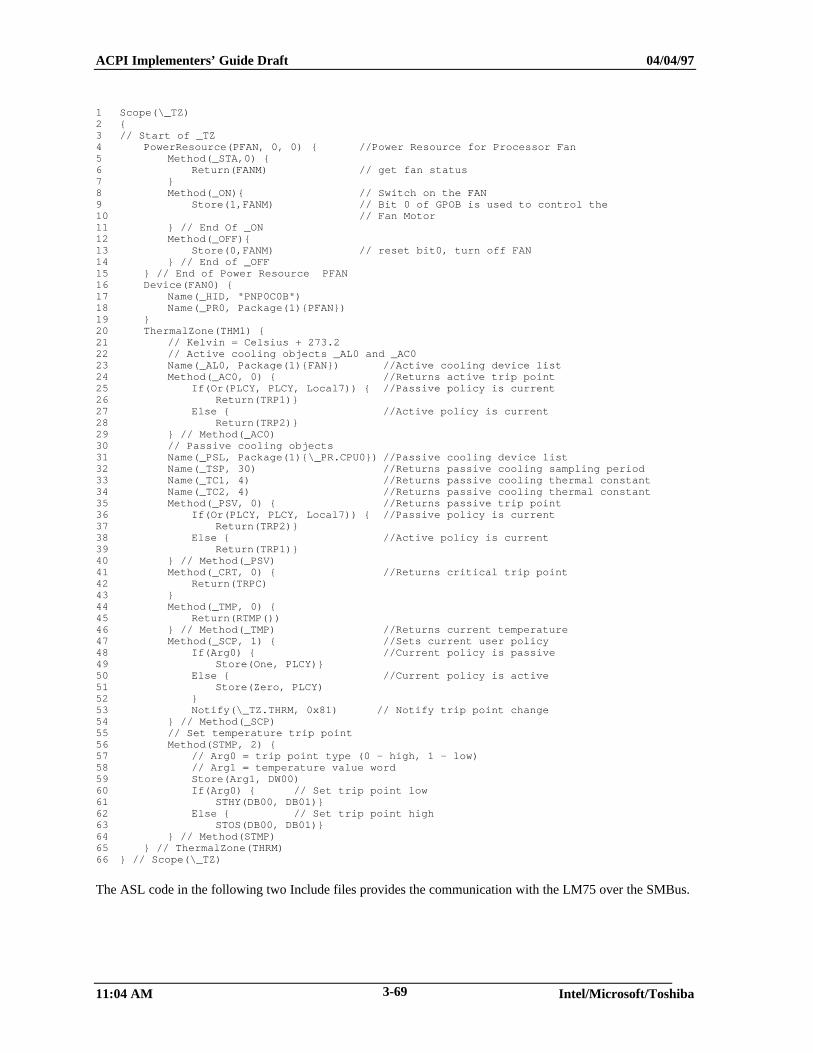
ACPI Implementers’ Guide Draft 04/04/97
11:04 AM Intel/Microsoft/Toshiba3-69
1 Scope(\_TZ)2 {3 // Start of _TZ4 PowerResource(PFAN, 0, 0) { //Power Resource for Processor Fan5 Method(_STA,0) {6 Return(FANM) // get fan status7 }8 Method(_ON){ // Switch on the FAN9 Store(1,FANM) // Bit 0 of GPOB is used to control the10 // Fan Motor11 } // End Of _ON12 Method(_OFF){13 Store(0,FANM) // reset bit0, turn off FAN14 } // End of _OFF15 } // End of Power Resource PFAN16 Device(FAN0) {17 Name(_HID, "PNP0C0B")18 Name(_PR0, Package(1){PFAN})19 }20 ThermalZone(THM1) {21 // Kelvin = Celsius + 273.222 // Active cooling objects _AL0 and _AC023 Name(_AL0, Package(1){FAN}) //Active cooling device list24 Method(_AC0, 0) { //Returns active trip point25 If(Or(PLCY, PLCY, Local7)) { //Passive policy is current26 Return(TRP1)}27 Else { //Active policy is current28 Return(TRP2)}29 } // Method(_AC0)30 // Passive cooling objects31 Name(_PSL, Package(1){\_PR.CPU0}) //Passive cooling device list32 Name(_TSP, 30) //Returns passive cooling sampling period33 Name(_TC1, 4) //Returns passive cooling thermal constant34 Name(_TC2, 4) //Returns passive cooling thermal constant35 Method(_PSV, 0) { //Returns passive trip point36 If(Or(PLCY, PLCY, Local7)) { //Passive policy is current37 Return(TRP2)}38 Else { //Active policy is current39 Return(TRP1)}40 } // Method(_PSV)41 Method(_CRT, 0) { //Returns critical trip point42 Return(TRPC)43 }44 Method(_TMP, 0) {45 Return(RTMP())46 } // Method(_TMP) //Returns current temperature47 Method(_SCP, 1) { //Sets current user policy48 If(Arg0) { //Current policy is passive49 Store(One, PLCY)}50 Else { //Current policy is active51 Store(Zero, PLCY)52 }53 Notify(\_TZ.THRM, 0x81) // Notify trip point change54 } // Method(_SCP)55 // Set temperature trip point56 Method(STMP, 2) {57 // Arg0 = trip point type (0 - high, 1 - low)58 // Arg1 = temperature value word59 Store(Arg1, DW00)60 If(Arg0) { // Set trip point low61 STHY(DB00, DB01)}62 Else { // Set trip point high63 STOS(DB00, DB01)}64 } // Method(STMP)65 } // ThermalZone(THRM)66 } // Scope(\_TZ)
The ASL code in the following two Include files provides the communication with the LM75 over the SMBus.

ACPI Implementers’ Guide Draft 04/04/97
11:04 AM Intel/Microsoft/Toshiba3-70
3.3.2.3.1 LM75 Thermal Device Include File
This section shows the contents of the Include file Lm75.asl.
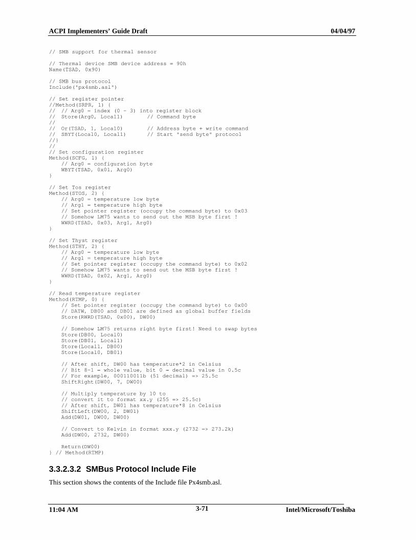
ACPI Implementers’ Guide Draft 04/04/97
11:04 AM Intel/Microsoft/Toshiba3-71
// SMB support for thermal sensor
// Thermal device SMB device address = 90hName(TSAD, 0x90)
// SMB bus protocolInclude("px4smb.asl")
// Set register pointer//Method(SRPR, 1) {// // Arg0 = index (0 - 3) into register block// Store(Arg0, Local1) // Command byte//// Or(TSAD, 1, Local0) // Address byte + write command// SBYT(Local0, Local1) // Start "send byte" protocol//}//// Set configuration registerMethod(SCFG, 1) {
// Arg0 = configuration byteWBYT(TSAD, 0x01, Arg0)
}
// Set Tos registerMethod(STOS, 2) {
// Arg0 = temperature low byte// Arg1 = temperature high byte// Set pointer register (occupy the command byte) to 0x03// Somehow LM75 wants to send out the MSB byte first !WWRD(TSAD, 0x03, Arg1, Arg0)
}
// Set Thyst registerMethod(STHY, 2) {
// Arg0 = temperature low byte// Arg1 = temperature high byte// Set pointer register (occupy the command byte) to 0x02// Somehow LM75 wants to send out the MSB byte first !WWRD(TSAD, 0x02, Arg1, Arg0)
}
// Read temperature registerMethod(RTMP, 0) {
// Set pointer register (occupy the command byte) to 0x00// DATW, DB00 and DB01 are defined as global buffer fieldsStore(RWRD(TSAD, 0x00), DW00)
// Somehow LM75 returns right byte first! Need to swap bytesStore(DB00, Local0)Store(DB01, Local1)Store(Local1, DB00)Store(Local0, DB01)
// After shift, DW00 has temperature*2 in Celsius// Bit 8-1 = whole value, bit 0 = decimal value in 0.5c// For example, 000110011b (51 decimal) => 25.5cShiftRight(DW00, 7, DW00)
// Multiply temperature by 10 to// convert it to format xx.y (255 => 25.5c)// After shift, DW01 has temperature*8 in CelsiusShiftLeft(DW00, 2, DW01)Add(DW01, DW00, DW00)
// Convert to Kelvin in format xxx.y (2732 => 273.2k)Add(DW00, 2732, DW00)
Return(DW00)} // Method(RTMP)
3.3.2.3.2 SMBus Protocol Include File
This section shows the contents of the Include file Px4smb.asl.
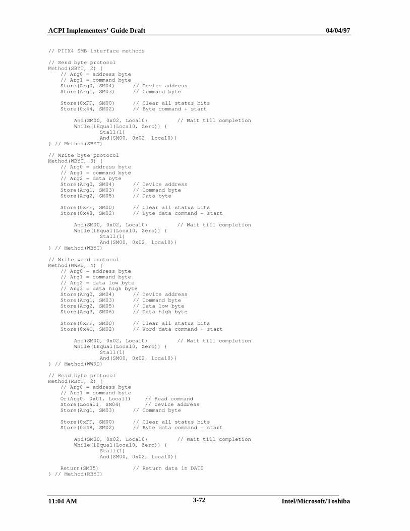
ACPI Implementers’ Guide Draft 04/04/97
11:04 AM Intel/Microsoft/Toshiba3-72
// PIIX4 SMB interface methods
// Send byte protocolMethod(SBYT, 2) {
// Arg0 = address byte// Arg1 = command byteStore(Arg0, SM04) // Device addressStore(Arg1, SM03) // Command byte
Store(0xFF, SM00) // Clear all status bitsStore(0x44, SM02) // Byte command + start
And(SM00, 0x02, Local0) // Wait till completion While(LEqual(Local0, Zero)) { Stall(1) And(SM00, 0x02, Local0)}} // Method(SBYT)
// Write byte protocolMethod(WBYT, 3) {
// Arg0 = address byte// Arg1 = command byte// Arg2 = data byteStore(Arg0, SM04) // Device addressStore(Arg1, SM03) // Command byteStore(Arg2, SM05) // Data byte
Store(0xFF, SM00) // Clear all status bitsStore(0x48, SM02) // Byte data command + start
And(SM00, 0x02, Local0) // Wait till completion While(LEqual(Local0, Zero)) { Stall(1) And(SM00, 0x02, Local0)}} // Method(WBYT)
// Write word protocolMethod(WWRD, 4) {
// Arg0 = address byte// Arg1 = command byte// Arg2 = data low byte// Arg3 = data high byteStore(Arg0, SM04) // Device addressStore(Arg1, SM03) // Command byteStore(Arg2, SM05) // Data low byteStore(Arg3, SM06) // Data high byte
Store(0xFF, SM00) // Clear all status bitsStore(0x4C, SM02) // Word data command + start
And(SM00, 0x02, Local0) // Wait till completion While(LEqual(Local0, Zero)) { Stall(1) And(SM00, 0x02, Local0)}} // Method(WWRD)
// Read byte protocolMethod(RBYT, 2) {
// Arg0 = address byte// Arg1 = command byteOr(Arg0, 0x01, Local1) // Read commandStore(Local1, SM04) // Device addressStore(Arg1, SM03) // Command byte
Store(0xFF, SM00) // Clear all status bitsStore(0x48, SM02) // Byte data command + start
And(SM00, 0x02, Local0) // Wait till completion While(LEqual(Local0, Zero)) { Stall(1) And(SM00, 0x02, Local0)}
Return(SM05) // Return data in DAT0} // Method(RBYT)
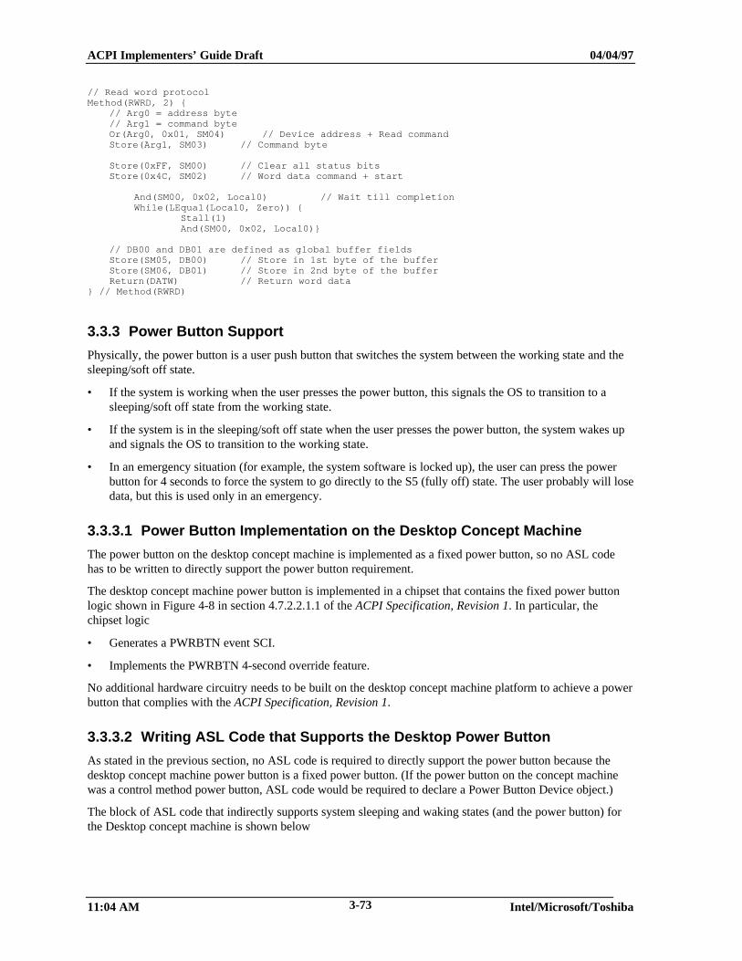
ACPI Implementers’ Guide Draft 04/04/97
11:04 AM Intel/Microsoft/Toshiba3-73
// Read word protocolMethod(RWRD, 2) {
// Arg0 = address byte// Arg1 = command byteOr(Arg0, 0x01, SM04) // Device address + Read commandStore(Arg1, SM03) // Command byte
Store(0xFF, SM00) // Clear all status bitsStore(0x4C, SM02) // Word data command + start
And(SM00, 0x02, Local0) // Wait till completion While(LEqual(Local0, Zero)) { Stall(1) And(SM00, 0x02, Local0)}
// DB00 and DB01 are defined as global buffer fieldsStore(SM05, DB00) // Store in 1st byte of the bufferStore(SM06, DB01) // Store in 2nd byte of the bufferReturn(DATW) // Return word data
} // Method(RWRD)
3.3.3 Power Button Support
Physically, the power button is a user push button that switches the system between the working state and thesleeping/soft off state.
• If the system is working when the user presses the power button, this signals the OS to transition to asleeping/soft off state from the working state.
• If the system is in the sleeping/soft off state when the user presses the power button, the system wakes upand signals the OS to transition to the working state.
• In an emergency situation (for example, the system software is locked up), the user can press the powerbutton for 4 seconds to force the system to go directly to the S5 (fully off) state. The user probably will losedata, but this is used only in an emergency.
3.3.3.1 Power Button Implementation on the Desktop Concept Machine
The power button on the desktop concept machine is implemented as a fixed power button, so no ASL codehas to be written to directly support the power button requirement.
The desktop concept machine power button is implemented in a chipset that contains the fixed power buttonlogic shown in Figure 4-8 in section 4.7.2.2.1.1 of the ACPI Specification, Revision 1. In particular, thechipset logic
• Generates a PWRBTN event SCI.
• Implements the PWRBTN 4-second override feature.
No additional hardware circuitry needs to be built on the desktop concept machine platform to achieve a powerbutton that complies with the ACPI Specification, Revision 1.
3.3.3.2 Writing ASL Code that Supports the Desktop Power Button
As stated in the previous section, no ASL code is required to directly support the power button because thedesktop concept machine power button is a fixed power button. (If the power button on the concept machinewas a control method power button, ASL code would be required to declare a Power Button Device object.)
The block of ASL code that indirectly supports system sleeping and waking states (and the power button) forthe Desktop concept machine is shown below
ACPI Implementers’ Guide Draft 04/04/97
11:04 AM Intel/Microsoft/Toshiba3-74
Name(\_S0,Package(2){5,5}) // Value to be set in SLP_TYP register (S0)working state// on this chip set
Name(\_S1,Package(2){4,4}) // Value to be set in SLP_TYP register for S1 state// on this chip set
Name(\_S2,Package(2){3,3}) // Power on suspend with CPU context lost.Name(\_S4,Package(2){Zero,Zero}) // Value to be set in SLP_TYP register for Soft Off
// on this chip setName(\_S5,Package(2){Zero,Zero}) // Value to be set in SLP_TYP register for Soft Off
// on this chip set////Method(\_PTS) { //prepare to sleep(Not used in this implementation)// }Method(\WAK,1){
Notify(THM1,0x80)}
3.3.4 Operation Region and Field Definitions for a Super I/O Chip
The SMC Super I/O chip registers are read and written through a level of indirection. A working register isaccessed by designating a particular register in an 8-bit Index register and reading or writing the workingregister through an 8-bit Data register. The ASL language OperationRegion, Field, and IndexField termscan be declared in combination to define this two-tier register arrangement, assigning field names to theworking registers of interest. Once this declaration is made, simple Store terms can be used to read from andwrite to the field names and the ACPI run-time component built into the OS automatically takes care of all thedetails of managing the Index and Data registers.
For example, the block of ASL code that declares field names for Super I/O chip working registers is shownbelow (line numbers are artifacts to make it easier to refer to particular lines of code).
ACPI Implementers’ Guide Draft 04/04/97
11:04 AM Intel/Microsoft/Toshiba3-75
1 // Start of Definitions for SMC super I/O device2 OperationRegion(SMC1, // name of Operation Region for SuperIO device3 SystemIO, // type of address space4 0x3F0, // offset to start of region5 // (default offset for SuperIO device)6 // (Real systems will likely have BIOS relocate this device7 // to avoid conflicts with secondary floppy ID of 0x370)8 2) //size of region in bytes9 //end of Operation Region10 Field ( SMC1, //fields are in Operation Region named SMC111 ByteAcc,12 NoLock,13 Preserve)14 {15 INDX,8, //field named INDX is 8 bits wide16 DATA,8 //field named DATA is 8 bits wide17 }18 IndexField(INDX, //index name19 DATA, //name of I/O port20 ByteAcc,21 NoLock,22 Preserve)23 {24 Offset(2),25 CFG,8, //global config control register26 Offset(7),27 LDN,8, //Logical Device Number, offset 0x0728 Offset(0x30),29 ACTR,8, //activate register, offset 0x3030 Offset(0x60),31 IOAH,8, //base I/O addr, offset 0x6032 IOAL,8,33 Offset(0x70),34 INTR,8, //IRQ, Offset 0x7035 Offset(0x72),36 INT1,8, //Second IRQ for some devices, Offset 0x7237 Offset(0x74),38 DMCH,8, //DMA channel, offset 0x7439 Offset(0xC0),40 GP40,8, //Fast IR control bits, Offset(0xC0)41 Offset(0xF0),42 OPT1,8, //Option register 1, Offset(0xF0)43 OPT2,8, //Option register 244 OPT3,8 //Option register 345 } //end of indexed field46 Method(ENFG,0){ // Enter Config Mode for SMC47 Store(0x55,INDX)48 Store(0x55,INDX)49 } // end ENFG method50 Method(EXFG,0){ // Exit Config Mode for SMC51 Store(0xAA,INDX)52 } // end EXFG method
3.4 Desktop Sample ASL Code
The following ASL code implements the ACPI name space for the desktop concept machine. Notice that theASL code has been broken into sections using the ASL compiler Include directive. The following sections ofdesktop concept machine sample code is organized in the same way.
ACPI Implementers’ Guide Draft 04/04/97
11:04 AM Intel/Microsoft/Toshiba3-76
3.4.1 Main File of Desktop Concept Machine Sample Code
DefinitionBlock ("DT_1.AML","DSDT",0x01,"OEMx","DT_1",0x1002)
{ // Start of ASL File// Processor ObjectsScope(\_PR) {
Processor( CPU0,1, //processor number0xFFD0, //System IO address of Pblk Registers0x06 //length in bytes of PBlk) {}
} // end Scope _PRName(\_S0,Package(2){5,5}) // Value to be set in SLP_TYP register (S0)working state
// on this chip setName(\_S1,Package(2){4,4}) // Value to be set in SLP_TYP register for S1 state
// on this chip setName(\_S2,Package(2){3,3}) // Power on suspend with CPU context lost.Name(\_S4,Package(2){Zero,Zero}) // Value to be set in SLP_TYP register for Soft Off
// on this chip setName(\_S5,Package(2){Zero,Zero}) // Value to be set in SLP_TYP register for Soft Off
// on this chip set////Method(\_PTS) { //prepare to sleep(Not used in this implementation)// }Method(\WAK,1){
Notify(THM1,0x80)}//// Thermal Zones// Define thermal constants, flag and variablesName(TP1H, 3332) // Trip point 1 high = 60.0cName(TP1L, 3282) // Trip point 1 low = 55.0cName(TP2H, 3432) // Trip point 2 high = 70.0cName(TP2L, 3382) // Trip point 2 low = 65.0cName(TPC, 3532) // Critical trip point = 80.0cName(TVAR, buffer(){1, 32, 33, 82, 32}) // Thermal variables and flagCreateByteField(TVAR, 0, PLCY) // Default policy to passiveCreateWordField(TVAR, 1, CTOS) // Current Tos = 40.0cCreateWordField(TVAR, 3, CTHY) // Current Thyst = 35.0c
Scope(\_TZ){Include ("lm75.asl")// Start of _TZ
PowerResource(PFAN, 0, 0) { //Power Resource for Processor FanMethod(_STA,0) {
Return(FANM) // get fan status}
Method(_ON){ // Switch on the FANStore(1,FANM) // Bit 0 of GPOB is used to control the
// Fan Motor} // End Of _ON
Method(_OFF){Store(0,FANM) // reset bit0, turn off FAN
} // End of _OFF
} // End of Power Resource PFAN
Device(FAN0) {Name(_HID, "PNP0C0B")Name(_PR0, Package(1){PFAN})
}
ACPI Implementers’ Guide Draft 04/04/97
11:04 AM Intel/Microsoft/Toshiba3-77
ThermalZone(THM1) {// Kelvin = Celsius + 273.2// Active coolingName(_AL0, Package(1){FAN})Method(_AC0, 0) {
If(Or(PLCY, PLCY, Local7)) { // Passive policyReturn(TRP1)}
Else { // Active policyReturn(TRP2)}
} // Method(_AC0)
// Passive coolingName(_PSL, Package(1){\_PR.CPU0})Name(_TSP, 30) // Sampling periodName(_TC1, 4)Name(_TC2, 4)Method(_PSV, 0) {
If(Or(PLCY, PLCY, Local7)) { // Passive policyReturn(TRP2)}
Else { // Active policyReturn(TRP1)}
} // Method(_PSV)
Method(_CRT, 0) {Return(TRPC)}
Method(_TMP, 0) {Return(RTMP())
} // Method(_TMP)
Method(_SCP, 1) {If(Arg0) { // Passive policy
Store(One, PLCY)}Else { // Active policy
Store(Zero, PLCY)}
Notify(\_TZ.THRM, 0x81) // Notify trip point change} // Method(_SCP)
// Set temperature trip pointMethod(STMP, 2) {
// Arg0 = trip point type (0 - high, 1 - low)// Arg1 = temperature value wordStore(Arg1, DW00)If(Arg0) { // Set trip point low
STHY(DB00, DB01)}Else { // Set trip point high
STOS(DB00, DB01)}} // Method(STMP)
} // ThermalZone(THRM)} // Scope(\_TZ)
//// System Indicators//Scope(\_SI){ // Start of _SI
Method(_MSG, 1){If (LEqual(ARG0,Zero))
{Store(Zero, MSG)} //Turn message light off if no messagesElse
{Store(One, MSG)} //Turn message light on if any messages} // End of MethodMethod(_SST, 1) {
If (LEqual(Arg0,Zero)) {Store(Zero,IND0) //Turn both status indicators offStore(Zero,IND1)Return(0)}
If (LEqual(Arg0,One)) {Store(One,IND0) //Turn on both indicators for working stateStore(One,IND1)Return(0)}
If (LEqual(Arg0,2)) {Store(Zero,IND0) //Turn on IND1 indicator for s1, s2 or s3 state
ACPI Implementers’ Guide Draft 04/04/97
11:04 AM Intel/Microsoft/Toshiba3-78
Store(One,IND1)Return(0)}
If (LEqual(Arg0,3)) {Store(One,IND0) //Turn on IND0 indicators for working stateStore(Zero,IND1)Return(0)}
If (LEqual(Arg0,4)) {Store(Zero,IND0) //Turn both indicators off for non-volatile sleepStore(Zero,IND1)Return(0)}
} // End of Method} // End of _SI//// General Purpose Event Handlers//Scope(\_GPE){
Method (_L00){ //GP event for thermalNotify(THM1,0)
}} //end GPE//// System Bus//Scope(\_SB) { // Start of _SB
Device(LNKA){Name(_HID, EISAID("PNP0C0F")) // PCI interrupt linkName(_UID, 1)
// Name(_PRS, ResourceTemplate(){// Interrupt(ResourceProducer,...) {10,11} // IRQs 10,11// })// Method(_DIS) {...}// Method(_CRS) {...}// Method(_SRS, 1) {...}
}Device(LNKB){
Name(_HID, EISAID("PNP0C0F")) // PCI interrupt linkName(_UID, 2)
// Name(_PRS, ResourceTemplate(){// Interrupt(ResourceProducer,...) {11,12} // IRQs 11,12// })// Method(_DIS) {...}// Method(_CRS) {...}// Method(_SRS, 1) {...}
}Device(LNKC){
Name(_HID, EISAID("PNP0C0F")) // PCI interrupt linkName(_UID, 3)
// Name(_PRS, ResourceTemplate(){// Interrupt(ResourceProducer,...) {12,13} // IRQs 12,13// })// Method(_DIS) {...}// Method(_CRS) {...}// Method(_SRS, 1) {...}
}Device(LNKD){
Name(_HID, EISAID("PNP0C0F")) // PCI interrupt linkName(_UID, 4)
// Name(_PRS, ResourceTemplate(){// Interrupt(ResourceProducer,...) {13,14} // IRQs 13,14// })// Method(_DIS) {...}// Method(_CRS) {...}// Method(_SRS, 1) {...}
}
Device(PCI0) { // Root PCI BusName(_HID, EISAID("PNP0A03")) // Need _HID for root deviceName(_ADR,0x00000000) // Also need _ADR since this appears
// in PCI config space// Dword constant with upper word=device number// lowerword = function
Name (_CRS,0)
Name(_PRT, Package(){
ACPI Implementers’ Guide Draft 04/04/97
11:04 AM Intel/Microsoft/Toshiba3-79
Package(){0x0004ffff, 0, LNKA, 0}, // Slot 1, INTAPackage(){0x0004ffff, 1, LNKB, 0}, // Slot 1, INTBPackage(){0x0004ffff, 2, LNKC, 0}, // Slot 1, INTCPackage(){0x0004ffff, 3, LNKD, 0}, // Slot 1, INTDPackage(){0x0005ffff, 0, LNKB, 0}, // Slot 2, INTAPackage(){0x0005ffff, 1, LNKC, 0}, // Slot 2, INTBPackage(){0x0005ffff, 2, LNKD, 0}, // Slot 2, INTCPackage(){0x0006ffff, 3, LNKA, 0}, // Slot 2, INTDPackage(){0x0006ffff, 0, LNKC, 0}, // Slot 3, INTAPackage(){0x0006ffff, 1, LNKD, 0}, // Slot 3, INTBPackage(){0x0006ffff, 2, LNKA, 0}, // Slot 3, INTCPackage(){0x0006ffff, 3, LNKB, 0}, // Slot 3, INTD
})}
// not end of PCI0Device(PX40) { // Map f0 space, Start PX40
Name(_ADR,0x00070000) // Address+function. Address is defined by// how chip is connected to PCI bus
}// End of PX40
// IDE doesn't appear as there is no value added hardware and system// uses the standard PCI PnP and standard driver support power management
Device(USB0) { // Map f2 space, USB Host controllerName(_ADR, 0x00070002)// PCI Config Space Length 256 BytesOperationRegion(CFG2, PCI_Config, 0x0, 0x100)Field(CFG2,DWordAcc,NoLock,Preserve){
,32,// Word Length : AddressUSBB,16} //USB Base address
Method(_STA,0) { //Status of the USB deviceAnd(USBB,0xFFE0,Local0) //get the device base addressIf(LEqual(Local0,Zero)) //Return device present if no
{Return(One)} //Base address programmedElse
{Return(0x3)} //else return present and active} //end MethodName(_PRW,8) //Enable USB resume event
} //end of USB devices
Device(PX43) { // Map f3 spaceName(_ADR, 0x00070003)//Operation Region for Fields for GP output bitsOperationRegion(GPOB,SystemIO,0x00,4) //Note: Change “0x00” in Operation
//Region fixed list to match the//SystemIO address of your hardware!!!
Field(GPOB,ByteAcc,NoLock,Preserve){ //Fields for GP output bits//
//bit assignments are here are based on system wiringFANM,1, //Fan Motor control,23, //skipsIND0,1, //GPO[25:24] control machine status indicatorsIND1,1,,4, //skipsMSG0,1 //GPO[30] controls message light
} // End of PX43
//------------------------------ ISA ---------------------------------------//Device(ISA){ // Start of ISA
Include("memory.asl")Include("intr.asl")Include("dma.asl")Include("timer.asl")Include("rtc.asl")Include("spkr.asl")Include("coproc.asl")// SMC Code is included Under DEVICE ISAInclude("smc93xfr.asl") // Pcode for SMC super IO
} // End of ISA
Device(LAN0){ //LAN deviceName(_ADR, 0x00080000)//Device address on the PCI bus
ACPI Implementers’ Guide Draft 04/04/97
11:04 AM Intel/Microsoft/Toshiba3-80
//DWORD Upper word is device//Lower word is function
Name(_PRW, Package(2) {11, \_S4}) //Wake-up. } //end of LAN0 device
} // End of PCI 0 Bus} // End of _SB}}
3.4.2 Super IO ASL Include File
This section shows the contents of the Include file with the filename Smc93xfr.asl. Note that the followingASL code is an example only, for illustrative purposes.
ACPI Implementers’ Guide Draft 04/04/97
11:04 AM Intel/Microsoft/Toshiba3-81
// Start of Definitions for SMC super I/O deviceOperationRegion(SMC1, // name of Operation Region for SuperIO device
SystemIO, // type of address space0x3F0, // offset to start of region
// (default offset for SuperIO device)// (Real systems will likely have the BIOS relocate this device// to avoid conflicts with secondary floppy ID of 0x370)
2) //size of region in bytes//end of Operation RegionField ( SMC1, //fields are in Operation Region named SMC1
ByteAcc,NoLock,Preserve){
INDX,8, //field named INDX is b bits wideDATA,8 //field DATA is 8 bits wide
}IndexField(INDX, //index name
DATA, //name of I/O portByteAcc,NoLock,Preserve){
Offset(2),CFG,8, //global config control regOffset(7),LDN,8, //Logical Device Number, offset 0x07Offset(0x30),ACTR,8, //activate register, offset 0x30Offset(0x60),IOAH,8, //base I/O addr, offset 0x60IOAL,8,Offset(0x70),INTR,8, //IRQ, Offset 0x70Offset(0x72),INT1,8, //Second IRQ for some devices, Offset 0x72Offset(0x74),DMCH,8, //DMA channel, offset 0x74Offset(0xC0),GP40,8, //Fast IR control bits, Offset(0xC0)Offset(0xF0),OPT1,8, //Option register 1, Offset(0xF0)OPT2,8, //Option register 2OPT3,8 //Option register 3
} //end of indexed fieldMethod(ENFG,0){ // Enter Config Mode for SMC
Store(0x55,INDX)Store(0x55,INDX)
} // end ENFG methodMethod(EXFG,0){ // Exit Config Mode for SMC
Store(0xAA,INDX)} // end EXFG methodInclude("smc_FDC.asl")Include("smc_UAR1.asl")Include("smc_UAR2.asl")Include("smc_PRT.asl")Include("smc_PS2.asl")
Device(JOY1){} //end of JOY1 device
// End of SMC device
3.4.3 FDC ASL Include File
This section shows the contents of the Include file with the filename Smc_fdc.asl. Note that the following ASLcode is an example only, for illustrative purposes.
ACPI Implementers’ Guide Draft 04/04/97
11:04 AM Intel/Microsoft/Toshiba3-82
Device(FDC0) { // Floppy Disk controllerName(_HID, EISAID("PNP0700")) // PnP Device IDMethod(_STA,0){ //Status of the Floppy disk controller
//set logical device number for FloppyENFG() // Enter Config ModeStore(Zero,LDN)// is the device functioning?// read Activate Register// Return Device Present and device ActiveIf(ACTR)
{Return(3)}Else
{If (LOr(IOAH,IOAL)) {Return(One)} // If device address is non zero// return device present, not active
Else{Return(0)}} // If device address is 0
// return device not presentEXFG()
} //end _STA methodMethod(_DIS,0){ //Disable
ENFG()//set logical device number for FloppyStore(0x00,LDN)//disable interruptStore(Zero,INTR)//Set Activate Register to zeroStore(Zero, ACTR)EXFG()
} //end _DIS methodMethod(_CRS,0){ //Current Resource
Name(BUF0,Buffer(192) //24*8{0x47, //IO Port Descriptor0x01, //16 bit decode0xF2, //IO Port Range Minimum Base Low0x03, //IO Port Range Minimum Base High0xF2, //IO Port Range Maximum Base LOW0x03, //IO Port Range Maximum Base High0x02, //Base Alignment0x04, //Length of contiguous IO Ports
0x47, //IO Port Descriptor0x01, //16 bit decode0xF7, //IO Port Range Minimum Base Low0x03, //IO Port Range Minimum Base High0xF7, //IO Port Range Maximum Base LOW0x03, //IO Port Range Maximum Base High0x01, //Base Alignment0x01, //Length of contiguous IO Ports
0x22, //IRQ Descriptor0x40, //IRQ Mask Lo=bit 60x0, //IRQ Mask High
0x2A, //DMA Descriptor0x4, //DMA Mask CH20x0, //DMA Channel Speed Support
0x79, //end tag0x00,
})CreateByteField (BUF0, 0x02, IOLO)//IO Port LowCreateByteField (BUF0, 0x03, IOHI)//IO Port HighCreateByteField (BUF0, 0x04, IORL)//IO Port LowCreateByteField (BUF0, 0x05, IORH)//IO Port HighCreateWordField (BUF0, 0x11, IRQL)//IRQ lowCreateByteField (BUF0, 0x14, DMAV) //DMAENFG()Store(Zero,LDN) // Logical device number for floppy// Write current settings into IO descriptorStore(IOAL, IOLO)Store(IOAL, IORL)Store(IOAH, IOHI)
ACPI Implementers’ Guide Draft 04/04/97
11:04 AM Intel/Microsoft/Toshiba3-83
Store(IOAH, IORH)// Write current settings into IRQ descriptorStore(One,Local0)ShiftLeft(Local0,INTR,IRQ)Store(One, Local0)ShiftLeft(Local0,DMCH,DMAV)EXFG()Return(BUF0) // Return Buf0
} // end _CRS methodName(_PRS,Buffer(192) //24*8
{0x47, //IO Port Descriptor0x01, //16 bit decode0xF2, //IO Port Range Minimum Base Low0x03, //IO Port Range Minimum Base High0xF2, //IO Port Range Maximum Base LOW0x03, //IO Port Range Maximum Base High0x02, //Base Alignment0x04, //Length of contiguous IO Ports
0x47, //IO Port Descriptor0x01, //16 bit decode0xF7, //IO Port Range Minimum Base Low0x03, //IO Port Range Minimum Base High0xF7, //IO Port Range Maximum Base LOW0x03, //IO Port Range Maximum Base High0x01, //Base Alignment0x01, //Length of contiguous IO Ports
0x22, //IRQ Descriptor0x40, //IRQ Mask Lo=bit 60x0, //IRQ Mask High
0x2A, //DMA Descriptor0x4, //DMA Mask CH20x0, //DMA Channel Speed Support
0x79, //end tag0x00,} // end Buffer
) // end _PRS methodMethod(_SRS,1){ //Set Resource
//Arg0 = PnP Resource String to setCreateByteField (Arg0, 0x02, IOLO) //IO Port LowCreateByteField (Arg0, 0x03, IOHI) //IO Port HighCreateWordField (Arg0, 0x11, IRQL) //IRQ lowCreateByteField (Arg0, 0x14, DMAV) //DMAENFG()//set Logical Device Number for FloppyStore(Zero, LDN)//set base IO addressStore(IOLO, IOAL)Store(IOHI, IOAH)//set IRQFindSetRightBit(IRQ,INTR)//Set DMAFindSetRightBit(DMAV,DMCH)//ActivateStore(ONES, ACTR) //Set activate configuration registerEXFG()
} // end of _SRS method} // end of FDC0 device
3.4.4 UART1 ASL Include File
This section shows the contents of the Include file with the filename Smc_uar1.asl.
Note that the following ASL code is an example only, for illustrative purposes.
ACPI Implementers’ Guide Draft 04/04/97
11:04 AM Intel/Microsoft/Toshiba3-84
Device(UAR1) { //Communication Device (Modem Port)Name(_HID, EISAID("PNP0501")) //PnP Device ID 16550 TypeMethod(_STA,0){ //Status of the COM device
ENFG()Store(0x04,LDN)//is the device functioning?//read Activate RegisterIf(ACTR)
{Return(3)} //Return Device Present and device ActiveElse
{If (LOr(IOAH,IOAL)){Return(One)} //If device address is non zero
//return device present but not activeElse
{Return(0)}} //If device address is 0 return device not presentEXFG()
} //end _STA methodMethod(_DIS,0){ //Disable
ENFG()//set logical device number for Serial Port 1Store(0x04,LDN)//disable interruptStore(Zero,INTR)//Set Activate Register to zeroStore(Zero, ACTR)EXFG()
} //end _DIS methodMethod(_CRS,0){ // Current Resource
Name(BUF1,Buffer(){0x47, //IO Port Descriptor0x01, //16 bit decode0xF8, //IO Port Range Minimum Base Low0x03, //IO Port Range Minimum Base High0xF8, //IO Port Range Maximum Base LOW0x03, //IO Port Range Maximum Base High0x08, //Base Alignment0x08, //Length of contiguous IO Ports
0x22, //IRQ Descriptor0x10, //IRQ Mask Lo=bit 40x0,
0x79, //end tag0x00, // Checksum = 0 Treat as if the
// Structure checksummed correctly} // end of Buffer
// )CreateByteField (BUF1, 0x02, IOLO) //IO Port LowCreateByteField (BUF1, 0x03, IOHI) //IO Port HighCreateByteField (BUF1, 0x04, IORL) //IO Port LowCreateByteField (BUF1, 0x05, IORH) //IO Port HighCreateWordField (BUF1, 0x09, IRQ) //IRQ MaskENFG()Store(0x04,LDN) //Logical device number for serial port 1//Write current settings into IO descriptorStore(IOAL, IOLO)Store(IOAL, IORL)Store(IOAH, IOHI)Store(IOAH, IORH)//Write current settings into IRQ descriptorStore(One,Local0)ShiftLeft(Local0,INTR,IRQ)EXFG()Return(BUF1) //Return Buf0
} //end _CRS methodName(_PRS,Buffer()
{// First Possible Config 3F8, IRQ 40x30, // Start Dependent Function
0x47, //IO Port Descriptor0x01, //16 bit decode0xF8, //IO Port Range Minimum Base Low0x03, //IO Port Range Minimum Base High
ACPI Implementers’ Guide Draft 04/04/97
11:04 AM Intel/Microsoft/Toshiba3-85
0xF8, //IO Port Range Maximum Base LOW0x03, //IO Port Range Maximum Base High0x08, //Base Alignment0x08, //Length of contiguous IO Ports
0x22, //IRQ Descriptor0x10, //IRQ Mask Lo=bits 3 and 40x0,
0x38, // End Dependent Function
// Second Possible Config 2F8 IRQ 30x30, // Start Dependent Function
0x47, //IO Port Descriptor0x01, //16 bit decode0xF8, //IO Port Range Minimum Base Low0x02, //IO Port Range Minimum Base High0xF8, //IO Port Range Maximum Base LOW0x02, //IO Port Range Maximum Base High0x08, //Base Alignment0x08, //Length of contiguous IO Ports
0x22, //IRQ Descriptor0x08, //IRQ Mask Lo=bits 3 and 40x0,
0x38, // End Dependent Function
// Third Possible Config 3E8 IRQ 40x30, // Start Dependent Function
0x47, //IO Port Descriptor0x01, //16 bit decode0xE8, //IO Port Range Minimum Base Low0x03, //IO Port Range Minimum Base High0xE8, //IO Port Range Maximum Base LOW0x03, //IO Port Range Maximum Base High0x08, //Base Alignment0x08, //Length of contiguous IO Ports
0x22, //IRQ Descriptor0x10, //IRQ Mask Lo=bits 3 and 40x0,
0x38, // End Dependent Function
// Fourth Possible Config 2E8 IRQ 30x30, // Start Dependent Function
0x47, //IO Port Descriptor0x01, //16 bit decode0xE8, //IO Port Range Minimum Base Low0x02, //IO Port Range Minimum Base High0xE8, //IO Port Range Maximum Base LOW0x02, //IO Port Range Maximum Base High0x08, //Base Alignment0x08, //Length of contiguous IO Ports
0x22, //IRQ Descriptor0x08, //IRQ Mask Lo=bits 3 and 40x0,
0x38, // End Dependent Function
0x79, //end tag0x00, // Checksum = 0 Treat as if the
// Structure checksummed correctly} // end of Buffer
)Method(_SRS,1){ //Set Resource
//Arg0 = PnP Resource String to setCreateByteField (Arg0, 0x02, IOLO)//IO Port LowCreateByteField (Arg0, 0x03, IOHI)//IO Port HighCreateWordField (Arg0, 0x09, IRQ)//IRQ
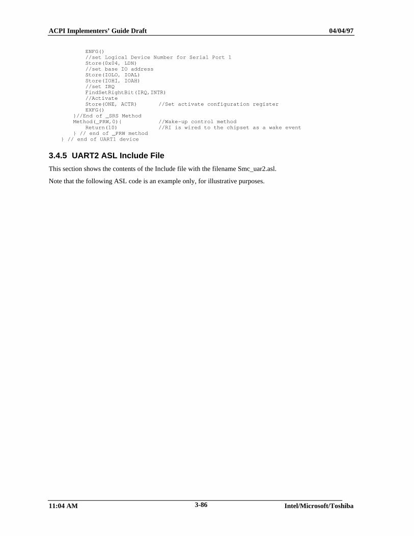
ACPI Implementers’ Guide Draft 04/04/97
11:04 AM Intel/Microsoft/Toshiba3-86
ENFG()//set Logical Device Number for Serial Port 1Store(0x04, LDN)//set base IO addressStore(IOLO, IOAL)Store(IOHI, IOAH)//set IRQFindSetRightBit(IRQ,INTR)//ActivateStore(ONE, ACTR) //Set activate configuration registerEXFG()
}//End of _SRS MethodMethod(_PRW,0){ //Wake-up control method
Return(10) //RI is wired to the chipset as a wake event} // end of _PRW method
} // end of UART1 device
3.4.5 UART2 ASL Include File
This section shows the contents of the Include file with the filename Smc_uar2.asl.
Note that the following ASL code is an example only, for illustrative purposes.
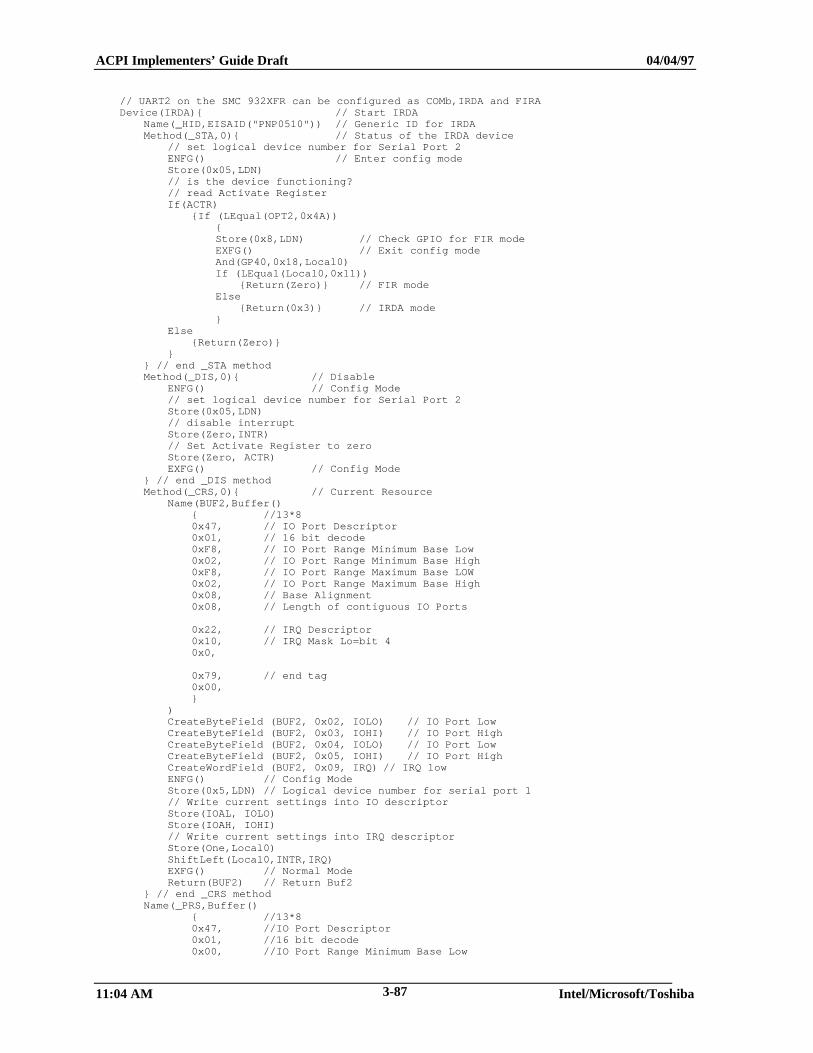
ACPI Implementers’ Guide Draft 04/04/97
11:04 AM Intel/Microsoft/Toshiba3-87
// UART2 on the SMC 932XFR can be configured as COMb,IRDA and FIRADevice(IRDA){ // Start IRDA
Name(_HID,EISAID("PNP0510")) // Generic ID for IRDAMethod(_STA,0){ // Status of the IRDA device
// set logical device number for Serial Port 2ENFG() // Enter config modeStore(0x05,LDN)// is the device functioning?// read Activate RegisterIf(ACTR)
{If (LEqual(OPT2,0x4A)){Store(0x8,LDN) // Check GPIO for FIR modeEXFG() // Exit config modeAnd(GP40,0x18,Local0)If (LEqual(Local0,0x11))
{Return(Zero)} // FIR modeElse
{Return(0x3)} // IRDA mode}
Else{Return(Zero)}
}} // end _STA methodMethod(_DIS,0){ // Disable
ENFG() // Config Mode// set logical device number for Serial Port 2Store(0x05,LDN)// disable interruptStore(Zero,INTR)// Set Activate Register to zeroStore(Zero, ACTR)EXFG() // Config Mode
} // end _DIS methodMethod(_CRS,0){ // Current Resource
Name(BUF2,Buffer(){ //13*80x47, // IO Port Descriptor0x01, // 16 bit decode0xF8, // IO Port Range Minimum Base Low0x02, // IO Port Range Minimum Base High0xF8, // IO Port Range Maximum Base LOW0x02, // IO Port Range Maximum Base High0x08, // Base Alignment0x08, // Length of contiguous IO Ports
0x22, // IRQ Descriptor0x10, // IRQ Mask Lo=bit 40x0,
0x79, // end tag0x00,}
)CreateByteField (BUF2, 0x02, IOLO) // IO Port LowCreateByteField (BUF2, 0x03, IOHI) // IO Port HighCreateByteField (BUF2, 0x04, IOLO) // IO Port LowCreateByteField (BUF2, 0x05, IOHI) // IO Port HighCreateWordField (BUF2, 0x09, IRQ) // IRQ lowENFG() // Config ModeStore(0x5,LDN) // Logical device number for serial port 1// Write current settings into IO descriptorStore(IOAL, IOLO)Store(IOAH, IOHI)// Write current settings into IRQ descriptorStore(One,Local0)ShiftLeft(Local0,INTR,IRQ)EXFG() // Normal ModeReturn(BUF2) // Return Buf2
} // end _CRS methodName(_PRS,Buffer()
{ //13*80x47, //IO Port Descriptor0x01, //16 bit decode0x00, //IO Port Range Minimum Base Low
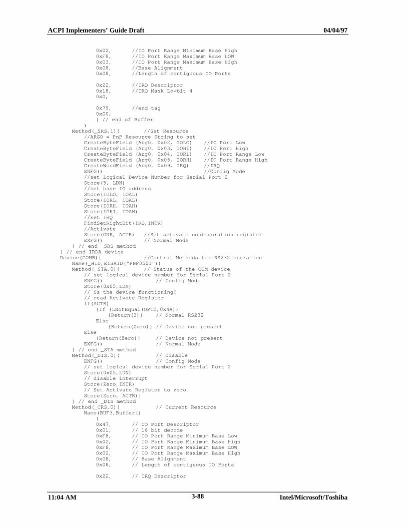
ACPI Implementers’ Guide Draft 04/04/97
11:04 AM Intel/Microsoft/Toshiba3-88
0x02, //IO Port Range Minimum Base High0xF8, //IO Port Range Maximum Base LOW0x03, //IO Port Range Maximum Base High0x08, //Base Alignment0x08, //Length of contiguous IO Ports
0x22, //IRQ Descriptor0x18, //IRQ Mask Lo=bit 40x0,
0x79, //end tag0x00,} // end of Buffer
)Method(_SRS,1){ //Set Resource
//ARG0 = PnP Resource String to setCreateByteField (Arg0, 0x02, IOLO) //IO Port LowCreateByteField (Arg0, 0x03, IOHI) //IO Port HighCreateByteField (Arg0, 0x04, IORL) //IO Port Range LowCreateByteField (Arg0, 0x05, IORH) //IO Port Range HighCreateWordField (Arg0, 0x09, IRQ) //IRQENFG() //Config Mode//set Logical Device Number for Serial Port 2Store(5, LDN)//set base IO addressStore(IOLO, IOAL)Store(IORL, IOAL)Store(IORH, IOAH)Store(IOHI, IOAH)//set IRQFindSetRightBit(IRQ,INTR)//ActivateStore(ONE, ACTR) //Set activate configuration registerEXFG() // Normal Mode
} // end _SRS method} // end IRDA deviceDevice(COMB){ //Control Methods for RS232 operation
Name(_HID,EISAID("PNP0501"))Method(_STA,0){ // Status of the COM device
// set logical device number for Serial Port 2ENFG() // Config ModeStore(0x05,LDN)// is the device functioning?// read Activate RegisterIf(ACTR)
{If (LNotEqual(OPT2,0x4A)){Return(3)} // Normal RS232
Else{Return(Zero)} // Device not present
Else{Return(Zero)} // Device not present
EXFG() // Normal Mode} // end _STA methodMethod(_DIS,0){ // Disable
ENFG() // Config Mode// set logical device number for Serial Port 2Store(0x05,LDN)// disable interruptStore(Zero,INTR)// Set Activate Register to zeroStore(Zero, ACTR)}
} // end _DIS methodMethod(_CRS,0){ // Current Resource
Name(BUF3,Buffer(){0x47, // IO Port Descriptor0x01, // 16 bit decode0xF8, // IO Port Range Minimum Base Low0x02, // IO Port Range Minimum Base High0xF8, // IO Port Range Maximum Base LOW0x02, // IO Port Range Maximum Base High0x08, // Base Alignment0x08, // Length of contiguous IO Ports
0x22, // IRQ Descriptor
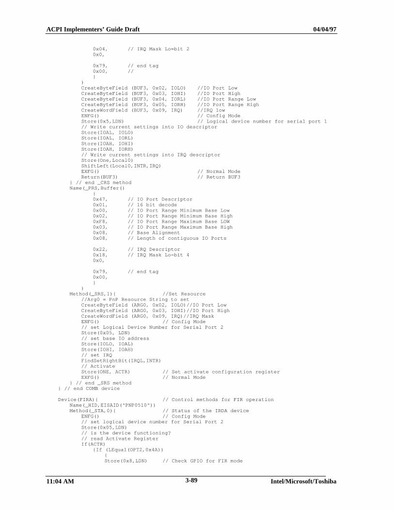
ACPI Implementers’ Guide Draft 04/04/97
11:04 AM Intel/Microsoft/Toshiba3-89
0x04, // IRQ Mask Lo=bit 20x0,
0x79, // end tag0x00, //}
)CreateByteField (BUF3, 0x02, IOLO) //IO Port LowCreateByteField (BUF3, 0x03, IOHI) //IO Port HighCreateByteField (BUF3, 0x04, IORL) //IO Port Range LowCreateByteField (BUF3, 0x05, IORH) //IO Port Range HighCreateWordField (BUF3, 0x09, IRQ) //IRQ lowENFG() // Config ModeStore(0x5,LDN) // Logical device number for serial port 1// Write current settings into IO descriptorStore(IOAL, IOLO)Store(IOAL, IORL)Store(IOAH, IOHI)Store(IOAH, IORH)// Write current settings into IRQ descriptorStore(One,Local0)ShiftLeft(Local0,INTR,IRQ)EXFG() // Normal ModeReturn(BUF3) // Return BUF3
} // end _CRS methodName(_PRS,Buffer()
{0x47, // IO Port Descriptor0x01, // 16 bit decode0x00, // IO Port Range Minimum Base Low0x02, // IO Port Range Minimum Base High0xF8, // IO Port Range Maximum Base LOW0x03, // IO Port Range Maximum Base High0x08, // Base Alignment0x08, // Length of contiguous IO Ports
0x22, // IRQ Descriptor0x18, // IRQ Mask Lo=bit 40x0,
0x79, // end tag0x00,}
)Method(_SRS,1){ //Set Resource
//Arg0 = PnP Resource String to setCreateByteField (ARG0, 0x02, IOLO)//IO Port LowCreateByteField (ARG0, 0x03, IOHI)//IO Port HighCreateWordField (ARG0, 0x09, IRQ)//IRQ MaskENFG() // Config Mode// set Logical Device Number for Serial Port 2Store(0x05, LDN)// set base IO addressStore(IOLO, IOAL)Store(IOHI, IOAH)// set IRQFindSetRightBit(IRQL,INTR)// ActivateStore(ONE, ACTR) // Set activate configuration registerEXFG() // Normal Mode
} // end _SRS method} // end COMB device
Device(FIRA){ // Control methods for FIR operationName(_HID,EISAID("PNP0510"))Method(_STA,0){ // Status of the IRDA device
ENFG() // Config Mode// set logical device number for Serial Port 2Store(0x05,LDN)// is the device functioning?// read Activate RegisterIf(ACTR)
{If (LEqual(OPT2,0x4A)){Store(0x8,LDN) // Check GPIO for FIR mode
ACPI Implementers’ Guide Draft 04/04/97
11:04 AM Intel/Microsoft/Toshiba3-90
And(GP40,0x18,Local0)If (LEqual(Local0,0x11))
{Return(0x3)} // FIR modeElse
{Return(Zero)} // not FIR mode}
}Else
{Return(Zero)}} // end _STA methodMethod(_DIS,0){ //Disable
//set logical device number for Serial Port 2ENFG() // Config ModeStore(0x05,LDN)//Disable DMAStore(Zero,DMCH)//disable interruptStore(Zero,INTR)//Set Activate Register to zeroStore(Zero, ACTR)EXFG() // Normal Mode
} // end _DIS methodMethod(_CRS,0){ //Current Resource
Name(BUF4,Buffer(){ //16*80x47, //IO Port Descriptor0x01, //16 bit decode0xF8, //IO Port Range Minimum Base Low0x02, //IO Port Range Minimum Base High0xF8, //IO Port Range Maximum Base LOW0x02, //IO Port Range Maximum Base High0x08, //Base Alignment0x08, //Length of contiguous IO Ports
0x22, //IRQ Descriptor0x10, //IRQ Mask Lo=bit 40x0,
0x2A, //DMA Descriptor0x0, //DMA Mask0x0, //DMA mode
0x79, //end tag0x00,}
)CreateByteField (BUF4, 0x02, IOLO)//IO Port LowCreateByteField (BUF4, 0x03, IOHI)//IO Port HighCreateByteField (BUF4, 0x04, IOLO)//IO Port LowCreateByteField (BUF4, 0x05, IOHI)//IO Port HighCreateWordField (BUF4, 0x09, IRQ)//IRQ lowCreateByteField (BUF4, 0x0C, DMCH)//DMA MaskENFG() // Config ModeStore(0x5, LDN) //Logical device number for serial port 1//Write current settings into IO descriptorStore(IOAL, IOLO)Store(IOAH, IOHI)//Write current settings into IRQ descriptorStore(One,Local0)ShiftLeft(Local0,INTR,IRQ)EXFG() // Normal ModeReturn(BUF4) // Return BUF4
} // end _CRS methodName(_PRS,Buffer(){ // 16*8
0x47, //IO Port Descriptor0x01, //16 bit decode0xF8, //IO Port Range Minimum Base Low0x02, //IO Port Range Minimum Base High0xF8, //IO Port Range Maximum Base LOW0x02, //IO Port Range Maximum Base High0x08, //Base Alignment0x08, //Length of contiguous IO Ports
0x22, //IRQ Descriptor0x18, //IRQ Mask Lo=bits 3 and 4
ACPI Implementers’ Guide Draft 04/04/97
11:04 AM Intel/Microsoft/Toshiba3-91
0x0,
0x2A, //DMA Descriptor0x0, //DMA Mask0x0, //DMA mode
0x79, //end tag0x00,}
) // end _PRSMethod(_SRS,1){ //Set Resource
//ARG0 = PnP Resource String to setCreateByteField (ARG0, 0x02, IOLO)//IO Port LowCreateByteField (ARG0, 0x03, IOHI)//IO Port HighCreateByteField (ARG0, 0x04, IORL)//IO Port Range LowCreateByteField (ARG0, 0x05, IORH)//IO Port Range HighCreateWordField (ARG0, 0x09, IRQ)//IRQ lowCreateByteField (ARG0, 0x0C, DMAV)//DMAENFG() // Config Mode// set Logical Device Number for Serial Port 2Store(0x05, LDN)// set base IO addressStore(IOLO, IOAL)Store(IORL, IOAL)Store(IORH, IOAH)Store(IOHI, IOAH)// set IRQFindSetRightBit(IRQ,INTR)// Set DMAFindSetRightBit(DMAV,DMCH)// ActivateStore(ONE, ACTR) // Set activate configuration registerEXFG()
} // end _SRS Method} // end FIR device
3.4.6 Printer ASL Include File
This section shows the contents of the Include file with the filename Smc_prt.asl.
Note that the following ASL code is an example only, for illustrative purposes.
ACPI Implementers’ Guide Draft 04/04/97
11:04 AM Intel/Microsoft/Toshiba3-92
// LPT DEVICEDevice(LPT) {
Name (_HID, EISAID("PNP0400")) // PnP ID for SMC LPT PortMethod (_STA, 0) { // LPT Device Status
ENFG() // Config ModeAnd(OPT1,0x7,Local0) // Extract mode bitsIf (LEqual(Local0, 0x4)){
If (ACTR){Return(3)} // Device present and active
Else{Return(One)} // Not present
}//Present not activeElse
{Return(0) //Not present}EXFG()
} // end of _STA methodMethod (_DIS) { // LPT Device Disable
ENFG()Store (0x03,LDN) // Select PRN Device (LDN = 03)Store (Zero, INTR) // disable INTRStore (Zero, ACTR) // Set Activate Reg = 0EXFG()
} // End of _DIS Method// LPT _CRS METHODMethod (_CRS) { // LPT Current ResourcesName(BUF5, Buffer ()
{ //13*8 Length of Buffer0x47, // IO port descriptor0x01, // 16 bit decode0x78, // LPT1 @ 0x278h0x02,0x78,0x02,0x08, //alignment0x08, //number of ports
0x22, // IRQ Descriptor0x80, // IRQ7 (Bit15=IRQ15....Bit0=IRQ0)0x00,
// No DMA
0x79, //end tag0x00,} // end of Buffer
) // end _CRS method//--------- Name the fields within the bufferCreateByteField (BUF5, 0x02, IOLO)CreateByteField (BUF5, 0x03, IOHI)CreateByteField (BUF5, 0x04, IORL) // IO Port LowCreateByteField (BUF5, 0x05, IORH) // IO Port HICreateWordField (BUF5, 0x09, IRQW)//--------- Read Devices PnP Config Regs into BufferENFG()Store (0x03, LDN) //Select Logical Device 3 (LPT)STORE(IOAL, IOLO) // Write IO Port LOW to dev cfg bufferSTORE(IOAL, IORL)STORE(IOAH, IOHI) //Write IO Port High to dev cfg bufferSTORE(IOAH, IOAH)//---convert INTR(3:0) to single bit represetation of IRQStore(One,Local0)ShiftLeft(Local0,INTR,IRQW) // (src, shiftcount, result)EXFG()Return(BUF5) // return BUF3 filled with Current Resources
} // end _CRS method// LPT _PRS METHOD ---------------------------------------// Create buffer with possible resources (pnp descriptor)// Assume _PRS defines Resource Ordering [{IO,IRQ} vs {IRQ,IO}] in _CRS & _SRS methodsName(_PRS, Buffer()
{ //13*80x30, // Start Dependent Function
0x47, // IO port descriptor0x01, // 16 bit decode0x78, // LPT1 @ 0x278h
ACPI Implementers’ Guide Draft 04/04/97
11:04 AM Intel/Microsoft/Toshiba3-93
0x03,0x78,0x03,0x08, // alignment0x04, // number of ports
0x22, // IRQ Descriptor0x80, // IRQ7 (Bit15=IRQ15....Bit0=IRQ0)0x00,
// No DMA0x38, // End Dependent Function
0x30, // Start Dependent Function
0x47, // IO port descriptor0x01, // 16 bit decode0x78, // LPT1 @ 0x278h0x02,0x78,0x02,
0x08, // alignment0x04, // number of ports
0x22, // IRQ Descriptor0xA0, // IRQ5 (Bit15=IRQ15....Bit0=IRQ0)0x00,
// No DMA0x38, // End Dependent Function
0x30, // Start Dependent Function
0x47, // IO port descriptor0x01, // 16 bit decode0xBC, // LPT1 @ 0x278h0x03,0xBC,0x03,
0x08, // alignment0x04, // number of ports
0x22, // IRQ Descriptor0xA0, // IRQ5 (Bit15=IRQ15....Bit0=IRQ0)0x00,
// No DMA0x38, // End Dependent Function
0x79, //end tag0x00,} // end of Buffer
) // end _PRS method
// LPT _SRS METHOD -----------------------------------------------------Method ( _SRS,1 ) { // LPT Set Resources & Enables the Device
// Arg0 = PnP Resource String to Set// (IO,IRQ ordering assumed to be same as _PRS/_CRS)// name the fields within the Arg0 String ---------------------CreateByteField (Arg0, 0x02, IOLO) // IO Port LowCreateByteField (Arg0, 0x03, IOHI) // IO Port HICreateByteField (Arg0, 0x04, IORL) // IO Port LowCreateByteField (Arg0, 0x05, IORH) // IO Port HICreateWordField (Arg0, 0x06, IRQW) // IRQ MASKENFG()// Set the requested resources on the deviceStore(0x03, LDN) // Select LDN #3 (LPT)Store(IOLO, IOAL) // Write IO Port LOW to dev cfg regStore(IOHI, IOAH)// Convert setbit position in IRQL:IRQH into 4bit field and write to PnP INTR regFindSetLeftBit(IRQW, INTR) // Wr requested IRQStore(One, ACTR) // Active (ie Enable) the DeviceEXFG()
} // end of _SRS Method} // end LPT device
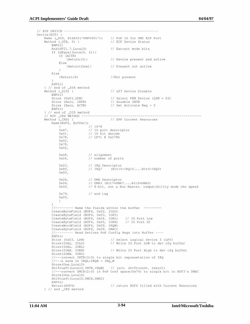
ACPI Implementers’ Guide Draft 04/04/97
11:04 AM Intel/Microsoft/Toshiba3-94
// ECP DEVICE ------------------------------------------------Device(ECP) {
Name (_HID, EISAID("PNP0401")) // PnP ID for SMC ECP PortMethod (_STA, 0) { // ECP Device Status
ENFG()And(OPT1,7,Local0) // Extract mode bitsIf (LEqual(Local0, 2)){
If (ACTR){Return(3)} // Device present and active
Else{Return(One)} // Present not active
}Else
{Return(0) //Not present}EXFG()
} // end of _STA methodMethod (_DIS) { // LPT Device Disable
ENFG()Store (0x03,LDN) // Select PRN Device (LDN = 03)Store (Zero, INTR) // disable INTRStore (Zero, ACTR) // Set Activate Reg = 0EXFG()
} // end of _DIS method// ECP _CRS METHOD -------------------------------------------------------------
Method (_CRS) { // EPP Current ResourcesName(BUF6, Buffer()
{ // 16*80x47, // IO port descriptor0x01, // 16 bit decode0x78, // LPT1 @ 0x278h0x02,0x78,0x02,
0x08, // alignment0x04, // number of ports
0x22, // IRQ Descriptor0x80, // IRQ7 (Bit15=IRQ15....Bit0=IRQ0)0x00,
0x2A, // DMA Descriptor0x04, // DMA3 (Bit7=DMA7....Bit0=DMA0)0x00, // 8-bit, not a Bus Master, compatibility mode chn speed
0x79, // end tag0x00,}
)//--------- Name the fields within the buffer ---------CreateByteField (BUF6, 0x02, IOLO)CreateByteField (BUF6, 0x03, IOHI)CreateByteField (BUF6, 0x04, IORL) // IO Port LowCreateByteField (BUF6, 0x05, IORH) // IO Port HICreateWordField (BUF6, 0x09, IRQW)CreateByteField (BUF6, 0x09, DMAC)//--------- Read Devices PnP Config Regs into Buffer ----ENFG()Store (0x03, LDN) // Select Logical Device 3 (LPT)Store(IOAL, IOLO) // Write IO Port LOW to dev cfg bufferStore(IOAL, IORL)Store(IOAH, IORH) // Write IO Port High to dev cfg bufferStore(IOAH, IOHI)//---convert INTR(3:0) to single bit represetation of IRQ//---& save in IRQL:IRQH = IRQ_WStore(One,Local0)ShiftLeft(Local0,INTR,IRQW) // (src, shiftcount, result)//---convert DMCH(2:0) in PnP Conf space(0x74) to single bit in BUF3's DMACStore(One,Local0)ShiftLeft(Local0,DMCH,DMAC)EXFG()Return(BUF6) // return BUF6 filled with Current Resources
} // end _CRS method
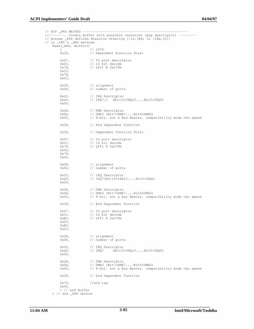
ACPI Implementers’ Guide Draft 04/04/97
11:04 AM Intel/Microsoft/Toshiba3-95
// ECP _PRS METHOD -----------------------------------------------------//--------- Create buffer with possible resources (pnp descriptor) ---------// Assume _PRS defines Resource Ordering [{IO,IRQ} vs {IRQ,IO}]// in _CRS & _SRS methods
Name(_PRS, Buffer(){ // 16*80x30, // Dependent Function Start
0x47, // IO port descriptor0x01, // 16 bit decode0x78, // LPT1 @ 0x278h0x03,0x78,0x03,
0x08, // alignment0x04, // number of ports
0x22, // IRQ Descriptor0xa0, // IRQ7,5 (Bit15=IRQ15....Bit0=IRQ0)0x00,
0x2A, // DMA Descriptor0x0b, // DMA3 (Bit7=DMA7....Bit0=DMA0)0x00, // 8-bit, not a Bus Master, compatibility mode chn speed
0x38, // End Dependent Function
0x30, // Dependent Function Start
0x47, // IO port descriptor0x01, // 16 bit decode0x78, // LPT1 @ 0x278h0x02,0x78,0x02,
0x08, // alignment0x04, // number of ports
0x22, // IRQ Descriptor0xa0, // IRQ7(Bit15=IRQ15....Bit0=IRQ0)0x00,
0x2A, // DMA Descriptor0x0b, // DMA3 (Bit7=DMA7....Bit0=DMA0)0x00, // 8-bit, not a Bus Master, compatibility mode chn speed
0x38, // End Dependent Function
0x47, // IO port descriptor0x01, // 16 bit decode0xBC, // LPT1 @ 0x278h0x03,0xBC,0x03,
0x08, // alignment0x04, // number of ports
0x22, // IRQ Descriptor0xa0, // IRQ7 (Bit15=IRQ15....Bit0=IRQ0)0x00,
0x2A, // DMA Descriptor0x0b, // DMA3 (Bit7=DMA7....Bit0=DMA0)0x00, // 8-bit, not a Bus Master, compatibility mode chn speed
0x38, // End Dependent Function
0x79, //end tag0x00,} // end Buffer
) // end _PRS method
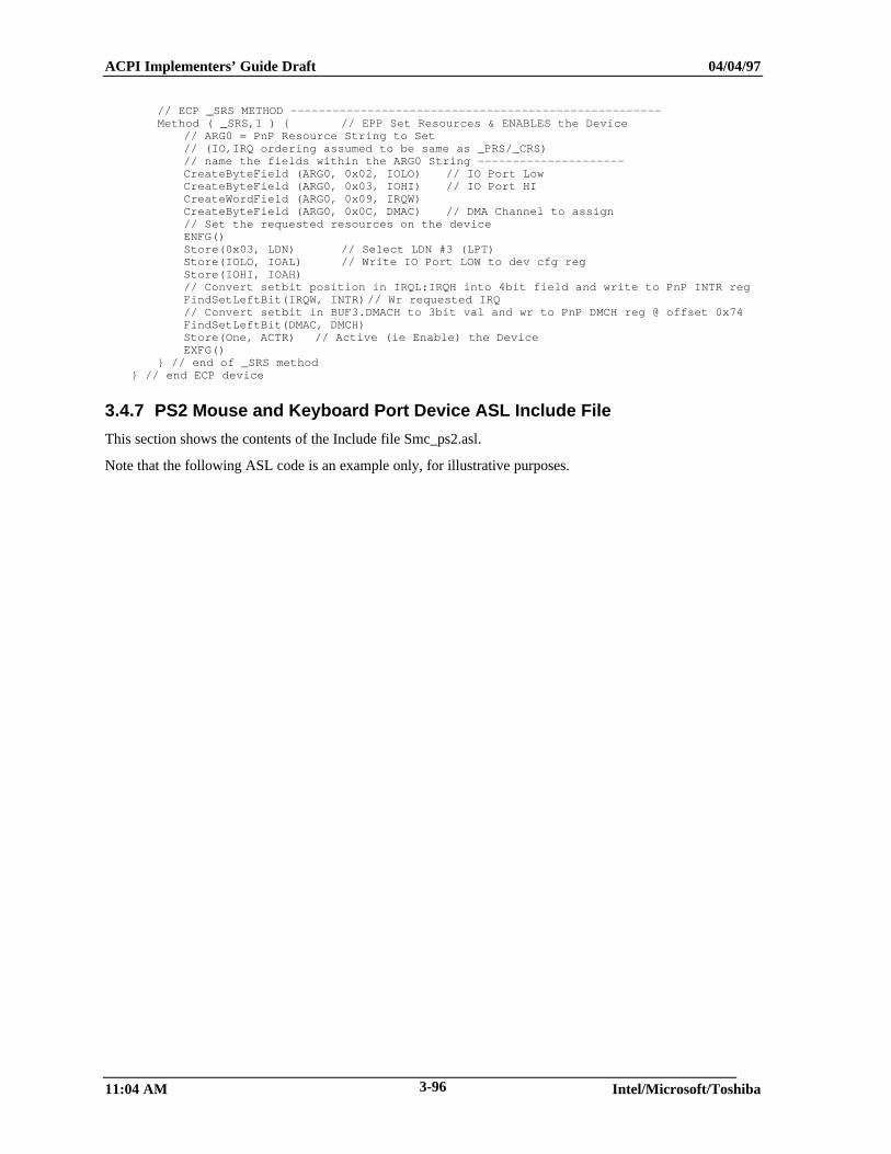
ACPI Implementers’ Guide Draft 04/04/97
11:04 AM Intel/Microsoft/Toshiba3-96
// ECP _SRS METHOD -----------------------------------------------------Method ( _SRS,1 ) { // EPP Set Resources & ENABLES the Device
// ARG0 = PnP Resource String to Set// (IO,IRQ ordering assumed to be same as _PRS/_CRS)// name the fields within the ARG0 String ---------------------CreateByteField (ARG0, 0x02, IOLO) // IO Port LowCreateByteField (ARG0, 0x03, IOHI) // IO Port HICreateWordField (ARG0, 0x09, IRQW)CreateByteField (ARG0, 0x0C, DMAC) // DMA Channel to assign// Set the requested resources on the deviceENFG()Store(0x03, LDN) // Select LDN #3 (LPT)Store(IOLO, IOAL) // Write IO Port LOW to dev cfg regStore(IOHI, IOAH)// Convert setbit position in IRQL:IRQH into 4bit field and write to PnP INTR regFindSetLeftBit(IRQW, INTR)// Wr requested IRQ// Convert setbit in BUF3.DMACH to 3bit val and wr to PnP DMCH reg @ offset 0x74FindSetLeftBit(DMAC, DMCH)Store(One, ACTR) // Active (ie Enable) the DeviceEXFG()
} // end of _SRS method} // end ECP device
3.4.7 PS2 Mouse and Keyboard Port Device ASL Include File
This section shows the contents of the Include file Smc_ps2.asl.
Note that the following ASL code is an example only, for illustrative purposes.
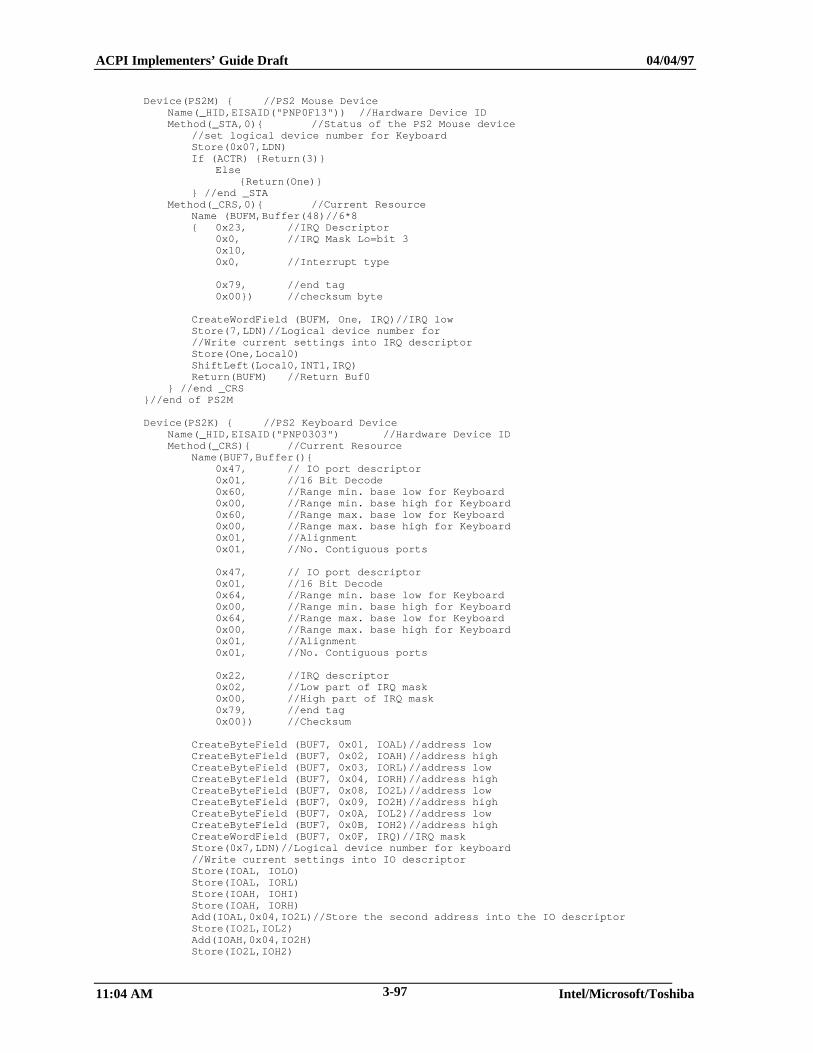
ACPI Implementers’ Guide Draft 04/04/97
11:04 AM Intel/Microsoft/Toshiba3-97
Device(PS2M) { //PS2 Mouse DeviceName(_HID,EISAID("PNP0F13")) //Hardware Device IDMethod(_STA,0){ //Status of the PS2 Mouse device
//set logical device number for KeyboardStore(0x07,LDN)If (ACTR) {Return(3)}
Else{Return(One)}
} //end _STAMethod(_CRS,0){ //Current Resource
Name (BUFM,Buffer(48)//6*8{ 0x23, //IRQ Descriptor
0x0, //IRQ Mask Lo=bit 30x10,0x0, //Interrupt type
0x79, //end tag0x00}) //checksum byte
CreateWordField (BUFM, One, IRQ)//IRQ lowStore(7,LDN)//Logical device number for//Write current settings into IRQ descriptorStore(One,Local0)ShiftLeft(Local0,INT1,IRQ)Return(BUFM) //Return Buf0
} //end _CRS}//end of PS2M
Device(PS2K) { //PS2 Keyboard DeviceName(_HID,EISAID("PNP0303") //Hardware Device IDMethod(_CRS){ //Current Resource
Name(BUF7,Buffer(){0x47, // IO port descriptor0x01, //16 Bit Decode0x60, //Range min. base low for Keyboard0x00, //Range min. base high for Keyboard0x60, //Range max. base low for Keyboard0x00, //Range max. base high for Keyboard0x01, //Alignment0x01, //No. Contiguous ports
0x47, // IO port descriptor0x01, //16 Bit Decode0x64, //Range min. base low for Keyboard0x00, //Range min. base high for Keyboard0x64, //Range max. base low for Keyboard0x00, //Range max. base high for Keyboard0x01, //Alignment0x01, //No. Contiguous ports
0x22, //IRQ descriptor0x02, //Low part of IRQ mask0x00, //High part of IRQ mask0x79, //end tag0x00}) //Checksum
CreateByteField (BUF7, 0x01, IOAL)//address lowCreateByteField (BUF7, 0x02, IOAH)//address highCreateByteField (BUF7, 0x03, IORL)//address lowCreateByteField (BUF7, 0x04, IORH)//address highCreateByteField (BUF7, 0x08, IO2L)//address lowCreateByteField (BUF7, 0x09, IO2H)//address highCreateByteField (BUF7, 0x0A, IOL2)//address lowCreateByteField (BUF7, 0x0B, IOH2)//address highCreateWordField (BUF7, 0x0F, IRQ)//IRQ maskStore(0x7,LDN)//Logical device number for keyboard//Write current settings into IO descriptorStore(IOAL, IOLO)Store(IOAL, IORL)Store(IOAH, IOHI)Store(IOAH, IORH)Add(IOAL,0x04,IO2L)//Store the second address into the IO descriptorStore(IO2L,IOL2)Add(IOAH,0x04,IO2H)Store(IO2L,IOH2)
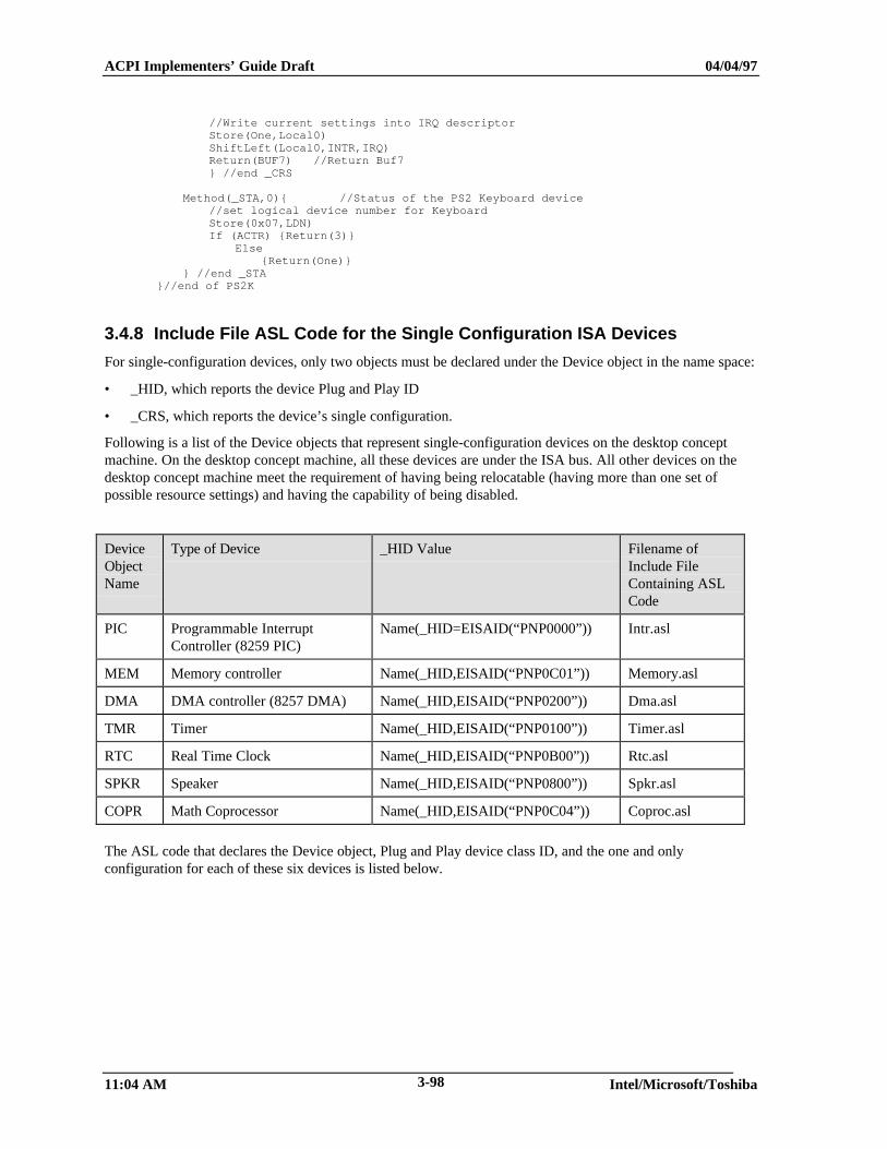
ACPI Implementers’ Guide Draft 04/04/97
11:04 AM Intel/Microsoft/Toshiba3-98
//Write current settings into IRQ descriptorStore(One,Local0)ShiftLeft(Local0,INTR,IRQ)Return(BUF7) //Return Buf7} //end _CRS
Method(_STA,0){ //Status of the PS2 Keyboard device//set logical device number for KeyboardStore(0x07,LDN)If (ACTR) {Return(3)}
Else{Return(One)}
} //end _STA}//end of PS2K
3.4.8 Include File ASL Code for the Single Configuration ISA Devices
For single-configuration devices, only two objects must be declared under the Device object in the name space:
• _HID, which reports the device Plug and Play ID
• _CRS, which reports the device’s single configuration.
Following is a list of the Device objects that represent single-configuration devices on the desktop conceptmachine. On the desktop concept machine, all these devices are under the ISA bus. All other devices on thedesktop concept machine meet the requirement of having being relocatable (having more than one set ofpossible resource settings) and having the capability of being disabled.
DeviceObjectName
Type of Device _HID Value Filename ofInclude FileContaining ASLCode
PIC Programmable InterruptController (8259 PIC)
Name(_HID=EISAID(“PNP0000”)) Intr.asl
MEM Memory controller Name(_HID,EISAID(“PNP0C01”)) Memory.asl
DMA DMA controller (8257 DMA) Name(_HID,EISAID(“PNP0200”)) Dma.asl
TMR Timer Name(_HID,EISAID(“PNP0100”)) Timer.asl
RTC Real Time Clock Name(_HID,EISAID(“PNP0B00”)) Rtc.asl
SPKR Speaker Name(_HID,EISAID(“PNP0800”)) Spkr.asl
COPR Math Coprocessor Name(_HID,EISAID(“PNP0C04”)) Coproc.asl
The ASL code that declares the Device object, Plug and Play device class ID, and the one and onlyconfiguration for each of these six devices is listed below.
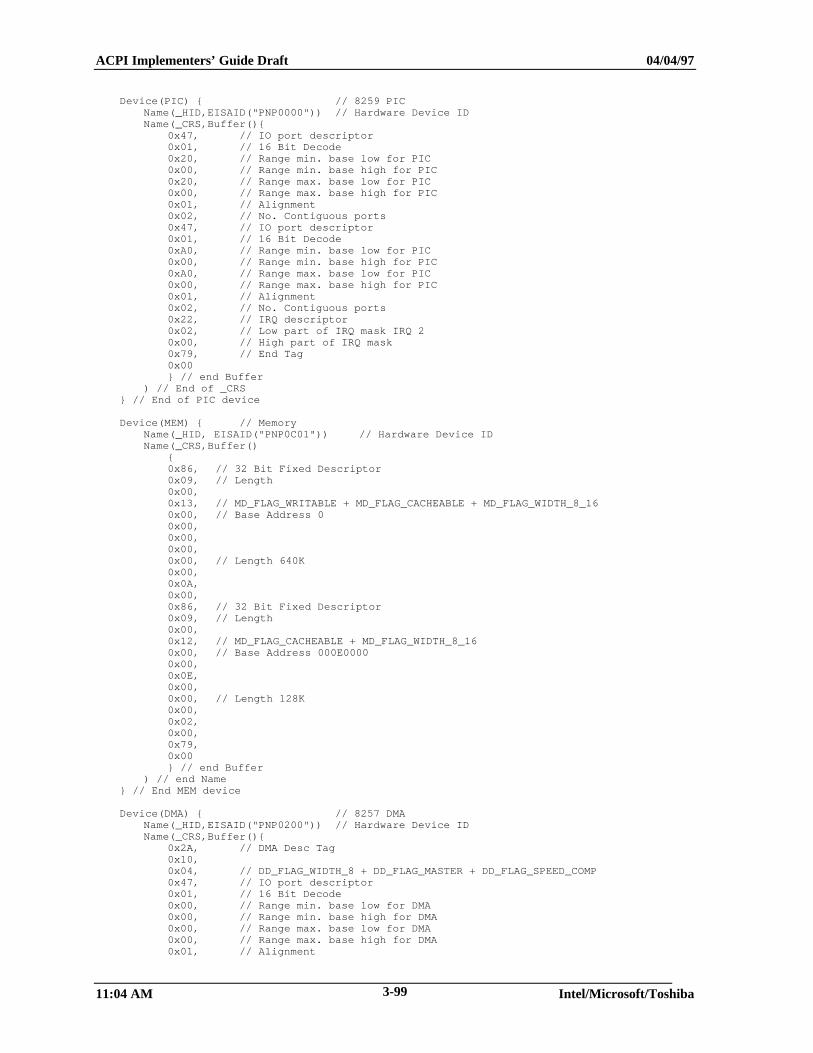
ACPI Implementers’ Guide Draft 04/04/97
11:04 AM Intel/Microsoft/Toshiba3-99
Device(PIC) { // 8259 PICName(_HID,EISAID("PNP0000")) // Hardware Device IDName(_CRS,Buffer(){
0x47, // IO port descriptor0x01, // 16 Bit Decode0x20, // Range min. base low for PIC0x00, // Range min. base high for PIC0x20, // Range max. base low for PIC0x00, // Range max. base high for PIC0x01, // Alignment0x02, // No. Contiguous ports0x47, // IO port descriptor0x01, // 16 Bit Decode0xA0, // Range min. base low for PIC0x00, // Range min. base high for PIC0xA0, // Range max. base low for PIC0x00, // Range max. base high for PIC0x01, // Alignment0x02, // No. Contiguous ports0x22, // IRQ descriptor0x02, // Low part of IRQ mask IRQ 20x00, // High part of IRQ mask0x79, // End Tag0x00} // end Buffer
) // End of _CRS} // End of PIC device
Device(MEM) { // MemoryName(_HID, EISAID("PNP0C01")) // Hardware Device IDName(_CRS,Buffer()
{0x86, // 32 Bit Fixed Descriptor0x09, // Length0x00,0x13, // MD_FLAG_WRITABLE + MD_FLAG_CACHEABLE + MD_FLAG_WIDTH_8_160x00, // Base Address 00x00,0x00,0x00,0x00, // Length 640K0x00,0x0A,0x00,0x86, // 32 Bit Fixed Descriptor0x09, // Length0x00,0x12, // MD_FLAG_CACHEABLE + MD_FLAG_WIDTH_8_160x00, // Base Address 000E00000x00,0x0E,0x00,0x00, // Length 128K0x00,0x02,0x00,0x79,0x00} // end Buffer
) // end Name} // End MEM device
Device(DMA) { // 8257 DMAName(_HID,EISAID("PNP0200")) // Hardware Device IDName(_CRS,Buffer(){
0x2A, // DMA Desc Tag0x10,0x04, // DD_FLAG_WIDTH_8 + DD_FLAG_MASTER + DD_FLAG_SPEED_COMP0x47, // IO port descriptor0x01, // 16 Bit Decode0x00, // Range min. base low for DMA0x00, // Range min. base high for DMA0x00, // Range max. base low for DMA0x00, // Range max. base high for DMA0x01, // Alignment
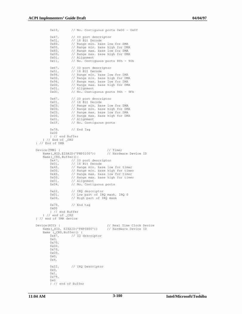
ACPI Implementers’ Guide Draft 04/04/97
11:04 AM Intel/Microsoft/Toshiba3-100
0x10, // No. Contiguous ports 0x00 - 0x0f
0x47, // IO port descriptor0x01, // 16 Bit Decode0x80, // Range min. base low for DMA0x00, // Range min. base high for DMA0x80, // Range max. base low for DMA0x00, // Range max. base high for DMA0x01, // Alignment0x11, // No. Contiguous ports 80h - 90h
0x47, // IO port descriptor0x01, // 16 Bit Decode0x94, // Range min. base low for DMA0x00, // Range min. base high for DMA0x94, // Range max. base low for DMA0x00, // Range max. base high for DMA0x01, // Alignment0x0C, // No. Contiguous ports 94h - 9Fh
0x47, // IO port descriptor0x01, // 16 Bit Decode0xC0, // Range min. base low for DMA0x00, // Range min. base high for DMA0xC0, // Range max. base low for DMA0x00, // Range max. base high for DMA0x01, // Alignment0x1F, // No. Contiguous ports
0x79, // End Tag0x00} // end Buffer
) // End of _CRS} // End of DMA
Device(TMR) { // TimerName(_HID,EISAID("PNP0100")) // Hardware Device IDName(_CRS,Buffer(){
0x47, // IO port descriptor0x01, // 16 Bit Decode0x40, // Range min. base low for timer0x00, // Range min. base high for timer0x40, // Range max. base low for timer0x00, // Range max. base high for timer0x01, // Alignment0x04, // No. Contiguous ports
0x22, // IRQ descriptor0x01, // Low part of IRQ mask, IRQ 00x00, // High part of IRQ mask
0x79, // End tag0x00} // end Buffer
) // end of _CRS} // end of TMR device
Device(RTC) { // Real Time Clock DeviceName(_HID, EISAID("PNP0B00")) // Hardware Device IDName (_CRS,Buffer() {
0x47, // IO descriptor0x0,0x70,0x00,0x70,0x00,0x0,0x4,
0x22, // IRQ Descriptor0x0,0x1,0x79,0x0} // end of Buffer
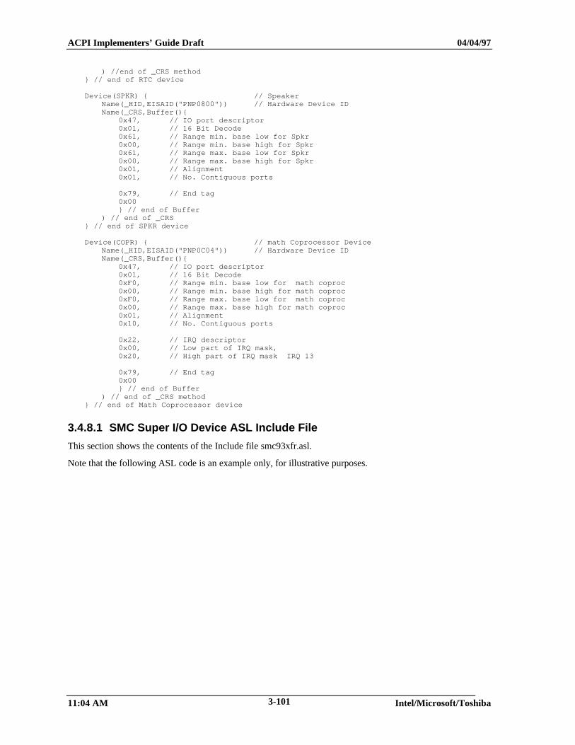
ACPI Implementers’ Guide Draft 04/04/97
11:04 AM Intel/Microsoft/Toshiba3-101
) //end of _CRS method} // end of RTC device
Device(SPKR) { // SpeakerName(_HID,EISAID("PNP0800")) // Hardware Device IDName(_CRS,Buffer(){
0x47, // IO port descriptor0x01, // 16 Bit Decode0x61, // Range min. base low for Spkr0x00, // Range min. base high for Spkr0x61, // Range max. base low for Spkr0x00, // Range max. base high for Spkr0x01, // Alignment0x01, // No. Contiguous ports
0x79, // End tag0x00} // end of Buffer
) // end of _CRS} // end of SPKR device
Device(COPR) { // math Coprocessor DeviceName(_HID,EISAID("PNP0C04")) // Hardware Device IDName(_CRS,Buffer(){
0x47, // IO port descriptor0x01, // 16 Bit Decode0xF0, // Range min. base low for math coproc0x00, // Range min. base high for math coproc0xF0, // Range max. base low for math coproc0x00, // Range max. base high for math coproc0x01, // Alignment0x10, // No. Contiguous ports
0x22, // IRQ descriptor0x00, // Low part of IRQ mask,0x20, // High part of IRQ mask IRQ 13
0x79, // End tag0x00} // end of Buffer
) // end of _CRS method} // end of Math Coprocessor device
3.4.8.1 SMC Super I/O Device ASL Include File
This section shows the contents of the Include file smc93xfr.asl.
Note that the following ASL code is an example only, for illustrative purposes.
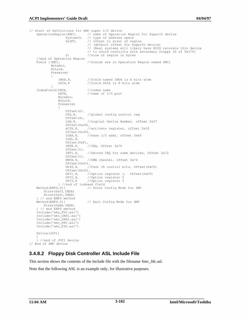
ACPI Implementers’ Guide Draft 04/04/97
11:04 AM Intel/Microsoft/Toshiba3-102
// Start of Definitions for SMC super I/O deviceOperationRegion(SMC1, // name of Operation Region for SuperIO device
SystemIO, // type of address space0x3F0, // offset to start of region
// (default offset for SuperIO device)// (Real systems will likely have BIOS relocate this device// to avoid conflicts with secondary floppy ID of 0x370)
2) //size of region in bytes//end of Operation RegionField ( SMC1, //fields are in Operation Region named SMC1
ByteAcc,NoLock,Preserve){
INDX,8, //field named INDX is b bits wideDATA,8 //field DATA is 8 bits wide
}IndexField(INDX, //index name
DATA, //name of I/O portByteAcc,NoLock,Preserve){
Offset(2),CFG,8, //global config control regOffset(4),LDN,8, //Logical Device Number, offset 0x07Offset(0x28),ACTR,8, //activate register, offset 0x30Offset(0x30),IOAH,8, //base I/O addr, offset 0x60IOAL,8,Offset(0xF),INTR,8, //IRQ, Offset 0x70Offset(1),INT1,8, //Second IRQ for some devices, Offset 0x72Offset(1),DMCH,8, //DMA channel, offset 0x74Offset(0x4C),GP40,8, //Fast IR control bits, Offset(0xC0)Offset(0x30),OPT1,8, //Option register 1, Offset(0xF0)OPT2,8, //Option register 2OPT3,8 //Option register 3
} //end of indexed fieldMethod(ENFG,0){ // Enter Config Mode for SMC
Store(0x55,INDX)Store(0x55,INDX)
} // end ENFG methodMethod(EXFG,0){ // Exit Config Mode for SMC
Store(0xAA,INDX)} // end EXFG methodInclude("smc_FDC.asl")Include("smc_UAR1.asl")Include("smc_UAR2.asl")Include("smc_PRT.asl")Include("smc_PS2.asl")
Device(JOY1){} //end of JOY1 device
// End of SMC device
3.4.8.2 Floppy Disk Controller ASL Include File
This section shows the contents of the Include file with the filename Smc_fdc.asl.
Note that the following ASL is an example only, for illustrative purposes.
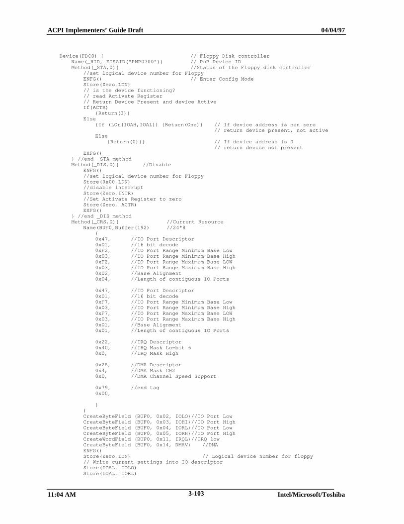
ACPI Implementers’ Guide Draft 04/04/97
11:04 AM Intel/Microsoft/Toshiba3-103
Device(FDC0) { // Floppy Disk controllerName(_HID, EISAID("PNP0700")) // PnP Device IDMethod(_STA,0){ //Status of the Floppy disk controller
//set logical device number for FloppyENFG() // Enter Config ModeStore(Zero,LDN)// is the device functioning?// read Activate Register// Return Device Present and device ActiveIf(ACTR)
{Return(3)}Else
{If (LOr(IOAH,IOAL)) {Return(One)} // If device address is non zero// return device present, not active
Else{Return(0)}} // If device address is 0
// return device not presentEXFG()
} //end _STA methodMethod(_DIS,0){ //Disable
ENFG()//set logical device number for FloppyStore(0x00,LDN)//disable interruptStore(Zero,INTR)//Set Activate Register to zeroStore(Zero, ACTR)EXFG()
} //end _DIS methodMethod(_CRS,0){ //Current Resource
Name(BUF0,Buffer(192) //24*8{0x47, //IO Port Descriptor0x01, //16 bit decode0xF2, //IO Port Range Minimum Base Low0x03, //IO Port Range Minimum Base High0xF2, //IO Port Range Maximum Base LOW0x03, //IO Port Range Maximum Base High0x02, //Base Alignment0x04, //Length of contiguous IO Ports
0x47, //IO Port Descriptor0x01, //16 bit decode0xF7, //IO Port Range Minimum Base Low0x03, //IO Port Range Minimum Base High0xF7, //IO Port Range Maximum Base LOW0x03, //IO Port Range Maximum Base High0x01, //Base Alignment0x01, //Length of contiguous IO Ports
0x22, //IRQ Descriptor0x40, //IRQ Mask Lo=bit 60x0, //IRQ Mask High
0x2A, //DMA Descriptor0x4, //DMA Mask CH20x0, //DMA Channel Speed Support
0x79, //end tag0x00,
})CreateByteField (BUF0, 0x02, IOLO)//IO Port LowCreateByteField (BUF0, 0x03, IOHI)//IO Port HighCreateByteField (BUF0, 0x04, IORL)//IO Port LowCreateByteField (BUF0, 0x05, IORH)//IO Port HighCreateWordField (BUF0, 0x11, IRQL)//IRQ lowCreateByteField (BUF0, 0x14, DMAV) //DMAENFG()Store(Zero,LDN) // Logical device number for floppy// Write current settings into IO descriptorStore(IOAL, IOLO)Store(IOAL, IORL)
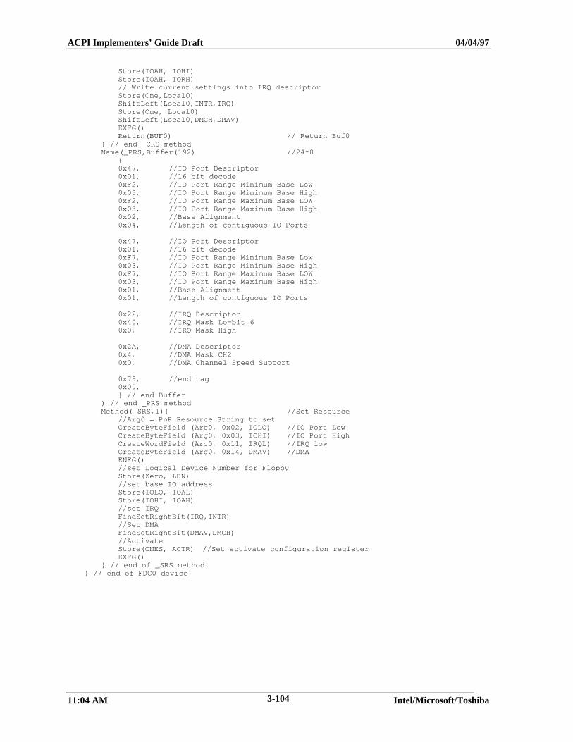
ACPI Implementers’ Guide Draft 04/04/97
11:04 AM Intel/Microsoft/Toshiba3-104
Store(IOAH, IOHI)Store(IOAH, IORH)// Write current settings into IRQ descriptorStore(One,Local0)ShiftLeft(Local0,INTR,IRQ)Store(One, Local0)ShiftLeft(Local0,DMCH,DMAV)EXFG()Return(BUF0) // Return Buf0
} // end _CRS methodName(_PRS,Buffer(192) //24*8
{0x47, //IO Port Descriptor0x01, //16 bit decode0xF2, //IO Port Range Minimum Base Low0x03, //IO Port Range Minimum Base High0xF2, //IO Port Range Maximum Base LOW0x03, //IO Port Range Maximum Base High0x02, //Base Alignment0x04, //Length of contiguous IO Ports
0x47, //IO Port Descriptor0x01, //16 bit decode0xF7, //IO Port Range Minimum Base Low0x03, //IO Port Range Minimum Base High0xF7, //IO Port Range Maximum Base LOW0x03, //IO Port Range Maximum Base High0x01, //Base Alignment0x01, //Length of contiguous IO Ports
0x22, //IRQ Descriptor0x40, //IRQ Mask Lo=bit 60x0, //IRQ Mask High
0x2A, //DMA Descriptor0x4, //DMA Mask CH20x0, //DMA Channel Speed Support
0x79, //end tag0x00,} // end Buffer
) // end _PRS methodMethod(_SRS,1){ //Set Resource
//Arg0 = PnP Resource String to setCreateByteField (Arg0, 0x02, IOLO) //IO Port LowCreateByteField (Arg0, 0x03, IOHI) //IO Port HighCreateWordField (Arg0, 0x11, IRQL) //IRQ lowCreateByteField (Arg0, 0x14, DMAV) //DMAENFG()//set Logical Device Number for FloppyStore(Zero, LDN)//set base IO addressStore(IOLO, IOAL)Store(IOHI, IOAH)//set IRQFindSetRightBit(IRQ,INTR)//Set DMAFindSetRightBit(DMAV,DMCH)//ActivateStore(ONES, ACTR) //Set activate configuration registerEXFG()
} // end of _SRS method} // end of FDC0 device
ACPI Implementers’ Guide Draft 04/04/97
11:04 AM Intel/Microsoft/Toshiba4-105
4. ACPI Server Concept Machine
This section presents the ACPI server concept machine. The hardware components of the server conceptmachine are described by a series of hardware block diagrams. The ACPI name space that models thehardware block diagram is shown, along with sample ASL code that implements the objects in the ACPI namespace.
4.1 Overview of the Server Concept Machine Design
The server concept machine can be characterized as follows:
• Four processors.
• Dual root bridges.
• ACPI hardware support built into the chipset.
• Wake events can come from the LAN controller or the modem.
• Implements the following power saving states:
• System states S1, S4, and S5.
• Processor states C0, C1, and C2.
• Device states D0 and D3. The most prominent device state feature is that SCSI devices are swappablewithout system power down.
The relationships between the server concept machine components are illustrated in the following simplifiedblock diagram:
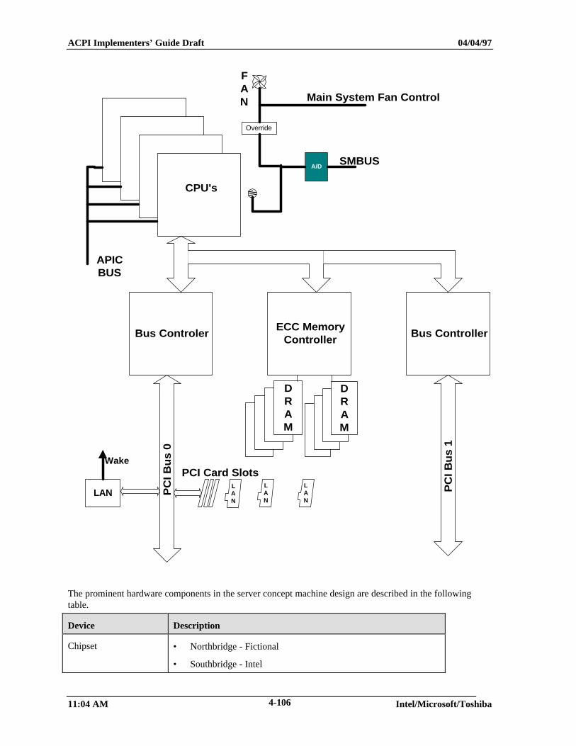
ACPI Implementers’ Guide Draft 04/04/97
11:04 AM Intel/Microsoft/Toshiba4-106
CPU's
Bus ControlerECC Memory
ControllerBus Controller
PC
I Bu
s 0
PC
I Bu
s 1
DRAM
DRAM
PCI Card SlotsLAN
LAN
LAN
A/DSMBUS
FAN
Override
Main System Fan Control
APICBUS
LAN
Wake
The prominent hardware components in the server concept machine design are described in the followingtable.
Device Description
Chipset • Northbridge - Fictional
• Southbridge - Intel
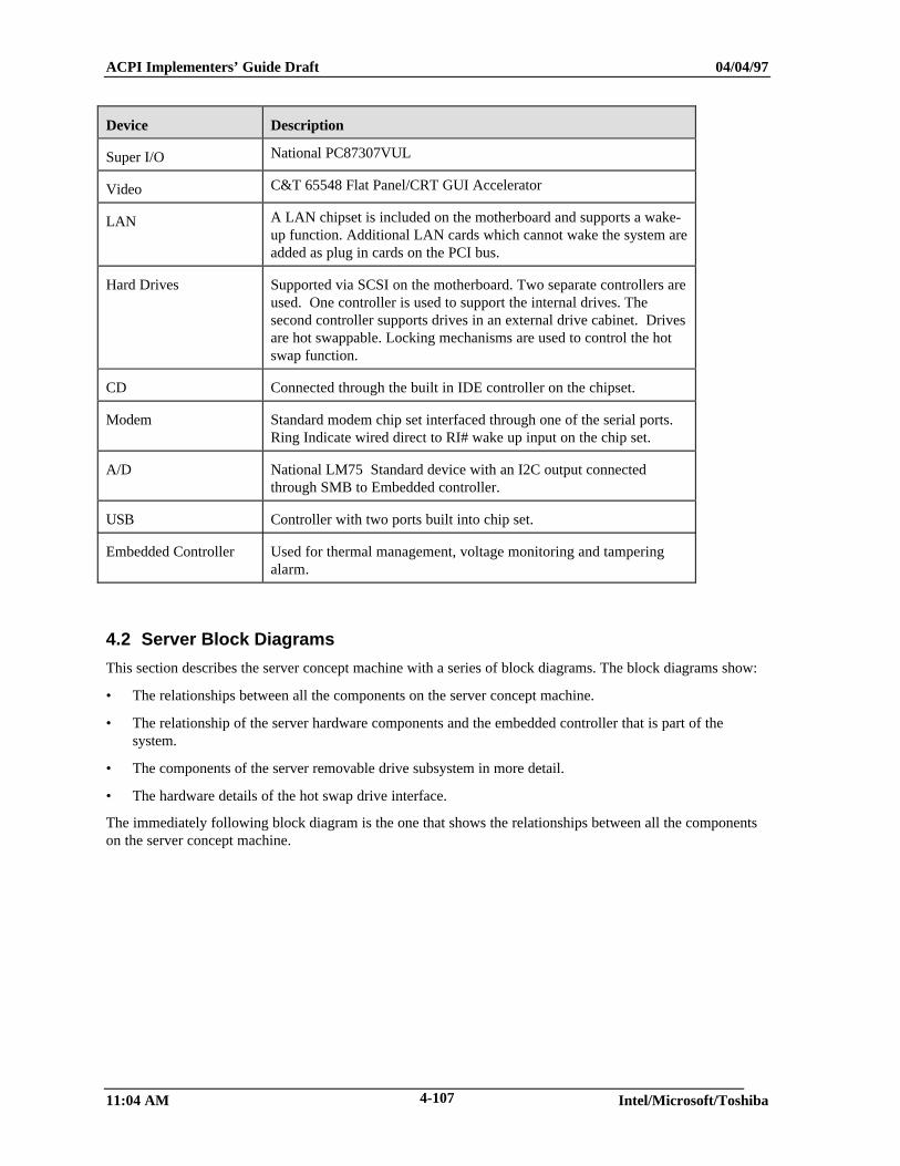
ACPI Implementers’ Guide Draft 04/04/97
11:04 AM Intel/Microsoft/Toshiba4-107
Device Description
Super I/O National PC87307VUL
Video C&T 65548 Flat Panel/CRT GUI Accelerator
LAN A LAN chipset is included on the motherboard and supports a wake-up function. Additional LAN cards which cannot wake the system areadded as plug in cards on the PCI bus.
Hard Drives Supported via SCSI on the motherboard. Two separate controllers areused. One controller is used to support the internal drives. Thesecond controller supports drives in an external drive cabinet. Drivesare hot swappable. Locking mechanisms are used to control the hotswap function.
CD Connected through the built in IDE controller on the chipset.
Modem Standard modem chip set interfaced through one of the serial ports.Ring Indicate wired direct to RI# wake up input on the chip set.
A/D National LM75 Standard device with an I2C output connectedthrough SMB to Embedded controller.
USB Controller with two ports built into chip set.
Embedded Controller Used for thermal management, voltage monitoring and tamperingalarm.
4.2 Server Block Diagrams
This section describes the server concept machine with a series of block diagrams. The block diagrams show:
• The relationships between all the components on the server concept machine.
• The relationship of the server hardware components and the embedded controller that is part of thesystem.
• The components of the server removable drive subsystem in more detail.
• The hardware details of the hot swap drive interface.
The immediately following block diagram is the one that shows the relationships between all the componentson the server concept machine.
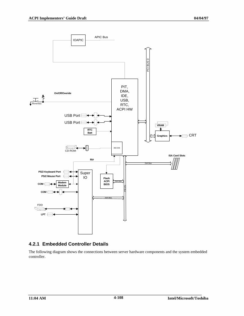
ACPI Implementers’ Guide Draft 04/04/97
11:04 AM Intel/Microsoft/Toshiba4-108
PIT,DMA,IDE,USB,RTC,
ACPI HW
FlashACPIBIOS
SuperIO
PS/2 Keyboard Port
PS/2 Mouse Port
LPT
COM
USB Port
USB Port
BM IDE
FDD
ISA
Bus
ISA Bus
ISA Bus
On/Off/Overide
ISA Card Slots
RTCBatt
RI#
ISA Bus
COM ModemModule
P
CI B
US
0
Momentary
Graphics
VRAM
CRT
IOAPICAPIC Bus
CD-ROM
4.2.1 Embedded Controller Details
The following diagram shows the connections between server hardware components and the system embeddedcontroller.
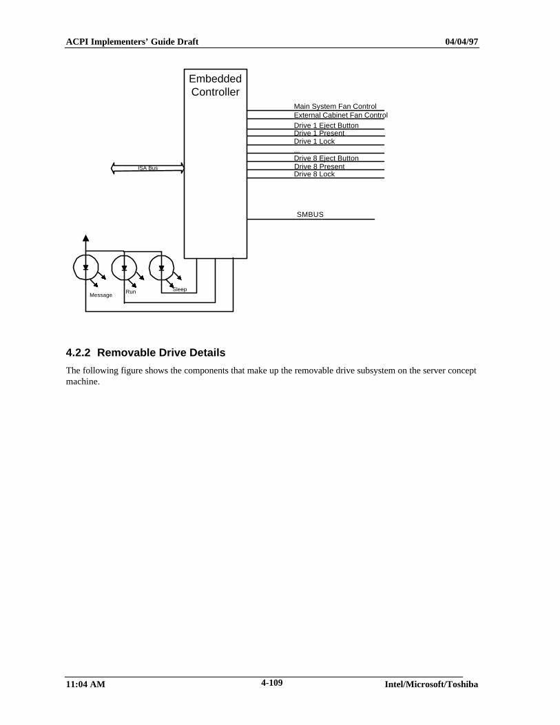
ACPI Implementers’ Guide Draft 04/04/97
11:04 AM Intel/Microsoft/Toshiba4-109
Sleep
EmbeddedController
Main System Fan ControlExternal Cabinet Fan ControlDrive 1 Eject ButtonDrive 1 PresentDrive 1 Lock...
Drive 8 Lock
Drive 8 Eject ButtonDrive 8 Present
SMBUS
MessageRun
ISA Bus
4.2.2 Removable Drive Details
The following figure shows the components that make up the removable drive subsystem on the server conceptmachine.
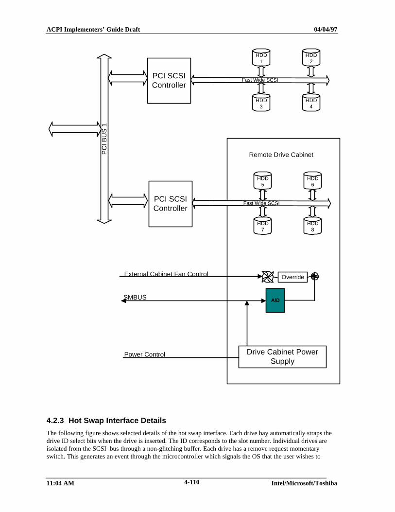
ACPI Implementers’ Guide Draft 04/04/97
11:04 AM Intel/Microsoft/Toshiba4-110
Remote Drive Cabinet
HDD1
HDD2
HDD3
HDD4
Fast Wide SCSIPCI SCSIController
HDD5
HDD6
HDD7
HDD8
Fast Wide SCSIPCI SCSIController
PC
I BU
S 1
SMBUS A/D
Drive Cabinet PowerSupply
Power Control
External Cabinet Fan Control Override
4.2.3 Hot Swap Interface Details
The following figure shows selected details of the hot swap interface. Each drive bay automatically straps thedrive ID select bits when the drive is inserted. The ID corresponds to the slot number. Individual drives areisolated from the SCSI bus through a non-glitching buffer. Each drive has a remove request momentaryswitch. This generates an event through the microcontroller which signals the OS that the user wishes to

ACPI Implementers’ Guide Draft 04/04/97
11:04 AM Intel/Microsoft/Toshiba4-111
remove a drive. A mechanical lock mechanism prevents removal of a drive until the OS acknowledges that itis ready through the microcontroller. An indicator shows when the lock has been released.
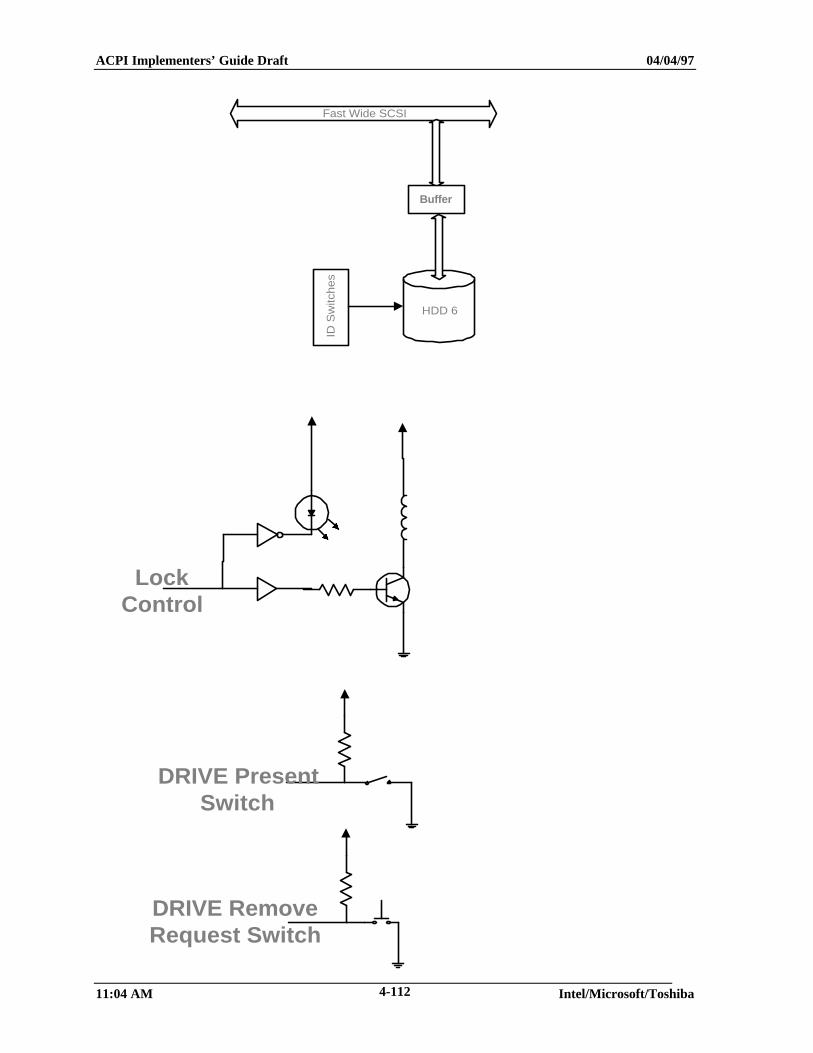
ACPI Implementers’ Guide Draft 04/04/97
11:04 AM Intel/Microsoft/Toshiba4-112
HDD 6
Fast Wide SCSI
Buffer
ID S
witc
hes
LockControl
DRIVE PresentSwitch
DRIVE RemoveRequest Switch
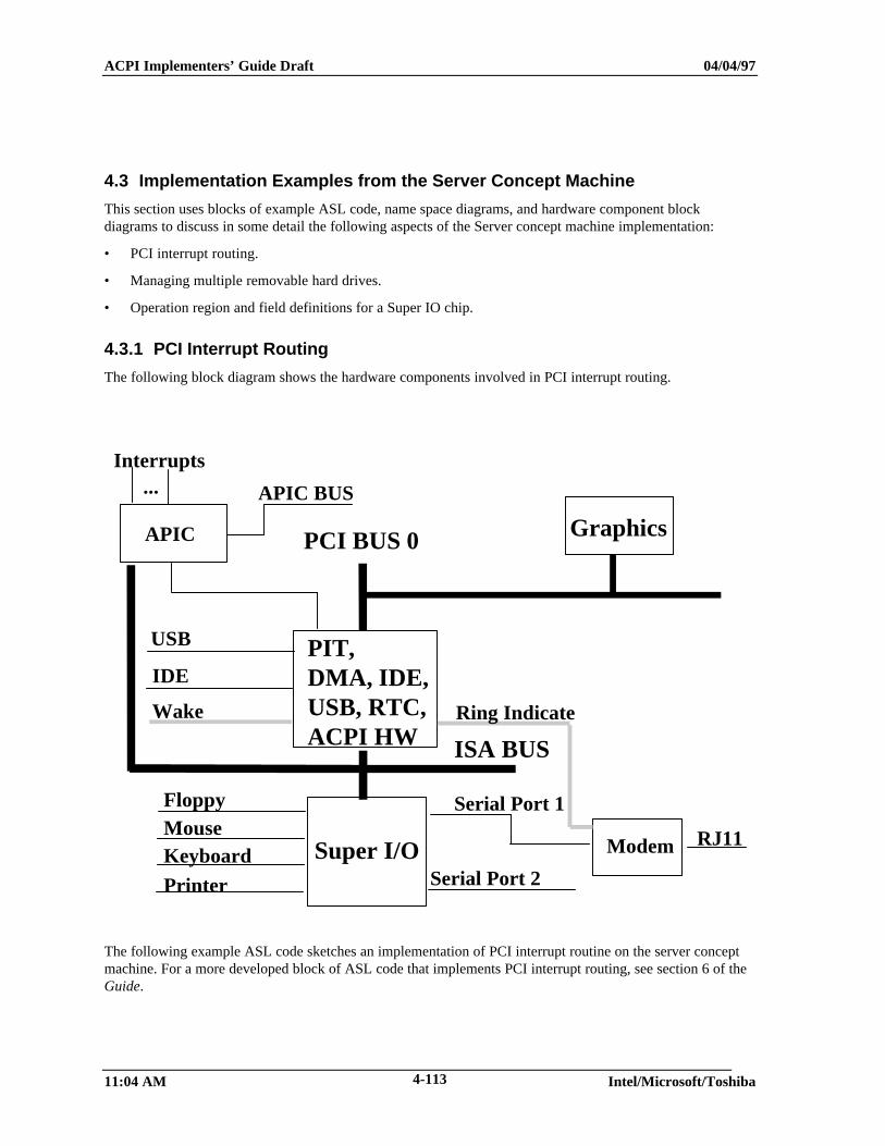
ACPI Implementers’ Guide Draft 04/04/97
11:04 AM Intel/Microsoft/Toshiba4-113
4.3 Implementation Examples from the Server Concept Machine
This section uses blocks of example ASL code, name space diagrams, and hardware component blockdiagrams to discuss in some detail the following aspects of the Server concept machine implementation:
• PCI interrupt routing.
• Managing multiple removable hard drives.
• Operation region and field definitions for a Super IO chip.
4.3.1 PCI Interrupt Routing
The following block diagram shows the hardware components involved in PCI interrupt routing.
PIT,DMA, IDE,USB, RTC,ACPI HW
PCI BUS 0
Super I/O
Graphics
ISA BUS
USB
IDE
Printer
FloppyMouseKeyboard
Serial Port 2
Serial Port 1
Modem RJ11
Ring IndicateWake
APIC
APIC BUS...Interrupts
The following example ASL code sketches an implementation of PCI interrupt routine on the server conceptmachine. For a more developed block of ASL code that implements PCI interrupt routing, see section 6 of theGuide.
ACPI Implementers’ Guide Draft 04/04/97
11:04 AM Intel/Microsoft/Toshiba4-114
Scope(\_SB) { // Start of _SB...
Device(LNKA){Name(_HID, EISAID("PNP0C0F")) // PCI interrupt linkName(_UID, 1)Name(_PRS, ResourceTemplate(){
Interrupt(ResourceProducer,...) {10,11} // IRQs 10,11})Method(_DIS) {...}Method(_CRS) {...}Method(_SRS, 1) {...}
}Device(LNKB){
Name(_HID, EISAID("PNP0C0F")) // PCI interrupt linkName(_UID, 2)Name(_PRS, ResourceTemplate(){
Interrupt(ResourceProducer,...) {11,12} // IRQs 11,12})Method(_DIS) {...}Method(_CRS) {...}Method(_SRS, 1) {...}
}Device(LNKC){
Name(_HID, EISAID("PNP0C0F")) // PCI interrupt linkName(_UID, 3)Name(_PRS, ResourceTemplate(){
Interrupt(ResourceProducer,...) {12,13} // IRQs 12,13})Method(_DIS) {...}Method(_CRS) {...}Method(_SRS, 1) {...}
}Device(LNKD){
Name(_HID, EISAID("PNP0C0F")) // PCI interrupt linkName(_UID, 4)Name(_PRS, ResourceTemplate(){
Interrupt(ResourceProducer,...) {13,14} // IRQs 13,14})Method(_DIS) {...}Method(_CRS) {...}Method(_SRS, 1) {...}
}
Device(PCI0) { // Root PCI Bus...Name(_PRT, Package{
Package{0x0004ffff, 0, LNKA, 0}, // Slot 1, INTAPackage{0x0004ffff, 1, LNKB, 0}, // Slot 1, INTBPackage{0x0004ffff, 2, LNKC, 0}, // Slot 1, INTCPackage{0x0004ffff, 3, LNKD, 0}, // Slot 1, INTDPackage{0x0005ffff, 0, LNKB, 0}, // Slot 2, INTAPackage{0x0005ffff, 1, LNKC, 0}, // Slot 2, INTBPackage{0x0005ffff, 2, LNKD, 0}, // Slot 2, INTCPackage{0x0006ffff, 3, LNKA, 0}, // Slot 2, INTDPackage{0x0006ffff, 0, LNKC, 0}, // Slot 3, INTAPackage{0x0006ffff, 1, LNKD, 0}, // Slot 3, INTBPackage{0x0006ffff, 2, LNKA, 0}, // Slot 3, INTCPackage{0x0006ffff, 3, LNKB, 0}, // Slot 3, INTD
})}
4.3.2 Managing Multiple Removable Hard Drives
This section walks through the parts of the server ACPI name space that contain objects used to managemultiple removable hard drives and the ASL code these objects contain. For information about the hardwarecomponents involved in managing multiple removable hard drives, see an earlier section.

ACPI Implementers’ Guide Draft 04/04/97
11:04 AM Intel/Microsoft/Toshiba4-115
4.3.3 Operation Region and Field Declarations for a Super I/O Chip
The National Super I/O chip registers are read and written through two levels of indirection. The ASLlanguage OperationRegion, Field, and BankField terms can be declared in combination to define this three-tier register arrangement, assigning field names to the working registers of interest. Once this declaration ismade, simple Store terms can be used to read from and write to the field names and the ACPI run-timecomponent built into the OS automatically takes care of all the details of managing the levels of indirection.
For example, the block of ASL code that declares field names for the National Super I/O chip workingregisters is shown below.
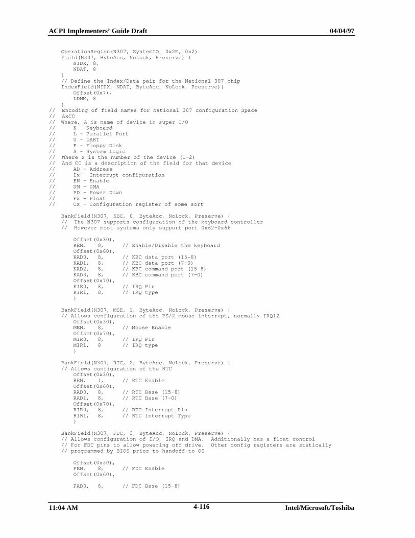
ACPI Implementers’ Guide Draft 04/04/97
11:04 AM Intel/Microsoft/Toshiba4-116
OperationRegion(N307, SystemIO, 0x2E, 0x2)Field(N307, ByteAcc, NoLock, Preserve) {
NIDX, 8,NDAT, 8
}// Define the Index/Data pair for the National 307 chipIndexField(NIDX, NDAT, ByteAcc, NoLock, Preserve){
Offset(0x7),LDNM, 8
}// Encoding of field names for National 307 configuration Space// AxCC// Where, A is name of device in super I/O// K - Keyboard// L - Parallel Port// U - UART// F - Floppy Disk// S - System Logic// Where x is the number of the device (1-2)// And CC is a description of the field for that device// AD - Address// Ix - Interrupt configuration// EN - Enable// DM - DMA// PD - Power Down// Fx - Float// Cx - Configuration register of some sort
BankField(N307, KBC, 0, ByteAcc, NoLock, Preserve) {// The N307 supports configuration of the keyboard controller// However most systems only support port 0x62-0x66
Offset(0x30),KEN, 8, // Enable/Disable the keyboardOffset(0x60),KAD0, 8, // KBC data port (15-8)KAD1, 8, // KBC data port (7-0)KAD2, 8, // KBC command port (15-8)KAD3, 8, // KBC command port (7-0)Offset(0x70),KIR0, 8, // IRQ PinKIR1, 8, // IRQ type}
BankField(N307, MSE, 1, ByteAcc, NoLock, Preserve) {// Allows configuration of the PS/2 mouse interrupt, normally IRQ12
Offset(0x30),MEN, 8, // Mouse EnableOffset(0x70),MIR0, 8, // IRQ PinMIR1, 8 // IRQ type}
BankField(N307, RTC, 2, ByteAcc, NoLock, Preserve) {// Allows configuration of the RTC
Offset(0x30),REN, 1, // RTC EnableOffset(0x60),RAD0, 8, // RTC Base (15-8)RAD1, 8, // RTC Base (7-0)Offset(0x70),RIR0, 8, // RTC Interrupt PinRIR1, 8, // RTC Interrupt Type}
BankField(N307, FDC, 3, ByteAcc, NoLock, Preserve) {// Allows configuration of I/O, IRQ and DMA. Additionally has a float control// For FDC pins to allow powering off drive. Other config registers are statically// programmed by BIOS prior to handoff to OS
Offset(0x30),FEN, 8, // FDC EnableOffset(0x60),
FAD0, 8, // FDC Base (15-8)
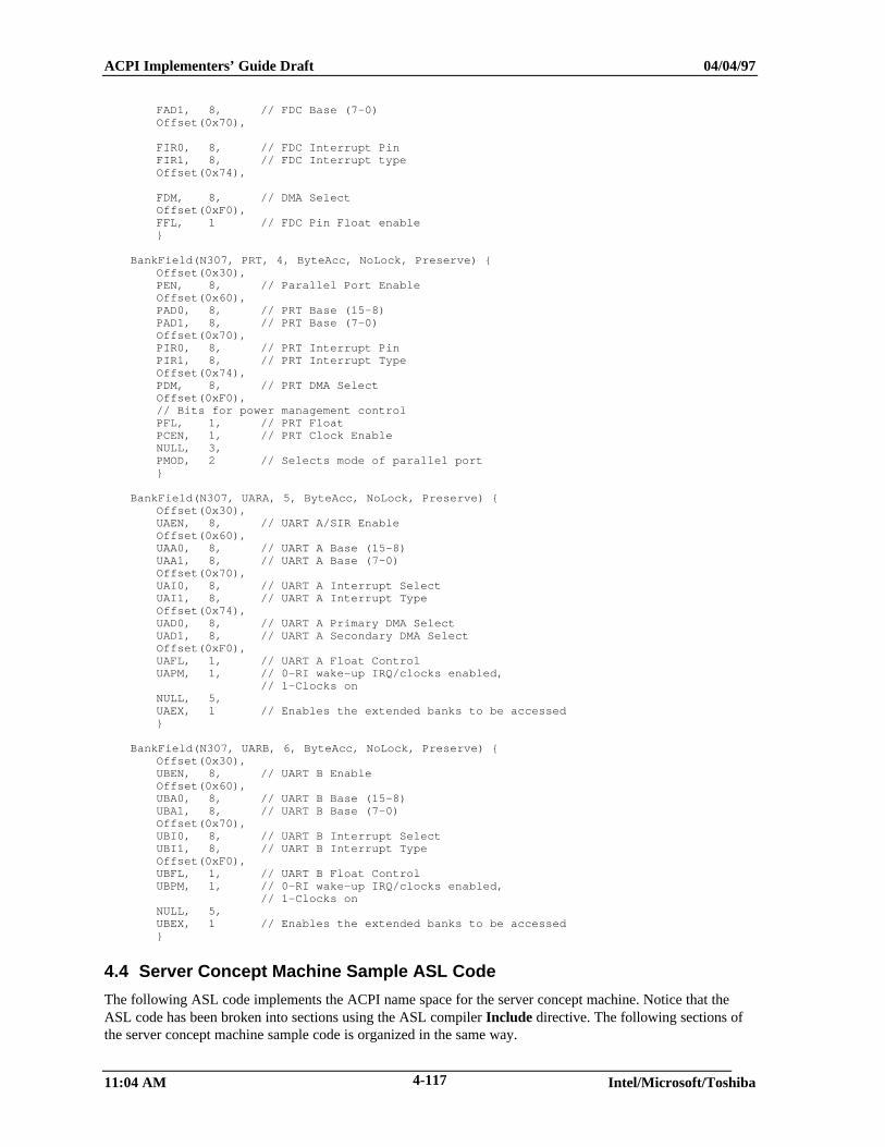
ACPI Implementers’ Guide Draft 04/04/97
11:04 AM Intel/Microsoft/Toshiba4-117
FAD1, 8, // FDC Base (7-0)Offset(0x70),
FIR0, 8, // FDC Interrupt PinFIR1, 8, // FDC Interrupt typeOffset(0x74),
FDM, 8, // DMA SelectOffset(0xF0),FFL, 1 // FDC Pin Float enable}
BankField(N307, PRT, 4, ByteAcc, NoLock, Preserve) {Offset(0x30),PEN, 8, // Parallel Port EnableOffset(0x60),PAD0, 8, // PRT Base (15-8)PAD1, 8, // PRT Base (7-0)Offset(0x70),PIR0, 8, // PRT Interrupt PinPIR1, 8, // PRT Interrupt TypeOffset(0x74),PDM, 8, // PRT DMA SelectOffset(0xF0),// Bits for power management controlPFL, 1, // PRT FloatPCEN, 1, // PRT Clock EnableNULL, 3,PMOD, 2 // Selects mode of parallel port}
BankField(N307, UARA, 5, ByteAcc, NoLock, Preserve) {Offset(0x30),UAEN, 8, // UART A/SIR EnableOffset(0x60),UAA0, 8, // UART A Base (15-8)UAA1, 8, // UART A Base (7-0)Offset(0x70),UAI0, 8, // UART A Interrupt SelectUAI1, 8, // UART A Interrupt TypeOffset(0x74),UAD0, 8, // UART A Primary DMA SelectUAD1, 8, // UART A Secondary DMA SelectOffset(0xF0),UAFL, 1, // UART A Float ControlUAPM, 1, // 0-RI wake-up IRQ/clocks enabled,
// 1-Clocks onNULL, 5,UAEX, 1 // Enables the extended banks to be accessed}
BankField(N307, UARB, 6, ByteAcc, NoLock, Preserve) {Offset(0x30),UBEN, 8, // UART B EnableOffset(0x60),UBA0, 8, // UART B Base (15-8)UBA1, 8, // UART B Base (7-0)Offset(0x70),UBI0, 8, // UART B Interrupt SelectUBI1, 8, // UART B Interrupt TypeOffset(0xF0),UBFL, 1, // UART B Float ControlUBPM, 1, // 0-RI wake-up IRQ/clocks enabled,
// 1-Clocks onNULL, 5,UBEX, 1 // Enables the extended banks to be accessed}
4.4 Server Concept Machine Sample ASL Code
The following ASL code implements the ACPI name space for the server concept machine. Notice that theASL code has been broken into sections using the ASL compiler Include directive. The following sections ofthe server concept machine sample code is organized in the same way.
ACPI Implementers’ Guide Draft 04/04/97
11:04 AM Intel/Microsoft/Toshiba4-118
4.5 Server Concept Machine ACPI Name Space
This section shows the ACPI name space and ASL code that creates that name space, based on the platformdesign illustrated in the previous section.
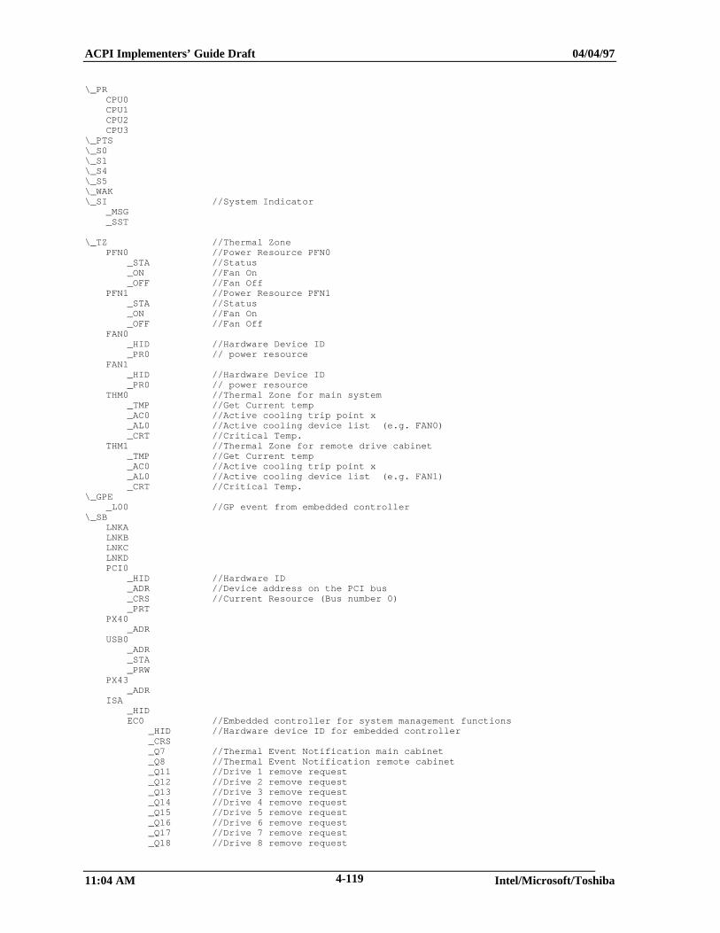
ACPI Implementers’ Guide Draft 04/04/97
11:04 AM Intel/Microsoft/Toshiba4-119
\_PRCPU0CPU1CPU2CPU3
\_PTS\_S0\_S1\_S4\_S5\_WAK\_SI //System Indicator
_MSG_SST
\_TZ //Thermal ZonePFN0 //Power Resource PFN0
_STA //Status_ON //Fan On_OFF //Fan Off
PFN1 //Power Resource PFN1_STA //Status_ON //Fan On_OFF //Fan Off
FAN0_HID //Hardware Device ID_PR0 // power resource
FAN1_HID //Hardware Device ID_PR0 // power resource
THM0 //Thermal Zone for main system_TMP //Get Current temp_AC0 //Active cooling trip point x_AL0 //Active cooling device list (e.g. FAN0)_CRT //Critical Temp.
THM1 //Thermal Zone for remote drive cabinet_TMP //Get Current temp_AC0 //Active cooling trip point x_AL0 //Active cooling device list (e.g. FAN1)_CRT //Critical Temp.
\_GPE_L00 //GP event from embedded controller
\_SBLNKALNKBLNKCLNKDPCI0
_HID //Hardware ID_ADR //Device address on the PCI bus_CRS //Current Resource (Bus number 0)_PRT
PX40_ADR
USB0_ADR_STA_PRW
PX43_ADR
ISA_HIDEC0 //Embedded controller for system management functions
_HID //Hardware device ID for embedded controller_CRS_Q7 //Thermal Event Notification main cabinet_Q8 //Thermal Event Notification remote cabinet_Q11 //Drive 1 remove request_Q12 //Drive 2 remove request_Q13 //Drive 3 remove request_Q14 //Drive 4 remove request_Q15 //Drive 5 remove request_Q16 //Drive 6 remove request_Q17 //Drive 7 remove request_Q18 //Drive 8 remove request
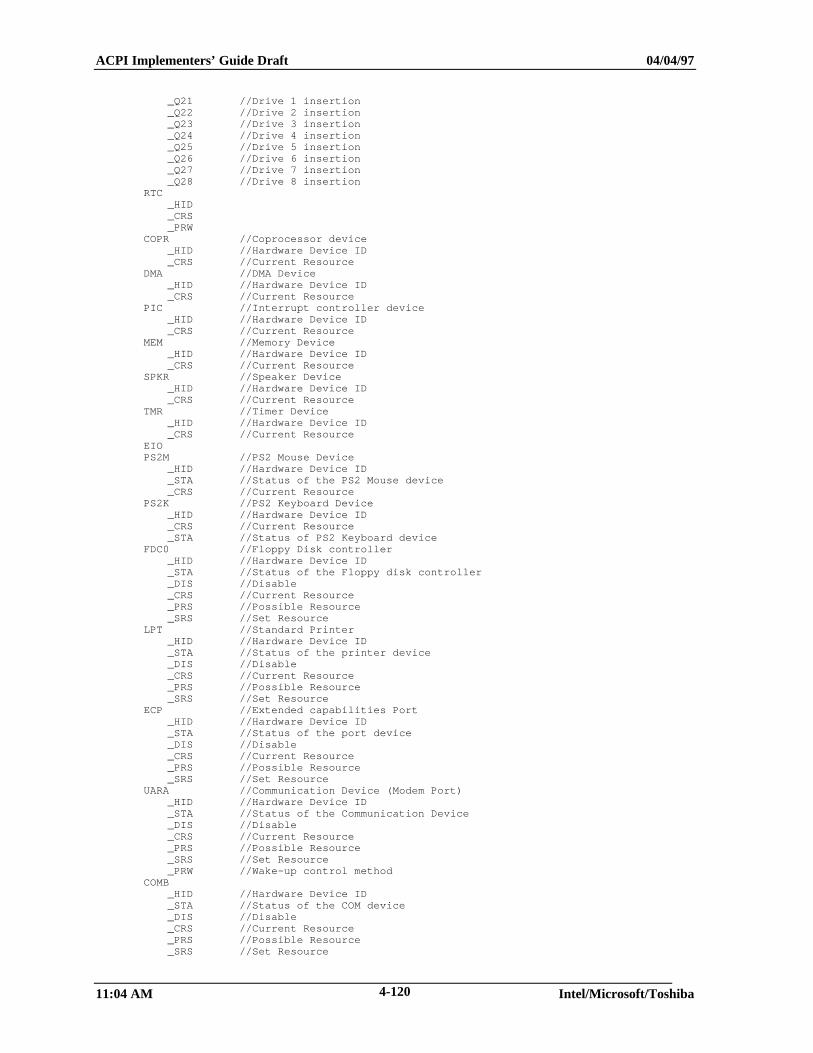
ACPI Implementers’ Guide Draft 04/04/97
11:04 AM Intel/Microsoft/Toshiba4-120
_Q21 //Drive 1 insertion_Q22 //Drive 2 insertion_Q23 //Drive 3 insertion_Q24 //Drive 4 insertion_Q25 //Drive 5 insertion_Q26 //Drive 6 insertion_Q27 //Drive 7 insertion_Q28 //Drive 8 insertion
RTC_HID_CRS_PRW
COPR //Coprocessor device_HID //Hardware Device ID_CRS //Current Resource
DMA //DMA Device_HID //Hardware Device ID_CRS //Current Resource
PIC //Interrupt controller device_HID //Hardware Device ID_CRS //Current Resource
MEM //Memory Device_HID //Hardware Device ID_CRS //Current Resource
SPKR //Speaker Device_HID //Hardware Device ID_CRS //Current Resource
TMR //Timer Device_HID //Hardware Device ID_CRS //Current Resource
EIOPS2M //PS2 Mouse Device
_HID //Hardware Device ID_STA //Status of the PS2 Mouse device_CRS //Current Resource
PS2K //PS2 Keyboard Device_HID //Hardware Device ID_CRS //Current Resource_STA //Status of PS2 Keyboard device
FDC0 //Floppy Disk controller_HID //Hardware Device ID_STA //Status of the Floppy disk controller_DIS //Disable_CRS //Current Resource_PRS //Possible Resource_SRS //Set Resource
LPT //Standard Printer_HID //Hardware Device ID_STA //Status of the printer device_DIS //Disable_CRS //Current Resource_PRS //Possible Resource_SRS //Set Resource
ECP //Extended capabilities Port_HID //Hardware Device ID_STA //Status of the port device_DIS //Disable_CRS //Current Resource_PRS //Possible Resource_SRS //Set Resource
UARA //Communication Device (Modem Port)_HID //Hardware Device ID_STA //Status of the Communication Device_DIS //Disable_CRS //Current Resource_PRS //Possible Resource_SRS //Set Resource_PRW //Wake-up control method
COMB_HID //Hardware Device ID_STA //Status of the COM device_DIS //Disable_CRS //Current Resource_PRS //Possible Resource_SRS //Set Resource
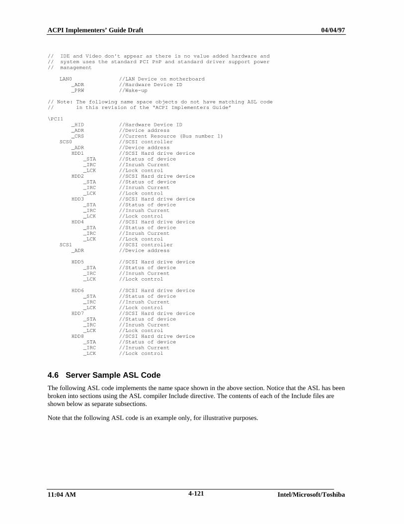
ACPI Implementers’ Guide Draft 04/04/97
11:04 AM Intel/Microsoft/Toshiba4-121
// IDE and Video don’t appear as there is no value added hardware and// system uses the standard PCI PnP and standard driver support power// management
LAN0 //LAN Device on motherboard_ADR //Hardware Device ID_PRW //Wake-up
// Note: The following name space objects do not have matching ASL code// in this revision of the “ACPI Implementers Guide”
\PCI1_HID //Hardware Device ID_ADR //Device address_CRS //Current Resource (Bus number 1)
SCS0 //SCSI controller_ADR //Device addressHDD1 //SCSI Hard drive device
_STA //Status of device_IRC //Inrush Current_LCK //Lock control
HDD2 //SCSI Hard drive device_STA //Status of device_IRC //Inrush Current_LCK //Lock control
HDD3 //SCSI Hard drive device_STA //Status of device_IRC //Inrush Current_LCK //Lock control
HDD4 //SCSI Hard drive device_STA //Status of device_IRC //Inrush Current_LCK //Lock control
SCS1 //SCSI controller_ADR //Device address
HDD5 //SCSI Hard drive device_STA //Status of device_IRC //Inrush Current_LCK //Lock control
HDD6 //SCSI Hard drive device_STA //Status of device_IRC //Inrush Current_LCK //Lock control
HDD7 //SCSI Hard drive device_STA //Status of device_IRC //Inrush Current_LCK //Lock control
HDD8 //SCSI Hard drive device_STA //Status of device_IRC //Inrush Current_LCK //Lock control
4.6 Server Sample ASL Code
The following ASL code implements the name space shown in the above section. Notice that the ASL has beenbroken into sections using the ASL compiler Include directive. The contents of each of the Include files areshown below as separate subsections.
Note that the following ASL code is an example only, for illustrative purposes.
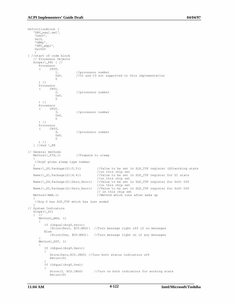
ACPI Implementers’ Guide Draft 04/04/97
11:04 AM Intel/Microsoft/Toshiba4-122
DefinitionBlock ( "SRV_exa1.aml",
"DSDT",0x10,"OEMy","SRV_xmpl",0x1000)
{ //start of code block // Processor Objects Scope(\_PR) { // Processor ( CPU0,
1, //processor number0x0, //C2 and C3 not supported in this implementation0
) {} Processor ( CPU1,
2, //processor number0x0,0
) {} Processor ( CPU2,
3, //processor number0x0,0
) {} Processor ( CPU3,
4, //processor number0x0,0
) {} } //end \_PR
// General methods Method(\_PTS,1) //Prepare to sleep {
//Arg0 gives sleep type number } Name(\_S0,Package(2){5,5}) //Value to be set in SLP_TYP register (S0)working state
//on this chip set Name(\_S1,Package(2){4,4}) //Value to be set in SLP_TYP register for S1 state
//on this chip set Name(\_S4,Package(2){Zero,Zero}) //Value to be set in SLP_TYP register for Soft Off
//on this chip set Name(\_S5,Package(2){Zero,Zero}) //Value to be set in SLP_TYP register for Soft Off
// on this chip set Method(\WAK,1) //Method which runs after wake up {
//Arg 0 has SLP_TYP which has just ended }// System Indicators Scope(\_SI) { // Method(_MSG, 1) { If (LEqual(Arg0,Zero)) {Store(Zero, EC0.MSG)} //Turn message light off if no messages Else {Store(One, EC0.MSG)} //Turn message light on if any messages } Method(_SST, 1) { If (LEqual(Arg0,Zero)) { Store(Zero,EC0.IND0) //Turn both status indicators off Return(0) } If (LEqual(Arg0,One)) { Store(3, EC0.IND0) //Turn on both indicators for working state Return(0)
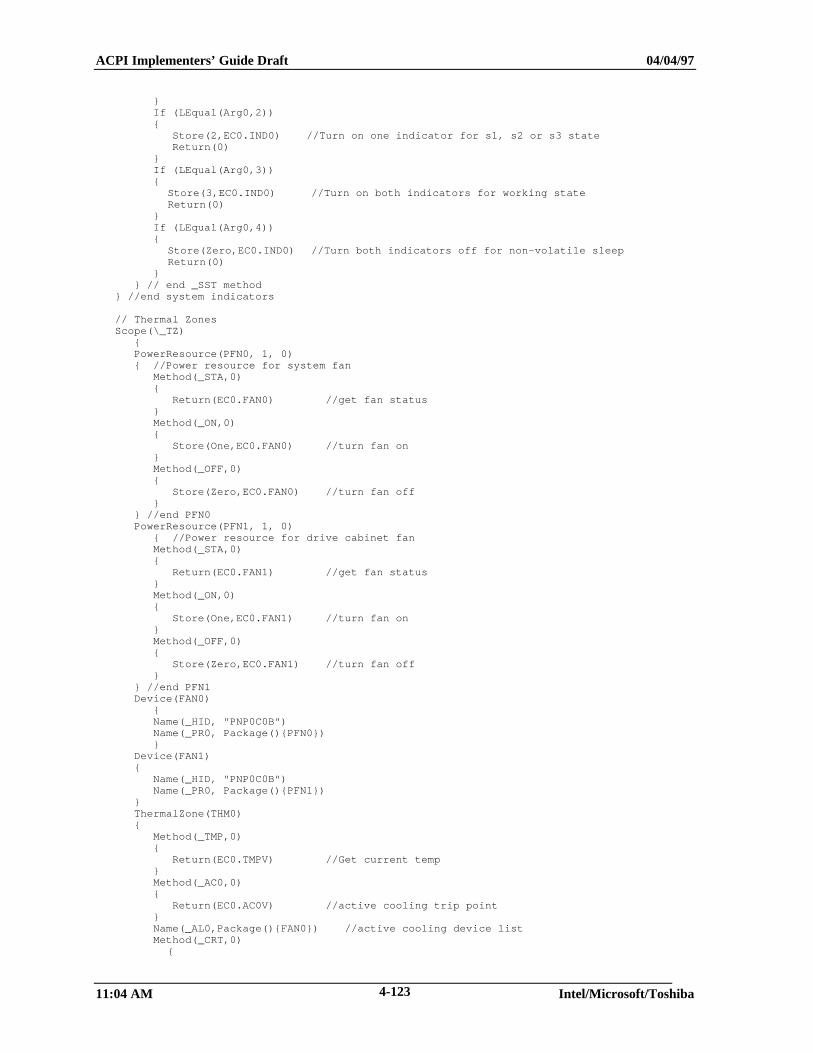
ACPI Implementers’ Guide Draft 04/04/97
11:04 AM Intel/Microsoft/Toshiba4-123
} If (LEqual(Arg0,2)) { Store(2,EC0.IND0) //Turn on one indicator for s1, s2 or s3 state Return(0) } If (LEqual(Arg0,3)) {
Store(3,EC0.IND0) //Turn on both indicators for working stateReturn(0)
} If (LEqual(Arg0,4)) {
Store(Zero,EC0.IND0) //Turn both indicators off for non-volatile sleepReturn(0)
} } // end _SST method } //end system indicators
// Thermal Zones Scope(\_TZ) { PowerResource(PFN0, 1, 0) { //Power resource for system fan Method(_STA,0) { Return(EC0.FAN0) //get fan status } Method(_ON,0) { Store(One,EC0.FAN0) //turn fan on } Method(_OFF,0) { Store(Zero,EC0.FAN0) //turn fan off } } //end PFN0 PowerResource(PFN1, 1, 0) { //Power resource for drive cabinet fan Method(_STA,0) { Return(EC0.FAN1) //get fan status } Method(_ON,0) { Store(One,EC0.FAN1) //turn fan on } Method(_OFF,0) { Store(Zero,EC0.FAN1) //turn fan off } } //end PFN1 Device(FAN0) { Name(_HID, "PNP0C0B") Name(_PR0, Package(){PFN0}) } Device(FAN1) { Name(_HID, "PNP0C0B") Name(_PR0, Package(){PFN1}) } ThermalZone(THM0) { Method(_TMP,0) { Return(EC0.TMPV) //Get current temp } Method(_AC0,0) { Return(EC0.AC0V) //active cooling trip point } Name(_AL0,Package(){FAN0}) //active cooling device list Method(_CRT,0)
{
ACPI Implementers’ Guide Draft 04/04/97
11:04 AM Intel/Microsoft/Toshiba4-124
Return(EC0.CRTV) //Get critical temp trip point } } //end THM0 ThermalZone(THM1) { Method(_TMP,0) { Return(EC0.TMPR) //Get current temp } Method(_AC0,0) { Return(EC0.AC0R) //active cooling trip point //} } Name(_AL0,Package(){FAN1}) //active cooling device list Method(_CRT,0) { Return(EC0.CRTR) //Get critical temp trip point } } //end THM1 } //end thermal zones
Scope(\_GPE){ //Method(_L00) { //GP event handle to GP_STS.00
Notify(EC0,0) //EC event notification}
} //end general purpose events
Scope(\_SB) { //
Device(LNKA){Name(_HID, EISAID("PNP0C0F")) // PCI interrupt linkName(_UID, 1)
// Name(_PRS, ResourceTemplate(){// Interrupt(ResourceProducer,...) {10,11} // IRQs 10,11// })// Method(_DIS) {...}// Method(_CRS) {...}// Method(_SRS, 1) {...}
}Device(LNKB){
Name(_HID, EISAID("PNP0C0F")) // PCI interrupt link// Name(_UID, 2)// Name(_PRS, ResourceTemplate(){// Interrupt(ResourceProducer,...) {11,12} // IRQs 11,12// })// Method(_DIS) {...}// Method(_CRS) {...}// Method(_SRS, 1) {...}
}Device(LNKC){
Name(_HID, EISAID("PNP0C0F")) // PCI interrupt link// Name(_UID, 3)// Name(_PRS, ResourceTemplate(){// Interrupt(ResourceProducer,...) {12,13} // IRQs 12,13// })// Method(_DIS) {...}// Method(_CRS) {...}// Method(_SRS, 1) {...}
}Device(LNKD){
Name(_HID, EISAID("PNP0C0F")) // PCI interrupt link// Name(_UID, 4)// Name(_PRS, ResourceTemplate(){// Interrupt(ResourceProducer,...) {13,14} // IRQs 13,14// })// Method(_DIS) {...}// Method(_CRS) {...}// Method(_SRS, 1) {...}
}
Device(PCI0) { // Root PCI Bus Name(_HID, "PNP0A03") //Need _HID for root device
Name(_ADR,00000000) //Num(00000000))//Also need _ADR since this appears in PCI config space
ACPI Implementers’ Guide Draft 04/04/97
11:04 AM Intel/Microsoft/Toshiba4-125
//Dword constant with upper word=device number//lowerword = function
Method (_CRS,0){ //Current Resources for root bridge 0Return(Zero)
}
Name(_PRT, Package(){Package(){0x0004ffff, 0, LNKA, 0}, // Slot 1, INTAPackage(){0x0004ffff, 1, LNKB, 0}, // Slot 1, INTBPackage(){0x0004ffff, 2, LNKC, 0}, // Slot 1, INTCPackage(){0x0004ffff, 3, LNKD, 0}, // Slot 1, INTDPackage(){0x0005ffff, 0, LNKB, 0}, // Slot 2, INTAPackage(){0x0005ffff, 1, LNKC, 0}, // Slot 2, INTBPackage(){0x0005ffff, 2, LNKD, 0}, // Slot 2, INTCPackage(){0x0006ffff, 3, LNKA, 0}, // Slot 2, INTDPackage(){0x0006ffff, 0, LNKC, 0}, // Slot 3, INTAPackage(){0x0006ffff, 1, LNKD, 0}, // Slot 3, INTBPackage(){0x0006ffff, 2, LNKA, 0}, // Slot 3, INTCPackage(){0x0006ffff, 3, LNKB, 0}, // Slot 3, INTD
})
Device(PX40) { // Map f0 space Name(_ADR,0x00070000) //Address+function. Address is defined by //how chip is connected to PCI bus } //
// IDE doesn’t appear as there is no value added hardware and system// uses the standard PCI PnP and standard driver support power management
Device(USB0) { // Map f2 space, USB Host controllerName(_ADR, 0x00070002)OperationRegion(CFG2, PCI_Config, 0x0, 0x4)Field(CFG2,DWordAcc,NoLock,Preserve){
Offset(0x20),USBB,8} //USB Base address
Method(_STA,0) { //Status of the USB deviceAnd(USBB,0xFFE0,Local0) //get the device base addressIf (LEqual(Local0,Zero))
{Return(One)} //Return device present if no//Base address programmed
Else{Return(0x3)} //else return present and active
} //end _STA methodName(_PRW,Package()
{8, //Bit number in GPEx_EN to enable USB resume 1 //Reference to lowest sleeping state which can be
//entered while still providing wake functionality}
) } //end of USB device Device(PX43) { // Map f3 space
Name(_ADR, 0x00070003)OperationRegion(CFG3,PCI_Config,0x0,0x4) // Map PCI Config SpaceOperationRegion(GPOB,SystemIO,0xE0,4) // Operation Region for
//general purpose output pins//0xE0 is chosen for example only
Device(ISA) { //Name(_HID, "PNP0A00")Device(EC0){ //Embedded Controller
Name(_HID, "PNP0C09") //ID for embedded ControllerMethod(_CRS,0) { //Current Resource for EC
Name(ECBF, Buffer(144) //18 bytes{0x47, 0x01, 0x62, 0x00, 0x62, 0x00, 0x01, 0x01,0x47, 0x01, 0x66, 0x00, 0x66, 0x00, 0x01, 0x01,0x79, 0x00} //end Buffer
)Return(ECBF)
}OperationRegion(EC0, EmbeddedControl, 0, 0xFF)
Field(EC0, AnyAcc, Lock, Preserve){IND0,2,,6,FAN0,1, //Main Cabinet Fan
ACPI Implementers’ Guide Draft 04/04/97
11:04 AM Intel/Microsoft/Toshiba4-126
FAN1,1, //Remote Cabinet Fan,6, //skipsTMPV,8, //Main Cabinet temperatureAC0V,8, //Main cabinet active cooling trip pointCRTV,8, //Main cabinet critical ValueTMPR,8, //Slave Cabinet temperatureAC0R,8, //Slave cabinet active cooling trip pointCRTR,8, //Slave cabinet critical trip pointHD1L,1, //Hard Drive 1 LockHD1S,4, //Hard drive 1 StatusPS8,1, //Hard Drive 1 Power Status,2,
//...additional entries for drives 2-7
HD8L,1, //Hard Drive 8 LockHD8S,4, //Hard drive 8 StatusPS8,1, //Hard Drive 8 Power Status,2,RPWR,1, //Remote Cabinet Power ControlRPWS,1 //Remote Cabinet Power Status} //end Field
Method(_Q07){ //Thermal event for main CabinetNotify(\_TZ.THM0, 0x80)
}Method(_Q08){ //Thermal event for remote Cabinet
Notify(\_TZ.THM1, 0x80)}Method(_Q11){ //Drive 1 remove request
Notify(\_SB.PCI1.SCS0.HDD1, 0x1) //Notify OS of//User request to eject HDD1
}
//...additional event entries for drives 2-7
Method(_Q18){ //Drive 8 remove requestNotify(\_SB.PCI1.SCS8.HDD8, 0x1) //Notify OS of
// user request to eject HDD8}Method(_Q21){ //Drive 1 insert
Notify(\_SB.PCI1.SCS0.HDD1, 0x0) //Device //check notify
}
//...additional event entries for drives 2-7
Method(_Q28){ //Drive 8 insertNotify(\_SB.PCI1.SCS1.HDD8, 0x0) //Device
//check notify}
} //end EC device Device(RTC) { //Real Time Clock Device
Name(_HID, "PNP0B00") //Hardware Device IDMethod(_CRS,0) { //Current Resource
Name(RTCB,Buffer(104) //13 bytes{0x47, //IO descriptor0x0,0x70,0x00,0x70,0x00,0x0,0x4,0x22,0x0,0x1,0x79,0x0}
)Return(RTCB)
} //end _CRS method// Method(_PRW,0){
ACPI Implementers’ Guide Draft 04/04/97
11:04 AM Intel/Microsoft/Toshiba4-127
// }// ACPI assumes RTC can wake system from S1-S5
} // end RTC deviceInclude("Coproc.asl")Include("DMA.asl")Include("INTR.asl")Include("Memory.asl")Include("Spkr.asl")Include("Timer.asl")
Include("N307.asl")//Pcode for National 307 super IO
} // end of ISA device} // end of PX43 device
// Video doesn’t appear as a Device object in the ACPI name space// because there is no value-added hardware and system// uses the standard PCI PnP and standard driver support power management
Device(LAN0){ //LAN deviceName(_ADR, 0x00060000) //Device address on the PCI busName(_PRW,Package(){
11, //Wake-up. Chip set's LID bit//used to cause a wake event since//LID would not otherwise be used.
1 //Reference to lowest sleeping state where//wake functionality can be supported
})
//Additional LAN controllers may be added but only the onboard LAN controller has the//value added wake function. } // end LAN0 } // End of PCI 0 Bus
Device(PCI1) { // Root PCI BusName(_HID, "PNP0A03") //Need _HID for root deviceName(_ADR,0x00010000) //Also need _ADR since this appears in PCI config space
//Dword constant with upper word=device number//lowerword = function
Method (_CRS,0){ //Current Resources for root bridge 1Return(One)}
Name(_PRT, Package(){Package(){0x0004ffff, 0, LNKA, 0}, // Slot 1, INTAPackage(){0x0004ffff, 1, LNKB, 0}, // Slot 1, INTBPackage(){0x0004ffff, 2, LNKC, 0}, // Slot 1, INTCPackage(){0x0004ffff, 3, LNKD, 0}, // Slot 1, INTDPackage(){0x0005ffff, 0, LNKB, 0}, // Slot 2, INTAPackage(){0x0005ffff, 1, LNKC, 0}, // Slot 2, INTBPackage(){0x0005ffff, 2, LNKD, 0}, // Slot 2, INTCPackage(){0x0006ffff, 3, LNKA, 0}, // Slot 2, INTDPackage(){0x0006ffff, 0, LNKC, 0}, // Slot 3, INTAPackage(){0x0006ffff, 1, LNKD, 0}, // Slot 3, INTBPackage(){0x0006ffff, 2, LNKA, 0}, // Slot 3, INTCPackage(){0x0006ffff, 3, LNKB, 0}, // Slot 3, INTD
})
Device(SCS0){ //Fast wide SCSI deviceName(_ADR, 0x00060000) //Device address on the PCI busDevice(HDD1){
Name(_ADR, 0x01) //Drive's ID on SCSI busMethod(_STA,0){
Return(EC0.HD1S) //Return Status of Drive//Bit 0=Present if set//Bit 1=Enabled//Bit 2=Show in user interface//Bit 3=Device is functioning properly
}Name(_IRC,Zero)Method(_LCK,1)
{Store(Arg0,EC0.HD1L) //Lock or unlock drive}
} //end HDD1
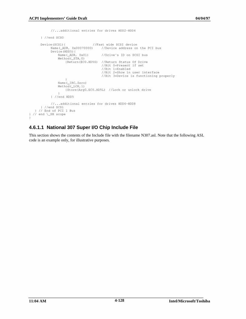
ACPI Implementers’ Guide Draft 04/04/97
11:04 AM Intel/Microsoft/Toshiba4-128
//...additional entries for drives HDD2-HDD4
} //end SCS0
Device(SCS1){ //Fast wide SCSI deviceName(_ADR, 0x00070000) //Device address on the PCI busDevice(HDD5){
Name(_ADR, 0x01) //Drive's ID on SCSI busMethod(_STA,0)
{Return(EC0.HD5S) //Return Status Of Drive//Bit 0=Present if set//Bit 1=Enabled//Bit 2=Show in user interface//Bit 3=Device is functioning properly
}Name(_IRC,Zero)Method(_LCK,1)
{Store(Arg0,EC0.HD5L) //Lock or unlock drive}
} //end HDD5
//...additional entries for drives HDD6-HDD8 } //end SCS1 } // End of PCI 1 Bus} // end \_SB scope}
4.6.1.1 National 307 Super I/O Chip Include File
This section shows the contents of the Include file with the filename N307.asl. Note that the following ASLcode is an example only, for illustrative purposes.
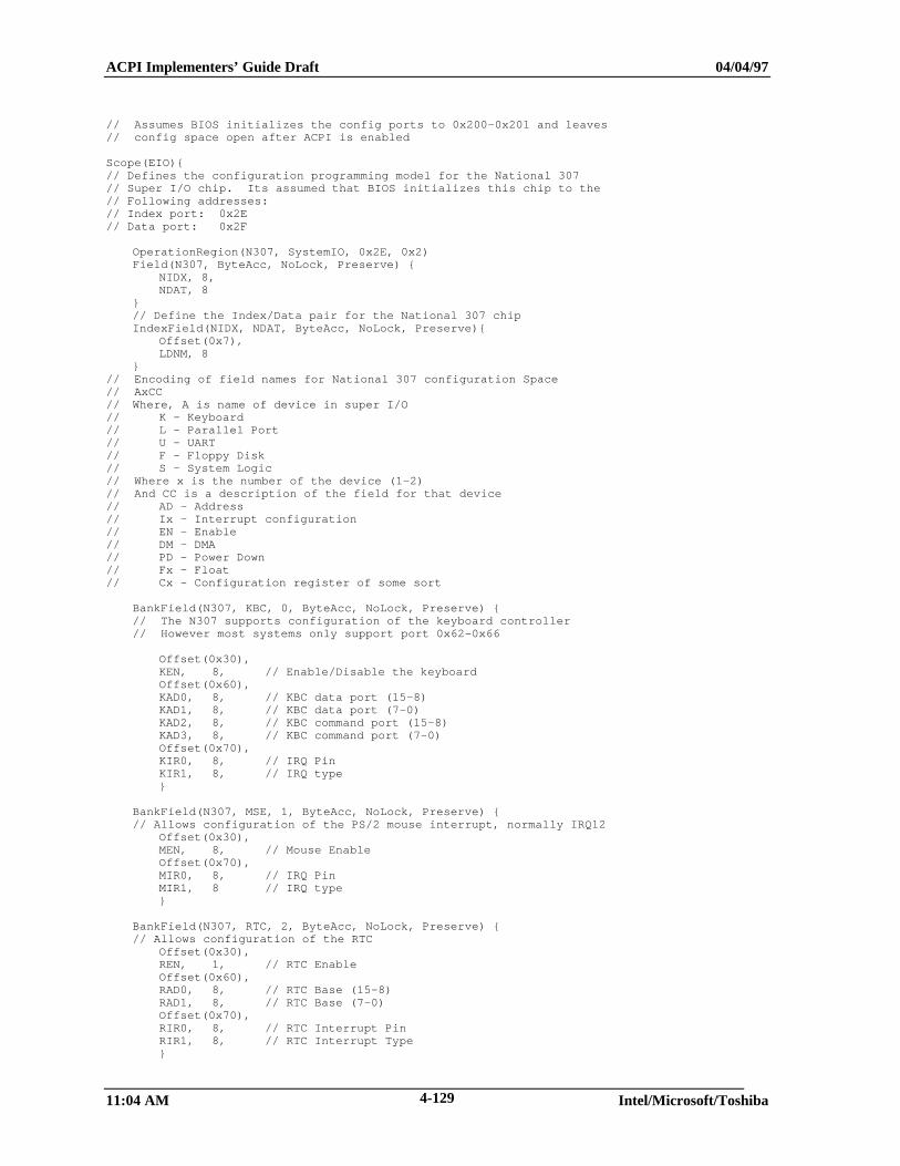
ACPI Implementers’ Guide Draft 04/04/97
11:04 AM Intel/Microsoft/Toshiba4-129
// Assumes BIOS initializes the config ports to 0x200-0x201 and leaves// config space open after ACPI is enabled
Scope(EIO){// Defines the configuration programming model for the National 307// Super I/O chip. Its assumed that BIOS initializes this chip to the// Following addresses:// Index port: 0x2E// Data port: 0x2F
OperationRegion(N307, SystemIO, 0x2E, 0x2)Field(N307, ByteAcc, NoLock, Preserve) {
NIDX, 8,NDAT, 8
}// Define the Index/Data pair for the National 307 chipIndexField(NIDX, NDAT, ByteAcc, NoLock, Preserve){
Offset(0x7),LDNM, 8
}// Encoding of field names for National 307 configuration Space// AxCC// Where, A is name of device in super I/O// K - Keyboard// L - Parallel Port// U - UART// F - Floppy Disk// S - System Logic// Where x is the number of the device (1-2)// And CC is a description of the field for that device// AD - Address// Ix - Interrupt configuration// EN - Enable// DM - DMA// PD - Power Down// Fx - Float// Cx - Configuration register of some sort
BankField(N307, KBC, 0, ByteAcc, NoLock, Preserve) {// The N307 supports configuration of the keyboard controller// However most systems only support port 0x62-0x66
Offset(0x30),KEN, 8, // Enable/Disable the keyboardOffset(0x60),KAD0, 8, // KBC data port (15-8)KAD1, 8, // KBC data port (7-0)KAD2, 8, // KBC command port (15-8)KAD3, 8, // KBC command port (7-0)Offset(0x70),KIR0, 8, // IRQ PinKIR1, 8, // IRQ type}
BankField(N307, MSE, 1, ByteAcc, NoLock, Preserve) {// Allows configuration of the PS/2 mouse interrupt, normally IRQ12
Offset(0x30),MEN, 8, // Mouse EnableOffset(0x70),MIR0, 8, // IRQ PinMIR1, 8 // IRQ type}
BankField(N307, RTC, 2, ByteAcc, NoLock, Preserve) {// Allows configuration of the RTC
Offset(0x30),REN, 1, // RTC EnableOffset(0x60),RAD0, 8, // RTC Base (15-8)RAD1, 8, // RTC Base (7-0)Offset(0x70),RIR0, 8, // RTC Interrupt PinRIR1, 8, // RTC Interrupt Type}
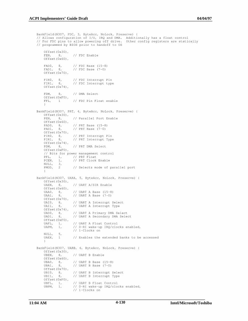
ACPI Implementers’ Guide Draft 04/04/97
11:04 AM Intel/Microsoft/Toshiba4-130
BankField(N307, FDC, 3, ByteAcc, NoLock, Preserve) {// Allows configuration of I/O, IRQ and DMA. Additionally has a float control// For FDC pins to allow powering off drive. Other config registers are statically// programmed by BIOS prior to handoff to OS
Offset(0x30),FEN, 8, // FDC EnableOffset(0x60),
FAD0, 8, // FDC Base (15-8)FAD1, 8, // FDC Base (7-0)Offset(0x70),
FIR0, 8, // FDC Interrupt PinFIR1, 8, // FDC Interrupt typeOffset(0x74),
FDM, 8, // DMA SelectOffset(0xF0),FFL, 1 // FDC Pin Float enable}
BankField(N307, PRT, 4, ByteAcc, NoLock, Preserve) {Offset(0x30),PEN, 8, // Parallel Port EnableOffset(0x60),PAD0, 8, // PRT Base (15-8)PAD1, 8, // PRT Base (7-0)Offset(0x70),PIR0, 8, // PRT Interrupt PinPIR1, 8, // PRT Interrupt TypeOffset(0x74),PDM, 8, // PRT DMA SelectOffset(0xF0),// Bits for power management controlPFL, 1, // PRT FloatPCEN, 1, // PRT Clock EnableNULL, 3,PMOD, 2 // Selects mode of parallel port}
BankField(N307, UARA, 5, ByteAcc, NoLock, Preserve) {Offset(0x30),UAEN, 8, // UART A/SIR EnableOffset(0x60),UAA0, 8, // UART A Base (15-8)UAA1, 8, // UART A Base (7-0)Offset(0x70),UAI0, 8, // UART A Interrupt SelectUAI1, 8, // UART A Interrupt TypeOffset(0x74),UAD0, 8, // UART A Primary DMA SelectUAD1, 8, // UART A Secondary DMA SelectOffset(0xF0),UAFL, 1, // UART A Float ControlUAPM, 1, // 0-RI wake-up IRQ/clocks enabled,
// 1-Clocks onNULL, 5,UAEX, 1 // Enables the extended banks to be accessed}
BankField(N307, UARB, 6, ByteAcc, NoLock, Preserve) {Offset(0x30),UBEN, 8, // UART B EnableOffset(0x60),UBA0, 8, // UART B Base (15-8)UBA1, 8, // UART B Base (7-0)Offset(0x70),UBI0, 8, // UART B Interrupt SelectUBI1, 8, // UART B Interrupt TypeOffset(0xF0),UBFL, 1, // UART B Float ControlUBPM, 1, // 0-RI wake-up IRQ/clocks enabled,
// 1-Clocks on
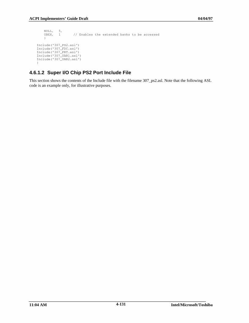
ACPI Implementers’ Guide Draft 04/04/97
11:04 AM Intel/Microsoft/Toshiba4-131
NULL, 5,UBEX, 1 // Enables the extended banks to be accessed}
Include("307_PS2.asl")Include("307_FDC.asl")Include("307_PRT.asl")Include("307_UAR1.asl")Include("307_UAR2.asl")}
4.6.1.2 Super I/O Chip PS2 Port Include File
This section shows the contents of the Include file with the filename 307_ps2.asl. Note that the following ASLcode is an example only, for illustrative purposes.
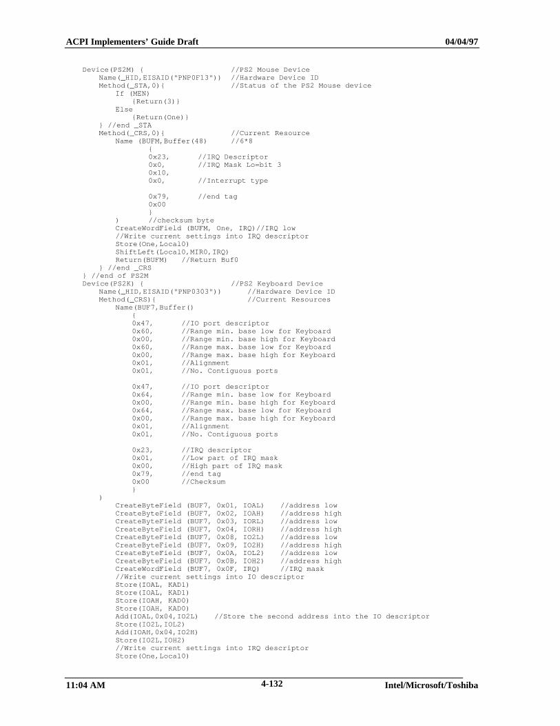
ACPI Implementers’ Guide Draft 04/04/97
11:04 AM Intel/Microsoft/Toshiba4-132
Device(PS2M) { //PS2 Mouse DeviceName(_HID,EISAID("PNP0F13")) //Hardware Device IDMethod(_STA,0){ //Status of the PS2 Mouse device
If (MEN){Return(3)}
Else{Return(One)}
} //end _STAMethod(_CRS,0){ //Current Resource
Name (BUFM,Buffer(48) //6*8{0x23, //IRQ Descriptor0x0, //IRQ Mask Lo=bit 30x10,0x0, //Interrupt type
0x79, //end tag0x00}
) //checksum byteCreateWordField (BUFM, One, IRQ)//IRQ low//Write current settings into IRQ descriptorStore(One,Local0)ShiftLeft(Local0,MIR0,IRQ)Return(BUFM) //Return Buf0
} //end _CRS} //end of PS2MDevice(PS2K) { //PS2 Keyboard Device
Name(_HID,EISAID("PNP0303")) //Hardware Device IDMethod(_CRS){ //Current Resources
Name(BUF7,Buffer(){0x47, //IO port descriptor0x60, //Range min. base low for Keyboard0x00, //Range min. base high for Keyboard0x60, //Range max. base low for Keyboard0x00, //Range max. base high for Keyboard0x01, //Alignment0x01, //No. Contiguous ports
0x47, //IO port descriptor0x64, //Range min. base low for Keyboard0x00, //Range min. base high for Keyboard0x64, //Range max. base low for Keyboard0x00, //Range max. base high for Keyboard0x01, //Alignment0x01, //No. Contiguous ports
0x23, //IRQ descriptor0x01, //Low part of IRQ mask0x00, //High part of IRQ mask0x79, //end tag0x00 //Checksum}
)CreateByteField (BUF7, 0x01, IOAL) //address lowCreateByteField (BUF7, 0x02, IOAH) //address highCreateByteField (BUF7, 0x03, IORL) //address lowCreateByteField (BUF7, 0x04, IORH) //address highCreateByteField (BUF7, 0x08, IO2L) //address lowCreateByteField (BUF7, 0x09, IO2H) //address highCreateByteField (BUF7, 0x0A, IOL2) //address lowCreateByteField (BUF7, 0x0B, IOH2) //address highCreateWordField (BUF7, 0x0F, IRQ) //IRQ mask//Write current settings into IO descriptorStore(IOAL, KAD1)Store(IOAL, KAD1)Store(IOAH, KAD0)Store(IOAH, KAD0)Add(IOAL,0x04,IO2L) //Store the second address into the IO descriptorStore(IO2L,IOL2)Add(IOAH,0x04,IO2H)Store(IO2L,IOH2)//Write current settings into IRQ descriptorStore(One,Local0)
ACPI Implementers’ Guide Draft 04/04/97
11:04 AM Intel/Microsoft/Toshiba4-133
ShiftLeft(Local0,KIR0,IRQ)Return(BUF7) //Return Buf7
} //end _CRSMethod(_STA,0){ //Status of the PS2 Keyboard device
If (KEN){Return(3)}
Else{Return(One)}
} //end _STA}//end of PS2K
4.6.1.3 Super I/O Chip Floppy Disk Controller Include File
This section shows the contents of the Include file with the filename 307_fdc.asl. Note that the following ASLcode is an example only, for illustrative purposes.
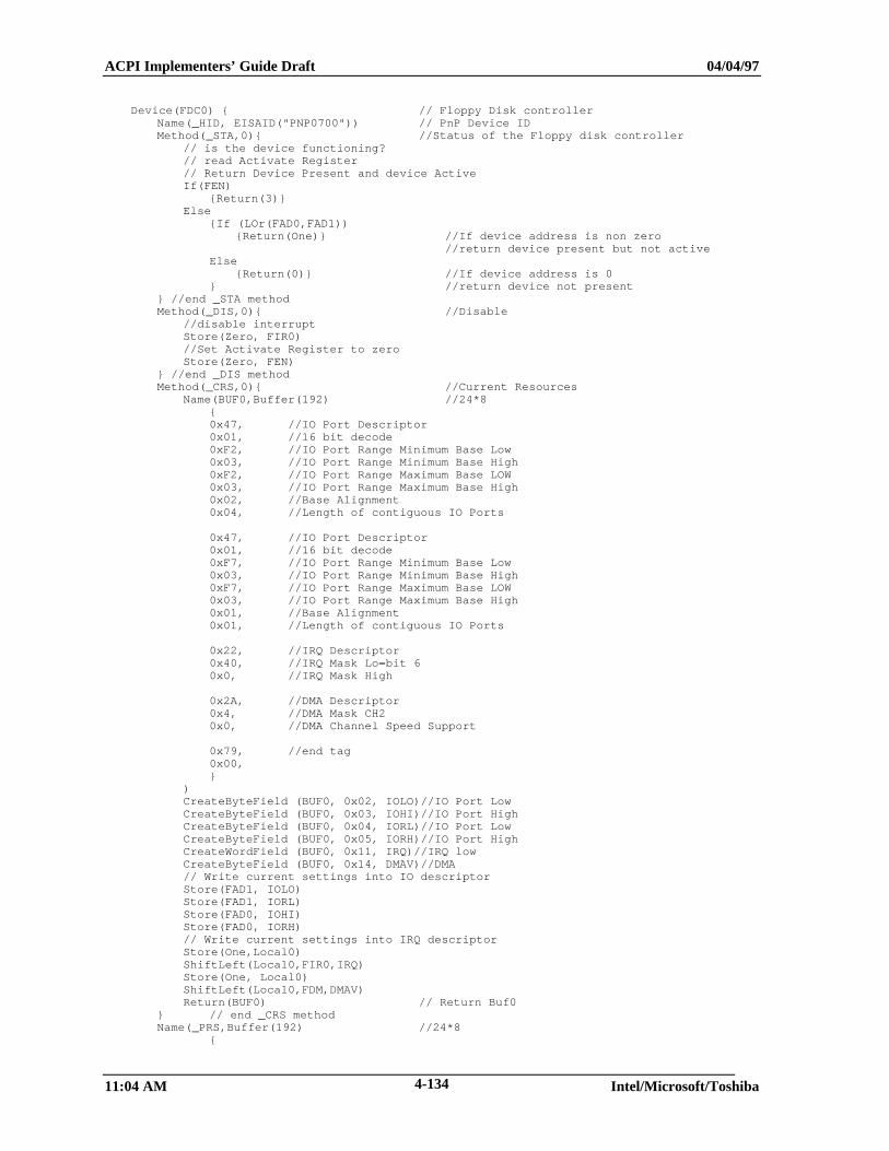
ACPI Implementers’ Guide Draft 04/04/97
11:04 AM Intel/Microsoft/Toshiba4-134
Device(FDC0) { // Floppy Disk controllerName(_HID, EISAID("PNP0700")) // PnP Device IDMethod(_STA,0){ //Status of the Floppy disk controller
// is the device functioning?// read Activate Register// Return Device Present and device ActiveIf(FEN)
{Return(3)}Else
{If (LOr(FAD0,FAD1)){Return(One)} //If device address is non zero
//return device present but not activeElse
{Return(0)} //If device address is 0} //return device not present
} //end _STA methodMethod(_DIS,0){ //Disable
//disable interruptStore(Zero, FIR0)//Set Activate Register to zeroStore(Zero, FEN)
} //end _DIS methodMethod(_CRS,0){ //Current Resources
Name(BUF0,Buffer(192) //24*8{0x47, //IO Port Descriptor0x01, //16 bit decode0xF2, //IO Port Range Minimum Base Low0x03, //IO Port Range Minimum Base High0xF2, //IO Port Range Maximum Base LOW0x03, //IO Port Range Maximum Base High0x02, //Base Alignment0x04, //Length of contiguous IO Ports
0x47, //IO Port Descriptor0x01, //16 bit decode0xF7, //IO Port Range Minimum Base Low0x03, //IO Port Range Minimum Base High0xF7, //IO Port Range Maximum Base LOW0x03, //IO Port Range Maximum Base High0x01, //Base Alignment0x01, //Length of contiguous IO Ports
0x22, //IRQ Descriptor0x40, //IRQ Mask Lo=bit 60x0, //IRQ Mask High
0x2A, //DMA Descriptor0x4, //DMA Mask CH20x0, //DMA Channel Speed Support
0x79, //end tag0x00,}
)CreateByteField (BUF0, 0x02, IOLO)//IO Port LowCreateByteField (BUF0, 0x03, IOHI)//IO Port HighCreateByteField (BUF0, 0x04, IORL)//IO Port LowCreateByteField (BUF0, 0x05, IORH)//IO Port HighCreateWordField (BUF0, 0x11, IRQ)//IRQ lowCreateByteField (BUF0, 0x14, DMAV)//DMA// Write current settings into IO descriptorStore(FAD1, IOLO)Store(FAD1, IORL)Store(FAD0, IOHI)Store(FAD0, IORH)// Write current settings into IRQ descriptorStore(One,Local0)ShiftLeft(Local0,FIR0,IRQ)Store(One, Local0)ShiftLeft(Local0,FDM,DMAV)Return(BUF0) // Return Buf0
} // end _CRS methodName(_PRS,Buffer(192) //24*8
{
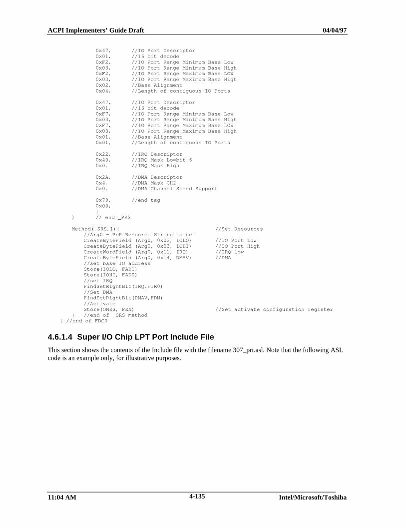
ACPI Implementers’ Guide Draft 04/04/97
11:04 AM Intel/Microsoft/Toshiba4-135
0x47, //IO Port Descriptor0x01, //16 bit decode0xF2, //IO Port Range Minimum Base Low0x03, //IO Port Range Minimum Base High0xF2, //IO Port Range Maximum Base LOW0x03, //IO Port Range Maximum Base High0x02, //Base Alignment0x04, //Length of contiguous IO Ports
0x47, //IO Port Descriptor0x01, //16 bit decode0xF7, //IO Port Range Minimum Base Low0x03, //IO Port Range Minimum Base High0xF7, //IO Port Range Maximum Base LOW0x03, //IO Port Range Maximum Base High0x01, //Base Alignment0x01, //Length of contiguous IO Ports
0x22, //IRQ Descriptor0x40, //IRQ Mask Lo=bit 60x0, //IRQ Mask High
0x2A, //DMA Descriptor0x4, //DMA Mask CH20x0, //DMA Channel Speed Support
0x79, //end tag0x00,}
) // end _PRS
Method(_SRS,1){ //Set Resources//Arg0 = PnP Resource String to setCreateByteField (Arg0, 0x02, IOLO) //IO Port LowCreateByteField (Arg0, 0x03, IOHI) //IO Port HighCreateWordField (Arg0, 0x11, IRQ) //IRQ lowCreateByteField (Arg0, 0x14, DMAV) //DMA//set base IO addressStore(IOLO, FAD1)Store(IOHI, FAD0)//set IRQFindSetRightBit(IRQ,FIR0)//Set DMAFindSetRightBit(DMAV,FDM)//ActivateStore(ONES, FEN) //Set activate configuration register
} //end of _SRS method} //end of FDC0
4.6.1.4 Super I/O Chip LPT Port Include File
This section shows the contents of the Include file with the filename 307_prt.asl. Note that the following ASLcode is an example only, for illustrative purposes.
ACPI Implementers’ Guide Draft 04/04/97
11:04 AM Intel/Microsoft/Toshiba4-136
// LPT DEVICEDevice(LPT) {
Name (_HID, EISAID("PNP0400")) // PnP ID for LPT PortMethod (_STA, 0) { // LPT Device Status
If(LEqual(PMOD, 0x1)){If (PEN)
{Return(3)} // Device present and activeElse
{Return(One)} // Present not active}Else
{Return(0)} // Not present} // End of _STA MethodMethod (_DIS) { // LPT Device Disable
Store (Zero, PIR0) // disable INTRStore (Zero, PEN) // Set Activate Reg = 0
} // end of _DIS method// LPT _CRS METHODMethod (_CRS) { // LPT Current Resources
Name(BUF5, Buffer () //13*8 Length of Buffer{0x47, // IO port descriptor0x01, // 16 bit decode0x78, // LPT1 @ 0x0278h0x02,0x78,0x02,0x08, // alignment0x08, // number of ports
0x22, // IRQ Descriptor0x80, // IRQ7 (Bit15=IRQ15....Bit0=IRQ0)0x00,
// No DMA
0x79, // end tag0x00,}
)//--------- Name the fields within the bufferCreateByteField (BUF5, 0x02, IOLO)CreateByteField (BUF5, 0x03, IOHI)CreateByteField (BUF5, 0x04, IORL) // IO Port LowCreateByteField (BUF5, 0x05, IORH) // IO Port HICreateWordField (BUF5, 0x09, IRQW)//--------- Read Devices PnP Config Regs into BufferStore(PAD1, IOLO) // Write IO Port LOW to dev cfg bufferStore(PAD1, IORL)Store(PAD0, IOHI) //Write IO Port High to dev cfg bufferStore(PAD0, IOAH)//---convert INTR(3:0) to single bit represetation of IRQStore(One,Local0)ShiftLeft(Local0,PIR0,IRQW) // (src, shiftcount, result)Return(BUF5) // return BUF3 filled with Current Resources
} // end _CRS method// LPT _PRS METHOD ---------------------------------------//--------- Create buffer with possible resources (pnp descriptor) ---------// Assume _PRS defines Resource Ordering [{IO,IRQ} vs {IRQ,IO}]// in _CRS & _SRS methodsName(_PRS, Buffer()
{ //13*80x30, // Start Dependent Function
0x47, // IO port descriptor0x01, // 16 bit decode0x78, // LPT1 @ 0x278h0x03,0x78,0x03,0x08, // alignment0x04, // number of ports
0x22, // IRQ Descriptor0x80, // IRQ7(Bit15=IRQ15....Bit0=IRQ0)0x00,
ACPI Implementers’ Guide Draft 04/04/97
11:04 AM Intel/Microsoft/Toshiba4-137
// No DMA0x38, // End Dependent Function
0x30, // Start Dependent Function
0x47, // IO port descriptor0x01, // 16 bit decode0x78, // LPT1 @ 0x278h0x02,0x78,0x02,
0x08, // alignment0x04, // number of ports
0x22, // IRQ Descriptor0xA0, // IRQ5 (Bit15=IRQ15....Bit0=IRQ0)0x00,
// No DMA0x38, // End Dependent Function0x30, // Start Dependent Function
0x47, // IO port descriptor0x01, // 16 bit decode0xBC, // LPT1 @ 0x278h0x03,0xBC,0x03,
0x08, // alignment0x04, // number of ports
0x22, // IRQ Descriptor0xA0, // IRQ5 (Bit15=IRQ15....Bit0=IRQ0)0x00,
// No DMA0x38, // End Dependent Function
0x79, //end tag0x00,
}) // end _PRS
// LPT _SRS METHOD -----------------------------------------------------
Method ( _SRS,1 ) { // LPT Set Resources & Enables the Device// ARG0 = PnP Resource String to Set// (IO,IRQ ordering assumed to be same as _PRS/_CRS)
// name the fields within the ARG0 String ---------------------
CreateByteField (ARG0, 0x02, IOLO) // IO Port LowCreateByteField (ARG0, 0x03, IOHI) // IO Port HICreateByteField (ARG0, 0x04, IORL) // IO Port LowCreateByteField (ARG0, 0x05, IORH) // IO Port HI
CreateWordField(ARG0, 0x06, IRQW) // IRQ MASK
STORE(IOLO, PAD1) // Write IO Port LOW to dev cfg regSTORE(IOHI, PAD0)
// Convert setbit position in IRQL:IRQH into 4bit field and write to PnP INTR regFindSetLeftBit(IRQW, PIR0)// Wr requested IRQ
Store(One, PEN) // Active (i.e., Enable) the Device
} // end of _SRS method} // end Device(LPT)
// ECP DEVICE ------------------------------------------------Device(ECP) {
Name (_HID, EISAID("PNP0401")) // PnP ID for ECP Port
ACPI Implementers’ Guide Draft 04/04/97
11:04 AM Intel/Microsoft/Toshiba4-138
Method (_STA, 0) { // ECP Device StatusIf (LEqual(PMOD, 0x4)){ //check mode value
If (PEN){Return(3)} // Device present and active
Else{Return(One)}} //Present not active
Else{Return(0) //Not present
}} // end of _STA methodMethod (_DIS) { // LPT Device Disable
Store (Zero, PIR0) // disable INTRStore (Zero, PEN) // Set Activate Reg = 0
} // end of _DIS method// ECP _CRS METHOD -------------------------------------------------------------Method (_CRS) { // EPP Current Resources
Name(BUF6, Buffer(){ //16*80x47, // IO port descriptor0x01, //16 bit decode0x78, // LPT1 @ 0x0278h0x02,0x78,0x02,
0x08, //alignment0x04, //number of ports
0x22, // IRQ Descriptor0x80, // IRQ7 (Bit15=IRQ15....Bit0=IRQ0)0x00,
0x2A, // DMA Descriptor0x04, // DMA3 (Bit7=DMA7....Bit0=DMA0)0x00, // 8-bit, not a Bus Master, compatibility mode chn speed
0x79, //end tag0x00,} //end Buffer
) //end Name//--------- Name the fields within the buffer ---------CreateByteField (BUF6, 0x02, IOLO)CreateByteField (BUF6, 0x03, IOHI)CreateByteField (BUF6, 0x04, IORL) // IO Port LowCreateByteField (BUF6, 0x05, IORH) // IO Port HICreateWordField (BUF6, 0x09, IRQW)CreateByteField (BUF6, 0x09, DMAC)//--------- Read Devices PnP Config Regs into Buffer ----Store(PAD1, IOLO) // Write IO Port LOW to dev cfg bufferStore(PAD1, IORL)Store(PAD0, IORH) //Write IO Port High to dev cfg bufferStore(PAD0, IOHI)//---convert INTR(3:0) to single bit representation of IRQ//---& save in IRQL:IRQH = IRQ_WStore(One,Local0)ShiftLeft(Local0,PIR0,IRQW) // (src, shiftcount, result)//---convert DMCH(2:0) in PnP Conf space(0x74) to single bit in BUF3's DMACStore(One,Local0)ShiftLeft(Local0,PDM,DMAC)Return(BUF6) // return BUF6 filled with Current Resources
} // end _CRS method// ECP _PRS METHOD -----------------------------------------------------//--------- Create buffer with possible resources (pnp descriptor) ---------// Assume _PRS defines Resource Ordering [{IO,IRQ} vs {IRQ,IO}]// in _CRS & _SRS methodsName(_PRS, Buffer()
{ //16*80x30, // Dependent Function Start0x47, // IO port descriptor0x01, //16 bit decode0x78, // LPT1 @ 0x278h0x03,0x78,0x03,
ACPI Implementers’ Guide Draft 04/04/97
11:04 AM Intel/Microsoft/Toshiba4-139
0x08, //alignment0x04, //number of ports
0x22, // IRQ Descriptor0xa0, // IRQ7,5 (Bit15=IRQ15....Bit0=IRQ0)0x00,
0x2A, // DMA Descriptor0x0b, // DMA3 (Bit7=DMA7....Bit0=DMA0)0x00, // 8-bit, not a Bus Master, compatibility mode chn speed
0x38, // End Dependent Function
0x30, // Dependent Function Start
0x47, // IO port descriptor0x01, // 16 bit decode0x78, // LPT1 @ 0x278h0x02,0x78,0x02,
0x08, // alignment0x04, // number of ports
0x22, // IRQ Descriptor0xa0, // IRQ7 (Bit15=IRQ15....Bit0=IRQ0)0x00,
0x2A, // DMA Descriptor0x0b, // DMA3 (Bit7=DMA7....Bit0=DMA0)0x00, // 8-bit, not a Bus Master, compatibility mode chn speed
0x38, // End Dependent Function
0x47, // IO port descriptor0x01, // 16 bit decode0xBC, // LPT1 @ 0x278h0x03,0xBC,0x03,
0x08, // alignment0x04, // number of ports
0x22, // IRQ Descriptor0xa0, // IRQ7 (Bit15=IRQ15....Bit0=IRQ0)0x00,
0x2A, // DMA Descriptor0x0b, // DMA3 (Bit7=DMA7....Bit0=DMA0)0x00, // 8-bit, not a Bus Master, compatibility mode chn speed
0x38, // End Dependent Function
0x79, //end tag0x00,} // end Buffer
) // end _PRS// ECP _SRS METHOD -----------------------------------------------------Method ( _SRS,1 ) { // EPP Set Resources & ENABLES the Device
// Arg0 = PnP Resource String to Set// (IO,IRQ ordering assumed to be same as _PRS/_CRS)// name the fields within the ARG0 String ---------------------CreateByteField (Arg0, 0x02, IOLO) // IO Port LowCreateByteField (Arg0, 0x03, IOHI) // IO Port HICreateWordField (Arg0, 0x09, IRQW)CreateByteField (Arg0, 0x0C, DMAC) // DMA Channel to assign// Set the requested resources on the deviceStore(IOLO, PAD1) // Write IO Port LOW to dev cfg regStore(IOHI, PAD0)// Convert setbit position in IRQL:IRQH into 4-bit field// and write to PnP INTR regFindSetLeftBit(IRQW, PIR0) // Wr requested IRQ// Convert setbit in BUF3.DMACH to 3-bit value and
ACPI Implementers’ Guide Draft 04/04/97
11:04 AM Intel/Microsoft/Toshiba4-140
// write to PnP DMCH reg @ offset 0x74FindSetLeftBit(DMAC, PDM)Store(One, PEN) // Active (i.e., Enable) the Device
} // end of _SRS method} // end Device(ECP)
4.6.1.5 Super I/O Chip UART1 (UARA) Include File
This section shows the contents of the Include file with the filename 307_uar1.asl. Note that the followingASL code is an example only, for illustrative purposes.
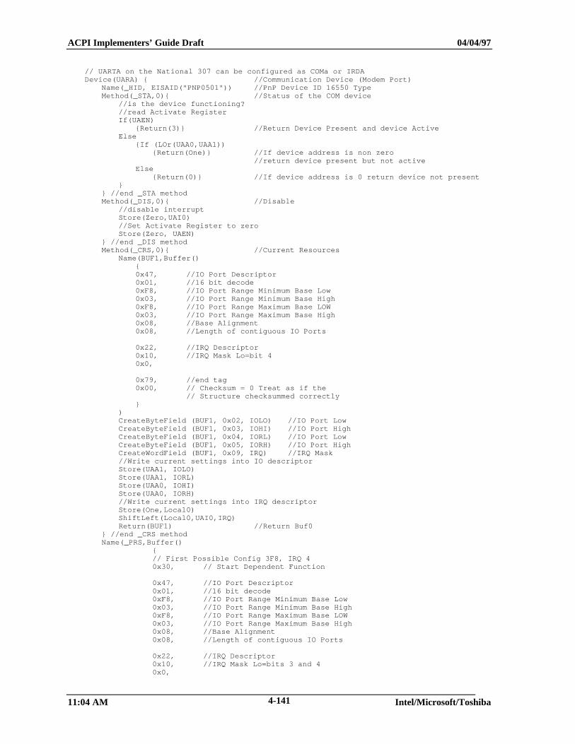
ACPI Implementers’ Guide Draft 04/04/97
11:04 AM Intel/Microsoft/Toshiba4-141
// UARTA on the National 307 can be configured as COMa or IRDADevice(UARA) { //Communication Device (Modem Port)
Name(_HID, EISAID("PNP0501")) //PnP Device ID 16550 TypeMethod(_STA,0){ //Status of the COM device
//is the device functioning?//read Activate RegisterIf(UAEN)
{Return(3)} //Return Device Present and device ActiveElse
{If (LOr(UAA0,UAA1)){Return(One)} //If device address is non zero
//return device present but not activeElse
{Return(0)} //If device address is 0 return device not present}
} //end _STA methodMethod(_DIS,0){ //Disable
//disable interruptStore(Zero,UAI0)//Set Activate Register to zeroStore(Zero, UAEN)
} //end _DIS methodMethod(_CRS,0){ //Current Resources
Name(BUF1,Buffer(){0x47, //IO Port Descriptor0x01, //16 bit decode0xF8, //IO Port Range Minimum Base Low0x03, //IO Port Range Minimum Base High0xF8, //IO Port Range Maximum Base LOW0x03, //IO Port Range Maximum Base High0x08, //Base Alignment0x08, //Length of contiguous IO Ports
0x22, //IRQ Descriptor0x10, //IRQ Mask Lo=bit 40x0,
0x79, //end tag0x00, // Checksum = 0 Treat as if the
// Structure checksummed correctly}
)CreateByteField (BUF1, 0x02, IOLO) //IO Port LowCreateByteField (BUF1, 0x03, IOHI) //IO Port HighCreateByteField (BUF1, 0x04, IORL) //IO Port LowCreateByteField (BUF1, 0x05, IORH) //IO Port HighCreateWordField (BUF1, 0x09, IRQ) //IRQ Mask//Write current settings into IO descriptorStore(UAA1, IOLO)Store(UAA1, IORL)Store(UAA0, IOHI)Store(UAA0, IORH)//Write current settings into IRQ descriptorStore(One,Local0)ShiftLeft(Local0,UAI0,IRQ)Return(BUF1) //Return Buf0
} //end _CRS methodName(_PRS,Buffer()
{// First Possible Config 3F8, IRQ 40x30, // Start Dependent Function
0x47, //IO Port Descriptor0x01, //16 bit decode0xF8, //IO Port Range Minimum Base Low0x03, //IO Port Range Minimum Base High0xF8, //IO Port Range Maximum Base LOW0x03, //IO Port Range Maximum Base High0x08, //Base Alignment0x08, //Length of contiguous IO Ports
0x22, //IRQ Descriptor0x10, //IRQ Mask Lo=bits 3 and 40x0,
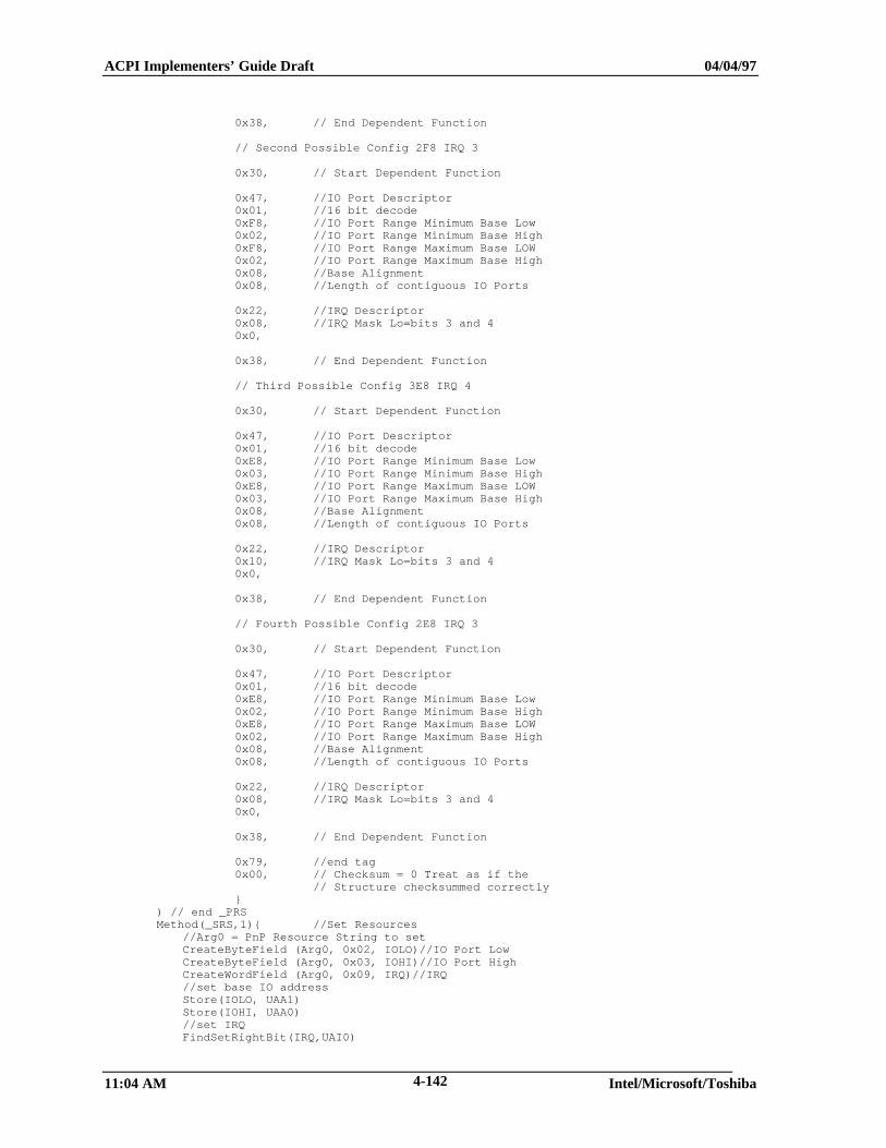
ACPI Implementers’ Guide Draft 04/04/97
11:04 AM Intel/Microsoft/Toshiba4-142
0x38, // End Dependent Function
// Second Possible Config 2F8 IRQ 3
0x30, // Start Dependent Function
0x47, //IO Port Descriptor0x01, //16 bit decode0xF8, //IO Port Range Minimum Base Low0x02, //IO Port Range Minimum Base High0xF8, //IO Port Range Maximum Base LOW0x02, //IO Port Range Maximum Base High0x08, //Base Alignment0x08, //Length of contiguous IO Ports
0x22, //IRQ Descriptor0x08, //IRQ Mask Lo=bits 3 and 40x0,
0x38, // End Dependent Function
// Third Possible Config 3E8 IRQ 4
0x30, // Start Dependent Function
0x47, //IO Port Descriptor0x01, //16 bit decode0xE8, //IO Port Range Minimum Base Low0x03, //IO Port Range Minimum Base High0xE8, //IO Port Range Maximum Base LOW0x03, //IO Port Range Maximum Base High0x08, //Base Alignment0x08, //Length of contiguous IO Ports
0x22, //IRQ Descriptor0x10, //IRQ Mask Lo=bits 3 and 40x0,
0x38, // End Dependent Function
// Fourth Possible Config 2E8 IRQ 3
0x30, // Start Dependent Function
0x47, //IO Port Descriptor0x01, //16 bit decode0xE8, //IO Port Range Minimum Base Low0x02, //IO Port Range Minimum Base High0xE8, //IO Port Range Maximum Base LOW0x02, //IO Port Range Maximum Base High0x08, //Base Alignment0x08, //Length of contiguous IO Ports
0x22, //IRQ Descriptor0x08, //IRQ Mask Lo=bits 3 and 40x0,
0x38, // End Dependent Function
0x79, //end tag0x00, // Checksum = 0 Treat as if the
// Structure checksummed correctly}
) // end _PRSMethod(_SRS,1){ //Set Resources
//Arg0 = PnP Resource String to setCreateByteField (Arg0, 0x02, IOLO)//IO Port LowCreateByteField (Arg0, 0x03, IOHI)//IO Port HighCreateWordField (Arg0, 0x09, IRQ)//IRQ//set base IO addressStore(IOLO, UAA1)Store(IOHI, UAA0)//set IRQFindSetRightBit(IRQ,UAI0)
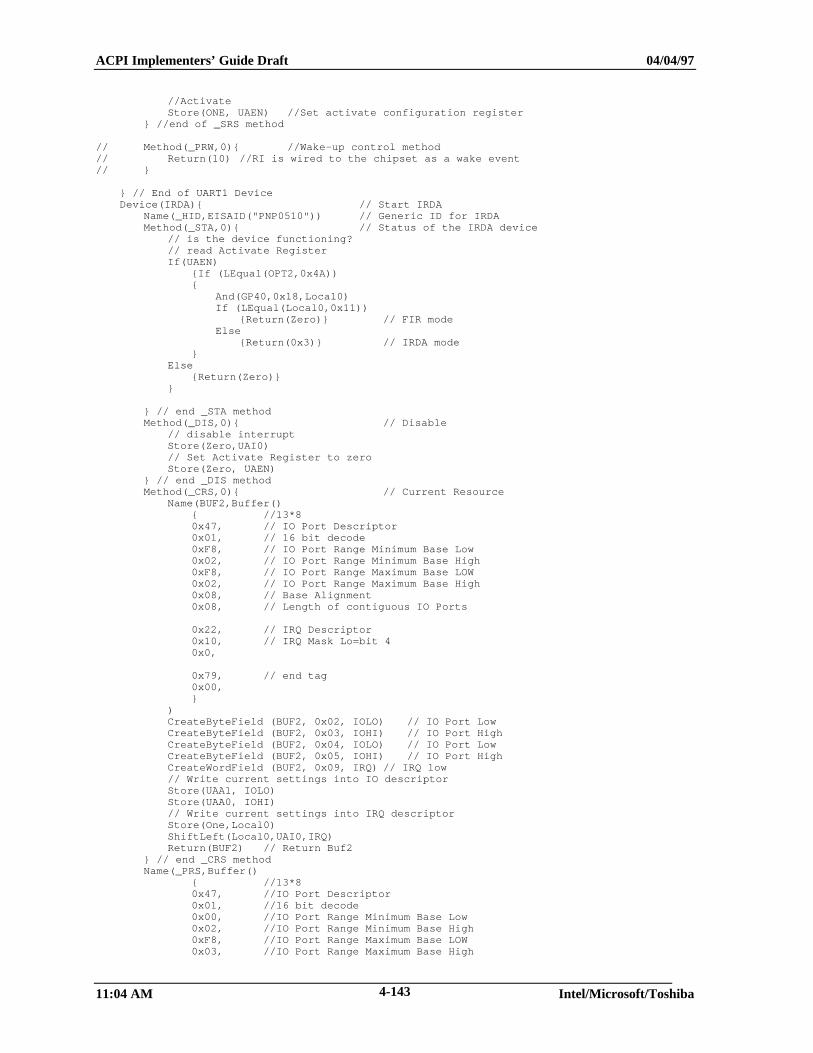
ACPI Implementers’ Guide Draft 04/04/97
11:04 AM Intel/Microsoft/Toshiba4-143
//ActivateStore(ONE, UAEN) //Set activate configuration register
} //end of _SRS method
// Method(_PRW,0){ //Wake-up control method// Return(10) //RI is wired to the chipset as a wake event// }
} // End of UART1 DeviceDevice(IRDA){ // Start IRDA
Name(_HID,EISAID("PNP0510")) // Generic ID for IRDAMethod(_STA,0){ // Status of the IRDA device
// is the device functioning?// read Activate RegisterIf(UAEN)
{If (LEqual(OPT2,0x4A)){
And(GP40,0x18,Local0)If (LEqual(Local0,0x11))
{Return(Zero)} // FIR modeElse
{Return(0x3)} // IRDA mode}
Else{Return(Zero)}
}
} // end _STA methodMethod(_DIS,0){ // Disable
// disable interruptStore(Zero,UAI0)// Set Activate Register to zeroStore(Zero, UAEN)
} // end _DIS methodMethod(_CRS,0){ // Current Resource
Name(BUF2,Buffer(){ //13*80x47, // IO Port Descriptor0x01, // 16 bit decode0xF8, // IO Port Range Minimum Base Low0x02, // IO Port Range Minimum Base High0xF8, // IO Port Range Maximum Base LOW0x02, // IO Port Range Maximum Base High0x08, // Base Alignment0x08, // Length of contiguous IO Ports
0x22, // IRQ Descriptor0x10, // IRQ Mask Lo=bit 40x0,
0x79, // end tag0x00,}
)CreateByteField (BUF2, 0x02, IOLO) // IO Port LowCreateByteField (BUF2, 0x03, IOHI) // IO Port HighCreateByteField (BUF2, 0x04, IOLO) // IO Port LowCreateByteField (BUF2, 0x05, IOHI) // IO Port HighCreateWordField (BUF2, 0x09, IRQ) // IRQ low// Write current settings into IO descriptorStore(UAA1, IOLO)Store(UAA0, IOHI)// Write current settings into IRQ descriptorStore(One,Local0)ShiftLeft(Local0,UAI0,IRQ)Return(BUF2) // Return Buf2
} // end _CRS methodName(_PRS,Buffer()
{ //13*80x47, //IO Port Descriptor0x01, //16 bit decode0x00, //IO Port Range Minimum Base Low0x02, //IO Port Range Minimum Base High0xF8, //IO Port Range Maximum Base LOW0x03, //IO Port Range Maximum Base High
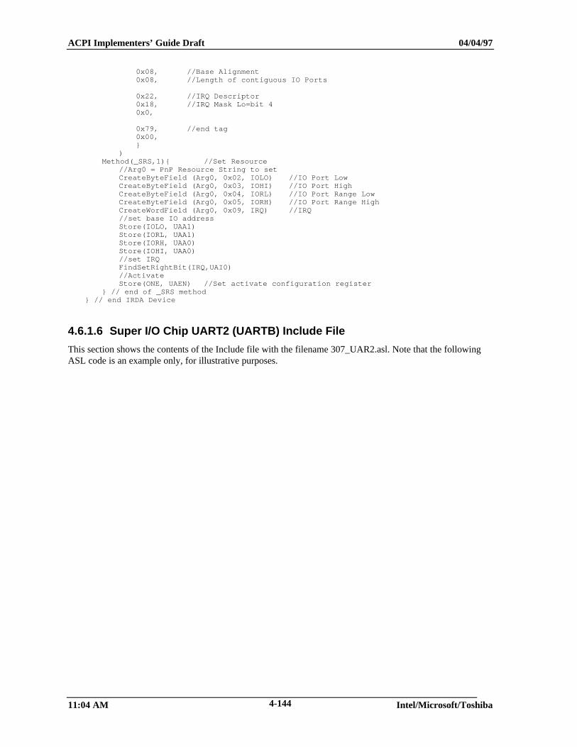
ACPI Implementers’ Guide Draft 04/04/97
11:04 AM Intel/Microsoft/Toshiba4-144
0x08, //Base Alignment0x08, //Length of contiguous IO Ports
0x22, //IRQ Descriptor0x18, //IRQ Mask Lo=bit 40x0,
0x79, //end tag0x00,}
)Method(_SRS,1){ //Set Resource
//Arg0 = PnP Resource String to setCreateByteField (Arg0, 0x02, IOLO) //IO Port LowCreateByteField (Arg0, 0x03, IOHI) //IO Port HighCreateByteField (Arg0, 0x04, IORL) //IO Port Range LowCreateByteField (Arg0, 0x05, IORH) //IO Port Range HighCreateWordField (Arg0, 0x09, IRQ) //IRQ//set base IO addressStore(IOLO, UAA1)Store(IORL, UAA1)Store(IORH, UAA0)Store(IOHI, UAA0)//set IRQFindSetRightBit(IRQ,UAI0)//ActivateStore(ONE, UAEN) //Set activate configuration register
} // end of _SRS method} // end IRDA Device
4.6.1.6 Super I/O Chip UART2 (UARTB) Include File
This section shows the contents of the Include file with the filename 307_UAR2.asl. Note that the followingASL code is an example only, for illustrative purposes.
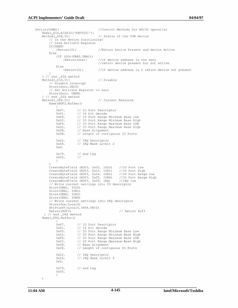
ACPI Implementers’ Guide Draft 04/04/97
11:04 AM Intel/Microsoft/Toshiba4-145
Device(COMB){ //Control Methods for RS232 operationName(_HID,EISAID("PNP0501"))Method(_STA,0){ // Status of the COM device
// is the device functioning?// read Activate RegisterIf(UBEN)
{Return(3)} //Return Device Present and device ActiveElse
{If (LOr(UBA0,UBA1)){Return(One)} //If device address is non zero
//return device present but not activeElse
{Return(0)} //If device address is 0 return device not present}
} // end _STA methodMethod(_DIS,0){ // Disable
// disable interruptStore(Zero,UBI0)// Set Activate Register to zeroStore(Zero, UBEN)
} // end _DIS methodMethod(_CRS,0){ // Current Resource
Name(BUF3,Buffer(){0x47, // IO Port Descriptor0x01, // 16 bit decode0xF8, // IO Port Range Minimum Base Low0x02, // IO Port Range Minimum Base High0xF8, // IO Port Range Maximum Base LOW0x02, // IO Port Range Maximum Base High0x08, // Base Alignment0x08, // Length of contiguous IO Ports
0x22, // IRQ Descriptor0x04, // IRQ Mask Lo=bit 20x0,
0x79, // end tag0x00, //}
)CreateByteField (BUF3, 0x02, IOLO) //IO Port LowCreateByteField (BUF3, 0x03, IOHI) //IO Port HighCreateByteField (BUF3, 0x04, IORL) //IO Port Range LowCreateByteField (BUF3, 0x05, IORH) //IO Port Range HighCreateWordField (BUF3, 0x09, IRQ) //IRQ low// Write current settings into IO descriptorStore(UBA1, IOLO)Store(UBA1, IORL)Store(UBA0, IOHI)Store(UBA0, IORH)// Write current settings into IRQ descriptorStore(One,Local0)ShiftLeft(Local0,INTR,UBI0)Return(BUF3) // Return Buf3
} // end _CRS methodName(_PRS,Buffer()
{0x47, // IO Port Descriptor0x01, // 16 bit decode0x00, // IO Port Range Minimum Base Low0x02, // IO Port Range Minimum Base High0xF8, // IO Port Range Maximum Base LOW0x03, // IO Port Range Maximum Base High0x08, // Base Alignment0x08, // Length of contiguous IO Ports
0x22, // IRQ Descriptor0x18, // IRQ Mask Lo=bit 40x0,
0x79, // end tag0x00,}
)
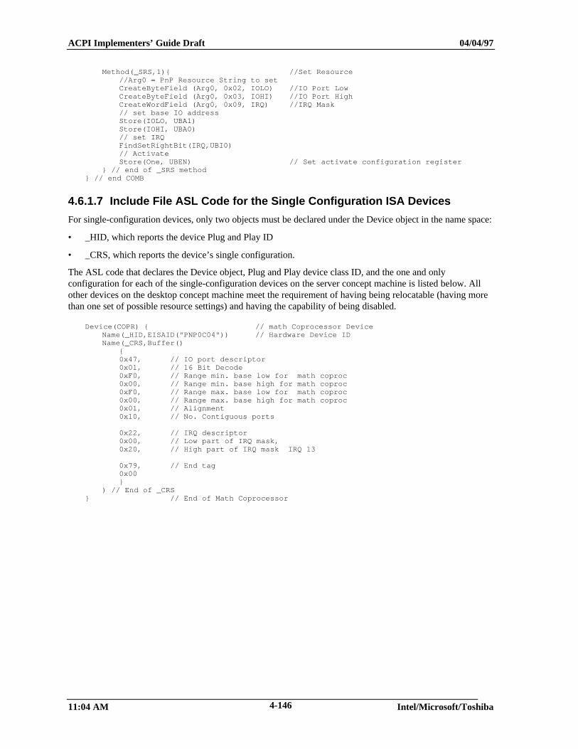
ACPI Implementers’ Guide Draft 04/04/97
11:04 AM Intel/Microsoft/Toshiba4-146
Method(_SRS,1){ //Set Resource//Arg0 = PnP Resource String to setCreateByteField (Arg0, 0x02, IOLO) //IO Port LowCreateByteField (Arg0, 0x03, IOHI) //IO Port HighCreateWordField (Arg0, 0x09, IRQ) //IRQ Mask// set base IO addressStore(IOLO, UBA1)Store(IOHI, UBA0)// set IRQFindSetRightBit(IRQ,UBI0)// ActivateStore(One, UBEN) // Set activate configuration register
} // end of _SRS method} // end COMB
4.6.1.7 Include File ASL Code for the Single Configuration ISA Devices
For single-configuration devices, only two objects must be declared under the Device object in the name space:
• _HID, which reports the device Plug and Play ID
• _CRS, which reports the device’s single configuration.
The ASL code that declares the Device object, Plug and Play device class ID, and the one and onlyconfiguration for each of the single-configuration devices on the server concept machine is listed below. Allother devices on the desktop concept machine meet the requirement of having being relocatable (having morethan one set of possible resource settings) and having the capability of being disabled.
Device(COPR) { // math Coprocessor DeviceName(_HID,EISAID("PNP0C04")) // Hardware Device IDName(_CRS,Buffer()
{0x47, // IO port descriptor0x01, // 16 Bit Decode0xF0, // Range min. base low for math coproc0x00, // Range min. base high for math coproc0xF0, // Range max. base low for math coproc0x00, // Range max. base high for math coproc0x01, // Alignment0x10, // No. Contiguous ports
0x22, // IRQ descriptor0x00, // Low part of IRQ mask,0x20, // High part of IRQ mask IRQ 13
0x79, // End tag0x00}
) // End of _CRS} // End of Math Coprocessor
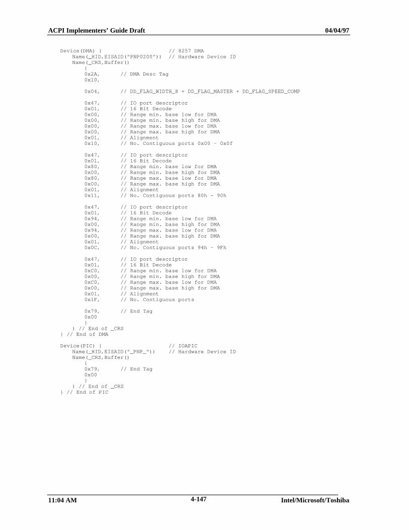
ACPI Implementers’ Guide Draft 04/04/97
11:04 AM Intel/Microsoft/Toshiba4-147
Device(DMA) { // 8257 DMAName(_HID,EISAID("PNP0200")) // Hardware Device IDName(_CRS,Buffer()
{0x2A, // DMA Desc Tag0x10,
0x04, // DD_FLAG_WIDTH_8 + DD_FLAG_MASTER + DD_FLAG_SPEED_COMP
0x47, // IO port descriptor0x01, // 16 Bit Decode0x00, // Range min. base low for DMA0x00, // Range min. base high for DMA0x00, // Range max. base low for DMA0x00, // Range max. base high for DMA0x01, // Alignment0x10, // No. Contiguous ports 0x00 - 0x0f
0x47, // IO port descriptor0x01, // 16 Bit Decode0x80, // Range min. base low for DMA0x00, // Range min. base high for DMA0x80, // Range max. base low for DMA0x00, // Range max. base high for DMA0x01, // Alignment0x11, // No. Contiguous ports 80h - 90h
0x47, // IO port descriptor0x01, // 16 Bit Decode0x94, // Range min. base low for DMA0x00, // Range min. base high for DMA0x94, // Range max. base low for DMA0x00, // Range max. base high for DMA0x01, // Alignment0x0C, // No. Contiguous ports 94h - 9Fh
0x47, // IO port descriptor0x01, // 16 Bit Decode0xC0, // Range min. base low for DMA0x00, // Range min. base high for DMA0xC0, // Range max. base low for DMA0x00, // Range max. base high for DMA0x01, // Alignment0x1F, // No. Contiguous ports
0x79, // End Tag0x00}
) // End of _CRS} // End of DMA
Device(PIC) { // IOAPICName(_HID,EISAID("_PNP_")) // Hardware Device IDName(_CRS,Buffer()
{0x79, // End Tag0x00}
) // End of _CRS} // End of PIC
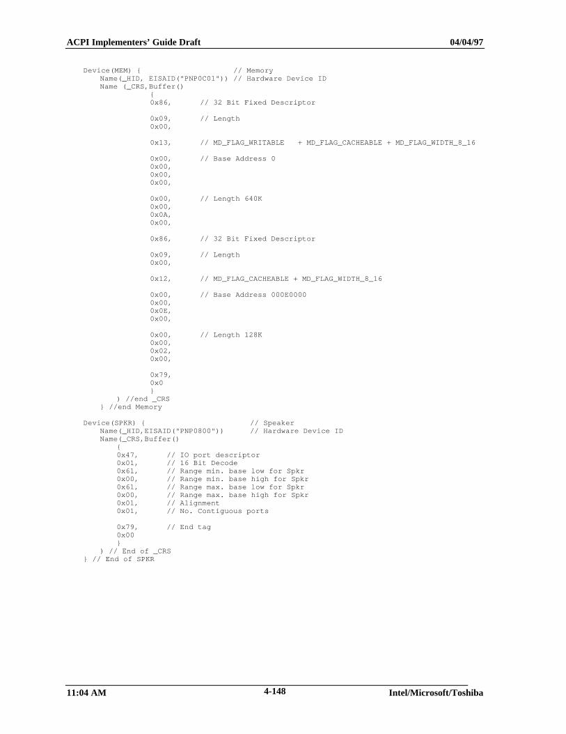
ACPI Implementers’ Guide Draft 04/04/97
11:04 AM Intel/Microsoft/Toshiba4-148
Device(MEM) { // MemoryName(_HID, EISAID("PNP0C01")) // Hardware Device IDName (_CRS,Buffer()
{0x86, // 32 Bit Fixed Descriptor
0x09, // Length0x00,
0x13, // MD_FLAG_WRITABLE + MD_FLAG_CACHEABLE + MD_FLAG_WIDTH_8_16
0x00, // Base Address 00x00,0x00,0x00,
0x00, // Length 640K0x00,0x0A,0x00,
0x86, // 32 Bit Fixed Descriptor
0x09, // Length0x00,
0x12, // MD_FLAG_CACHEABLE + MD_FLAG_WIDTH_8_16
0x00, // Base Address 000E00000x00,0x0E,0x00,
0x00, // Length 128K0x00,0x02,0x00,
0x79,0x0}
) //end _CRS} //end Memory
Device(SPKR) { // SpeakerName(_HID,EISAID("PNP0800")) // Hardware Device IDName(_CRS,Buffer()
{0x47, // IO port descriptor0x01, // 16 Bit Decode0x61, // Range min. base low for Spkr0x00, // Range min. base high for Spkr0x61, // Range max. base low for Spkr0x00, // Range max. base high for Spkr0x01, // Alignment0x01, // No. Contiguous ports
0x79, // End tag0x00}
) // End of _CRS} // End of SPKR
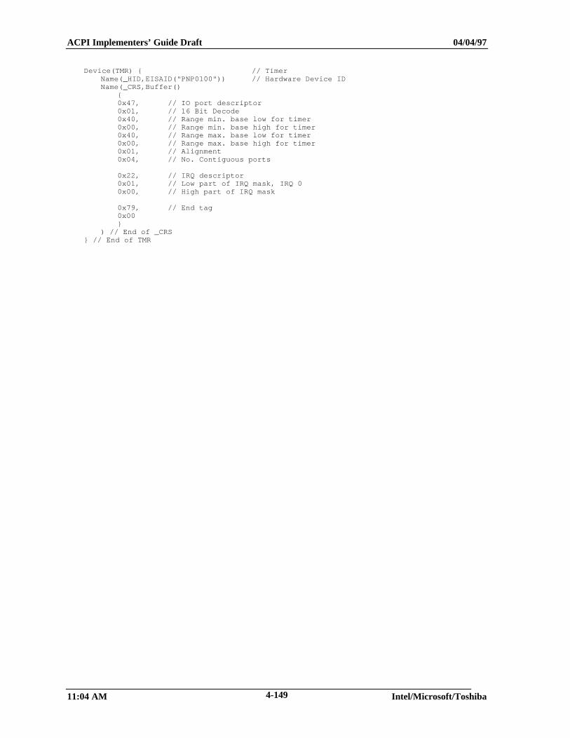
ACPI Implementers’ Guide Draft 04/04/97
11:04 AM Intel/Microsoft/Toshiba4-149
Device(TMR) { // TimerName(_HID,EISAID("PNP0100")) // Hardware Device IDName(_CRS,Buffer()
{0x47, // IO port descriptor0x01, // 16 Bit Decode0x40, // Range min. base low for timer0x00, // Range min. base high for timer0x40, // Range max. base low for timer0x00, // Range max. base high for timer0x01, // Alignment0x04, // No. Contiguous ports
0x22, // IRQ descriptor0x01, // Low part of IRQ mask, IRQ 00x00, // High part of IRQ mask
0x79, // End tag0x00}
) // End of _CRS} // End of TMR

ACPI Implementers’ Guide Draft 04/04/97
11:04 AM Intel/Microsoft/Toshiba4-150
.
ACPI Implementers’ Guide Draft 04/04/97
11:04 AM Intel/Microsoft/Toshiba5-151
5. ACPI BIOS Case Study
This section uses the ACPI-compatible Trajan 430TX motherboard as a case study and shows how to build anACPI BIOS for an actual ACPI-compatible motherboard product. The Trajan 430TX is available for customersfor evaluation along with source code for the following functionality:
• Chipset start up
• Memory sizing
• Chipset register initialization
• Cache initialization
• Legacy power management functions
• Legacy docking functions
• SMBus functions
Besides describing the functionality listed above (with ACPI name space and ASL code examples), this sectionof the Guide focuses on the role of an ACPI BIOS during system state transitions:
• During the cold boot sequence.
• Waking up from S1
• Waking up from S2
• Waking up from S3
• Waking up from S4
• Switching between ACPI and Legacy modes
This section also focuses on how ACPI can be used on a Trajan motherboard to accomplish
• Power management
• Device Plug and Play
5.1 Trajan Architecture
Features of the Trajan architecture are:
• Intel 430 TX chipset with a P55C processor.
• EIO bus supporting the following components:
• BIOS ROM
• ISA slots
• National 87338 Super I/O chip
• ESS 1888 Sound device
• SMBus supporting an embedded controller interface to a smart battery
• Thermal management support using a PIIX-4 interface to a National LM-75 Temperature Controller
• A PCI root bus with the following components attached:
• TI 1130 CardBus Controller
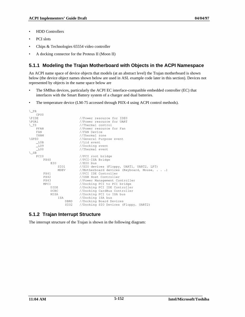
ACPI Implementers’ Guide Draft 04/04/97
11:04 AM Intel/Microsoft/Toshiba5-152
• HDD Controllers
• PCI slots
• Chips & Technologies 65554 video controller
• A docking connector for the Proteus II (Moon II)
5.1.1 Modeling the Trajan Motherboard with Objects in the ACPI Namespace
An ACPI name space of device objects that models (at an abstract level) the Trajan motherboard is shownbelow (the device object names shown below are used in ASL example code later in this section). Devices notrepresented by objects in the name space below are
• The SMBus devices, particularly the ACPI EC interface-compatible embedded controller (EC) thatinterfaces with the Smart Battery system of a charger and dual batteries.
• The temperature device (LM-75 accessed through PIIX-4 using ACPI control methods).
\_PRCPU0
\PIDE //Power resource for IDE0\PUA1 //Power resource for UART\_TZ //Thermal control
PFAN //Power resource for FanFAN //FAN DeviceTHRM //Thermal zone
\GPE0 //General Purpose event_L0B //Lid event_L09 //Docking event_L00 //Thermal event
\_SBPCI0 //PCI root bridge
PX40 //PCI-ISA BridgeEIO //EIO bus
SIO1 //SIO devices (Floppy, UART1, UART2, LPT)MDEV //Motherboard devices (Keyboard, Mouse, . . .)
PX41 //PCI IDE ControllerPX42 //USB Host ControllerPX43 //Power Management ControllerMPCI //Docking PCI to PCI bridge
DIDE //Docking PCI IDE ControllerDCBC //Docking CardBus ControllerMISA //Docking PCI to ISA bus
ISA //Docking ISA busDBRD //Docking Board DevicesSIO2 //Docking SIO Devices (Floppy, UART2)
5.1.2 Trajan Interrupt Structure
The interrupt structure of the Trajan is shown in the following diagram:
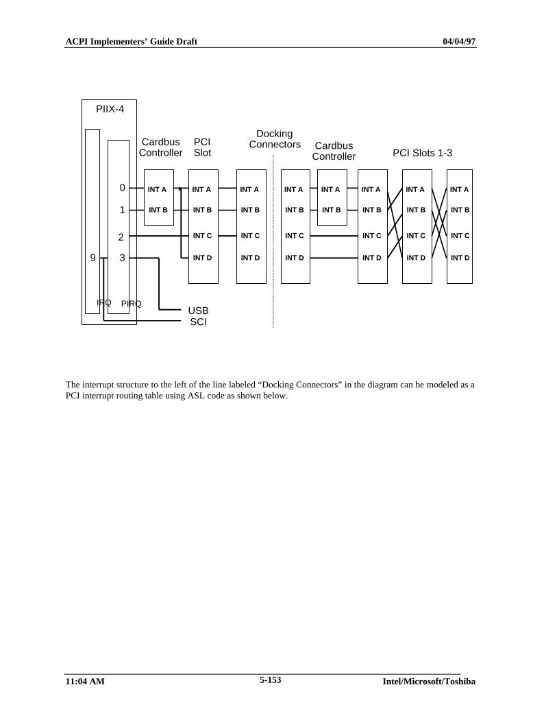
ACPI Implementers’ Guide Draft 04/04/97
11:04 AM Intel/Microsoft/Toshiba5-153
INT A
INT B
INT A
INT B
INT C
INT D
INT A
INT B
INT C
INT D
INT A
INT B
INT C
INT D
INT A
INT B
INT C
INT D
INT A
INT B
INT C
INT D
s
DockingConnectorsPCI
SlotCardbus
Controller
INT A
INT B
INT C
INT D
INT A
INT B
PIIX-4
PIRQ
2
1
0
IRQ
9
USB
3
CardbusController PCI Slots 1-3
SCI
The interrupt structure to the left of the line labeled “Docking Connectors” in the diagram can be modeled as aPCI interrupt routing table using ASL code as shown below.
ACPI Implementers’ Guide Draft 04/04/97
11:04 AM Intel/Microsoft/Toshiba5-154
// PCI interrupt linkDevice(LNKA) {
Name(_HID, EISAID("PNP0C0F"))Name(_UID, 1)Name(_PRS, Buffer(){
// IRQ descriptor, level, low, IRQ3-7,9-12,14,150x22, 0xF8, 0xDE, 0x18,// End tag0x79, 0})
Method(_DIS) {// Disable PIRQ routingAnd(PIRA, 0x7F, PIRA)
}Method(_CRS) {
Name(BUFA, Buffer(){// IRQ descriptor, level, low, IRQ3-7,9-12,14,150x22, 0x00, 0x00, 0x18,// End tag0x79, 0})
CreateByteField(BUFA, 0x01, IRA1) // IRQ mask 1CreateByteField(BUFA, 0x02, IRA2) // IRQ mask 2And(PIRA, 0x8F, Local0)If(LGreater(Local0, 0x80)) { // Routing enable
And(Local0, 0x0F) // Mask off enable bitIf(LGreater(Local0, 0x07)) {
Subtract(Local0, 8)Store(Local0, IRA2)}
Else {Store(Local0, IRA1)}
}Return(BUFA)
} // Method(_CRS)Method(_SRS, 1) {
// ARG0 = PnP resource string to set// (IRQ ordering assumed to be same as _PRS/_CRS)CreateByteField(ARG0, 0x01, IRA1) // IRQ mask 1CreateByteField(ARG0, 0x02, IRA2) // IRQ mask 2If(LGreater(IRA2, Zero)) {
Add(IRA2, 8)}Else {
Store(IRA1, IRA2)}// Enable and set PIRQ routingAnd(PIRA, 0xF0, Local0)Or(Local0, 0x80, Local0)Or(IRA2, Local0, PIRA)
}} // Device(LNKA)
//Device(LNKB) {
Name(_HID, EISAID("PNP0C0F"))Name(_UID, 2)Name(_PRS, Buffer(){
// IRQ descriptor, level, low, IRQ3-7,9-12,14,150x22, 0xF8, 0xDE, 0x18,// End tag0x79, 0})
Method(_DIS) {// Disable PIRQ routingAnd(PIRB, 0x7F, PIRB)
}Method(_CRS) {
Name(BUFB, Buffer(){// IRQ descriptor, level, low, IRQ3-7,9-12,14,150x22, 0x00, 0x00, 0x18,// End tag0x79, 0})
CreateByteField(BUFB, 0x01, IRB1) // IRQ mask 1CreateByteField(BUFB, 0x02, IRB2) // IRQ mask 2And(PIRB, 0x8F, Local0)If(LGreater(Local0, 0x80)) { // Routing enable
And(Local0, 0x0F) // Mask off enable bitIf(LGreater(Local0, 0x07)) {
Subtract(Local0, 8)Store(Local0, IRB2)}
Else {
ACPI Implementers’ Guide Draft 04/04/97
11:04 AM Intel/Microsoft/Toshiba5-155
Store(Local0, IRB1)}}Return(BUFB)
} // Method(_CRS)Method(_SRS, 1) {
// ARG0 = PnP resource string to set// (IRQ ordering assumed to be same as _PRS/_CRS)CreateByteField(ARG0, 0x01, IRB1) // IRQ mask 1CreateByteField(ARG0, 0x02, IRB2) // IRQ mask 2If(LGreater(IRB2, Zero)) {
Add(IRB2, 8)}Else {
Store(IRB1, IRB2)}// Enable and set PIRQ routingAnd(PIRB, 0xF0, Local0)Or(Local0, 0x80, Local0)Or(IRB2, Local0, PIRB)}
} // Device(LNKB)//
Device(LNKC) {Name(_HID, EISAID("PNP0C0F"))Name(_UID, 3)Name(_PRS, Buffer(){
// IRQ descriptor, level, low, IRQ3-7,9-12,14,150x22, 0xF8, 0xDE, 0x18,// End tag0x79, 0})
Method(_DIS) {// Disable PIRQ routingAnd(PIRC, 0x7F, PIRC)
}Method(_CRS) {
Name(BUFC, Buffer(){// IRQ descriptor, level, low, IRQ3-7,9-12,14,150x22, 0x00, 0x00, 0x18,// End tag0x79, 0})
CreateByteField(BUFC, 0x01, IRC1) // IRQ mask 1CreateByteField(BUFC, 0x02, IRC2) // IRQ mask 2And(PIRC, 0x8F, Local0)If(LGreater(Local0, 0x80)) { // Routing enable
And(Local0, 0x0F) // Mask off enable bitIf(LGreater(Local0, 0x07)) {
Subtract(Local0, 8)Store(Local0, IRC2)}
Else {Store(Local0, IRC1)}
}Return(BUFC)
} // Method(_CRS)Method(_SRS, 1) {
// ARG0 = PnP resource string to set// (IRQ ordering assumed to be same as _PRS/_CRS)CreateByteField(ARG0, 0x01, IRC1) // IRQ mask 1CreateByteField(ARG0, 0x02, IRC2) // IRQ mask 2If(LGreater(IRC2, Zero)) {
Add(IRC2, 8)}Else {
Store(IRC1, IRC2)}// Enable and set PIRQ routingAnd(PIRC, 0xF0, Local0)Or(Local0, 0x80, Local0)Or(IRC2, Local0, PIRC)
}} // Device(LNKC)Device(LNKD) {
Name(_HID, EISAID("PNP0C0F"))Name(_UID, 4)Name(_PRS, Buffer(){
// IRQ descriptor, level, low, IRQ3-7,9-12,14,150x22, 0xF8, 0xDE, 0x18,// End tag0x79, 0})
Method(_DIS) {
ACPI Implementers’ Guide Draft 04/04/97
11:04 AM Intel/Microsoft/Toshiba5-156
// Disable PIRQ routingAnd(PIRD, 0x7F, PIRD)
}Method(_CRS) {
Name(BUFD, Buffer(){// IRQ descriptor, level, low, IRQ3-7,9-12,14,150x22, 0x00, 0x00, 0x18,// End tag0x79, 0})
CreateByteField(BUFD, 0x01, IRD1) // IRQ mask 1CreateByteField(BUFD, 0x02, IRD2) // IRQ mask 2And(PIRD, 0x8F, Local0)If(LGreater(Local0, 0x80)) { // Routing enable
And(Local0, 0x0F) // Mask off enable bitIf(LGreater(Local0, 0x07)) {
Subtract(Local0, 8)Store(Local0, IRD2)}
Else {Store(Local0, IRD1)}
}Return(BUFD)
} // Method(_CRS)Method(_SRS, 1) {
// ARG0 = PnP resource string to set// (IRQ ordering assumed to be same as _PRS/_CRS)CreateByteField(ARG0, 0x01, IRD1) // IRQ mask 1CreateByteField(ARG0, 0x02, IRD2) // IRQ mask 2If(LGreater(IRD2, Zero)) {
Add(IRD2, 8)}Else {
Store(IRD1, IRD2)}// Enable and set PIRQ routingAnd(PIRD, 0xF0, Local0)Or(Local0, 0x80, Local0)Or(IRD2, Local0, PIRD)
}} // Device(LNKD)
.
.
.// PCI Bus/DeviceDevice(PCI0) {
Name(_HID, EISAID("PNP0A03")) // PCI root bus IDName(_ADR, 0x00000000) // word dev/func = 0/0Name(_CRS, 0) // bus 0 (for root bus only)Name(_PRT, Package(){
Package(){0x0001FFFF, 0, LNKA, 0},Package(){0x0001FFFF, 1, LNKB, 0},Package(){0x0001FFFF, 2, LNKC, 0},Package(){0x0001FFFF, 3, LNKD, 0},Package(){0x0004FFFF, 0, LNKA, 0},Package(){0x0004FFFF, 1, LNKB, 0},Package(){0x0004FFFF, 2, LNKC, 0},Package(){0x0004FFFF, 3, LNKA, 0},Package(){0x000AFFFF, 0, LNKA, 0},Package(){0x000AFFFF, 1, LNKB, 0}})
.
.
.
5.2 Initializing the ACPI BIOS During POST and Cold Boot Sequence
Initializing the ACPI BIOS is one step in the cold boot sequence of the Trajan. The steps in the cold bootsequence are shown below; initializing the ACPI BIOS is the next to the last step:
1. Memory testing and configuration.
2. BIOS shadow.
3. Minimal test of motherboard devices.
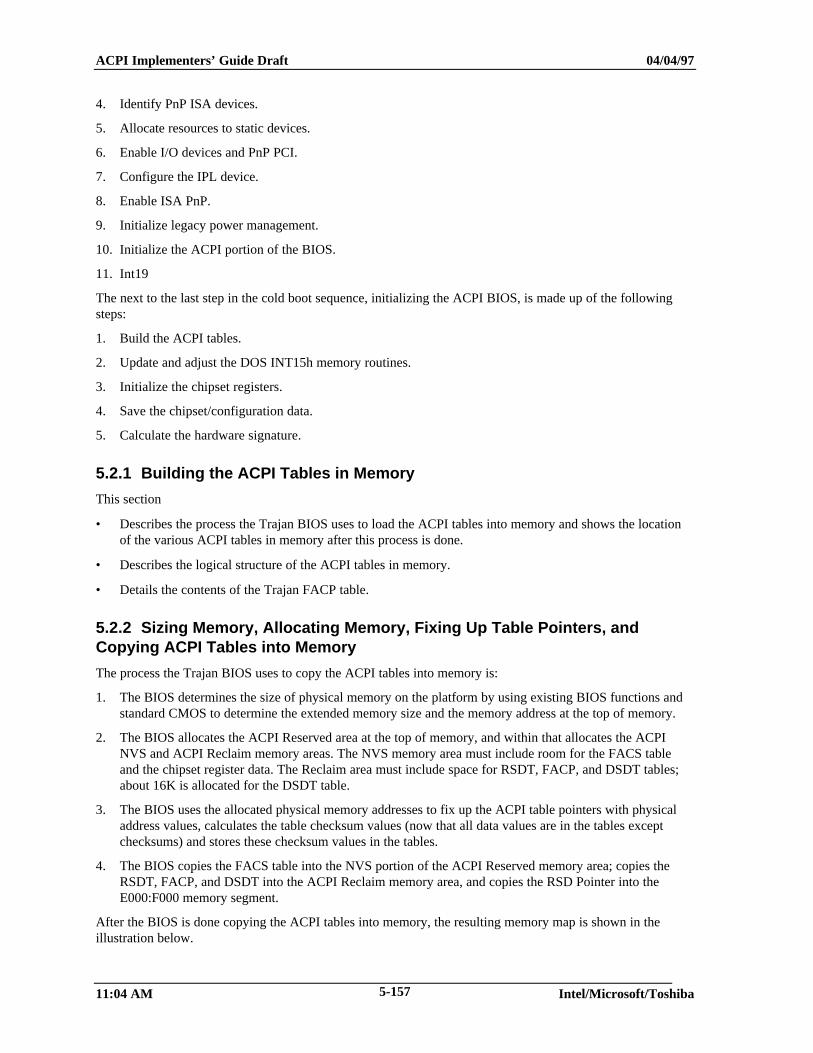
ACPI Implementers’ Guide Draft 04/04/97
11:04 AM Intel/Microsoft/Toshiba5-157
4. Identify PnP ISA devices.
5. Allocate resources to static devices.
6. Enable I/O devices and PnP PCI.
7. Configure the IPL device.
8. Enable ISA PnP.
9. Initialize legacy power management.
10. Initialize the ACPI portion of the BIOS.
11. Int19
The next to the last step in the cold boot sequence, initializing the ACPI BIOS, is made up of the followingsteps:
1. Build the ACPI tables.
2. Update and adjust the DOS INT15h memory routines.
3. Initialize the chipset registers.
4. Save the chipset/configuration data.
5. Calculate the hardware signature.
5.2.1 Building the ACPI Tables in Memory
This section
• Describes the process the Trajan BIOS uses to load the ACPI tables into memory and shows the locationof the various ACPI tables in memory after this process is done.
• Describes the logical structure of the ACPI tables in memory.
• Details the contents of the Trajan FACP table.
5.2.2 Sizing Memory, Allocating Memory, Fixing Up Table Pointers, andCopying ACPI Tables into Memory
The process the Trajan BIOS uses to copy the ACPI tables into memory is:
1. The BIOS determines the size of physical memory on the platform by using existing BIOS functions andstandard CMOS to determine the extended memory size and the memory address at the top of memory.
2. The BIOS allocates the ACPI Reserved area at the top of memory, and within that allocates the ACPINVS and ACPI Reclaim memory areas. The NVS memory area must include room for the FACS tableand the chipset register data. The Reclaim area must include space for RSDT, FACP, and DSDT tables;about 16K is allocated for the DSDT table.
3. The BIOS uses the allocated physical memory addresses to fix up the ACPI table pointers with physicaladdress values, calculates the table checksum values (now that all data values are in the tables exceptchecksums) and stores these checksum values in the tables.
4. The BIOS copies the FACS table into the NVS portion of the ACPI Reserved memory area; copies theRSDT, FACP, and DSDT into the ACPI Reclaim memory area, and copies the RSD Pointer into theE000:F000 memory segment.
After the BIOS is done copying the ACPI tables into memory, the resulting memory map is shown in theillustration below.
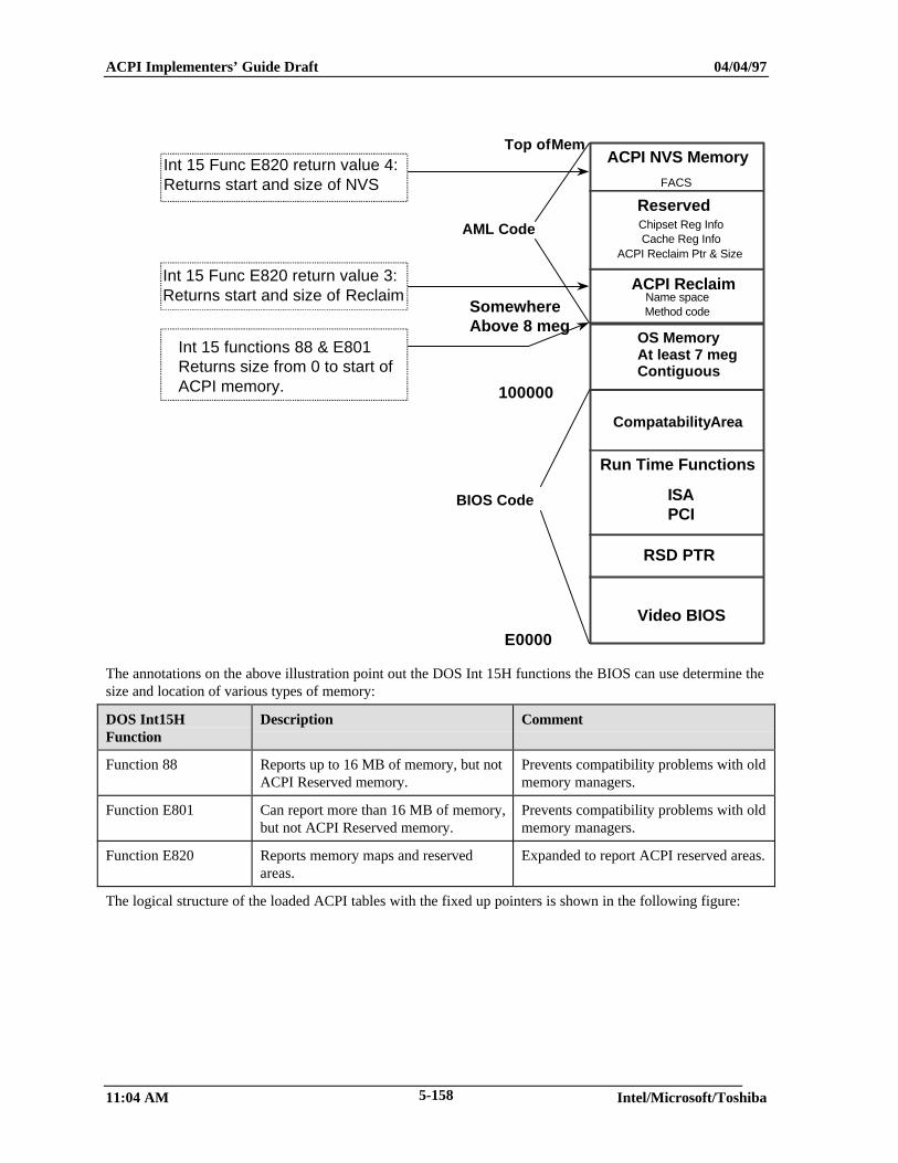
ACPI Implementers’ Guide Draft 04/04/97
11:04 AM Intel/Microsoft/Toshiba5-158
100000
Compatability Area
Video BIOS
Run Time Functions
ISAPCI
Top of MemACPI NVS Memory
Reserved
ACPI Reclaim
RSD PTR
FACS
Chipset Reg InfoCache Reg Info
ACPI Reclaim Ptr & Size
Name spaceMethod codeSomewhere
Above 8 megOS MemoryAt least 7 megContiguous
AML Code
BIOS Code
E0000
Int 15 functions 88 & E801Returns size from 0 to start ofACPI memory.
Int 15 Func E820 return value 4:Returns start and size of NVS
Int 15 Func E820 return value 3:Returns start and size of Reclaim
The annotations on the above illustration point out the DOS Int 15H functions the BIOS can use determine thesize and location of various types of memory:
DOS Int15HFunction
Description Comment
Function 88 Reports up to 16 MB of memory, but notACPI Reserved memory.
Prevents compatibility problems with oldmemory managers.
Function E801 Can report more than 16 MB of memory,but not ACPI Reserved memory.
Prevents compatibility problems with oldmemory managers.
Function E820 Reports memory maps and reservedareas.
Expanded to report ACPI reserved areas.
The logical structure of the loaded ACPI tables with the fixed up pointers is shown in the following figure:
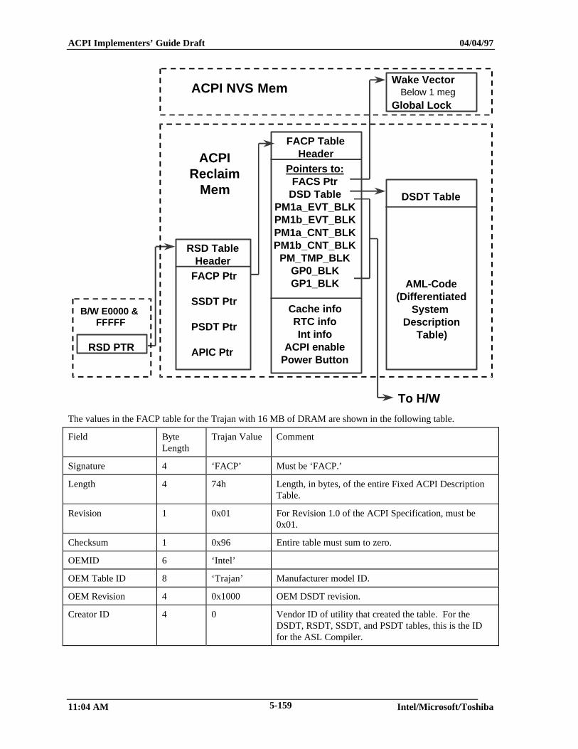
ACPI Implementers’ Guide Draft 04/04/97
11:04 AM Intel/Microsoft/Toshiba5-159
RSD PTR
B/W E0000 & FFFFF
ACPIReclaim
Mem
RSD TableHeader
FACP Ptr
SSDT Ptr
PSDT Ptr
APIC Ptr
FACP TableHeader
Pointers to:FACS Ptr
DSD TablePM1a_EVT_BLKPM1b_EVT_BLKPM1a_CNT_BLKPM1b_CNT_BLK
PM_TMP_BLKGP0_BLKGP1_BLK
Cache infoRTC infoInt info
ACPI enablePower Button
DSDT Table
AML-Code(Differentiated
SystemDescription
Table)
Wake VectorBelow 1 meg
Global Lock
ACPI NVS Mem
To H/W
The values in the FACP table for the Trajan with 16 MB of DRAM are shown in the following table.
Field ByteLength
Trajan Value Comment
Signature 4 ‘FACP’ Must be ‘FACP.’
Length 4 74h Length, in bytes, of the entire Fixed ACPI DescriptionTable.
Revision 1 0x01 For Revision 1.0 of the ACPI Specification, must be0x01.
Checksum 1 0x96 Entire table must sum to zero.
OEMID 6 ‘Intel’
OEM Table ID 8 ‘Trajan’ Manufacturer model ID.
OEM Revision 4 0x1000 OEM DSDT revision.
Creator ID 4 0 Vendor ID of utility that created the table. For theDSDT, RSDT, SSDT, and PSDT tables, this is the IDfor the ASL Compiler.
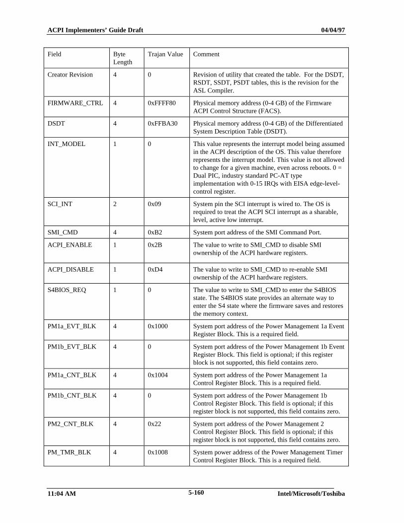
ACPI Implementers’ Guide Draft 04/04/97
11:04 AM Intel/Microsoft/Toshiba5-160
Field ByteLength
Trajan Value Comment
Creator Revision 4 0 Revision of utility that created the table. For the DSDT,RSDT, SSDT, PSDT tables, this is the revision for theASL Compiler.
FIRMWARE_CTRL 4 0xFFFF80 Physical memory address (0-4 GB) of the FirmwareACPI Control Structure (FACS).
DSDT 4 0xFFBA30 Physical memory address (0-4 GB) of the DifferentiatedSystem Description Table (DSDT).
INT_MODEL 1 0 This value represents the interrupt model being assumedin the ACPI description of the OS. This value thereforerepresents the interrupt model. This value is not allowedto change for a given machine, even across reboots. 0 =Dual PIC, industry standard PC-AT typeimplementation with 0-15 IRQs with EISA edge-level-control register.
SCI_INT 2 0x09 System pin the SCI interrupt is wired to. The OS isrequired to treat the ACPI SCI interrupt as a sharable,level, active low interrupt.
SMI_CMD 4 0xB2 System port address of the SMI Command Port.
ACPI_ENABLE 1 0x2B The value to write to SMI_CMD to disable SMIownership of the ACPI hardware registers.
ACPI_DISABLE 1 0xD4 The value to write to SMI_CMD to re-enable SMIownership of the ACPI hardware registers.
S4BIOS_REQ 1 0 The value to write to SMI_CMD to enter the S4BIOSstate. The S4BIOS state provides an alternate way toenter the S4 state where the firmware saves and restoresthe memory context.
PM1a_EVT_BLK 4 0x1000 System port address of the Power Management 1a EventRegister Block. This is a required field.
PM1b_EVT_BLK 4 0 System port address of the Power Management 1b EventRegister Block. This field is optional; if this registerblock is not supported, this field contains zero.
PM1a_CNT_BLK 4 0x1004 System port address of the Power Management 1aControl Register Block. This is a required field.
PM1b_CNT_BLK 4 0 System port address of the Power Management 1bControl Register Block. This field is optional; if thisregister block is not supported, this field contains zero.
PM2_CNT_BLK 4 0x22 System port address of the Power Management 2Control Register Block. This field is optional; if thisregister block is not supported, this field contains zero.
PM_TMR_BLK 4 0x1008 System power address of the Power Management TimerControl Register Block. This is a required field.
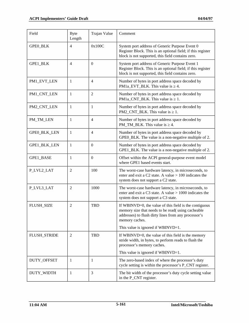
ACPI Implementers’ Guide Draft 04/04/97
11:04 AM Intel/Microsoft/Toshiba5-161
Field ByteLength
Trajan Value Comment
GPE0_BLK 4 0x100C System port address of Generic Purpose Event 0Register Block. This is an optional field; if this registerblock is not supported, this field contains zero.
GPE1_BLK 4 0 System port address of Generic Purpose Event 1Register Block. This is an optional field; if this registerblock is not supported, this field contains zero.
PM1_EVT_LEN 1 4 Number of bytes in port address space decoded byPM1a_EVT_BLK. This value is ≥ 4.
PM1_CNT_LEN 1 2 Number of bytes in port address space decoded byPM1a_CNT_BLK. This value is ≥ 1.
PM2_CNT_LEN 1 1 Number of bytes in port address space decoded byPM2_CNT_BLK. This value is ≥ 1.
PM_TM_LEN 1 4 Number of bytes in port address space decoded byPM_TM_BLK. This value is ≥ 4.
GPE0_BLK_LEN 1 4 Number of bytes in port address space decoded byGPE0_BLK. The value is a non-negative multiple of 2.
GPE1_BLK_LEN 1 0 Number of bytes in port address space decoded byGPE1_BLK. The value is a non-negative multiple of 2.
GPE1_BASE 1 0 Offset within the ACPI general-purpose event modelwhere GPE1 based events start.
P_LVL2_LAT 2 100 The worst-case hardware latency, in microseconds, toenter and exit a C2 state. A value > 100 indicates thesystem does not support a C2 state.
P_LVL3_LAT 2 1000 The worst-case hardware latency, in microseconds, toenter and exit a C3 state. A value > 1000 indicates thesystem does not support a C3 state.
FLUSH_SIZE 2 TBD If WBINVD=0, the value of this field is the contiguousmemory size that needs to be read( using cacheableaddresses) to flush dirty lines from any processor’smemory caches.
This value is ignored if WBINVD=1.
FLUSH_STRIDE 2 TBD If WBINVD=0, the value of this field is the memorystride width, in bytes, to perform reads to flush theprocessor’s memory caches.
This value is ignored if WBINVD=1.
DUTY_OFFSET 1 1 The zero-based index of where the processor’s dutycycle setting is within the processor’s P_CNT register.
DUTY_WIDTH 1 3 The bit width of the processor’s duty cycle setting valuein the P_CNT register.
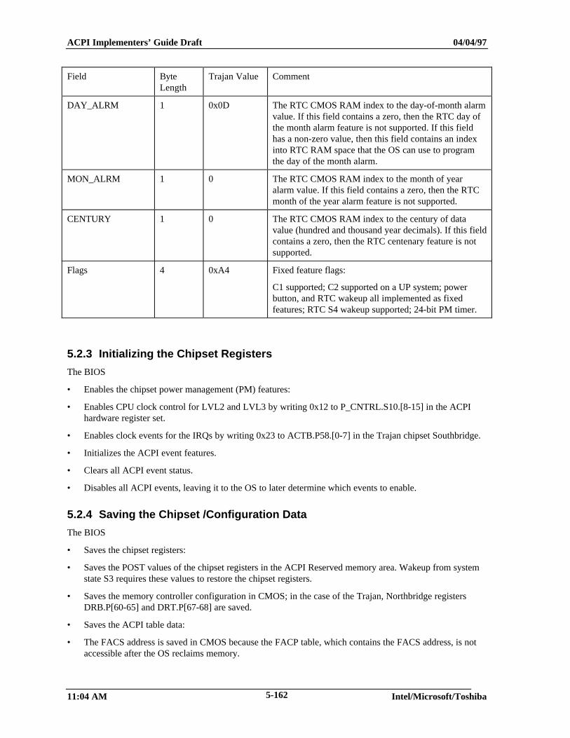
ACPI Implementers’ Guide Draft 04/04/97
11:04 AM Intel/Microsoft/Toshiba5-162
Field ByteLength
Trajan Value Comment
DAY_ALRM 1 0x0D The RTC CMOS RAM index to the day-of-month alarmvalue. If this field contains a zero, then the RTC day ofthe month alarm feature is not supported. If this fieldhas a non-zero value, then this field contains an indexinto RTC RAM space that the OS can use to programthe day of the month alarm.
MON_ALRM 1 0 The RTC CMOS RAM index to the month of yearalarm value. If this field contains a zero, then the RTCmonth of the year alarm feature is not supported.
CENTURY 1 0 The RTC CMOS RAM index to the century of datavalue (hundred and thousand year decimals). If this fieldcontains a zero, then the RTC centenary feature is notsupported.
Flags 4 0xA4 Fixed feature flags:
C1 supported; C2 supported on a UP system; powerbutton, and RTC wakeup all implemented as fixedfeatures; RTC S4 wakeup supported; 24-bit PM timer.
5.2.3 Initializing the Chipset Registers
The BIOS
• Enables the chipset power management (PM) features:
• Enables CPU clock control for LVL2 and LVL3 by writing 0x12 to P_CNTRL.S10.[8-15] in the ACPIhardware register set.
• Enables clock events for the IRQs by writing 0x23 to ACTB.P58.[0-7] in the Trajan chipset Southbridge.
• Initializes the ACPI event features.
• Clears all ACPI event status.
• Disables all ACPI events, leaving it to the OS to later determine which events to enable.
5.2.4 Saving the Chipset /Configuration Data
The BIOS
• Saves the chipset registers:
• Saves the POST values of the chipset registers in the ACPI Reserved memory area. Wakeup from systemstate S3 requires these values to restore the chipset registers.
• Saves the memory controller configuration in CMOS; in the case of the Trajan, Northbridge registersDRB.P[60-65] and DRT.P[67-68] are saved.
• Saves the ACPI table data:
• The FACS address is saved in CMOS because the FACP table, which contains the FACS address, is notaccessible after the OS reclaims memory.
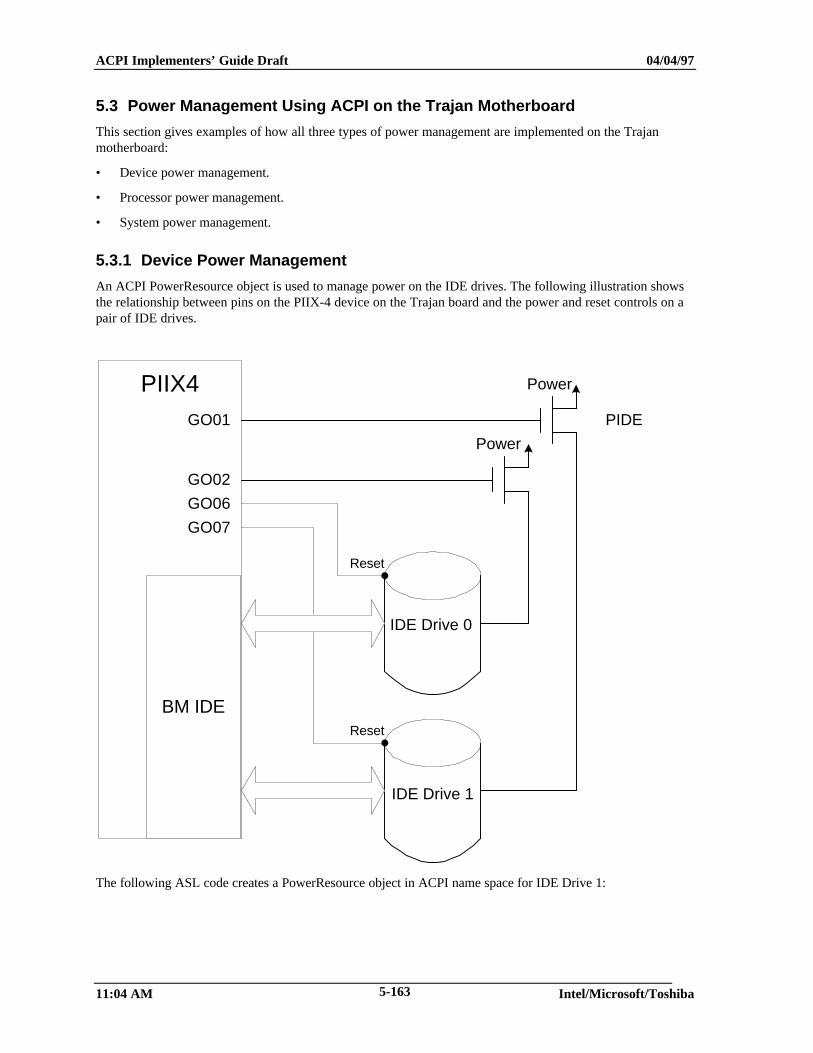
ACPI Implementers’ Guide Draft 04/04/97
11:04 AM Intel/Microsoft/Toshiba5-163
5.3 Power Management Using ACPI on the Trajan Motherboard
This section gives examples of how all three types of power management are implemented on the Trajanmotherboard:
• Device power management.
• Processor power management.
• System power management.
5.3.1 Device Power Management
An ACPI PowerResource object is used to manage power on the IDE drives. The following illustration showsthe relationship between pins on the PIIX-4 device on the Trajan board and the power and reset controls on apair of IDE drives.
BM IDE
IDE Drive 0
IDE Drive 1
GO01
GO02
Power
Power
PIIX4PIDE
GO06
GO07
Reset
Reset
The following ASL code creates a PowerResource object in ACPI name space for IDE Drive 1:
ACPI Implementers’ Guide Draft 04/04/97
11:04 AM Intel/Microsoft/Toshiba5-164
PowerResource(PIDE, 0, 0) { //Power resource for IDE Drive 1//SystemLevel parameter = 0, which means//this IDE drive can be turned off in//any system sleep state.
Method(_STA,0) {Return(XOr(GO01, One)) //Get power status
}Method(_ON){ //
Store(Zero, GO01) //Apply powerSleep(10) //Store(One, GO06) //Pulse resetStall(10) //Store(Zero, GO06) //
} // End Of _ONMethod(_OFF){
Store(One,GO06) //Cut power} // End of _OFF
} // End of Power Resource PIDE
5.3.2 Processor Power Management
Processor power management is accomplished by a combination of the Processor object in ACPI name spaceand the values in the DUTY_OFFSET and DUTY_WIDTH fields in the FACP table. For example, the ASLcode that creates the processor object in the Trajan ACPI name space:Scope(\_PR) { Processor( CPU0, // processor name 1, // unique number for this processor 0x1010, // System IO address of Pblk Registers 0x06 // length in bytes of PBlk ) {} }
Following are the values for the DUTY_OFFSET and DUTY_WIDTH fields in the Trajan ACPI table:
DUTY_OFFSET 1 1 The zero-based index of where the processor’sduty cycle setting is within the processor’sP_CNT register.
DUTY_WIDTH 1 3 The bit width of the processor’s duty cyclesetting value in the P_CNT register.
The value of 1 in the DUTY_OFFSET field of the FACP table indicates that the CLK_VAL value in the ACPIhardware Processor Control (P_CNT) register starts at bit 1. The value of 3 in the DUTY_WIDTH fieldindicates that the CLK_VAL field in P_CNT is 3 bits wide. In other words, bits 1, 2, and 3 of P_CNT are usedfor the CLK_VAL value.
5.3.3 System Power Management
This section describes the role of the ACPI BIOS during transitions into and out of the system working stateS0, and the system sleeping states S1, S2, S3, and S4.
5.3.3.1 The BIOS’s Role in Transitioning Out of the Working State (S0)
The OS has direct access to all the registers it needs to initiate a system sleep state. The OS always runs a\_PTS control method in the ACPI name space at the beginning of each transition to a system sleep state.
An example of one thing that could be done in such a \_PTS method in the Trajan ACPI BIOS would be tosave SMM data changed since POST.
5.3.3.2 The BIOS’s Role in Waking from S1
The BIOS does not get control during the transition from S1 to S0.
ACPI Implementers’ Guide Draft 04/04/97
11:04 AM Intel/Microsoft/Toshiba5-165
Earlier, when the system switched from S0 to S1, no context was lost. So, at the start of the transition from S1back to S0, the clocks are stopped and memory is in suspend refresh, but the chipset is on and the processor ison.
After the OS starts running in the S0 state, it will always run the _WAK control method in the ACPI namespace (passing the value 1 as an argument). An example of what a Trajan BIOS _WAK method could do wheninvoked and passed a value of 1, is:
• Notify the OS to do a “device check” for changes in the docking station (by using the following form ofthe ASL Notify term: Notify(\_SB.PCI0.MPC1, 1).
• Notify the OS to check and set thermal control (by using the following form of the ASL Notify term:Notify(\_TZ.THRM, 0x81).
5.3.3.3 The BIOS’s Role in Waking from S2
Earlier, when the system switched from S0 to S2, the processor was turned off (so all processor context is lost).At the start of the transition from S2 back to S0, the clocks are stopped and memory is in suspend refresh, thechipset is on, and the processor is off.
To start the transition from S2 to S0, the processor starts executing at the power-on reset vector, the processorSMRAM base register is restored, and control is passed to the OS. The OS:
• Gets the FACS table pointer from the CMOS.
• Retrieves the wake vector (a physical memory address) from the FACS table.
• Converts the physical wake vector address to a segment:offset format and starts executing at that address.
After the OS starts running in the S0 state, it will always run the _WAK control method in the ACPI namespace (passing the value of 2 as an argument). An example of what a Trajan BIOS _WAK method could dowhen invoked and passed a value of 2, is:
• Notify the OS to do a “device check” for changes in the docking station (by using the following form ofthe ASL Notify term: Notify(\_SB.PCI0.MPC1, 1).
• Notify the OS to check and set thermal control (by using the following form of the ASL Notify term:Notify(\_TZ.THRM, 0x81).
5.3.3.4 The BIOS’s Role in Waking from S3
Earlier, when the system switched from S0 to S3, the processor was turned off (so all processor context is lost)and the chipset was turned off (so all chipset register contents are lost). At the start of the transition from S3back to S0, the clocks are stopped, and memory is in suspend refresh, the chipset is off, and the processor isoff.
To start the transition from S3 to S0, the processor starts executing at the power-on reset vector, the memorycontroller configuration is restored, the cache is invalidated, the chipset register values are restored from theACPI NVS memory area, the processor SMRAM base register is restored, and control is passed to the OS. TheOS:
• Gets the FACS table pointer from the CMOS.
• Retrieves the wake vector (a physical memory address) from the FACS table.
• Converts the physical wake vector address to a segment:offset format and starts executing at that address.
After the OS starts running in the S0 state, it will always run the _WAK control method in the ACPI namespace (passing the value of 3 as an argument). An example of what a Trajan BIOS _WAK method could dowhen invoked and passed a value of 3, is:
ACPI Implementers’ Guide Draft 04/04/97
11:04 AM Intel/Microsoft/Toshiba5-166
• Notify the OS to do a “device check” for changes in the docking station (by using the following form ofthe ASL Notify term: Notify(\_SB.PCI0.MPC1, 1).
• Notify the OS to check and set thermal control (by using the following form of the ASL Notify term:Notify(\_TZ.THRM, 0x81).
5.3.3.5 The BIOS’s Role in Waking from S4
There are two methods for switching from S0 to S4:
• The BIOS saves memory context to disk, or
• The OS saves and restores memory.
An ACPI-compatible platform specifies the alternative it uses by setting a values in the S4BIOS_REQ field ofthe FACP table. In this case study of the Trajan platform, the S4BIOS_REQ field is set to zero, so the OSsaves and restores memory (for FACP table field values used by this example Trajan platform, see section5.2.2).
For the BIOS, using the OS method to switch from S4 to S0 is the same process as a cold boot (for adescription of the cold boot process, see section 5.2). Note that in waking from S4, the OS makes use of the“hardware signature” value calculated by the BIOS at the previous boot and stored in the FACP table. Thedefinition of the Hardware Signature field in the FACP table is reprinted below from the ACPI Specification,Revision 1.0.
The value of the system’s “hardware signature” at last boot. This value is calculated by the BIOS on a besteffort basis to indicate the base hardware configuration of the system such that different base hardwareconfigurations can have different hardware signature values. The OS uses this information in wakingfrom an S4 state, by comparing the current hardware signature to the signature values saved in the non-volatile sleep image. If the values are not the same, the OS assumes that the saved non-volatile image isfrom a different hardware configuration and can not be restored.
The OS compares the current hardware signature value to the hardware signature value stored in the FACS atlast boot.
• If the two values are the same, the OS restores the contents of conventional memory from the ACPI NVSmemory area.
• If the two values are not the same, the OS does not restore any memory and cold boots the system.
In either case, once the OS starts running in the S0 state, it will always run the _WAK control method in theACPI name space (passing the value of 4 as an argument).
5.4 Plug and Play Using ACPI on the Trajan Motherboard
To enable the OS to successfully carry out device configuration on motherboard devices, an ACPI Deviceobject must be defined in the ACPI name space for each device on the motherboard. This section describes thedevice ID and configuration objects that must be defined under the Device object for
• Single-configuration objects.
• Multiple-configuration objects.
5.4.1 Name Space Objects for Single-Configuration Devices
On the Trajan motherboard, the speaker device on the ISA bus is an example of a device with a singleconfiguration. For such a device, only two objects must be declared under the Device object in the name space:
• _HID, which reports the device Plug and Play ID
ACPI Implementers’ Guide Draft 04/04/97
11:04 AM Intel/Microsoft/Toshiba5-167
• _CRS, which reports the device’s single configuration.
The following sample ASL code illustrates this:Device(SPKR) { // Device object name is ‘SPKR’
Name(_HID,EISAID("PNP0800")) // Hardware Device ID for speaker className(_CRS,Buffer(){
0x47, // IO port type of resource descriptor0x01, // Decodes 16-bit addresses0x61, // Bits [7:0] of minimum base I/O address SPKR can be configured for0x00, // Bits [15:8] of minimum base I/O address0x61, // Bits [7:0] of maximum base I/O address SPKR can be configured for0x00, // Bits [15:8] of maximum base I/O address0x01, // Base alignment0x01, // Number of contiguous I/O ports requested0x79, // End tag0x00} // end of Buffer
) // end of _CRS} // end of SPKR device
5.4.2 Name Space Objects for Multiple-Configuration Devices
On the Trajan motherboard, the floppy disk controller in the Super IO chip is an example of a device withmultiple configurations. For such a device, these objects and control methods need to be implemented underthe Device object in the name space:
• _HID, which reports the device Plug and Play ID
• _CRS, which reports the device’s current configuration.
• _PRS, which reports the device’s possible configurations.
• _SRS, which sets the device’s current configuration.
• _STA, which reports the device’s current status (enabled and decoding hardware resources or disabledand not decoding hardware resources, functioning properly or failed its diagnostics, and so on).
• _DIS, which disables the device (called after the OS sets the device to a D3 device power state).
5.4.3 Field Declarations
ASL OperationRegion and Field terms (not shown) declare the following named fields for use by the _CRS,_SRS, _STA, and _DIS control methods that go under the Device object for the floppy disk controller in thename space hierarchy:
• ‘FER’ is a SuperIO chip register that contains the FDC enable bit.
• ‘F0AD’ is a field in the chipset register RESB that selects the FDC IO address.
• ‘F0EN’ is a field in the chipset register RESB that enables the decoding of the selected IOaddress.
5.4.4 Example _CRS, _SRS, _STA, and _DIS Methods for the FDC
The following sample ASL code illustrates this for the floppy disk controller on the example Trajanmotherboard:
ACPI Implementers’ Guide Draft 04/04/97
11:04 AM Intel/Microsoft/Toshiba5-168
Device(FDC0) { // Floppy Disk Controller (FDC)Name(_HID, EISAID("PNP0700")) // PnP Device ID
Method(_CRS,0){ //Current Resource Setting for FDCName(BUF0,Buffer(){
//IO port descriptor, 16-bit decode, IO port 370-3770x47, 0x01, 0x70, 0x03, 0x70, 0x03, 0x01, 0x08,//IRQ descriptor, edge, IRQ60x22, 0x40, 0x00,//DMA descriptor, channel 2, ISA compatible0x2A, 0x04, 0x00,//End tag0x79, 0x00}
)CreateByteField(BUF0, 0x02, IOLL) //Low byte of min portCreateByteField(BUF0, 0x04, IOHL) //Low byte of max portAnd(FER, 0x20, local0) //Check FDC select bitIf(LEqual(Local0,Zero)) { //Primary FDC selected
Store(0xF0,IOLL) //Change port addressStore(0xF0, IOHL)}
Return(BUF0)} //End _CRS method
.
.
.Method(_SRS,1){ //Set Resource
//Arg0 contains PnP resource string passed in from the OSCreateWordField(Arg0, 0x02, IOAR) //IOAR points to portAnd(FER, 0xD7, Local0) //Assume primary FDCStore(Zero, Local1)If(LEqual(IOAR, 0x370)){ //If OS selects secondary FDC
Or(Local0, 0x20, Local0) //Change for secondary FDCStore(One, Local1)
Store(Local1, PCI0.PX43.RESB.F0AD) //Set FDC addressStore(One, PCI0.PX43.RESB.F0EN) //Enable FDC decodeOr(Local0, 0x08, Local0) //Enable FDCStore(Local0, FER)Store(Local0, DAT)
} // end of _SRS method
Method(_STA,0){ // Status of the FDCAnd(FER, 0x08, Local0) // Check FDC enable bitIf(Local0)
{Return(0x0B)} // Present, enabled, and functioningElse
{Return(0x01)} // Present, but disabled} //end _STA method
Method(_DIS,0){ // Disable FDCAnd(FER, 0xF7, Local0)Store(Local0, FER)Store(Local0, DAT) // Need two writes to data port!Store(Zero, PCI0.PX43.RESB.F0EN) // Disable decode
} //end _DIS method} // end of FDC0 device
5.5 Docking Using ACPI on the Trajan Motherboard
To enable the OS to successfully manage devices inserted into and removed from a docking station, an ACPIDevice object must be declared for the Dock in the ACPI name space. Under the Device object representing theDock,
• Device configuration objects must be used.
• Device insertion and removal objects must be used (for example, _EJx).
• The _UID device identification method may need to be used to report the unique dock serial number.
The interface with the OS is accomplished using ASL synchronization and notification terms.
This section illustrates these ideas with example ASL code for the Trajan example platform.
ACPI Implementers’ Guide Draft 04/04/97
11:04 AM Intel/Microsoft/Toshiba5-169
5.5.1 Field Declarations
ASL OperationRegion and Field terms (not shown) declare the following named fields:
• ‘OPEN’ is a field in the docking chipset registers (OPENREQ.P41.0) that is an undock request.
• ‘DOCK’ is a field in the docking chipset registers (DOCKED.P41.1) that reports system docked.
• ‘UDKP’ is a field in the docking chipset registers (UDKPERMIT.P41.3) that reports whether anundock request is permitted.
• ‘QENx’ names a set of fields in the docking chipset registers (QvccENx.P40.[2-3]) that are Qbuffer enables.
• ‘MIEN’ is a field that reports whether a PCI-ISA bridge is present.
ACPI Implementers’ Guide Draft 04/04/97
11:04 AM Intel/Microsoft/Toshiba5-170
5.5.2 Example _ADR, _UID, _EJ0, and Device Objects for the Dock
Device(MPCI) { //Docking stationName(_ADR, 0x00110000) //Bridge is Dev 17 on PCI bus 0Name(_UID, 1) //Unique ID is 1Method(_EJ0, 1){ //Hot docking support
//Arg0: 0=insert, 1=ejectIf(Arg0) { //Eject
Store(One, UDKP) //Start undock sequenceWait(EJT0, 0xFFFF) //Wait for signal from OSReturn(0)}
Else{}} //Insert, nothing to do//Declare Device objects for all devices behind docking hereDevice(MISA) {
.
.
.} //End device MISADevice(DIDE) {
.
.
.} //End device DIDE
.
.
.} //End device MPCI
5.5.3 Example Synchronization and NotificationsMutex(EJT0, 16) //Declare synchronization objectScope(_GPE) {
Method(_L09) {// Get docking statusXOr(OPEN, 0x01, Local1) //Undock request invertedXOr(DOCK, 0x01, Local2) //System docked report invertedXOr(UDKP, 0x01, Local3) //Undock request permitted report invertedIf(Local1) { //This is an undock request
Store(Zero, OPEN) //Clear status bitNotify(\_SB.PCI0.MPCI, 1) //Notify OS of event on MPCI (Dock) device object
//1 = Ejection Request}
Else {If(Local2) { //This is a station docked eventStore(One, QEN1) //Turn on Q buffersStore(One, QEN2)Store(One, MIEN) //Enable ISA busNotify(\_SB.PCI0.MPCI, 0) //Notify OS of event on MPCI (Dock) device object
//0 = Device Check}
Else {If(Local3) { //Start undock sequenceStore(Zero, QEN1) //Turn off Q buffersStore(Zero, QEN2)Store(Zero, UDKP) //Undock sequence starts hereStall(200) //Give chipset time to finish,Stall(100) //No blockingSignal(EJT0) //Release synchronization object}}
}}
5.6 Switching Between ACPI and Legacy Modes on the Trajan Motherboard
The OS switches a platform between ACPI and legacy modes by writing values to the SMI command(SMI_CMD) port. The system port address of the SMI command port for a particular platform is in theSMI_CMD field of the FACP table (for example, the SMI_CMD system port address for this example Trajanplatform is 0xB2; see section 5.2.2).
ACPI Implementers’ Guide Draft 04/04/97
11:04 AM Intel/Microsoft/Toshiba5-171
• On platforms that support both ACPI and legacy modes, as well as on platforms that support ACPI-only,the OS writes the value ACPI_ENABLE to the SMI_CMD port address to switch to ACPI mode.
• On platforms that support both ACPI and legacy modes, the OS writes ACPI_DISABLE to the SMI_CMDport address to switch to legacy mode.
5.6.1 Switching From Legacy to ACPI Mode
When switching from legacy to ACPI mode, the BIOS
1. Saves all power management-related chipset registers (such as idle, traps, timers, and so on) in SMRAM.
2. Disables all legacy PM timers.
3. Disables all ACPI events so the OS can select the events that match its policies.
4. Sets the SCI_EN bit in the ACPI hardware register.
5.6.2 Switching From ACPI to Legacy Mode
When switching from ACPI to legacy mode, the BIOS
• Restores the power-management related registers from SMRAM; this puts idles, traps, timers, and so onback to their original states.
• Resets the SCI_EN bit in the ACPI hardware register.

ACPI Implementers’ Guide Draft 04/04/97
11:04 AM Intel/Microsoft/Toshiba5-172
.
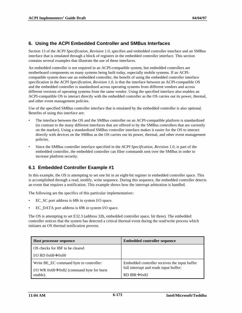
ACPI Implementers’ Guide Draft 04/04/97
11:04 AM Intel/Microsoft/Toshiba6-173
6. Using the ACPI Embedded Controller and SMBus Interfaces
Section 13 of the ACPI Specification, Revision 1.0, specifies and embedded controller interface and an SMBusinterface that is emulated through a block of registers in the embedded controller interface. This sectioncontains several examples that illustrate the use of these interfaces.
An embedded controller is not required in an ACPI-compatible system, but embedded controllers aremotherboard components on many systems being built today, especially mobile systems. If an ACPI-compatible system does use an embedded controller, the benefit of using the embedded controller interfacespecification in the ACPI Specification, Revision 1.0, is that the interface between an ACPI-compatible OSand the embedded controller is standardized across operating systems from different vendors and acrossdifferent versions of operating systems from the same vendor. Using the specified interface also enables anACPI-compatible OS to interact directly with the embedded controller as the OS carries out its power, thermal,and other event management policies.
Use of the specified SMBus controller interface that is emulated by the embedded controller is also optional.Benefits of using this interface are:
• The interface between the OS and the SMBus controller on an ACPI-compatible platform is standardized(in contrast to the many different interfaces that are offered to by the SMBus controllers that are currentlyon the market). Using a standardized SMBus controller interface makes it easier for the OS to interactdirectly with devices on the SMBus as the OS carries out its power, thermal, and other event managementpolicies.
• Since the SMBus controller interface specified in the ACPI Specification, Revision 1.0, is part of theembedded controller, the embedded controller can filter commands sent over the SMBus in order toincrease platform security.
6.1 Embedded Controller Example #1
In this example, the OS is attempting to set one bit in an eight-bit register in embedded controller space. Thisis accomplished through a read, modify, write sequence. During this sequence, the embedded controller detectsan event that requires a notification. This example shows how the interrupt arbitration is handled.
The following are the specifics of this particular implementation::
• EC_SC port address is 68h in system I/O space.
• EC_DATA port address is 69h in system I/O space.
The OS is attempting to set E32.3 (address 32h, embedded controller space, bit three). The embeddedcontroller notices that the system has detected a critical thermal event during the read/write process whichinitiates an OS thermal notification process.
Host processor sequence Embedded controller sequence
OS checks for IBF to be cleared
I/O RD 0x68à0x00
Write BE_EC command byte to controller:
I/O WR 0x68à0x82 (command byte for burstenable).
Embedded controller receives the input bufferfull interrupt and reads input buffer:
RD IBRà0x82
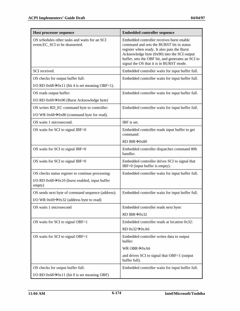
ACPI Implementers’ Guide Draft 04/04/97
11:04 AM Intel/Microsoft/Toshiba6-174
Host processor sequence Embedded controller sequence
OS schedules other tasks and waits for an SCIevent.EC_SCI to be deasserted.
Embedded controller receives burst enablecommand and sets the BURST bit in statusregister when ready. It also puts the BurstAcknowledge byte (0x90) into the SCI outputbuffer, sets the OBF bit, and generates an SCI tosignal the OS that it is in BURST mode.
SCI received. Embedded controller waits for input buffer full.
OS checks for output buffer full:
I/O RD 0x68à0x11 (bit 4 is set meaning OBF=1).
Embedded controller waits for input buffer full.
OS reads output buffer:
I/O RD 0x69à0x90 (Burst Acknowledge byte)
Embedded controller waits for input buffer full.
OS writes RD_EC command byte to controller:
I/O WR 0x68à0x80 (command byte for read).
Embedded controller waits for input buffer full.
OS waits 1 microsecond. IBF is set.
OS waits for SCI to signal IBF=0 Embedded controller reads input buffer to getcommand:
RD IBRà0x80
OS waits for SCI to signal IBF=0 Embedded controller dispatches command 80hhandler.
OS waits for SCI to signal IBF=0 Embedded controller drives SCI to signal thatIBF=0 (input buffer is empty).
OS checks status register to continue processing:
I/O RD 0x68à0x10 (burst enabled, input bufferempty)
Embedded controller waits for input buffer full.
OS sends next byte of command sequence (address):
I/O WR 0x69à0x32 (address byte to read)
Embedded controller waits for input buffer full.
OS waits 1 microsecond Embedded controller reads next byte:
RD IBRà0x32
OS waits for SCI to signal OBF=1 Embedded controller reads at location 0x32:
RD 0x32à0xA6
OS waits for SCI to signal OBF=1 Embedded controller writes data to outputbuffer:
WR OBRà0xA6
and drives SCI to signal that OBF=1 (outputbuffer full).
OS checks for output buffer full:
I/O RD 0x68à0x11 (bit 0 is set meaning OBF)
Embedded controller waits for input buffer full.
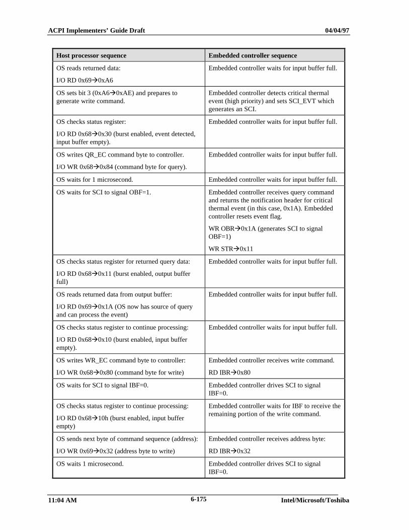
ACPI Implementers’ Guide Draft 04/04/97
11:04 AM Intel/Microsoft/Toshiba6-175
Host processor sequence Embedded controller sequence
OS reads returned data:
I/O RD 0x69à0xA6
Embedded controller waits for input buffer full.
OS sets bit 3 (0xA6à0xAE) and prepares togenerate write command.
Embedded controller detects critical thermalevent (high priority) and sets SCI_EVT whichgenerates an SCI.
OS checks status register:
I/O RD 0x68à0x30 (burst enabled, event detected,input buffer empty).
Embedded controller waits for input buffer full.
OS writes QR_EC command byte to controller.
I/O WR 0x68à0x84 (command byte for query).
Embedded controller waits for input buffer full.
OS waits for 1 microsecond. Embedded controller waits for input buffer full.
OS waits for SCI to signal OBF=1. Embedded controller receives query commandand returns the notification header for criticalthermal event (in this case, 0x1A). Embeddedcontroller resets event flag.
WR OBRà0x1A (generates SCI to signalOBF=1)
WR STRà0x11
OS checks status register for returned query data:
I/O RD 0x68à0x11 (burst enabled, output bufferfull)
Embedded controller waits for input buffer full.
OS reads returned data from output buffer:
I/O RD 0x69à0x1A (OS now has source of queryand can process the event)
Embedded controller waits for input buffer full.
OS checks status register to continue processing:
I/O RD 0x68à0x10 (burst enabled, input bufferempty).
Embedded controller waits for input buffer full.
OS writes WR_EC command byte to controller:
I/O WR 0x68à0x80 (command byte for write)
Embedded controller receives write command.
RD IBRà0x80
OS waits for SCI to signal IBF=0. Embedded controller drives SCI to signalIBF=0.
OS checks status register to continue processing:
I/O RD 0x68à10h (burst enabled, input bufferempty)
Embedded controller waits for IBF to receive theremaining portion of the write command.
OS sends next byte of command sequence (address):
I/O WR 0x69à0x32 (address byte to write)
Embedded controller receives address byte:
RD IBRà0x32
OS waits 1 microsecond. Embedded controller drives SCI to signalIBF=0.
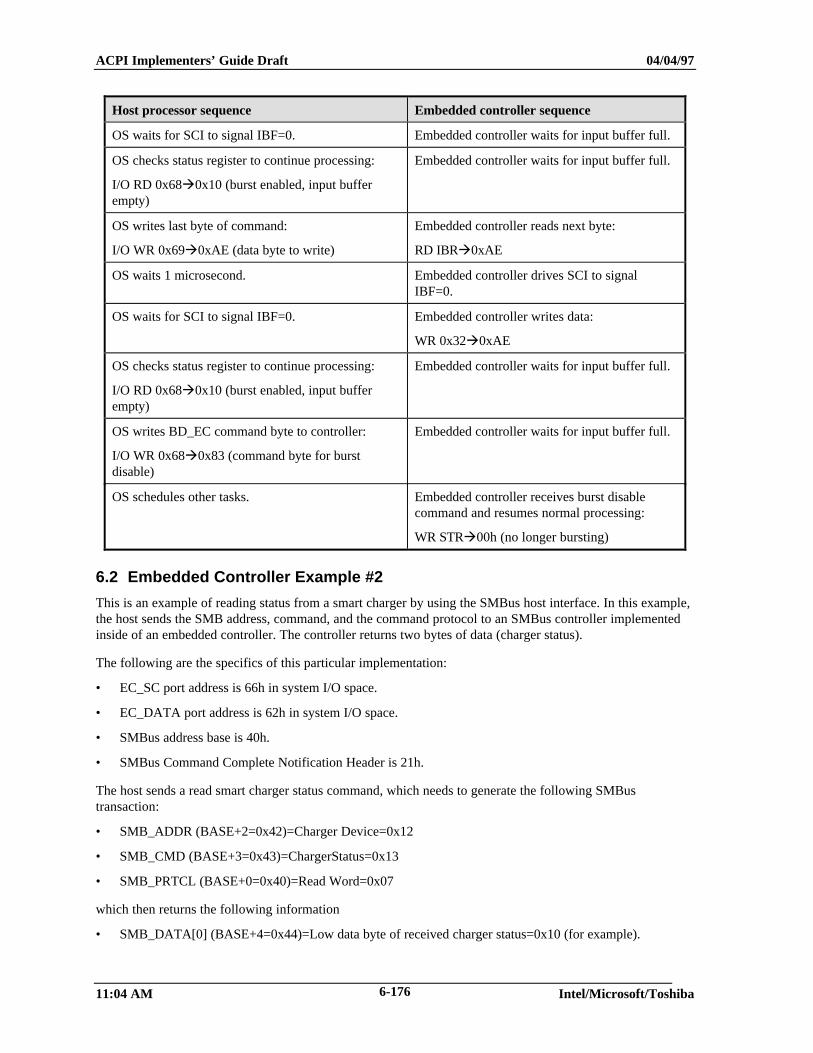
ACPI Implementers’ Guide Draft 04/04/97
11:04 AM Intel/Microsoft/Toshiba6-176
Host processor sequence Embedded controller sequence
OS waits for SCI to signal IBF=0. Embedded controller waits for input buffer full.
OS checks status register to continue processing:
I/O RD 0x68à0x10 (burst enabled, input bufferempty)
Embedded controller waits for input buffer full.
OS writes last byte of command:
I/O WR 0x69à0xAE (data byte to write)
Embedded controller reads next byte:
RD IBRà0xAE
OS waits 1 microsecond. Embedded controller drives SCI to signalIBF=0.
OS waits for SCI to signal IBF=0. Embedded controller writes data:
WR 0x32à0xAE
OS checks status register to continue processing:
I/O RD 0x68à0x10 (burst enabled, input bufferempty)
Embedded controller waits for input buffer full.
OS writes BD_EC command byte to controller:
I/O WR 0x68à0x83 (command byte for burstdisable)
Embedded controller waits for input buffer full.
OS schedules other tasks. Embedded controller receives burst disablecommand and resumes normal processing:
WR STRà00h (no longer bursting)
6.2 Embedded Controller Example #2
This is an example of reading status from a smart charger by using the SMBus host interface. In this example,the host sends the SMB address, command, and the command protocol to an SMBus controller implementedinside of an embedded controller. The controller returns two bytes of data (charger status).
The following are the specifics of this particular implementation:
• EC_SC port address is 66h in system I/O space.
• EC_DATA port address is 62h in system I/O space.
• SMBus address base is 40h.
• SMBus Command Complete Notification Header is 21h.
The host sends a read smart charger status command, which needs to generate the following SMBustransaction:
• SMB_ADDR (BASE+2=0x42)=Charger Device=0x12
• SMB_CMD (BASE+3=0x43)=ChargerStatus=0x13
• SMB_PRTCL (BASE+0=0x40)=Read Word=0x07
which then returns the following information
• SMB_DATA[0] (BASE+4=0x44)=Low data byte of received charger status=0x10 (for example).
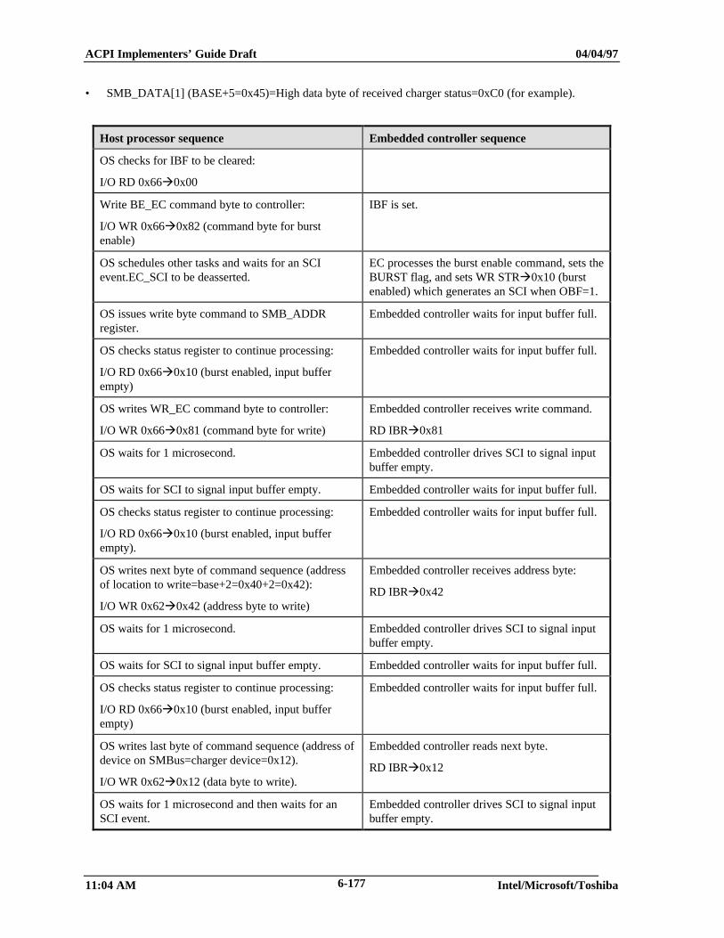
ACPI Implementers’ Guide Draft 04/04/97
11:04 AM Intel/Microsoft/Toshiba6-177
• SMB_DATA[1] (BASE+5=0x45)=High data byte of received charger status=0xC0 (for example).
Host processor sequence Embedded controller sequence
OS checks for IBF to be cleared:
I/O RD 0x66à0x00
Write BE_EC command byte to controller:
I/O WR 0x66à0x82 (command byte for burstenable)
IBF is set.
OS schedules other tasks and waits for an SCIevent.EC_SCI to be deasserted.
EC processes the burst enable command, sets theBURST flag, and sets WR STRà0x10 (burstenabled) which generates an SCI when OBF=1.
OS issues write byte command to SMB_ADDRregister.
Embedded controller waits for input buffer full.
OS checks status register to continue processing:
I/O RD 0x66à0x10 (burst enabled, input bufferempty)
Embedded controller waits for input buffer full.
OS writes WR_EC command byte to controller:
I/O WR 0x66à0x81 (command byte for write)
Embedded controller receives write command.
RD IBRà0x81
OS waits for 1 microsecond. Embedded controller drives SCI to signal inputbuffer empty.
OS waits for SCI to signal input buffer empty. Embedded controller waits for input buffer full.
OS checks status register to continue processing:
I/O RD 0x66à0x10 (burst enabled, input bufferempty).
Embedded controller waits for input buffer full.
OS writes next byte of command sequence (addressof location to write=base+2=0x40+2=0x42):
I/O WR 0x62à0x42 (address byte to write)
Embedded controller receives address byte:
RD IBRà0x42
OS waits for 1 microsecond. Embedded controller drives SCI to signal inputbuffer empty.
OS waits for SCI to signal input buffer empty. Embedded controller waits for input buffer full.
OS checks status register to continue processing:
I/O RD 0x66à0x10 (burst enabled, input bufferempty)
Embedded controller waits for input buffer full.
OS writes last byte of command sequence (address ofdevice on SMBus=charger device=0x12).
I/O WR 0x62à0x12 (data byte to write).
Embedded controller reads next byte.
RD IBRà0x12
OS waits for 1 microsecond and then waits for anSCI event.
Embedded controller drives SCI to signal inputbuffer empty.
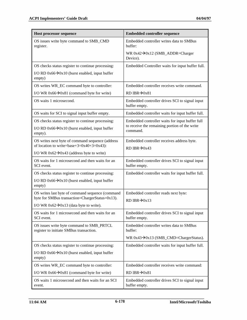
ACPI Implementers’ Guide Draft 04/04/97
11:04 AM Intel/Microsoft/Toshiba6-178
Host processor sequence Embedded controller sequence
OS issues write byte command to SMB_CMDregister.
Embedded controller writes data to SMBusbuffer:
WR 0x42à0x12 (SMB_ADDR=ChargerDevice).
OS checks status register to continue processing:
I/O RD 0x66à0x10 (burst enabled, input bufferempty)
Embedded Controller waits for input buffer full.
OS writes WR_EC command byte to controller:
I/O WR 0x66à0x81 (command byte for write)
Embedded controller receives write command.
RD IBRà0x81
OS waits 1 microsecond. Embedded controller drives SCI to signal inputbuffer empty.
OS waits for SCI to signal input buffer empty. Embedded controller waits for input buffer full.
OS checks status register to continue processing:
I/O RD 0x66à0x10 (burst enabled, input bufferempty).
Embedded controller waits for input buffer fullto receive the remaining portion of the writecommand.
OS writes next byte of command sequence (addressof location to write=base+3=0x40+3=0x43):
I/O WR 0x62à0x43 (address byte to write)
Embedded controller receives address byte.
RD IBRà0x43
OS waits for 1 microsecond and then waits for anSCI event.
Embedded controller drives SCI to signal inputbuffer empty.
OS checks status register to continue processing:
I/O RD 0x66à0x10 (burst enabled, input bufferempty)
Embedded controller waits for input buffer full.
OS writes last byte of command sequence (commandbyte for SMBus transaction=ChargerStatus=0x13).
I/O WR 0x62à0x13 (data byte to write).
Embedded controller reads next byte:
RD IBRà0x13
OS waits for 1 microsecond and then waits for anSCI event.
Embedded controller drives SCI to signal inputbuffer empty.
OS issues write byte command to SMB_PRTCLregister to initiate SMBus transaction.
Embedded controller writes data to SMBusbuffer:
WR 0x43à0x13 (SMB_CMD=ChargerStatus).
OS checks status register to continue processing:
I/O RD 0x66à0x10 (burst enabled, input bufferempty)
Embedded controller waits for input buffer full.
OS writes WR_EC command byte to controller:
I/O WR 0x66à0x81 (command byte for write)
Embedded controller receives write command:
RD IBRà0x81
OS waits 1 microsecond and then waits for an SCIevent.
Embedded controller drives SCI to signal inputbuffer empty.
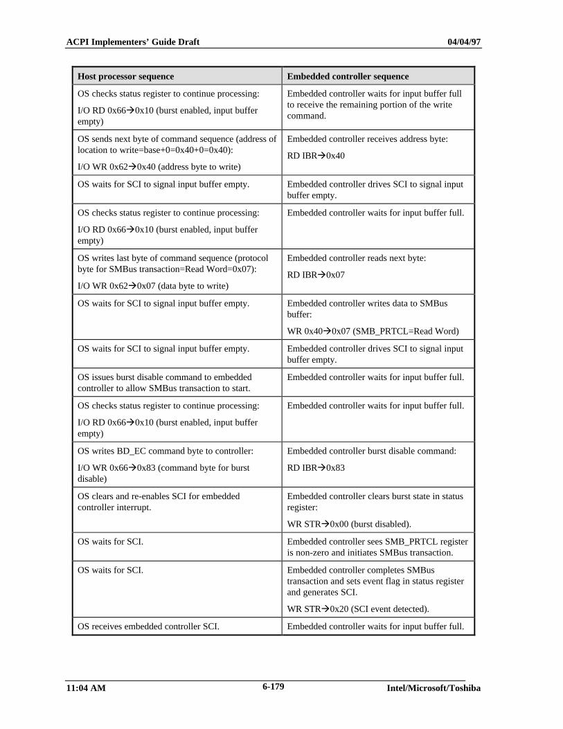
ACPI Implementers’ Guide Draft 04/04/97
11:04 AM Intel/Microsoft/Toshiba6-179
Host processor sequence Embedded controller sequence
OS checks status register to continue processing:
I/O RD 0x66à0x10 (burst enabled, input bufferempty)
Embedded controller waits for input buffer fullto receive the remaining portion of the writecommand.
OS sends next byte of command sequence (address oflocation to write=base+0=0x40+0=0x40):
I/O WR 0x62à0x40 (address byte to write)
Embedded controller receives address byte:
RD IBRà0x40
OS waits for SCI to signal input buffer empty. Embedded controller drives SCI to signal inputbuffer empty.
OS checks status register to continue processing:
I/O RD 0x66à0x10 (burst enabled, input bufferempty)
Embedded controller waits for input buffer full.
OS writes last byte of command sequence (protocolbyte for SMBus transaction=Read Word=0x07):
I/O WR 0x62à0x07 (data byte to write)
Embedded controller reads next byte:
RD IBRà0x07
OS waits for SCI to signal input buffer empty. Embedded controller writes data to SMBusbuffer:
WR 0x40à0x07 (SMB_PRTCL=Read Word)
OS waits for SCI to signal input buffer empty. Embedded controller drives SCI to signal inputbuffer empty.
OS issues burst disable command to embeddedcontroller to allow SMBus transaction to start.
Embedded controller waits for input buffer full.
OS checks status register to continue processing:
I/O RD 0x66à0x10 (burst enabled, input bufferempty)
Embedded controller waits for input buffer full.
OS writes BD_EC command byte to controller:
I/O WR 0x66à0x83 (command byte for burstdisable)
Embedded controller burst disable command:
RD IBRà0x83
OS clears and re-enables SCI for embeddedcontroller interrupt.
Embedded controller clears burst state in statusregister:
WR STRà0x00 (burst disabled).
OS waits for SCI. Embedded controller sees SMB_PRTCL registeris non-zero and initiates SMBus transaction.
OS waits for SCI. Embedded controller completes SMBustransaction and sets event flag in status registerand generates SCI.
WR STRà0x20 (SCI event detected).
OS receives embedded controller SCI. Embedded controller waits for input buffer full.
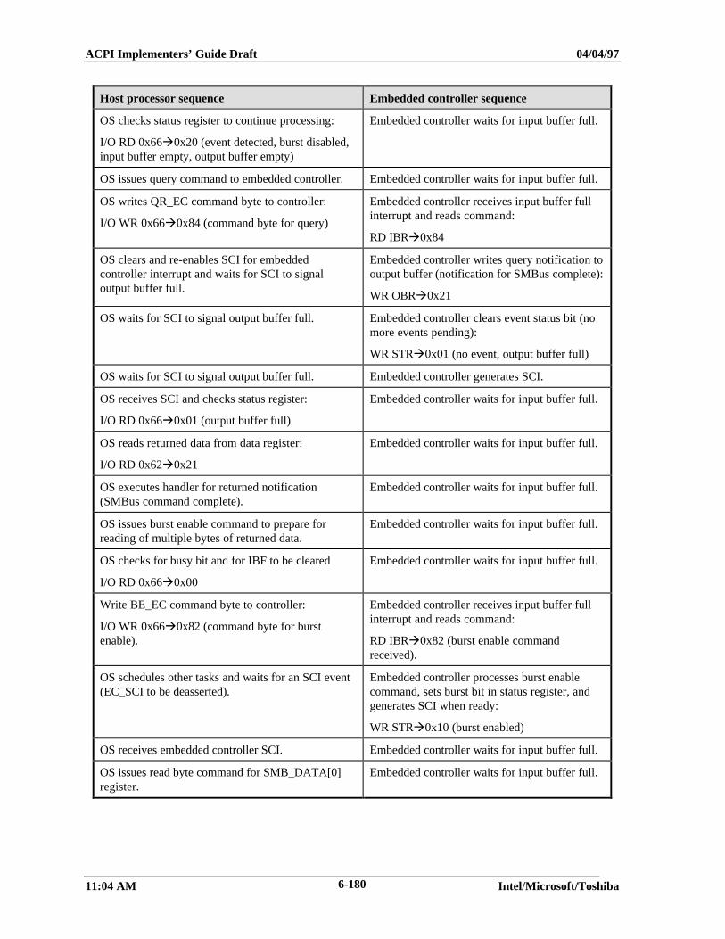
ACPI Implementers’ Guide Draft 04/04/97
11:04 AM Intel/Microsoft/Toshiba6-180
Host processor sequence Embedded controller sequence
OS checks status register to continue processing:
I/O RD 0x66à0x20 (event detected, burst disabled,input buffer empty, output buffer empty)
Embedded controller waits for input buffer full.
OS issues query command to embedded controller. Embedded controller waits for input buffer full.
OS writes QR_EC command byte to controller:
I/O WR 0x66à0x84 (command byte for query)
Embedded controller receives input buffer fullinterrupt and reads command:
RD IBRà0x84
OS clears and re-enables SCI for embeddedcontroller interrupt and waits for SCI to signaloutput buffer full.
Embedded controller writes query notification tooutput buffer (notification for SMBus complete):
WR OBRà0x21
OS waits for SCI to signal output buffer full. Embedded controller clears event status bit (nomore events pending):
WR STRà0x01 (no event, output buffer full)
OS waits for SCI to signal output buffer full. Embedded controller generates SCI.
OS receives SCI and checks status register:
I/O RD 0x66à0x01 (output buffer full)
Embedded controller waits for input buffer full.
OS reads returned data from data register:
I/O RD 0x62à0x21
Embedded controller waits for input buffer full.
OS executes handler for returned notification(SMBus command complete).
Embedded controller waits for input buffer full.
OS issues burst enable command to prepare forreading of multiple bytes of returned data.
Embedded controller waits for input buffer full.
OS checks for busy bit and for IBF to be cleared
I/O RD 0x66à0x00
Embedded controller waits for input buffer full.
Write BE_EC command byte to controller:
I/O WR 0x66à0x82 (command byte for burstenable).
Embedded controller receives input buffer fullinterrupt and reads command:
RD IBRà0x82 (burst enable commandreceived).
OS schedules other tasks and waits for an SCI event(EC_SCI to be deasserted).
Embedded controller processes burst enablecommand, sets burst bit in status register, andgenerates SCI when ready:
WR STRà0x10 (burst enabled)
OS receives embedded controller SCI. Embedded controller waits for input buffer full.
OS issues read byte command for SMB_DATA[0]register.
Embedded controller waits for input buffer full.
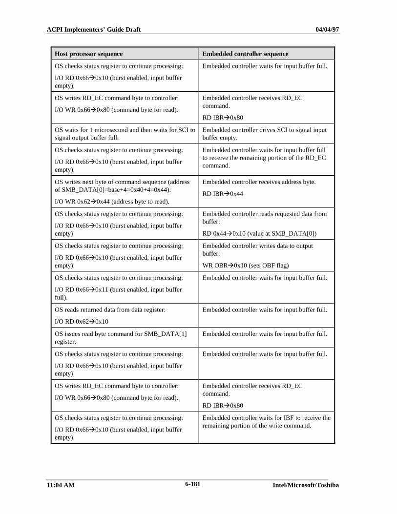
ACPI Implementers’ Guide Draft 04/04/97
11:04 AM Intel/Microsoft/Toshiba6-181
Host processor sequence Embedded controller sequence
OS checks status register to continue processing:
I/O RD 0x66à0x10 (burst enabled, input bufferempty).
Embedded controller waits for input buffer full.
OS writes RD_EC command byte to controller:
I/O WR 0x66à0x80 (command byte for read).
Embedded controller receives RD_ECcommand.
RD IBRà0x80
OS waits for 1 microsecond and then waits for SCI tosignal output buffer full.
Embedded controller drives SCI to signal inputbuffer empty.
OS checks status register to continue processing:
I/O RD 0x66à0x10 (burst enabled, input bufferempty).
Embedded controller waits for input buffer fullto receive the remaining portion of the RD_ECcommand.
OS writes next byte of command sequence (addressof SMB_DATA[0]=base+4=0x40+4=0x44):
I/O WR 0x62à0x44 (address byte to read).
Embedded controller receives address byte.
RD IBRà0x44
OS checks status register to continue processing:
I/O RD 0x66à0x10 (burst enabled, input bufferempty)
Embedded controller reads requested data frombuffer:
RD 0x44à0x10 (value at SMB_DATA[0])
OS checks status register to continue processing:
I/O RD 0x66à0x10 (burst enabled, input bufferempty).
Embedded controller writes data to outputbuffer:
WR OBRà0x10 (sets OBF flag)
OS checks status register to continue processing:
I/O RD 0x66à0x11 (burst enabled, input bufferfull).
Embedded controller waits for input buffer full.
OS reads returned data from data register:
I/O RD 0x62à0x10
Embedded controller waits for input buffer full.
OS issues read byte command for SMB_DATA[1]register.
Embedded controller waits for input buffer full.
OS checks status register to continue processing:
I/O RD 0x66à0x10 (burst enabled, input bufferempty)
Embedded controller waits for input buffer full.
OS writes RD_EC command byte to controller:
I/O WR 0x66à0x80 (command byte for read).
Embedded controller receives RD_ECcommand.
RD IBRà0x80
OS checks status register to continue processing:
I/O RD 0x66à0x10 (burst enabled, input bufferempty)
Embedded controller waits for IBF to receive theremaining portion of the write command.
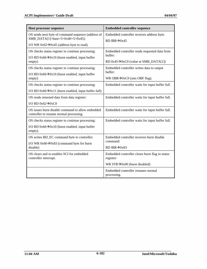
ACPI Implementers’ Guide Draft 04/04/97
11:04 AM Intel/Microsoft/Toshiba6-182
Host processor sequence Embedded controller sequence
OS sends next byte of command sequence (address ofSMB_DATA[1]=base+5=0x40+5=0x45):
I/O WR 0x62à0x45 (address byte to read).
Embedded controller receives address byte:
RD IBRà0x45
OS checks status register to continue processing:
I/O RD 0x66à0x10 (burst enabled, input bufferempty)
Embedded controller reads requested data frombuffer:
RD 0x45à0xC0 (value at SMB_DATA[1])
OS checks status register to continue processing:
I/O RD 0x66à0x10 (burst enabled, input bufferempty)
Embedded controller writes data to outputbuffer:
WR OBRà0xC0 (sets OBF flag).
OS checks status register to continue processing:
I/O RD 0x66à0x11 (burst enabled, input buffer full)
Embedded controller waits for input buffer full.
OS reads returned data from data register:
I/O RD 0x62à0xC0
Embedded controller waits for input buffer full.
OS issues burst disable command to allow embeddedcontroller to resume normal processing.
Embedded controller waits for input buffer full.
OS checks status register to continue processing:
I/O RD 0x66à0x10 (burst enabled, input bufferempty).
Embedded controller waits for input buffer full.
OS writes BD_EC command byte to controller:
I/O WR 0x66à0x83 (command byte for burstdisable)
Embedded controller receives burst disablecommand:
RD IBRà0x83
OS clears and re-enables SCI for embeddedcontroller interrupt.
Embedded controller clears burst flag in statusregister:
WR STRà0x00 (burst disabled)
Embedded controller resumes normalprocessing.
ACPI Implementers’ Guide Draft 04/04/97
11:04 AM Intel/Microsoft/Toshiba7-183
7. Appendix - Suggested Validation and Test Procedures
This section suggests a five-step procedure that gets ACPI-compatible hardware and firmware running underan ACPI-compatible OS. The five-step procedure is a general one, it is a suggested way to systematically proveout your ACPI-compatible hardware and firmware on any ACPI-compatible OS. In the description of the stepsthat follows, some steps are illustrated using a particular ACPI-compatible OS -- the Memphis version ofWindows.
The five-step procedure is:
1. This step can be accomplished before you install an ACPI-compatible OS on your ACPI hardwareplatform. Double check your ACPI tables, ACPI name space, and INT 15h E820, E801, and 88 functioncalls for compliance with the ACPI Specification, Version 1.0. Get the common mistakes out of yourACPI tables, ACPI name space, and use the INT 15h E820, E801, and 88 function calls.
2. Install an ACPI-compatible OS on your ACPI-compatible hardware platform, along with your firmware(ACPI BIOS), and then achieve a successful boot.
3. Successfully exercise the ACPI functionality running your ACPI-compatible platform under the ACPI-compatible OS.
4. Successfully exercise the overall functionality of the ACPI-compatible OS/ACPI system.
5. Install an add-on device and its device driver that implements the ACPI-compatible Dx power states andsuccessfully exercise that device. Success means the Dx-aware driver, the ACPI-compatible OS, and yourACPI tables are all working together.
7.1 Step 1: Static Checking of ACPI Tables, Namespace, and INT 15hFunctions
This step can be accomplished before you install an ACPI-compatible OS on your ACPI hardware platform.
7.1.1 Double-checking for Specification Compliance
Section 5.2 of the ACPI Specification, Revision 1.0, specifies the structure and content of the ACPIDescription Tables. Of particular importance is the Fixed ACPI Description Table (FACP), specified in section5.2.5 of the specification.
Section 5.2.5 of this the publication, the Guide, contains an example set of FACP values that work on theTrajan ACPI prototype system, discusses how to fix up pointers between the different ACPI tables (for theTrajan system), and discusses how the INT 15h function calls are successfully used on the Trajan system.
Section 14 of the ACPI Specification, Revision 1.0, specifies the new INT 15h E820H function call.
7.1.2 Getting the Common Mistakes Out of ACPI Tables, ACPI Name Space,and INT 15h Calls
For a list of common mistakes made in constructing ACPI tables and using objects in the ACPI name space,see section 8 of this Guide. Tips for avoiding and correcting these mistakes are also in section 8 of the Guide.
7.1.3 Using Specific Tools
The vendor of the ACPI-compatible Memphis OS provides a set of static ACPI hardware compatibility tests(HCTs):
ACPI Implementers’ Guide Draft 04/04/97
11:04 AM Intel/Microsoft/Toshiba7-184
• Table Checker validates your ACPI table structure, location, and specification compliance.
• NameSpace Checker identifies critical errors in your ACPI namespace.
These static HCTs run on a non-ACPI compatible OS (Windows NT 4.0).
The Memphis OS vendor also provides a Memory Check test program that ensures your ACPI tables areloaded into an ACPI Reserved area at the top of memory which will not be written into by non-ACPI awareprograms.
7.2 Step 2: Booting with an ACPI-Compatible OS
Install the latest version of an ACPI-compatible OS on your ACPI prototype system and boot the system.
Once you have achieved a successful boot, recheck your ACPI tables, namespace, and INT15h function callsfor errors.
Section 5 of the Guide describes the ACPI-compatible platform cold boot process, under the topic “Initiatingthe ACPI BIOS During POST and the Cold Boot Sequence.”
7.2.1 Using Specific Tools
For the ACPI-compatible OS, use the latest build of Memphis. The debugging tool that runs with the latestMemphis builds is wdeb386; use that to debug boot problems.
The static HCTs run under the latest build of Memphis as well as under NT 4.0, so once you get Memphisbooting successfully you can rerun the Table Checker and the NameSpace Checker.
7.3 Step 3: Exercising ACPI Functionality
Use this step to test the core ACPI-specific functionality. For example,
• Validate the system Sleep (Sx) states your ACPI prototype supports are working as expected (that yoursleeping/wake logic is performing as expected).
• Validate the system processor (Cx) states your ACPI prototype supports are working as expected.
• Validate that the RTC alarm function is working as expected.
• Check that all the ACPI-enumerated devices are installed correctly.
• Validate the disabling and reconfiguration of all the ACPI-enumerated devices is working as expected.
7.3.1 Using Specific Tools
The vendor of the ACPI-compatible Memphis OS provides a set of functional (dynamic) ACPI hardwarecompatibility tests (HCTs) that check the following functionality:
• Transitions between the system working and sleeping (Sx) states.
• Transitions between the processor (Cx) states.
• The RTC alarm functionality.
These functional HCTs run under the latest build of Memphis.
Running under the latest build of Memphis, you can use Device Manager to check that all ACPI-enumerateddevices are installed correctly. You can also use Device Manager to disable and reconfigure ACPI-enumerateddevices.
ACPI Implementers’ Guide Draft 04/04/97
11:04 AM Intel/Microsoft/Toshiba7-185
7.4 Step 4: Exercising Overall ACPI-Compatible OS Functionality
Once the ACPI-specific functionality of your ACPI prototype system is working as expected, start testing thefunctionality that uses the relationships between the ACPI functions on your prototype system and the policiesimplemented by the ACPI-compatible OS. For example,
• Use the power button to put your prototype system to sleep and wake it up.
• Validate that the processor (Cx) states supported by your prototype system are entered when yourprototype system goes idle.
• Validate that your prototype system enters a sleep state as directed by the timeout set in the OS UI.
7.5 Step 5: Installing and Running ACPI-Aware Add-On Devices
Once you have completed Step 4, you have confidence that the ACPI-enumerated devices built into yourprototype system are functioning correctly. Next, validate that you can add an OnNow-compliant add-in deviceto your prototype system:
1. Install and configure the device and device drivers.
2. Confirm the device and device drivers installed correctly.
3. Test the functionality of the add-on device.
4. Put your prototype system to sleep and then, after a period of time, wake it up.
5. Retest the functionality of your device.

ACPI Implementers’ Guide Draft 04/04/97
11:04 AM Intel/Microsoft/Toshiba7-186
.
ACPI Implementers’ Guide Draft 04/04/97
11:04 AM Intel/Microsoft/Toshiba8-187
8. Appendix - ACPI Tips and Traps
Many of the groups of people who are developing ACPI-compatible systems make the same mistakes, whichare listed in this section. By anticipating and avoiding these mistakes, developers can save a lot of time andresources. The types of common mistakes are:
• Constructing the ACPI tables.
• Using object names in the ACPI namespace.
• Using the ASL programming language.
• Declaring PowerResource and Processor objects.
• Getting the right objects into the \_TZ (thermal) branch of the namespace.
• Specifying Plug and Play device IDs and configuration descriptors.
• Mapping the ACPI tables into memory.
• Implementing the system wake functionality.
8.1 Constructing the ACPI Tables
What’s the trap? The values in the GPE0_BLK_LEN and/or GPE1_BLK_LEN fields of the FACP table areincorrect.
Tip: The GPEx_BLK_LEN value must be the sum of the GPEx_STS length and the GPEx_EN length. Formore information, see sections 4.7.4.1.1.1 and 4.7.4.1.1.2 of the ACPI Specification, Version 1.0.
What’s the trap? The value of the GPE1_BASE field of the FACP table is incorrect, causing the OS to notrecognize some events.
Tip: If the GPE1_BLK is used, the value of the GPE1_BASE field of the FACP table must be non-zero andcorrect.
What’s the trap? The value of the SLP_BUTTON flag in the Flags field of the FACP table does not reportwhat the hardware does.
Tip: Setting the SLP_BUTTON bit to zero means a sleep button is available on your platform as a fixedhardware feature. If your platform does not have a fixed feature sleep button, then set the SLP_BUTTONfeature to 1 (for example, SLP_BUTTON should be set to 1 on platforms using the Intel PIIX4 because thePIIX4 does not have a fixed feature sleep button).
8.2 Using Object Names in the ACPI Name Space
One way to think of the ACPI name space is as a hierarchical structure of name scopes. In fact, the name spacehas to be thought of in this way to avoid the common object naming mistakes when writing ASL code.
What’s the trap? You can write an ASL term that refers to a named object that is in a branch of thehierarchical name scope tree that is not searched by the interpreter when it is executing your code. A block ofexample ASL code that demonstrates this is
ACPI Implementers’ Guide Draft 04/04/97
11:04 AM Intel/Microsoft/Toshiba8-188
\ //root of name space...
Device(DEV1) {Device(DEV2) {
PowerResource(FOO, ... )}Device(DEV3) {
Name(_PR0, Package{FOO})}
}
When the interpreter runs the Name term in the DEV3 scope, it has to find an object referred to by the nameFOO somewhere in the following name scope hierarchy:
\ //root of name space...
DEV1DEV2
FOODEV3
_PR0
The interpreter always searches the current name scope first for the named object. The interpreter does asearch in the current scope, then its parent scope, and then its grandparent scope, and so on until either theobject is found or the search is done in the root scope of the hierarchy and the name is still not found.
Applying this logic to the example, the interpreter does not find FOO in the current scope (the scope of theDEV3 Device object), so it next searches the parent scope (the scope of the DEV1 Device object). FOO is notfound there, either. Lastly, the interpreter searches the scope of the name space root and FOO is not foundthere either, so the interpreter issues an error: “Object FOO not found.”
Notice that the interpreter never searches the scope of the DEV2 Device object (the interpreter wants to walkup the tree searching for a name, it never walks down a branch of the hierarchy looking for a named object.)
Tip: There are two ways to get the interpreter to find the object named FOO:
• Use a fully-qualified pathname in the reference to FOO when you write your ASL code; this enables you tokeep FOO as an object local to the DEV2 name scope. In this example, you would write
\ //root of name space...
Device(DEV1) {Device(DEV2) {
PowerResource(FOO, ... )}Device(DEV3) {
Name(_PR0, Package{\SB.DEV1.DEV2.FOO})}
}
Put the FOO object in the root scope when you write your ASL code. For example,
ACPI Implementers’ Guide Draft 04/04/97
11:04 AM Intel/Microsoft/Toshiba8-189
\SB //root of name spacePowerResource(FOO, ...)...
Device(DEV1) {Device(DEV2) {}Device(DEV3) {
Name(_PR0, Package{FOO})}
}
The disadvantages to this are that FOO is now a name with global scope and/or the structure of the ACPIname space may not now directly model the structure of your hardware components.
What’s the trap? If you use the same object name more than once in a name scope, the interpreter doesn’tknow which one to use. To illustrate this, look at a variation of the previous example:
\SB //root of name space...
Device(DEV1) {Device(DEV2) {
PowerResource(FOO, ... ) //first use of FOO in DEV2 name scope...Name(FOO, 4) //second use of FOO in DEV2 name scope
}Device(DEV3) {
Name(_PR0, Package{\SB.DEV1.DEV2.FOO})}
}
In the above code, the _PR0 object references a named object to be found on the path \SB.DEV1.DEV2.FOO,but there are two of these named objects!!
Tip: Before you submit your code to the interpreter, check your ASL code and make sure that each objectname in each name scope of the namespace hierarchy is unique within that scope.
What’s the trap? Writing an ASL term that references an object before it is declared. This is done in theDSDT code and when the DSDT code references objects that are declared (that is, created) in an SSDT.
Tip: Use the Scope term in your ASL code to work with “forward references.” The Scope term is used to getaround a strict one-to-one mapping of the hierarchy of objects in the ACPI name space and the hierarchy ofobjects expressed in your ASL “code space.” The ACPI name space is created when the interpreter loads theAML version of your ASL code space into memory. For example, if you need to do a forward reference, firstcreate an empty object in the appropriate place in the namespace and then use Scope to move declared objectsbelow it.
What’s the trap? Using decimal instead of hexadecimal numbers in _Lxx, _Exx, and _Qxx names in yourASL code. When the number (xx) in the _Lxx, _Exx, or _Qxx event handler object name in the ASL code doesnot match the number of the bit in the GPE register block (or match the number of the embedded controllerquery number in the case of _Qxx), then the OS loses events. For more information about the relationship ofevent handler object names and bits on the GPE register block, see section 5.6.2.2.
Tip: The xx in the event handler name is a hexadecimal number that corresponds to the GPE register bit orEC query number the event is tied to. For example, the level-triggered event tied to bit 11 of the GPEx registerblock must be named _L0B, not _L11.
ACPI Implementers’ Guide Draft 04/04/97
11:04 AM Intel/Microsoft/Toshiba8-190
8.3 Using the ASL Programming Language
Certain combinations of ASL terms are often misused to accomplish legitimate programming goals. The ACPISpecification, Version 1.0, provides a way to meet the goal by using a different combination of terms.
What’s the trap? Using the name of an operation region as the source or destination of a Store operation is amisuse of an operation region. For example, the following code is an error:
OperationRegion(RGN, SystemIO, 0x123, 0x100)Store (0x01, RGN)
Tip: Using the ASL OperationRegion term does not declare (that is, create) a named object. The name of theoperation region is specified for use only in a Field term, which does create one or more named objects. Forexample,
OperationRegion(RGN, SystemIO, 0x123, 0x100)Field(RGN, ByteAcc, NoLock, Preserve {
FLD1, 1Store (0x01, FLD1)
What’s the trap? Using a Field term to specify a substring of the string contained in a Buffer data object is amisuse of the Field term (it won’t work).
Tip: Use the CreateField, CreateByteField, CreateWordField, or CreateDwordField term to specify asubstring of a Buffer data object. That’s what these terms are for.
What’s the trap? Using the Scope term for things it isn’t specified to do. For example, naming an object in aScope term does not declare the object (that is, create the object in the name space).
Tip: In the variable-list part of a Scope term usage, only use the names of objects that have already beendeclared in your ASL code (named objects are declare by the use of a Name, Device, Method, and the otherterms that declare/create objects).
8.4 Declaring PowerResource Objects and Processor Objects
Errors often show up in the PowerResource and/or Processor ASL terms.
What’s the trap? Including a _HID object in the variable list part of a PowerResource term is an error.
Tip: _HID objects are used in the variable list of ASL Device terms. People can put _HID objects inPowerResource variable lists when they confuse the PowerResource object (that is used to, for example, turnon and off a fan device) with the fan Device object itself. For information about the correct relationshipbetween Device objects and the PowerResource objects that control power to the device, see section 3 of theGuide.
What’s the trap? The value of the PBlockLength parameter of the Processor term is often incorrect (itcannot be, for example, zero).
Tip: The correct value of the PBlockLength parameter is almost always 0x06.
8.5 Completely Defining Thermal Zones in ASL Code
What’s the trap? Thermal zones in the ASL code space can be organized incorrectly and/or do not includeall the required thermal zone objects.
Tip: Rules for constructing thermal zones in the ASL code space that work on a running platform are:
• From ASL terms contained in the \_TZ name scope, references to active cooling Device objects and powerresource Device objects must be correct. If these Device objects are declared outside the \_TZ name scope,
ACPI Implementers’ Guide Draft 04/04/97
11:04 AM Intel/Microsoft/Toshiba8-191
use fully qualified pathnames to these objects (at least to get started). This ensures these objects are foundby the interpreter at namespace load time and by the ACPI driver at run-time.
• Put all thermal zone objects under the \_TZ scope. The objects that must be declared under the _TZ scopedepend on the level of support in your thermal zone:
• At a minimum, the following objects must be declared within the \_TZ scope: _TMP (which returns thecurrent temperature in the thermal zone), _TSP (returns the temperature sampling period), and _CRT(returns the critical temperature trip-point).
• If active cooling (for example, a fan device) is supported in the thermal zone, then the following objectsmust also be declared within the \_TZ scope: _ALx (returns a list of active cooling devices) and ACx(returns the active cooling trip-point).
• If passive cooling (for example, processor throttling) is supported, then the following objects must also bedeclared in within the \_TZ scope: _TC1 (returns a constant for use in the passive cooling equation),_TC2, and _PSL (a list of passive cooling devices).
What’s the trap? If you implement passive cooling, using the wrong values for _TC1 and _TC2. Forexample, some values for _TC1 and _TC2 cause the feedback equation to report the OS should run theprocessor at >100% clock frequency or less than or equal to 0% clock frequency and this should be avoided.
Tip: Use experimentation and/or analysis to determine the _TC1 and _TC2 values for your platform. Don’tjust use numbers off the top of your head. For example, the values 1 and 2 do not work!!
8.6 Specifying Plug and Play Device IDs and Configuration Descriptors
What’s the trap? Listing PNPBIOS in your system name space causes the OS to load the PNPBIOS driverand causes all device to be enumerated twice. Inconsistencies between these enumerations can cause thesystem to crash.
Tip: ACPI completely supercedes PNPBIOS. On ACPI-compatible platforms, do not list PNPBIOS in yourACPI namespace.
What’s the trap? Not including an End Tag descriptor at the end of a Resource Descriptor.
Tip: Make sure all your resource templates have an End Tag descriptor at the end.
What’s the trap? Using more than one End Dependent Function descriptor in a set of dependent functions.
Tip: Use only one End Dependent Function descriptors for an entire set of dependent functions. For example,Start Dependent Function...Start Dependent Function...End Dependent Function
8.7 Mapping the ACPI Tables into Memory
What’s the trap? BIOS code reports inconsistent memory map information through inconsistent uses of theINT 15 memory services. Some memory interface functions (such as E820) report the memory that holds theACPI tables as free while others (such as E801, 88) report that memory as reserved. Inconsistent use of theINT 15 memory services can lead to corruption of the ACPI tables.
Tip: Make sure no INT 15 memory service reports ACPI table memory as free.
ACPI Implementers’ Guide Draft 04/04/97
11:04 AM Intel/Microsoft/Toshiba8-192
8.8 Implementing the System Wake Functionality
What’s the trap? Not setting the WAK_STS at system wake. On system wake, the OS polls WAK_STS untilit gets set to determine if the system is awake. If the WAK_STS bit is never set, the OS never senses thesystem is awake.
Tip: Make sure WAK_STS gets set as soon as possible after system wake.