a zero-power radio receiver -...
TRANSCRIPT
SANDIA REPORT SAND2004-4610 Unlimited Release Printed September 2004
A Zero-Power Radio Receiver Robert W. Brocato Prepared by Sandia National Laboratories Albuquerque, New Mexico 87185 and Livermore, California 94550 Sandia is a multiprogram laboratory operated by Sandia Corporation, A Lockheed Martin Company, for the United States Department of Energy’s National Nuclear Security Administration under Contract DE-AC04-94AL85000. Approved for public release; further dissemination unlimited.
Issued by Sandia National Laboratories, operated for the United States Department of Energy by Sandia Corporation. NOTICE: This report was prepared as an account of work sponsored by an agency of the United States Government. Neither the United States Government nor any agency thereof, nor any of their employees, nor any of their contractors, subcontractors, or their employees, makes any warranty, express or implied, or assumes any legal liability or responsibility for the accuracy, completeness, or usefulness of any information, apparatus, product, or process disclosed, or represents that its use would not infringe privately owned rights. Reference herein to any specific commercial product, process, or service by trade name, trademark, manufacturer, or otherwise, does not necessarily constitute or imply its endorsement, recommendation, or favoring by the United States Government, any agency thereof or any of their contractors or subcontractors. The views and opinions expressed herein do not necessarily state or reflect those of the United States Government, any agency thereof or any of their contractors or subcontractors. Printed in the United States of America. This report has been reproduced directly from the best available copy. Available to DOE and DOE contractors from U.S. Department of Energy Office of Scientific and Technical Information P.O. Box 62 Oak Ridge, TN 37831 Telephone: (865) 576-8401 Facsimile: (865) 576-5728 E-mail: [email protected] Online ordering: http://www.doe.gov/bridge Available to the public from U.S. Department of Commerce National Technical Information Service 5285 Port Royal Rd. Springfield, VA 22161 Telephone: (800) 553-6847 Facsimile: (703) 605-6900 E-Mail: [email protected] Online ordering: http://www.ntis.gov/ordering.htm
2
SAND2004-4610 Unlimited Release
Printed September 2004
A Zero-Power Radio Receiver LDRD 52708, FY04 Final Report
Robert W. Brocato Sandia National Laboratories Opto and RF Microsystems
P.O. Box 5800 Albuquerque, NM 87185
Abstract: This report describes both a general methodology and some specific examples of passive radio receivers. A passive radio receiver uses no direct electrical power but makes sole use of the power available in the radio spectrum. These radio receivers are suitable as low data-rate receivers or passive alerting devices for standard, high power radio receivers. Some zero-power radio architectures exhibit significant improvements in range with the addition of very low power amplifiers or signal processing electronics. These ultra-low power radios are also discussed and compared to the purely zero-power approaches. Contributors to this work include: Gregg Wouters, Edwin Heller, Joel Wendt, Jonathan Blaich, Glenn Omdahl, Emmett Gurule, Matthew Montano, David W. Palmer, Gayle Schwartz, and Kenneth Peterson.
3

This page is left intentionally blank.
4
Contents Section Page
Nomenclature 5 Introduction 7 SAW Correlator Overview 8 Basic Zero-Power Receiver 9
Long-code SAW Correlator Architecture 12 Signal Analysis 13
Experimental Results of Long SAW Approach 17 Zero-Power Receiver Using a Long Code Correlator 20
Conclusions 26 References 26 Distribution 27
5

Nomenclature
AM - Amplitude modulated ASIC - Application Specific Integrated Circuit BPSK - Binary Phase Shift Keying CDMA - Code Division Multiple Access CMOS - Complementary metal oxide semiconductor CSRL - Compound Semiconductor Research Laboratory DC - Direct current DS-CDMA - Direct Sequence Code Division Multiple Access DSSS - Direct Sequence Spread Spectrum FH - Frequency Hopping FPGA - Field Programmable Gate Array FY - Fiscal Year GaAs - Gallium Arsenide GHz - Giga Hertz (billion cycles/sec) HP - Hewlett Packard IC - Integrated circuit IDT - Interdigital Transducer IF - Intermediate Frequency ISM - Instrumentation, Scientific, and Medical frequency band LC - Inductor-capacitor circuit LDRD - Lab Directed Research and Development LNA - Low Noise Amplifier MATLAB - Simulation software available from MathWorks Mbps - Mega bits per second MHz - Mega Hertz (million cycles/sec) Mm - Milli-meters OOK - On-Off keyed modulation PC - Personal Computer PCB - Printed Circuit Board PN - Pseudo Noise POP - Peak-Off-Peak ratio PSAW - Programmable Surface Acoustic Wave correlator PSL - Peak-to-SideLobe ratio (same as POP) PSPICE - PC version of SPICE available commercially RF - Radio Frequency SAW - Surface Acoustic Wave SNR - Signal to Noise Ratio SPICE - Simulation Program with Integrated Circuit Emphasis SS - Spread Spectrum UWB - Ultra-Wide Band
6
Introduction The problem of building a radio receiver that operates without DC electrical power has been around for as long as radio has existed. Some of the earliest available radio receivers, referred to somewhat confusingly as “crystal-set” radios, used a very simple circuit with a germanium-diode detector (the “crystal”) to demodulate fairly strong AM radio stations. Early radio users did not have readily available low-cost DC power supplies or batteries and so needed to use a passive radio. Though modern users may not have the same battery constraints as in the past, they may need a radio receiver that can remain dormant for months or years. The principle behind the crystal-set radio is worth exploring, as it is the same principle that we exploit to create a modern zero-power radio receiver.
C1250pF
12
Antenna
+ C210uF
12
D1
1N34
1 2
L1100uH
Headphone
HI-Z
12
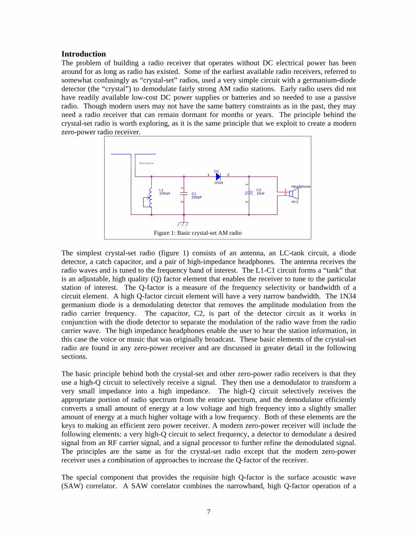
Figure 1: Basic crystal-set AM radio
The simplest crystal-set radio (figure 1) consists of an antenna, an LC-tank circuit, a diode detector, a catch capacitor, and a pair of high-impedance headphones. The antenna receives the radio waves and is tuned to the frequency band of interest. The L1-C1 circuit forms a “tank” that is an adjustable, high quality (Q) factor element that enables the receiver to tune to the particular station of interest. The Q-factor is a measure of the frequency selectivity or bandwidth of a circuit element. A high Q-factor circuit element will have a very narrow bandwidth. The 1N34 germanium diode is a demodulating detector that removes the amplitude modulation from the radio carrier frequency. The capacitor, C2, is part of the detector circuit as it works in conjunction with the diode detector to separate the modulation of the radio wave from the radio carrier wave. The high impedance headphones enable the user to hear the station information, in this case the voice or music that was originally broadcast. These basic elements of the crystal-set radio are found in any zero-power receiver and are discussed in greater detail in the following sections. The basic principle behind both the crystal-set and other zero-power radio receivers is that they use a high-Q circuit to selectively receive a signal. They then use a demodulator to transform a very small impedance into a high impedance. The high-Q circuit selectively receives the appropriate portion of radio spectrum from the entire spectrum, and the demodulator efficiently converts a small amount of energy at a low voltage and high frequency into a slightly smaller amount of energy at a much higher voltage with a low frequency. Both of these elements are the keys to making an efficient zero power receiver. A modern zero-power receiver will include the following elements: a very high-Q circuit to select frequency, a detector to demodulate a desired signal from an RF carrier signal, and a signal processor to further refine the demodulated signal. The principles are the same as for the crystal-set radio except that the modern zero-power receiver uses a combination of approaches to increase the Q-factor of the receiver. The special component that provides the requisite high Q-factor is the surface acoustic wave (SAW) correlator. A SAW correlator combines the narrowband, high Q-factor operation of a
7
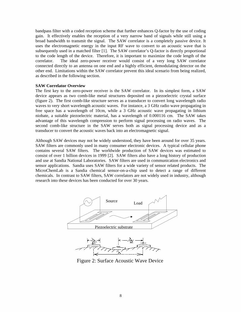
bandpass filter with a coded reception scheme that further enhances Q-factor by the use of coding gain. It effectively enables the reception of a very narrow band of signals while still using a broad bandwidth to transmit the signal. The SAW correlator is a completely passive device. It uses the electromagnetic energy in the input RF wave to convert to an acoustic wave that is subsequently used in a matched filter [1]. The SAW correlator’s Q-factor is directly proportional to the code length of the device. Therefore, it is important to maximize the code length of the correlator. The ideal zero-power receiver would consist of a very long SAW correlator connected directly to an antenna on one end and a highly efficient, demodulating detector on the other end. Limitations within the SAW correlator prevent this ideal scenario from being realized, as described in the following section. SAW Correlator Overview The first key to the zero-power receiver is the SAW correlator. In its simplest form, a SAW
-like metal structures deposited on a piezoelectric crystal surface
for over 35 years. AW filters are commonly used in many consumer electronic devices. A typical cellular phone
device appears as two comb(figure 2). The first comb-like structure serves as a transducer to convert long wavelength radio waves to very short wavelength acoustic waves. For instance, a 3 GHz radio wave propagating in free space has a wavelength of 10cm, while a 3 GHz acoustic wave propagating in lithium niobate, a suitable piezoelectric material, has a wavelength of 0.000116 cm. The SAW takes advantage of this wavelength compression to perform signal processing on radio waves. The second comb-like structure in the SAW serves both as signal processing device and as a transducer to convert the acoustic waves back into an electromagnetic signal. Although SAW devices may not be widely understood, they have been aroundScontains several SAW filters. The worldwide production of SAW devices was estimated to consist of over 1 billion devices in 1999 [2]. SAW filters also have a long history of production and use at Sandia National Laboratories. SAW filters are used in communication electronics and sensor applications. Sandia uses SAW filters for a wide variety of sensor related products. The MicroChemLab is a Sandia chemical sensor-on-a-chip used to detect a range of different chemicals. In contrast to SAW filters, SAW correlators are not widely used in industry, although research into these devices has been conducted for over 30 years.
Piezoelectric substrate
Source Load
Figure 2: Surface Acoustic Wave Device
8
Basic Zero-P
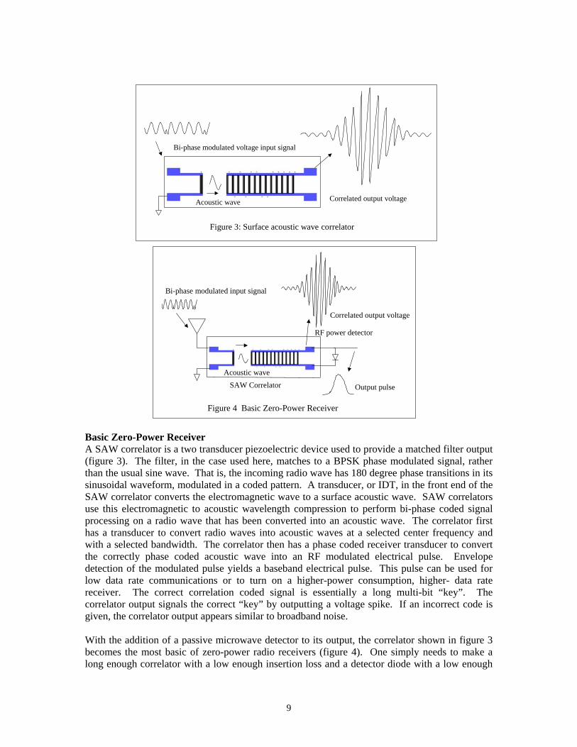
SAW correlator is a two transducer piezoelectric device used to provide a matched filter output ase used here, matches to a BPSK phase modulated signal, rather
, the correlator shown in figure 3 ecomes the most basic of zero-power radio receivers (figure 4). One simply needs to make a
long enough correlator with a low enough insertion loss and a detector diode with a low enough
Bi - phase modulated voltage input signal
Acoustic wave Correlated output voltage
Figure 3: Surface acoustic wave correlator
Bi-phase modulated input signal
Acoustic wave
Correlated output voltage
RF power detector
SAW Correlator Output pulse
Figure 4 Basic Zero-Power Receiver
ower Receiver A(figure 3). The filter, in the cthan the usual sine wave. That is, the incoming radio wave has 180 degree phase transitions in its sinusoidal waveform, modulated in a coded pattern. A transducer, or IDT, in the front end of the SAW correlator converts the electromagnetic wave to a surface acoustic wave. SAW correlators use this electromagnetic to acoustic wavelength compression to perform bi-phase coded signal processing on a radio wave that has been converted into an acoustic wave. The correlator first has a transducer to convert radio waves into acoustic waves at a selected center frequency and with a selected bandwidth. The correlator then has a phase coded receiver transducer to convert the correctly phase coded acoustic wave into an RF modulated electrical pulse. Envelope detection of the modulated pulse yields a baseband electrical pulse. This pulse can be used for low data rate communications or to turn on a higher-power consumption, higher- data rate receiver. The correct correlation coded signal is essentially a long multi-bit “key”. The correlator output signals the correct “key” by outputting a voltage spike. If an incorrect code is given, the correlator output appears similar to broadband noise. With the addition of a passive microwave detector to its outputb
9
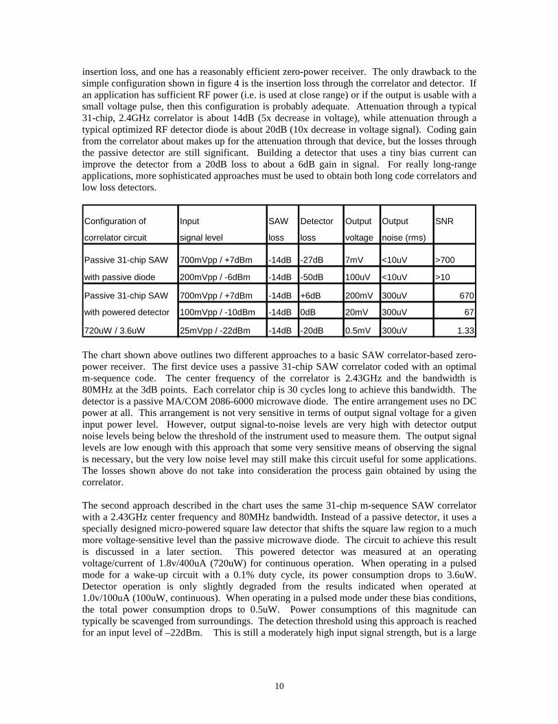
insertion loss, and one has a reasonably efficient zero-power receiver. The only drawback to the simple configuration shown in figure 4 is the insertion loss through the correlator and detector. If an application has sufficient RF power (i.e. is used at close range) or if the output is usable with a small voltage pulse, then this configuration is probably adequate. Attenuation through a typical 31-chip, 2.4GHz correlator is about 14dB (5x decrease in voltage), while attenuation through a typical optimized RF detector diode is about 20dB (10x decrease in voltage signal). Coding gain from the correlator about makes up for the attenuation through that device, but the losses through the passive detector are still significant. Building a detector that uses a tiny bias current can improve the detector from a 20dB loss to about a 6dB gain in signal. For really long-range applications, more sophisticated approaches must be used to obtain both long code correlators and low loss detectors.
Configuration of
The chart shown above outlines two different approaches to a basic SAW correlator-based zero-power receiver. The first device uses a passive 31-chip SAW correlator coded with an optimal m-sequence code. The center frequency of the correlator is 2.43GHz and the bandwidth is
0MHz at the 3dB points. Each correlator chip is 30 cycles long to achieve this bandwidth. The
signed micro-powered square law detector that shifts the square law region to a much ore voltage-sensitive level than the passive microwave diode. The circuit to achieve this result
Input SAW Detector Output Output SNR
correlator circuit signal level loss loss voltage noise (rms)
Passive 31-chip SAW 700mVpp / +7dBm -14dB -27dB 7mV <10uV >700
with passive diode 200mVpp / -6dBm -14dB -50dB 100uV <10uV >10
Passive 31-chip SAW 700mVpp / +7dBm -14dB +6dB 200mV 300uV 670
with powered detector 100mVpp / -10dBm -14dB 0dB 20mV 300uV 67
720uW / 3.6uW 25mVpp / -22dBm -14dB -20dB 0.5mV 300uV 1.33
8detector is a passive MA/COM 2086-6000 microwave diode. The entire arrangement uses no DC power at all. This arrangement is not very sensitive in terms of output signal voltage for a given input power level. However, output signal-to-noise levels are very high with detector output noise levels being below the threshold of the instrument used to measure them. The output signal levels are low enough with this approach that some very sensitive means of observing the signal is necessary, but the very low noise level may still make this circuit useful for some applications. The losses shown above do not take into consideration the process gain obtained by using the correlator. The second approach described in the chart uses the same 31-chip m-sequence SAW correlator with a 2.43GHz center frequency and 80MHz bandwidth. Instead of a passive detector, it uses a specially demis discussed in a later section. This powered detector was measured at an operating voltage/current of 1.8v/400uA (720uW) for continuous operation. When operating in a pulsed mode for a wake-up circuit with a 0.1% duty cycle, its power consumption drops to 3.6uW. Detector operation is only slightly degraded from the results indicated when operated at 1.0v/100uA (100uW, continuous). When operating in a pulsed mode under these bias conditions, the total power consumption drops to 0.5uW. Power consumptions of this magnitude can typically be scavenged from surroundings. The detection threshold using this approach is reached for an input level of –22dBm. This is still a moderately high input signal strength, but is a large
10
improvement in sensitivity over the entirely passive approach. The detector circuit dominates the noise output of this approach. The correlators used in this work make use solely of BPSK signals. The correlator can provide considerable process gain by converting the input BPSK signal with a matched pattern into an RF
nd frequency. The baseband envelope pulse is
er converts acoustic energy electrical energy, typically being electrically terminated in some low impedance such as 50Ω
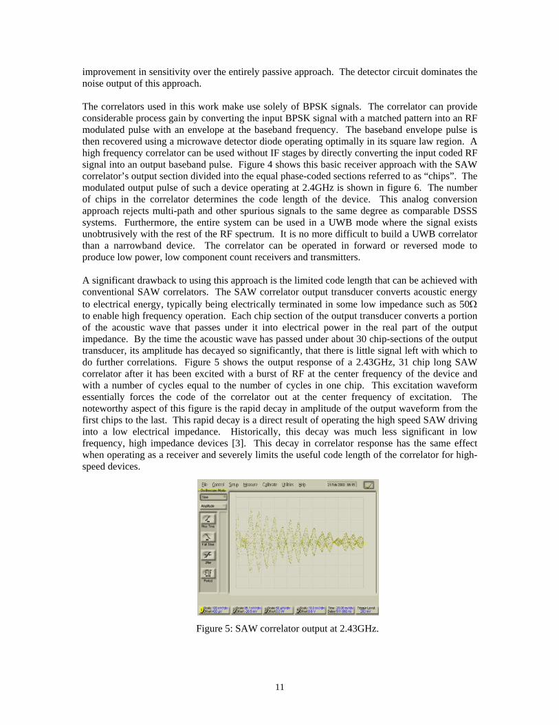
modulated pulse with an envelope at the basebathen recovered using a microwave detector diode operating optimally in its square law region. A high frequency correlator can be used without IF stages by directly converting the input coded RF signal into an output baseband pulse. Figure 4 shows this basic receiver approach with the SAW correlator’s output section divided into the equal phase-coded sections referred to as “chips”. The modulated output pulse of such a device operating at 2.4GHz is shown in figure 6. The number of chips in the correlator determines the code length of the device. This analog conversion approach rejects multi-path and other spurious signals to the same degree as comparable DSSS systems. Furthermore, the entire system can be used in a UWB mode where the signal exists unobtrusively with the rest of the RF spectrum. It is no more difficult to build a UWB correlator than a narrowband device. The correlator can be operated in forward or reversed mode to produce low power, low component count receivers and transmitters. A significant drawback to using this approach is the limited code length that can be achieved with conventional SAW correlators. The SAW correlator output transductoto enable high frequency operation. Each chip section of the output transducer converts a portion of the acoustic wave that passes under it into electrical power in the real part of the output impedance. By the time the acoustic wave has passed under about 30 chip-sections of the output transducer, its amplitude has decayed so significantly, that there is little signal left with which to do further correlations. Figure 5 shows the output response of a 2.43GHz, 31 chip long SAW correlator after it has been excited with a burst of RF at the center frequency of the device and with a number of cycles equal to the number of cycles in one chip. This excitation waveform essentially forces the code of the correlator out at the center frequency of excitation. The noteworthy aspect of this figure is the rapid decay in amplitude of the output waveform from the first chips to the last. This rapid decay is a direct result of operating the high speed SAW driving into a low electrical impedance. Historically, this decay was much less significant in low frequency, high impedance devices [3]. This decay in correlator response has the same effect when operating as a receiver and severely limits the useful code length of the correlator for high-speed devices.
Figure 5: SAW correlator output at 2.43GHz.
11
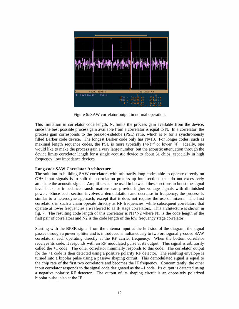
Figure 6: SAW correlator output in normal operation.
his limitation in correlator code length, N, limits the process gain available from the device,
ong-code SAW Correlator Architecture ith arbitrarily long codes able to operate directly on
tarting with the BPSK signal from the antenna input at the left side of the diagram, the signal
bipolar pulse, also at the IF.
Tsince the best possible process gain available from a correlator is equal to N. In a correlator, the process gain corresponds to the peak-to-sidelobe (PSL) ratio, which is N for a synchronously filled Barker code device. The longest Barker code only has N=13. For longer codes, such as maximal length sequence codes, the PSL is more typically (4N)1/2 or lower [4]. Ideally, one would like to make the process gain a very large number, but the acoustic attenuation through the device limits correlator length for a single acoustic device to about 31 chips, especially in high frequency, low impedance devices. LThe solution to building SAW correlators wGHz input signals is to split the correlation process up into sections that do not excessively attenuate the acoustic signal. Amplifiers can be used in between these sections to boost the signal level back, or impedance transformations can provide higher voltage signals with diminished power. Since each section involves a demodulation and decrease in frequency, the process is similar to a heterodyne approach, except that it does not require the use of mixers. The first correlators in such a chain operate directly at RF frequencies, while subsequent correlators that operate at lower frequencies are referred to as IF stage correlators. This architecture is shown in fig. 7. The resulting code length of this correlator is N1*N2 where N1 is the code length of the first pair of correlators and N2 is the code length of the low frequency stage correlator. Spasses through a power splitter and is introduced simultaneously to two orthogonally-coded SAW correlators, each operating directly at the RF carrier frequency. When the bottom correlator receives its code, it responds with an RF modulated pulse at its output. This signal is arbitrarily called the +1 code. The other correlator minimally responds to this code. The correlator output for the +1 code is then detected using a positive polarity RF detector. The resulting envelope is turned into a bipolar pulse using a passive shaping circuit. This demodulated signal is equal to the chip rate of the first two correlators and becomes the IF frequency. Concomitantly, the other input correlator responds to the signal code designated as the –1 code. Its output is detected using a negative polarity RF detector. The output of its shaping circuit is an oppositely polarized
12
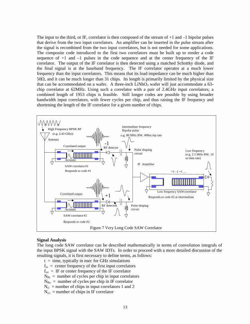
The input to the third, or IF, correlator is then composed of the stream of +1 and –1 bipolar pulses
at derive from the two input correlators. An amplifier can be inserted in the pulse stream after
he long code SAW correlator can be described mathematically in terms of convolution integrals of ignal with the SAW IDTs. In order to proceed with a more detailed discussion of the
s
ththe signal is recombined from the two input correlators, but is not needed for some applications. The composite code introduced to the first two correlators must be built up to render a code sequence of +1 and –1 pulses in the code sequence and at the center frequency of the IF correlator. The output of the IF correlator is then detected using a matched Schottky diode, and the final signal is at the baseband frequency. The IF correlator operates at a much lower frequency than the input correlators. This means that its load impedance can be much higher than 50Ω, and it can be much longer than 31 chips. Its length is primarily limited by the physical size that can be accommodated on a wafer. A three-inch LiNbO3 wafer will just accommodate a 63-chip correlator at 62MHz. Using such a correlator with a pair of 2.4GHz input correlators; a combined length of 1953 chips is feasible. Still longer codes are possible by using broader bandwidth input correlators, with fewer cycles per chip, and thus raising the IF frequency and shortening the length of the IF correlator for a given number of chips.
Signal Analysis Tthe input BPSK sresulting signals, it is first necessary to define terms, as follows:
t = time, typically in nsec for GHz simulations foi = center frequency of the first input correlators foo = IF or center frequency of the IF correlator NBi = number of cycles per chip in input correlatorNBo = number of cycles per chip in IF correlatorNci = number of chips in input correlators 1 and 2 Nco = number of chips in IF correlator
Acoustic
Correlated output l
SAW correlator #2
Acoustic
SAW correlator #1
High Frequency BPSK RF i
Antenna
Responds to code #1
Responds to code #2
+1
- 1
Correlated output
(e.g. 2.43 GHz))
Intermediate frequencyBipolar pulse
(e.g. 80 MHz BW, 400ns rep rate )
l
IF Amplifier
Low frequency SAW correlator Responds to code #3 at intermediate f
Figure 7 Very Long Code SAW Correlator
Low frequency (e.g. 2.5 MHz BW, 10 us data rate)
+1 – 1 +1 …
RF detector
RF detector
Pulse shapingcircuit
Pulse shapingcircuit
13
Tci = NBi / foi = chip time of input correlators Tco = NBo / foo = chip time of IF correlator
rs r
mbly r. 1
The t response from the first of the input correlators can be described as a stream of sine waves with varying phases as seen in
The BPSK input sign gonal to the code of the first
put correlator. The input BPSK signal to obtain a correlation output pulse from this correlator is
Here ax1 and ax2 orthogonal. Both of these input signals
y the chip sequence
The electrical input signals v to be converted into coustic waves. This input transducer typically consists of NBi finger-pairs of metal spaced at the
and typically pi1(t) = pi2 scribe a windowing function. The peration of electrically exciting this transducer with the input wave vi1(t) or vi2(t) is represented by a me domain convolution operation, so that the output acoustic wave is given by
TBi = NBi Nci / foi = bit time of input correlatoTBo = NBo Nco / foo = bit time of IF correlatofci = 1 / Tci = chip rate of input correlators fco = 1 / Tco = chip rate of IF correlator fDi = 1 / TBi = data rate of input correlators fDo = 1 / TBo = data rate of complete asseax1 = 1,-1,-1,1,1,… = BPSK input code, corax2 = -1,-1,1,1,-1,… = orthogonal code, corr. 2 bx1 = 1,1,-1,-1,1,… = time reversed input1 code bx2 = -1,1,1,-1,-1,… = time reversed input2 codecjo = 0,0,1,1,1,… = IF correlator input code djo = 1,1,1,0,0,… = time reversed IF corr. code u(t) = 0 if (t < 0), else 1 = unit step function input BPSK signal (figure 8) to obtain a correc
al to the second of the input correlators uses a code that is orthoin
are the coefficient vectors that are mutuallyconsist of a sine wave at the center frequency of the input correlator modulated bof the input codes. Each will excite a single correlation pulse output from one of the input correlators. The correlator output transducer serves as a matched filter to the input BPSK signal. The impulse response of the transducer for the first correlator is
i1(t) and vi2(t) must pass through input transducers acenter frequency of the correlator. The impulse response of this type of input transducer for the first correlator is given by
(t). These input transducers each de
oti
v i2 t( ) sin 2π f oi⋅ t⋅( )N ci
a x2 u t x 1−( ) T ci⋅−
v i1 t( ) sin 2π f oi⋅ t⋅( )1x
a x1 u t x 1−( ) T ci⋅−
N ci⋅∑
=
⋅:= u t xT ci⋅−( )−⎡ ⎡ ⎤ ⎤⎣ ⎣ ⎦ ⎦
1x
⎡⎣ ⎤⎦ u t xT ci⋅−( )−⎡⎣ ⎤⎦⋅∑⋅:=
=
c t( ) sin 2 π⋅ f⋅ t⋅( )N ci
b u ti1 oi1x
x1 x 1−( ) Tci⋅− u t xT ci⋅−( )−⎡ ⎡ ⎤ ⎤⎣ ⎣ ⎦ ⎦⋅∑⋅:=
=
pi1 t( ) sin 2 π⋅ foi⋅ t⋅( ) u t( ) u t Tci−( )−( )⋅:=
14
The acoustic wave represented by distortion due to the band limiting action of the input transducer. The wav with the output transducer impulse
sponse to produce the final electrical output y (t) of the SAW correlator. The electrical output of
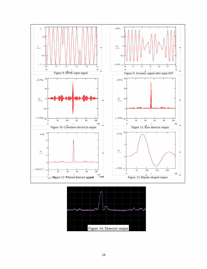
This resulting output sign odulating a sinusoidal center frequency signal. Simulation results for a 31-chip input c the 2.4GHz center frequency are shown in figure 0. This analysis includes the effect of the correlator input transducer, which causes some distortion
. The correct input waveform to the complete correlator assembly is then a coded tream of the v (t) and v (t) signals. Each of these output pulses is first envelope detected by a
with k1 and k2 being cons plitude. This raw detector output (figure 11) is typically not e output is further filtered by a combination of
arasitic and added capacitance at the output of the detector. This filtered output signal (figure 12) is
The time-constant, τo, of this out mined by the detector video resistance Rv and the output capacitance Cv.
e the input transducer of the IF correlator. Another passive circuit, a two-pole ifferentiator-shaping filter, easily performs this conversion process. This circuit consists of a damped
ac 1 t( )t
0
τv i1 τ( ) p i1 t τ−( )⋅⌠⎮ d:=⌡
ac1(t) (figure 9) shows some e, ac1(t), is then convolved
re i1this convolution operation is given by
y o1 t( )t
τ
0
c i1 τ ac 1 t τ−⋅⎮⌡
d:= ( ) ( )⌠
al is a correlation pulse morrelator at
1to the acoustic wave (fig. 9) and, as a result, also to the output waveform (fig. 10). The second input correlator produces a corresponding yo2(t) output signal by a similar convolution when excited by the vi2(t) input signal. Each of these output pulses represented by yo1(t) and yo2(t) must be converted into a single cycle input to the IF correlators i1 i2microwave diode detector. This device typically operates in some combination of linear and square-law operation, depending on the strength of the input signal. The detector output is given as
yoD t( ) k1 yo1 t( )( )2⋅ k2 yo1 t( )⋅+:=
tants that vary with the input signal am an observed signal, as th
pgiven by
put filter is deter
The output yoF(t) of the diode detector is a unipolar pulse. This must be converted into a bipolar pulse to most effectively drivdLC high-pass filter with a time constant well below the input pulse bandwidth. The operation of the filtered detector output passing through this filter (fig. 13) is yet another convolution and is given by
yoF t( )0
τyoD τ( ) eτo
tt τ−( )−
⋅⎮⎮⌡
d:= yoD
⌠⎮
15
This output signal, yoB(t), represents only one bipolar pulse in a train of pulses that make up the
put to the IF correlator. The input signals applied to the two input correlators must consist of a coded
This comp chips long. It is the signal that gets transmitted to the receiver and comes in at the antenna. The resulting output signal combined from the two input
in set of shorter length codes, vi1(t) and vi2(t). The coding applied to the stream of vi1(t) and vi2(t)
signals is itself the code, cjo, of the IF correlator. The complete input waveform to generate the combined signal is
lete BPSK input signal is NciNco
correlators is the sum of the two final signals, yoaB(t) and yobB(t), where the subscript ‘a’ represents the ‘1’ correlator and the subscript ‘b’ represents the ‘-1’ correlator. Both of these signals are approximately of the form
B
This is just a single cy the IF correlator. The input to the
correlator is then a coded stream of these signals as represented by
This input si correlator by the input
ansducer. This input transducer to the IF correlator has an impulse response given by
This is similar in form t the input frequency, foo, and the hip width, Tco, of the IF correlator are markedly different from that of the input correlators. The
which is the time-domain convol t signal with the wideband transducer impulse
sponse. This signal is similar in appearance to that shown in figure 9. This acoustic signal must
t
yoB t( )
0
τyoF τ( ) sint τ−
τo2
⎛⎜⎝
⎞⎟⎠
⋅ e
t τ−( )−
τo3⋅
⌠⎮⎮⎮⎮⌡
d:= yoF
v i t( )
1j
c jo v i1 t( )⋅ 1 c jo−( ) v i2 t( )⋅+
N co
∑=
:= ⎡
cle of a sine wave at the center frequency of IF
gnal is then transformed into an acoustic signal in the IFtr
to the impulse response given by pi1(t) , bu
cacoustic signal in the IF correlator is then given by
ution of the inpurethen match the output transducer’s finger pattern given by
⎣ ⎤⎦
y oa4 t( ) sin 2 π⋅ f oo⋅ t⋅( ) u t( ) u tf oo
−⎛ ⎛ 1−⎜
⎝⎞⎟⎠
⎜⎝
⎞⋅:= ⎟⎠
v iIF t( )
N coc jo y oa4 t j T co⋅−( )⋅ 1 c jo−( ) y ob4 t −(⋅+
1j
j T co⋅ )⎡⎣ ⎤⎦∑:=
=
p iIF t( ) sin 2 π⋅ f oo⋅ t⋅( ) u t( ) u t T co−( )−( )⋅:=
ac IF t( )t
0
τv iIF τ( ) ( )⌠⎮⌡
:= p iIF t τ−⋅ d
c oIF t( ) sin 2 π⋅ f oo⋅ t⋅( )N co 1−
d jo u t j T co⋅−(0j
) u t j 1+( ) T co⋅−⎡⎣ ⎤⎦−⎡⎣ ⎤⎦⋅∑⋅:=
=
16
The acoustic signal will be convolved with this output transducer pattern, producing an electrical signal, as given by
yoIF t( )0
tτcoIF τ( ) acIF t τ−( )⋅
⌠⎮⌡
d:=
This signal passes through a detector diode, which has different optimization parameters from the input detector diodes. This detected signal is given by
y oIF2 t( ) k 3 y oIF t( )( )2⋅ k 4 y oIF t( )⋅+:=
Where k3 and k4 are square-law and linear region constants determined by the magnitude of the input signal yoIF(t). This raw detector output is filtered by the output capacitance of the detector circuit. This filtering process is given by
y oIF3 t( )0
t
τy oIF2 τ( ) e
t τ−( )−
τ oIF⋅
⌠⎮⎮⎮⌡
d:=
For optimum response, the time constant τoIF is needs to be much longer than the time constant, τo, applied to the input detectors. This is because the output data time, fDo, to which the detector time constant should be matched, is much longer than the data time of the input correlators given by fDi. This implies that the output impedance that the final detector sees can be made higher than the output impedance of the IF correlator. This provides an opportunity to increase the output signal voltage, even though power has been lost through the correlation process. This final output signal, yoIF3(t), is the output of the entire combined correlator. It is similar in shape to fig. 12 with a time constant determined by the output data time, fDo. Figures 8-13 are simulated output results obtained by applying the analysis just provided with actual component values inserted for the various constants. Experimental Results of Long SAW Approach A complete long SAW correlator was built using this methodology. The two input correlators operate at 2.43GHz center frequency and have orthogonal codes 31 chips long. Each chip contains 30 cycles, giving the correlator a 3.3% input bandwidth. The detector diodes are matched to about 100Ω at their input and matched to about 400Ω at their output. This is roughly an optimum match to the input SAW device, and the increase in impedance through the detector allows for an increase in signal voltage. The use of passive detectors causes significant attenuation through the entire chain. The pulse bandwidth out of the diode detectors is 80 MHz. A signal out of one of the detectors is shown in figure 14. The central peak is the correlation peak and indicates the correct detection of a signal. The sidelobes occur from minor correlations and defects in the correlation process and constitute noise through the remainder of the circuit. The pulse shaping circuit is a two-pole differentiator with a self-resonant frequency of 8MHz. The differentiator is just a two pole LC circuit configured as a high pass filter with its corner frequency somewhat below the frequency of the input unipolar pulse. This circuit turns the unipolar pulses into bipolar pulses with a center frequency of 62MHz. A signal out of one of the shaping circuits is shown in figure 15. Because the signal is a single cycle of a sinusoid, it has a very wide bandwidth.
17
10 11 12 13 14 151
0.5
0
0.5
11
1−
v
1510 t10 11 12 13 14 15 16
1
0.5
0
0.5
10.833
0.833−
acc
1610 t
0 20 40 60 80 10010
0
10
20
3026.52
0.025−
y2
1050 t
0 20 40 60 80 1002
0
2
4
6
86.28
1.019− 10 3−×
y3
1050 tτo2 20:= τo3 80:= nsec
0 50 100 150 2005
0
5
109.116
3.963−
y4
2400 t
Figure 8: BPSK input signal Figure 9: Acoustic signal after input IDT
Figure 10: Correlator electrical output Figure 11: Raw detector output
Figure 12: Filtered detector output Figure 13: Bipolar shaped output
0 20 40 60 80 10020
10
0
10
2015.793
15.783−
y1
1050 t
Figure 14: Detector output
18
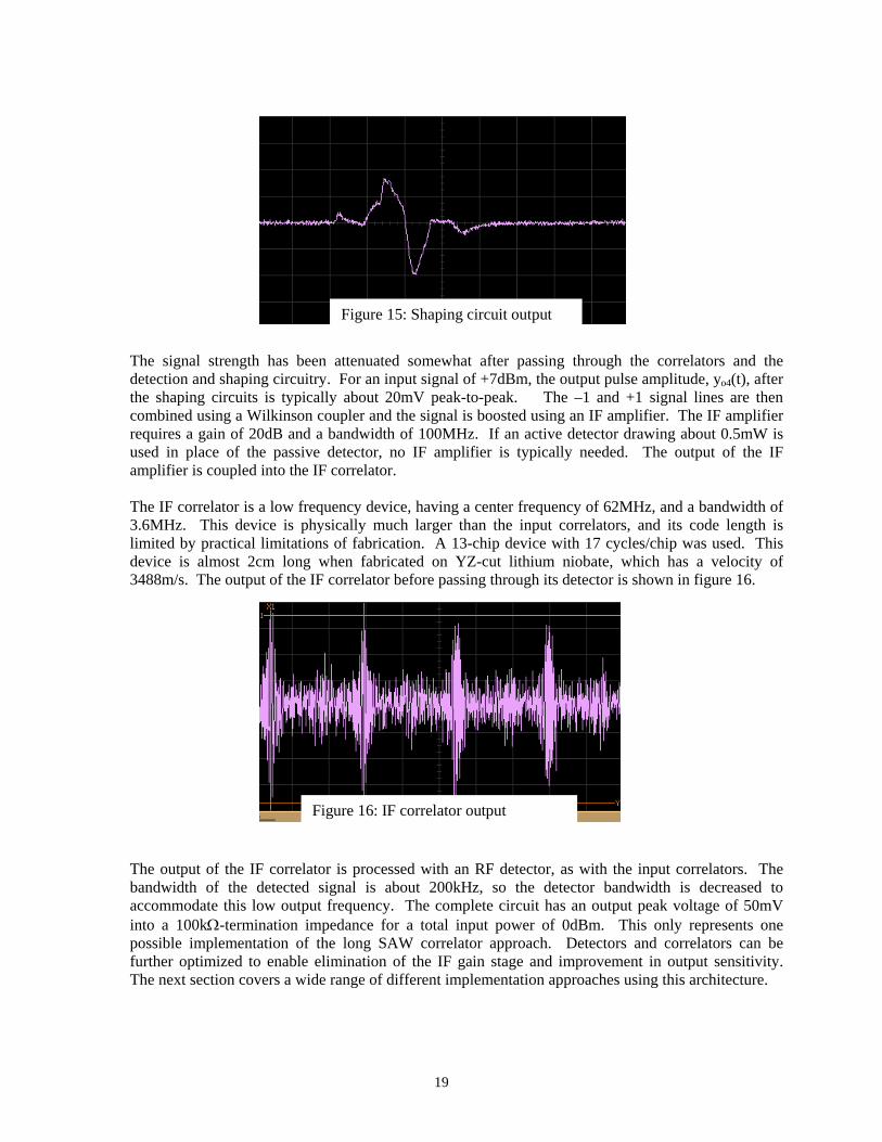
Figure 15: Shaping circuit output
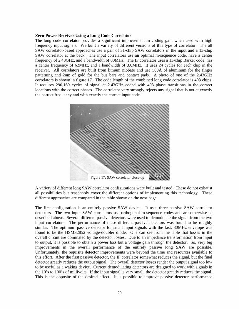
The signal strength has been attenuated somewhat after passing through the correlators and the detection and shaping circuitry. For an input signal of +7dBm, the output pulse amplitude, yo4(t), after the shaping circuits is typically about 20mV peak-to-peak. The –1 and +1 signal lines are then combined using a Wilkinson coupler and the signal is boosted using an IF amplifier. The IF amplifier requires a gain of 20dB and a bandwidth of 100MHz. If an active detector drawing about 0.5mW is used in place of the passive detector, no IF amplifier is typically needed. The output of the IF amplifier is coupled into the IF correlator. The IF correlator is a low frequency device, having a center frequency of 62MHz, and a bandwidth of 3.6MHz. This device is physically much larger than the input correlators, and its code length is limited by practical limitations of fabrication. A 13-chip device with 17 cycles/chip was used. This device is almost 2cm long when fabricated on YZ-cut lithium niobate, which has a velocity of 3488m/s. The output of the IF correlator before passing through its detector is shown in figure 16.
Figure 16: IF correlator output The output of the IF correlator is processed with an RF detector, as with the input correlators. The bandwidth of the detected signal is about 200kHz, so the detector bandwidth is decreased to accommodate this low output frequency. The complete circuit has an output peak voltage of 50mV into a 100kΩ-termination impedance for a total input power of 0dBm. This only represents one possible implementation of the long SAW correlator approach. Detectors and correlators can be further optimized to enable elimination of the IF gain stage and improvement in output sensitivity. The next section covers a wide range of different implementation approaches using this architecture.
19
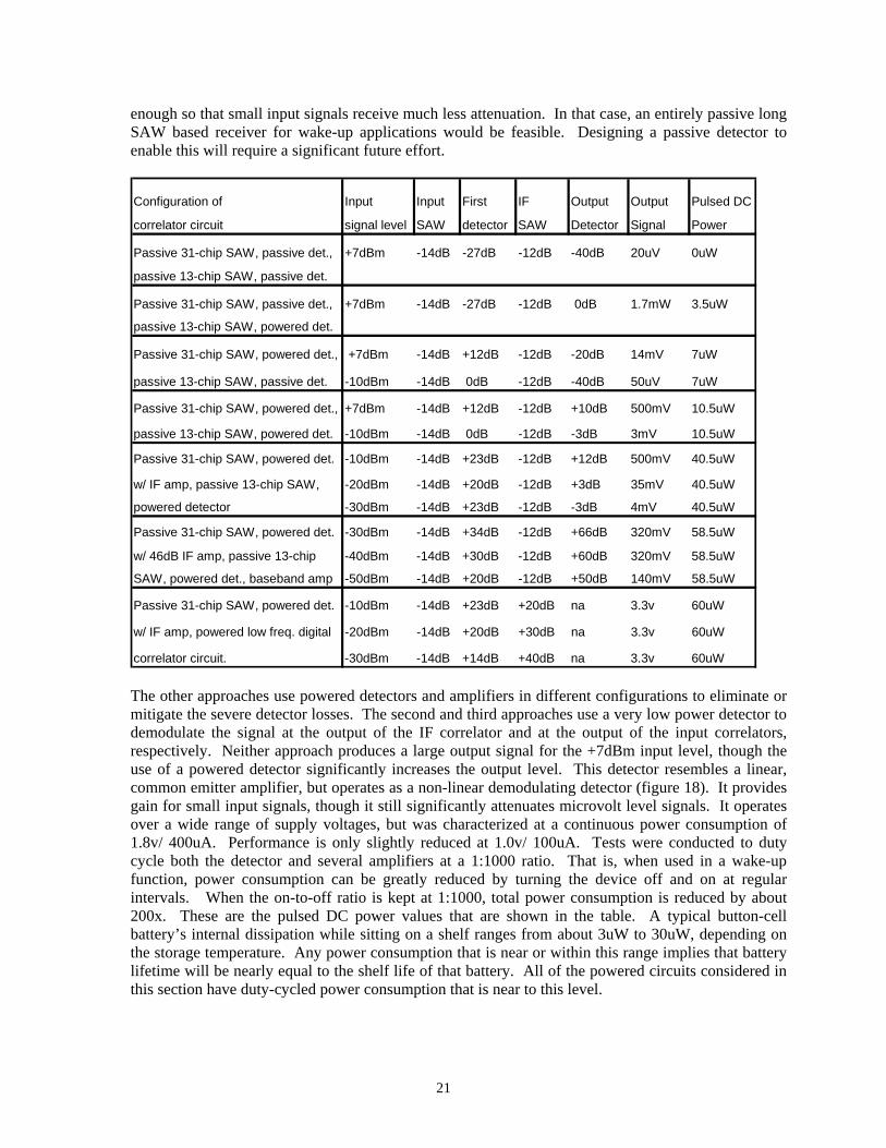
Zero-Power Receiver Using a Long Code Correlator The long code correlator provides a significant improvement in coding gain when used with high frequency input signals. We built a variety of different versions of this type of correlator. The all SAW correlator-based approaches use a pair of 31-chip SAW correlators in the input and a 13-chip SAW correlator at the back. The input correlators use an optimal m-sequence code, have a center frequency of 2.43GHz, and a bandwidth of 80MHz. The IF correlator uses a 13-chip Barker code, has a center frequency of 62MHz, and a bandwidth of 3.6MHz. It uses 24 cycles for each chip in the receiver. All correlators are built from lithium niobate and use 500Å of aluminum for the finger patterning and 2um of gold for the bus bars and contact pads. A photo of one of the 2.43GHz correlators is shown in figure 17. The code length of the combined long code correlator is 403 chips. It requires 290,160 cycles of signal at 2.43GHz coded with 403 phase transitions in the correct locations with the correct phases. The correlator very strongly rejects any signal that is not at exactly the correct frequency and with exactly the correct input code.
Figure 17: SAW correlator close-up A variety of different long SAW correlator configurations were built and tested. These do not exhaust all possibilities but reasonably cover the different options of implementing this technology. These different approaches are compared in the table shown on the next page. The first configuration is an entirely passive SAW device. It uses three passive SAW correlator detectors. The two input SAW correlators use orthogonal m-sequence codes and are otherwise as described above. Several different passive detectors were used to demodulate the signal from the two input correlators. The performance of these different passive detectors was found to be roughly similar. The optimum passive detector for small input signals with the fast, 80MHz envelope was found to be the HSMS2852 voltage-doubler diode. One can see from the table that losses in the overall circuit are dominated by the detector losses. Due to an impedance transformation from input to output, it is possible to obtain a power loss but a voltage gain through the detector. So, very big improvements in the overall performance of the entirely passive long SAW are possible. Unfortunately, the requisite detector improvements were beyond the time and resources available to this effort. After the first passive detector, the IF correlator somewhat reduces the signal, but the final detector greatly reduces the output signal. The overall detector losses render the output signal too low to be useful as a waking device. Current demodulating detectors are designed to work with signals in the 10’s to 100’s of millivolts. If the input signal is very small, the detector greatly reduces the signal. This is the opposite of the desired effect. It is possible to improve passive detector performance
20
enough so that small input signals receive much less attenuation. In that case, an entirely passive long SAW based receiver for wake-up applications would be feasible. Designing a passive detector to enable this will require a significant future effort.
he other approaches use powered detectors and amplifiers in different configurations to eliminate or
Configuration of Input Input First IF Output Output Pulsed DC
correlator circuit signal level SAW detector SAW Detector Signal Power
Passive 31-chip SAW, passive det., +7dBm -14dB -27dB -12dB -40dB 20uV 0uW
passive 13-chip SAW, passive det.
Passive 31-chip SAW, passive det., +7dBm -14dB -27dB -12dB 0dB 1.7mW 3.5uW
passive 13-chip SAW, powered det.
Passive 31-chip SAW, powered det., +7dBm -14dB +12dB -12dB -20dB 14mV 7uW
passive 13-chip SAW, passive det. -10dBm -14dB 0dB -12dB -40dB 50uV 7uW
Passive 31-chip SAW, powered det., +7dBm -14dB +12dB -12dB +10dB 500mV 10.5uW
passive 13-chip SAW, powered det. -10dBm -14dB 0dB -12dB -3dB 3mV 10.5uW
Passive 31-chip SAW, powered det. -10dBm -14dB +23dB -12dB +12dB 500mV 40.5uW
w/ IF amp, passive 13-chip SAW, -20dBm -14dB +20dB -12dB +3dB 35mV 40.5uW
powered detector -30dBm -14dB +23dB -12dB -3dB 4mV 40.5uW
Passive 31-chip SAW, powered det. -30dBm -14dB +34dB -12dB +66dB 320mV 58.5uW
w/ 46dB IF amp, passive 13-chip -40dBm -14dB +30dB -12dB +60dB 320mV 58.5uW
SAW, powered det., baseband amp -50dBm -14dB +20dB -12dB +50dB 140mV 58.5uW
Passive 31-chip SAW, powered det. -10dBm -14dB +23dB +20dB na 3.3v 60uW
w/ IF amp, powered low freq. digital -20dBm -14dB +20dB +30dB na 3.3v 60uW
correlator circuit. -30dBm -14dB +14dB +40dB na 3.3v 60uW Tmitigate the severe detector losses. The second and third approaches use a very low power detector to demodulate the signal at the output of the IF correlator and at the output of the input correlators, respectively. Neither approach produces a large output signal for the +7dBm input level, though the use of a powered detector significantly increases the output level. This detector resembles a linear, common emitter amplifier, but operates as a non-linear demodulating detector (figure 18). It provides gain for small input signals, though it still significantly attenuates microvolt level signals. It operates over a wide range of supply voltages, but was characterized at a continuous power consumption of 1.8v/ 400uA. Performance is only slightly reduced at 1.0v/ 100uA. Tests were conducted to duty cycle both the detector and several amplifiers at a 1:1000 ratio. That is, when used in a wake-up function, power consumption can be greatly reduced by turning the device off and on at regular intervals. When the on-to-off ratio is kept at 1:1000, total power consumption is reduced by about 200x. These are the pulsed DC power values that are shown in the table. A typical button-cell battery’s internal dissipation while sitting on a shelf ranges from about 3uW to 30uW, depending on the storage temperature. Any power consumption that is near or within this range implies that battery lifetime will be nearly equal to the shelf life of that battery. All of the powered circuits considered in this section have duty-cycled power consumption that is near to this level.
21
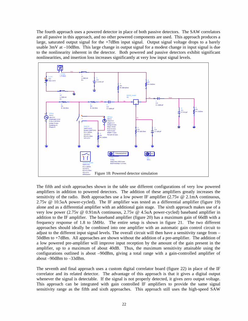
The fourth approach uses a powered detector in place of both passive detectors. The SAW correlators are all passive in this approach, and no other powered components are used. This approach produces a large, saturated output signal for the +7dBm input signal. Output signal voltage drops to a barely usable 3mV at –10dBm. This large change in output signal for a modest change in input signal is due to the nonlinearity inherent in the detector. Both powered and passive detectors exhibit significant nonlinearities, and insertion loss increases significantly at very low input signal levels.
Vout
Vb
Vc
Ve
Vin
Vcc
V_DCVccVdc=1.8 V
VtSineVsrc1
Phase=0Damping=0Delay=0 nsecFreq=2.43 GHzAmplitude=4 mVVdc=0 V
CC1C=5.0 pF
RR7R=3 kOhmR
R5R=300 kOhm
TranTran1
MaxTimeStep=1.0 nsecStopTime=100.0 nsec
TRANSIENT
CC5C=0.01 uF
LL2
R=L=500 nH
LL1
R=L=500 nH
I_ProbeI_Probe1
RR6R=2 kOhm
VtPulseSRC2
Period=15 nsecWidth=7 nsecFall=5 nsecRise=5 nsecEdge=linearDelay=0 nsecVhigh=1 VVlow=0 V
t
CC4C=100 pF
RR3R=100 Ohm
CC3C=1000 pF
SwitchV_ModelSWITCH1
AllParams=V2=1.0 VR2=0.1 OhmV1=0.0 VR1=1 kOhm
V
DCDC1
DC
CC2C=1000 pF
RR2R=50 Ohm
bfu510_modelX1
SwitchVSWITCHV1
V2=1.0 VR2=0.1 OhmV1=0.0 VR1=1 kOhmModel=SWITCH1
V
RR4R=1 kOhm
RR1R=50 Ohm
Figure 18: Powered detector simulation
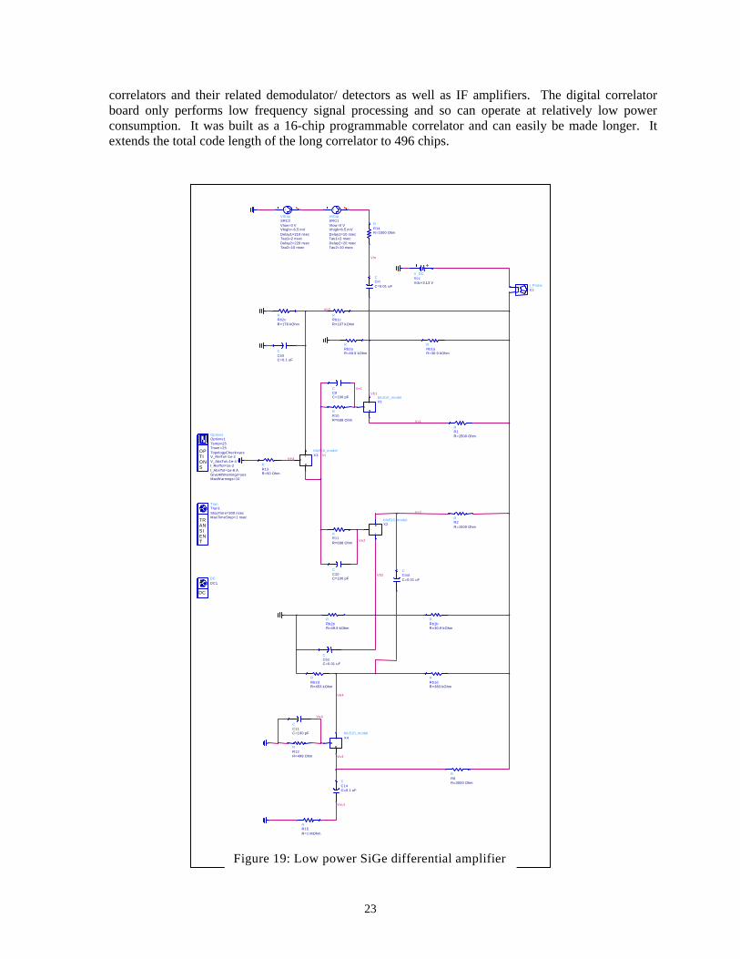
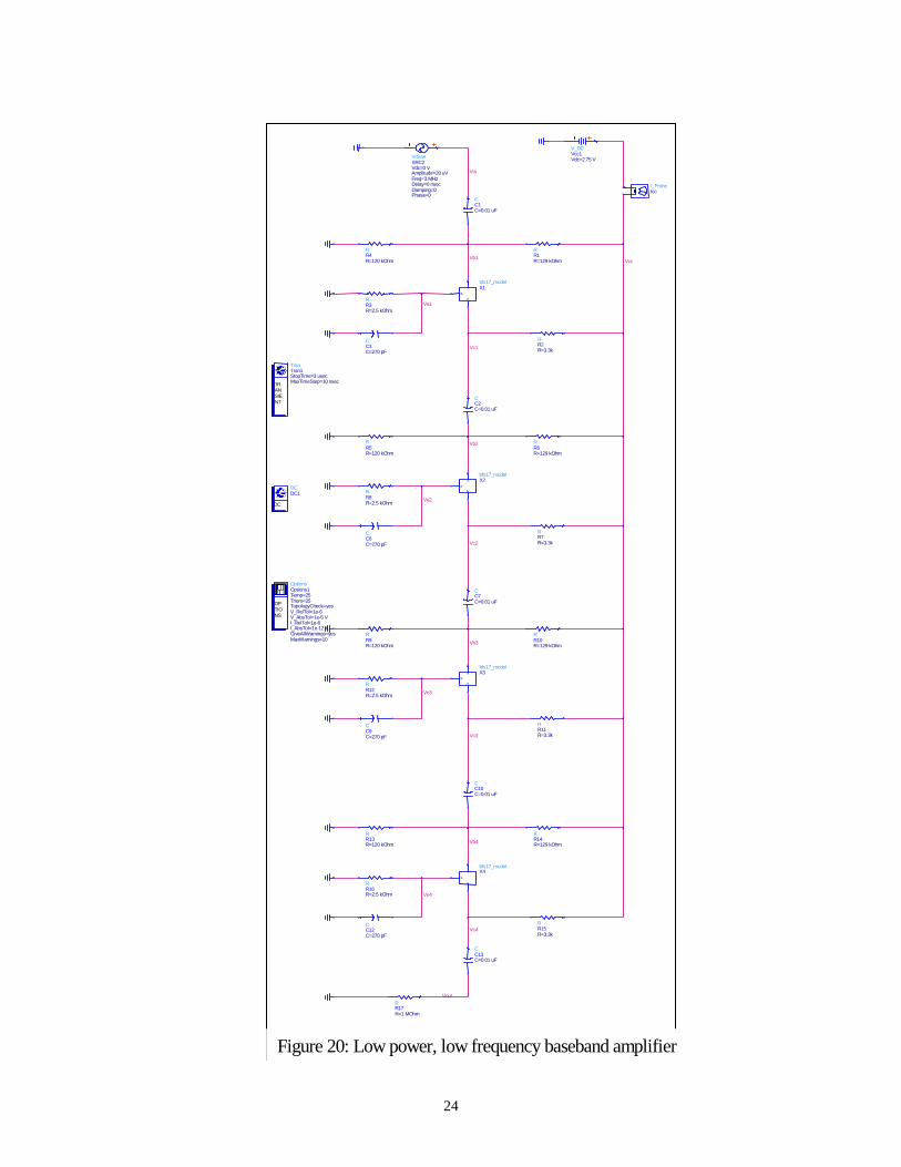
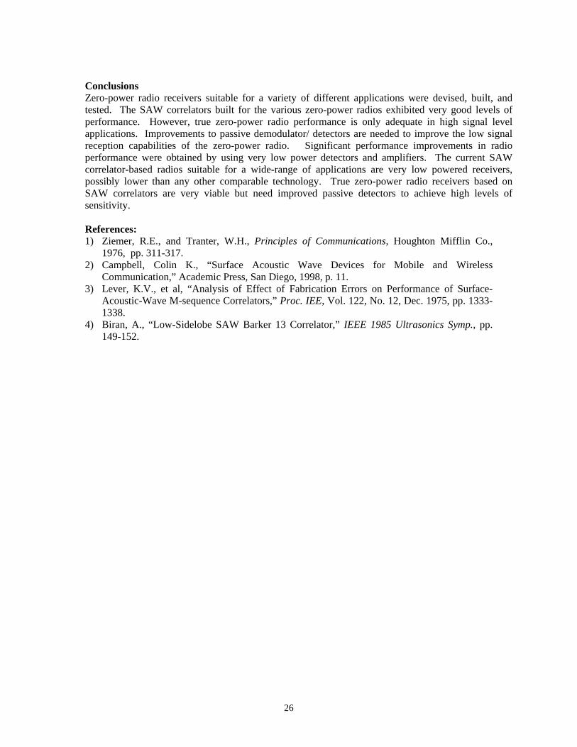
The fifth and sixth approaches shown in the table use different configurations of very low powered amplifiers in addition to powered detectors. The addition of these amplifiers greatly increases the sensitivity of the radio. Both approaches use a low power IF amplifier (2.75v @ 2.1mA continuous, 2.75v @ 10.5uA power-cycled). The IF amplifier was tested as a differential amplifier (figure 19) alone and as a differential amplifier with an additional gain stage. The sixth approach makes use of a very low power (2.75v @ 0.91mA continuous, 2.75v @ 4.5uA power-cycled) baseband amplifier in addition to the IF amplifier. The baseband amplifier (figure 20) has a maximum gain of 66dB with a frequency response of 1.8 to 5MHz. The entire setup is shown in figure 21. The two different approaches should ideally be combined into one amplifier with an automatic gain control circuit to adjust to the different input signal levels. The overall circuit will then have a sensitivity range from –50dBm to +7dBm. All approaches are shown without the addition of a pre-amplifier. The addition of a low powered pre-amplifier will improve input reception by the amount of the gain present in the amplifier, up to a maximum of about 40dB. Thus, the maximum sensitivity attainable using the configurations outlined is about –90dBm, giving a total range with a gain-controlled amplifier of about –90dBm to –33dBm. The seventh and final approach uses a custom digital correlator board (figure 22) in place of the IF correlator and its related detector. The advantage of this approach is that it gives a digital output whenever the signal is detectable. If the signal is not properly detected, it gives zero output voltage. This approach can be integrated with gain controlled IF amplifiers to provide the same signal sensitivity range as the fifth and sixth approaches. This approach still uses the high-speed SAW
22
correlators and their related demodulator/ detectors as well as IF amplifiers. The digital correlator board only performs low frequency signal processing and so can operate at relatively low power consumption. It was built as a 16-chip programmable correlator and can easily be made longer. It extends the total code length of the long correlator to 496 chips.
Vout
Vc4
Ve4
Vb4
Vb2
Vc2
Vt
Ve2
Ve3
Vb3
Vc1
Ve1Vb1
Vin
bfu510_modelX1
I_Probe Icc
CCinC=0.01 uF
CCb2C=0.01 uF
bfu510_modelX4
bfu510_modelX3
C Cb3 C=0.1 uF
RRb2aR=49.9 kOhm
RRb2bR=49.9 kOhm
R Rb2c R=178 kOhm
V_DCVccVdc=3.13 V
RR10R=698 Ohm
RR11R=698 Ohm
R R12R=499 Ohm
RRb2dR=453 kOhm
bfu510_modelX2
R R13 R=50 Ohm
RRb1aR=30.9 kOhm
RRb1bR=30.9 kOhm
RRb1cR=107 kOhm
RR14R=1000 Ohm
VtExpSRC1
Tau2=10 nsecDelay2=20 nsecTau1=2 nsecDelay1=10 nsecVhigh=6.5 mVVlow=0 V
t
VtExp SRC2
Tau2=10 nsecDelay2=220 nsecTau1=2 nsecDelay1=210 nsecVhigh=-6.5 mVVlow=0 V
t
RR2R=1500 Ohm
RR1R=1500 Ohm
CC9C=100 pF
CC10C=100 pF
C C11C=100 pF
Tran Tran1 MaxTimeStep=1 nsec StopTime=300 nsec
TRANSIENT
DC DC1
DC
Options Options1
MaxW arnings=10 GiveAllWarnings=yes I_AbsTol=1e-8 A I_RelTol=1e-2 V_AbsTol=1e-4 V V_RelTol=1e-2 TopologyCheck=yes Tnom=25 Temp=25 OPTIONS
RRb1dR=383 kOhm
RR8R=3000 OhmC
C14C=0.1 uF
CCoutC=0.01 uF
RR15R=1 MOhm
Figure 19: Low power SiGe differential amplifier
23
Vout
Vc4
Ve4
Vcc
Vb4
Vc3
Ve3
Vb3
Vc2
Ve2
Vb2
Vc1
Ve1
Vb1
Vin
CC12C=270 pF
CC9C=270 pF
CC6C=270 pF
CC3C=270 pF
VtSineSRC2
Phase=0Damping=0Delay=0 nsecFreq=3 MHzAmplitude=20 uVVdc=0 V
RR13R=120 kOhm
RR14R=129 kOhm
RR15R=3.3k
RR16R=2.5 kOhm
bfs17_modelX4
RR9R=120 kOhm
RR10R=129 kOhm
RR11R=3.3k
RR12R=2.5 kOhm
CC10C=0.01 uF
bfs17_modelX3
Tran Tran1 MaxTimeStep=10 nsec StopTime=3 usec
TRANSIENT
DC DC1
DC
Options Options1
MaxWarnings=10 GiveAllWarnings=yes I_AbsTol=1e-12 A I_RelTol=1e-6 V_AbsTol=1e-6 V V_RelTol=1e-6 TopologyCheck=yes Tnom=25 Temp=25 OPTIONS
RR5R=120 kOhm
RR6R=129 kOhm
RR7R=3.3k
RR8R=2.5 kOhm
CC7C=0.01 uF
bfs17_modelX2
V_DCVcc1Vdc=2.75 V
RR4R=120 kOhm
RR1R=129 kOhm
RR2R=3.3k
RR3R=2.5 kOhm
CC2C=0.01 uF
CC1C=0.01 uF
I_Probe Icc
bfs17_modelX1
CC13C=0.01 uF
RR17R=1 MOhm
Figure 20: Low power, low frequency baseband amplifier
24
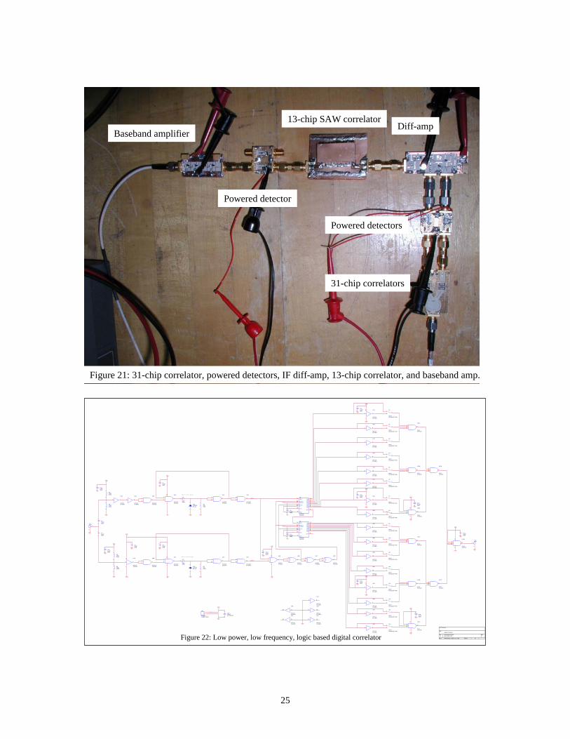
Figure 21: 31-chip correlator, powered detectors, IF diff-amp, 13-chip correlator, and baseband amp.
31-chip correlators
Powered detectors
Diff-amp13-chip SAW correlator
Powered detector
Baseband amplifier
S8
SPDTCAS120JCT-ND
21
3
U4D
AHC3214-SOIC
12
1311
Set to 200ns delay
U1A
AHC1414-SOIC
1 2
147
U9C
AHC1414-SOIC
5 6
U7F
AHC1414-SOIC
13 12
U2A
AHC13214-SOIC
1
23
147
JinSMA
1
2
U7A
AHC1414-SOIC
1 2
147
U9E
AHC1414-SOIC
1110
+ C19100uFEIA7343-31
12
S16
SPDTCAS120JCT-ND
21
3
U7E
AHC1414-SOIC
11 10
U12C
AC1114-SOIC
91011
8
R3100k0402
12
U1E
AHC1414-SOIC
11 10
S5
SPDTCAS120JCT-ND
21
3
U1B
AHC1414-SOIC
3 4
U12B
AC1114-SOIC
345
6
U7B
AHC1414-SOIC
3 4
U1F
AHC1414-SOIC
13 12
U6
AHC59516-SOIC
14 151
11 210 3
412 513 6
7
916
8
SER QAQB
SRCLK QCSRCLR QD
QERCLK QFG QG
QH
QH'VCC
GND
VCC
S4
SPDTCAS120JCT-ND
21
3
U8A
AHC1414-SOIC
1 2
147
3.3v
C90.1uF0603
12
U3B
AHC13214-SOIC
4
56
U9D
AHC1414-SOIC
9 8
U7C
AHC1414-SOIC
5 6
C40.1uF0603
12
VCC
U5
AHC59516-SOIC
14 151
11 210 3
412 513 6
7
916
8
SER QAQB
SRCLK QCSRCLR QD
QERCLK QFG QG
QH
QH'VCC
GND
U1C
AHC1414-SOIC
5 6
U2C
AHC13214-SOIC
9
108
C180.1uF0603
12
C170.1uF0603
12
VCC
VCC
JP1
POWER100MIL PADS
12
C130.1uF0603
12
U11C
AC1114-SOIC
91011
8
R4200k0402
12
R220k0402
12
S13
SPDTCAS120JCT-ND
21
3
S3
SPDTCAS120JCT-ND
21
3
U10C
AC1114-SOIC
91011
8
S12
SPDTCAS120JCT-ND
21
3
U2D
AHC13214-SOIC
12
1311
VCC
U3A
AHC13214-SOIC
1
23
147
C140.1uF0603
12
U12A
AC1114-SOIC
12
1312
147
DIGCORR.SCH
Digital Correlator
R.W. Brocato
D
1 1Wednesday, August 11, 2004
Title
Size Document Number Rev
Date: Sheet of
U8B
AHC1414-SOIC
3 4
C20.1uF0603
12
VCC
Set to 200ns delay
R5100k0402
12
S6
SPDTCAS120JCT-ND
21
3
U11B
AC1114-SOIC
345
6
C120.1uF0603
12
VCC
U4B
AHC3214-SOIC
4
56
U9A
AHC1414-SOIC
1 2
147
C5
22pF0603
1 2
S9
SPDTCAS120JCT-ND
21
3
C160.1uF0603
12
C100.1uF0603
12
HiPuls
C110.1uF0603
12
DX21N5818DL-41
12
JoutSMA
1
2
S7
SPDTCAS120JCT-ND
21
3
U7D
AHC1414-SOIC
9 8
VCC
LoPuls
U2B
AHC13214-SOIC
4
56
U4A
AHC3214-SOIC
1
23
147
VCC
U9F
AHC1414-SOIC
1312
R120k0402
12
U3C
AHC13214-SOIC
9
108
U9B
AHC1414-SOIC
3 4
VCC
U11A
AC1114-SOIC
12
1312
147
C70.1uF0603
12
S10
SPDTCAS120JCT-ND
21
3
R6200k0402
12
C80.1uF0603
12
S1
SPDTCAS120JCT-ND
12
3
U8E
AHC1414-SOIC
11 10
C10.1uF0603
12
DX11N5818DL-41
12
U8D
AHC1414-SOIC
9 8
VCC
U8C
AHC1414-SOIC
5 6
U3D
AHC13214-SOIC
12
1311
VCC
U8F
AHC1414-SOIC
13 12
S15
SPDTCAS120JCT-ND
21
3
U10A
AC1114-SOIC
12
1312
147
C60.1uF0603
12
U4C
AHC3214-SOIC
9
108
C3
22pF0603
1 2
S14
SPDTCAS120JCT-ND
21
3
C150.1uF0603
12
VCC
VCC
S11
SPDTCAS120JCT-ND
21
3
U1D
AHC1414-SOIC
9 8
U10B
AC1114-SOIC
345
6
S2
SPDTCAS120JCT-ND
12
3
Figure 22: Low power, low frequency, logic based digital correlator
25
Conclusions Zero-power radio receivers suitable for a variety of different applications were devised, built, and tested. The SAW correlators built for the various zero-power radios exhibited very good levels of performance. However, true zero-power radio performance is only adequate in high signal level applications. Improvements to passive demodulator/ detectors are needed to improve the low signal reception capabilities of the zero-power radio. Significant performance improvements in radio performance were obtained by using very low power detectors and amplifiers. The current SAW correlator-based radios suitable for a wide-range of applications are very low powered receivers, possibly lower than any other comparable technology. True zero-power radio receivers based on SAW correlators are very viable but need improved passive detectors to achieve high levels of sensitivity. References: 1) Ziemer, R.E., and Tranter, W.H., Principles of Communications, Houghton Mifflin Co.,
1976, pp. 311-317. 2) Campbell, Colin K., “Surface Acoustic Wave Devices for Mobile and Wireless
Communication,” Academic Press, San Diego, 1998, p. 11. 3) Lever, K.V., et al, “Analysis of Effect of Fabrication Errors on Performance of Surface-
Acoustic-Wave M-sequence Correlators,” Proc. IEE, Vol. 122, No. 12, Dec. 1975, pp. 1333-1338.
4) Biran, A., “Low-Sidelobe SAW Barker 13 Correlator,” IEEE 1985 Ultrasonics Symp., pp. 149-152.
26
Distribution 8 MS0874 Robert W. Brocato, 1751 5 MS0874 David W. Palmer, 1751 1 MS0874 Glenn D. Omdahl, 1751 1 MS0874 Gregg A. Wouters, 1751 1 MS0874 Matthew A. Montano, 1751 1 MS0874 Emmett J. Gurule, 1751 1 MS0874 Christopher L. Gibson, 1751 1 MS0603 Edwin J. Heller, 1763 1 MS0603 Joel R. Wendt, 1743 1 MS0603 Jonathan D. Blaich, 1763 1 MS0865 Regan W. Stinnett, 1903 1 MS1071 Michael G. Knoll, 1730 1 MS1202 Ann N. Campbell, 5940 2 MS1202 John P. Anthes, 5940 1 MS0574 Robert C. Ghormley, 5945 2 MS1078 Stephen J. Martin, 1707 1 MS0123 LDRD Office, Donna L. Chavez 1 MS0612 Corporate Records, Arlene Lucero 1 MS9018 Central Technical Files, 8945-1 2 MS0899 Technical Library, 9616 1 MS0612 Review and Approval Desk for DOE/OSTI, 9612
27