a microfabricated inductively-coupled plasma …hopwood/jmems-microicp.pdfa microfabricated...
TRANSCRIPT
A Microfabricated Inductively-Coupled Plasma Generator
J. HopwoodDepartment of Electrical and Computer Engineering,
Northeastern University, Boston, MA 02115
ABSTRACT
The design, fabrication, and characterization of a surface micromachinedplasma generator is described for the first time. The plasma is sustained withoutelectrodes by inductively coupling a 450 MHz current into a region of low-pressure gas. Both argon and air plasmas have been generated over a range ofgas pressures from 0.1 torr to 10 torr (13.3 Pa - 1333 Pa). Typically, the powerused to sustain the plasma is 350 mW, although ~1.5 W is required to initiate thedischarge. Network analysis of the plasma generator circuit shows that over99% of the applied RF power can be absorbed by the device. Of this, ~50% isabsorbed by the plasma and the remainder of the power is dissipated as ohmicheating. An argon ion current of up to 4.5 mA/cm2 has been extracted from theplasma and the electron temperature is 52,000 K at 0.1 torr. This plasma sourceis intended for electronic excitation of gas samples so that the presence ofimpurities and toxins may be detected using optical emission spectroscopy.
2
I. Introduction
A miniaturized device for theproduction of gas phase electrons,ions, and electronically excitedatoms is needed for several MEMSapplications including ionizers formicro mass spectrometers,microthrusters1, plasma displays,and micro atomic emissionspectroscopy2. The microfabricatedplasma generator described in thispaper is intended to be used inconjunction with a miniature Fabry-Perot spectrometer3. The completesystem of plasma source andspectrometer function as a micro gasanalyzer by generating excitedatomic and molecular states within agas sample. The constituents of thatsample are then determined basedon the wavelength of photonsemitted from the plasma followingelectronic de-excitation.
Perhaps the most commonlyused microplasma is found in acplasma displays. Although the acplasma display pixel is very compactand relatively simple, the plasma issustained by high secondaryelectron yield electrodes. In achemically-active plasmaenvironment, such as air, theelectrodes become contaminatedand the pixel fails.4 The search for amore robust miniature plasmasource has produced the dcmicrohollow cathode discharge5 anda capacitively-coupled microwaveplasma6. Both of these devices alsohave electrodes that are exposed tothe plasma. The electrodes maybecome oxidized, chemically etched,or sputter-eroded due to contact with
the plasma. In addition, the electricfield that heats the plasma originatesand terminates on the electrodesurfaces. Charged particles in theplasma are therefore acceleratedtoward the electrodes, where theparticles dissipate a substantialfraction of the supplied power. Thismechanism of RF plasma generationis referred to as capacitive coupling.Electrodeless plasma generators, onthe other hand, impress an electricfield that is tangential to the plasmaboundary. This greatly reduces theenergetic bombardment of theplasma chamber and improves theefficiency of plasma generation7.
The inductively-coupledplasma (ICP) is one type ofelectrodeless discharge that is nowwidely used in microfabricationprocesses due to its relativesimplicity, efficient use of power,long lifetime using reactive gases,and low process contamination8.The scaling principles needed toreduce the size of a plasmaprocessing ICP (300 mm diam.,13.56 MHz) to that of a MEMSdevice are described in a previouspublication9 where it is reported thata 5 mm ICP operates efficiently at~450 MHz. In reference 9, miniatureICPs were fabricated by etchingplanar spiral inductors in copper-cladepoxy boards. These prototypegenerators used discrete capacitorsfor impedance matching. This paperreports the microfabrication andtesting of monolithic, miniaturizedICPs fabricated on glass wafersusing surface micromachining10.
3
II. Design
The principle of operation foran inductively-coupled plasma isillustrated by the equivalent circuit11
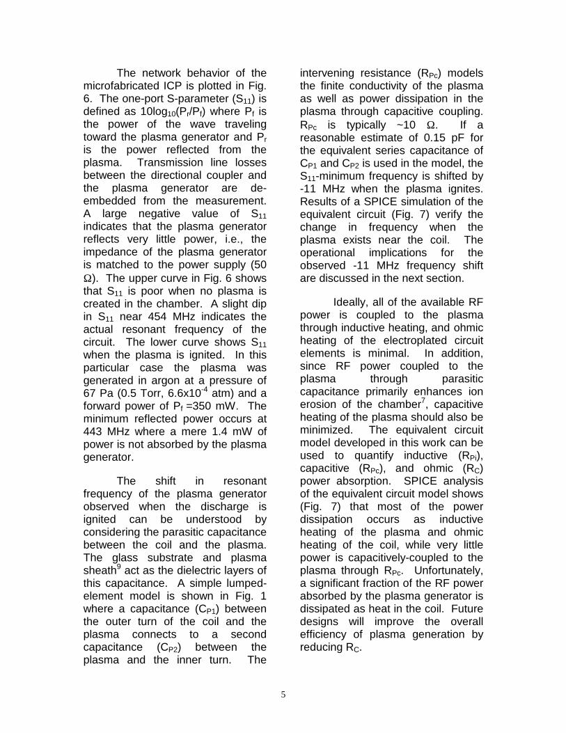
shown in Fig. 1. A planar, spiralinductance (LC) is driven in series-resonance with a capacitance (CT)such that a strong RF magnetic fieldis created near the coil. The plasmaforms in a low-pressure chamberpositioned adjacent to the spiral coil.An electron current flows through theconductive plasma region so as tooppose the RF magnetic fieldgenerated by the coil. The currentflow in the plasma is modeled as asingle-turn inductor (LP) and electroncollisions are modeled as aresistance (RPi). Because the coiland the plasma are adjacent, amutual inductance (M) existsbetween the coil and the plasmainductance. The equivalent circuit,therefore, looks like a nonidealtransformer with a couplingcoefficient k = M/(LCLP)1/2. The RFpower source used to drive thisminiature plasma has a 50Ωcharacteristic impedance. CL is usedto cancel the inductive reactance ofthe circuit and match the impedanceof the plasma to the RF source.
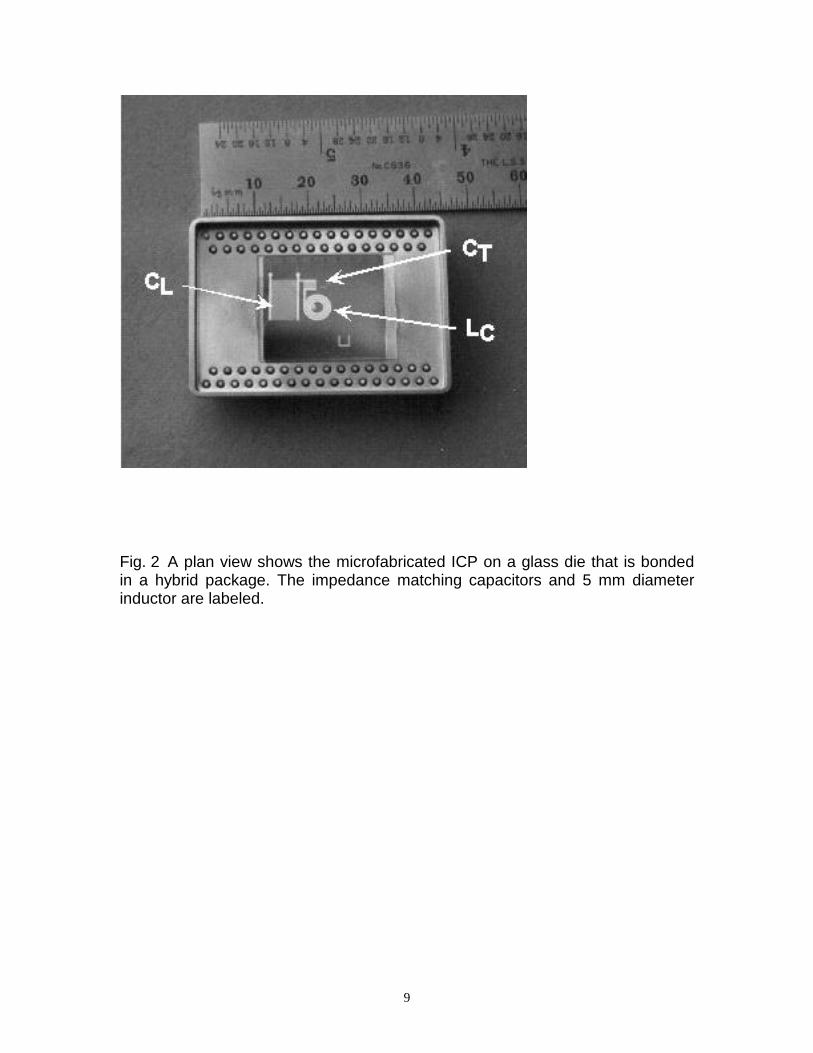
A photograph of the plasmagenerator mounted in a 66-pin hybridpackage is shown in Fig. 2 with thethree microfabricated circuitelements labeled (LC, CT, and CL).The three-turn coil has a diameter of5 mm and each turn is 400 µm widewith a 100 µm gap between turns.The inductance is ~40 nH and theequivalent series resistance of a 7µm-thick coil fabricated in gold is RC
= 0.4 Ω at 450 MHz. The 'tuning'
capacitance (CT) is chosen to be ~3pF such that the LC-series circuitresonates near 450 MHz. The loopof current within the plasma has acalculated inductance of LP ~ 4 nH.The resistance of the plasma aroundthis inductive loop, which dependson the gas pressure and electrondensity12, is the order of RPi = 100 Ω .Power dissipated in RPi representsthe inductively-coupled powerabsorbed by the discharge. Thetransformer coupling coefficient forplanar ICP generators13 is estimatedto be k=0.2. Finally, analysis14 of theequivalent circuit indicates that CLshould be approximately 50 pF.
The microfabricatedcapacitors that form the impedancematching network for the ICP mustbe capable of operating at highvoltage (100s of volts) and highcurrent (~1 A) at a frequency of 450MHz. The capacitors must also havea good quality factor such that powerloss is minimal. Interdigitatedcapacitors on a glass substrate canmeet these criteria and have theadded advantage that only a singlephotomask is needed for fabrication.The width of each digit and the gapbetween digits was chosen to be 10µm based on process constraintsand electrical breakdown strength15.The geometry of each capacitor wasdesigned using the method ofAlley16.
The capacitors and inductorare formed from electroplated gold.The thickness of the electroplatedfilm is based on the skin depth of450 MHz current,
mo µωσµδ 5.3)/2( 2/1 ==
4
where µo and σ are the permeabilityand conductivity of the metal and ω =2πf. Since the current density decaysexponentially from the surface of themetallization, a total plated thicknessof two skin depths (7 µm) was used.Although copper would decrease theparasitic resistance of the plasmagenerator, experience shows thatcopper also oxidizes quickly. Thesegold structures, however, haveoperated in unsealed packages for atleast 3 months.
III. Fabrication and Packaging
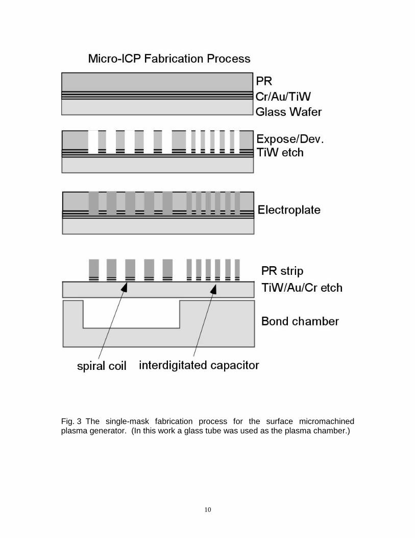
The fabrication sequence,shown in Fig. 3, begins with thesputter deposition of a 30 nm Cradhesion layer, a 100 nm Au seedlayer, and a 30 nm TiW adhesionlayer on a 700 µm thick glass wafer.A double spin coat of Shipley 4620photoresist forms a 15 µm thickplating mold after exposure anddevelop. The TiW adhesion layer isetched to expose the Au seed layerfrom which 7 µm-thick goldmicrostructures are electroplated.The process is completed bystripping the photoresist and etchingthe initial sputtered layers using theelectroplated features as a mask.The fabrication of the plasma sourceonly requires a single photomask,eliminating the need for maskalignment.
The wafers are diced andindividual die are bonded into hybridpackages that are cut withrectangular windows as shown inFig. 2. Two wire bonds connect therf power input from the package tothe die and a third wire bond is usedto crossover from the inner turn of
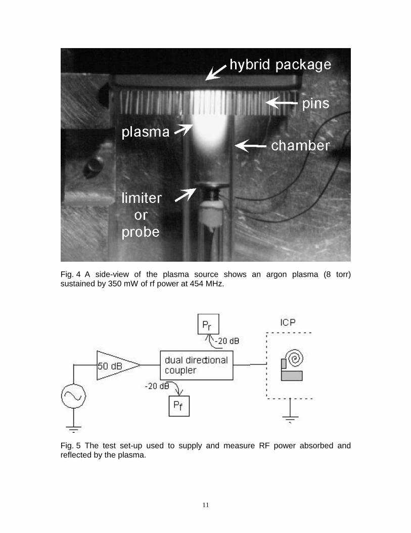
the inductor to CL. Later versions ofthe plasma generator will havebonded chambers withmicrofabricated gas inlets andpumping. So that the plasmabehavior can be measured, however,this circuit is bonded to a 9-mm i.d.glass tube as shown in Fig. 4. Theglass die forms an endcap for thetube with the circuit components onthe outside. The tube connects theplasma generator to a conventionalvacuum system that is equipped witha high-accuracy capacitancemanometer for pressuremeasurement. A Langmuir probemay be inserted through the tubeand into the plasma to determine itsion density and electrontemperature.
IV. Experiment and Results
A. Network Analysis
Ultimately, it is envisioned thatthe plasma generator will be drivenby an integrated circuit oscillatorbonded within the hybrid package.For the purpose of experimentalcharacterization, however, precisionRF instrumentation is used to supplypower to the plasma. Figure 5shows a block diagram of the RFpower supply and measurementsystem. The power source consistsof an HP 8656A (1 MHz-990 MHz)signal generator and an ENI 525LAlinear amplifier (gain = 50 dB, 1-500MHz). The forward power andreflected power are measured usinga Narda 3020A dual-directionalcoupler and HP 435A RF powermeter. The ICP is placed in a small,grounded aluminum box. Allelectrical connections are made with50 Ω coaxial cable.
5
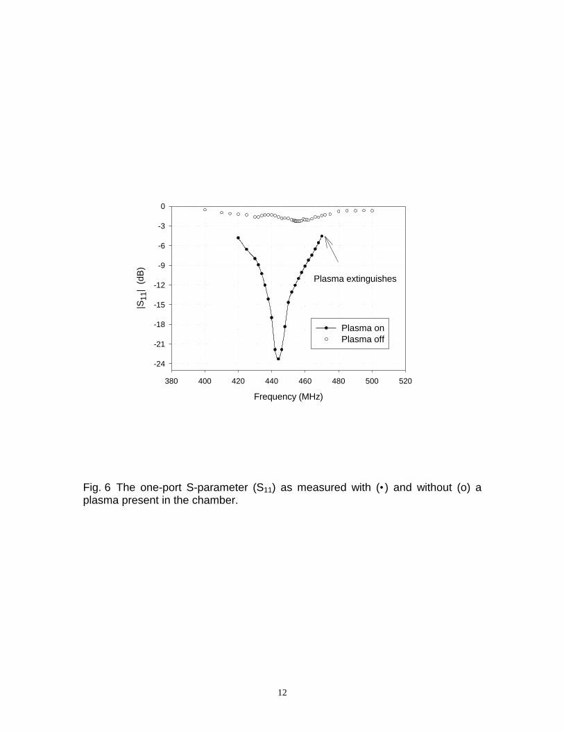
The network behavior of themicrofabricated ICP is plotted in Fig.6. The one-port S-parameter (S11) isdefined as 10log10(Pr/Pf) where Pf isthe power of the wave travelingtoward the plasma generator and Pris the power reflected from theplasma. Transmission line lossesbetween the directional coupler andthe plasma generator are de-embedded from the measurement.A large negative value of S11indicates that the plasma generatorreflects very little power, i.e., theimpedance of the plasma generatoris matched to the power supply (50Ω ). The upper curve in Fig. 6 showsthat S11 is poor when no plasma iscreated in the chamber. A slight dipin S11 near 454 MHz indicates theactual resonant frequency of thecircuit. The lower curve shows S11when the plasma is ignited. In thisparticular case the plasma wasgenerated in argon at a pressure of67 Pa (0.5 Torr, 6.6x10⁻⁴ atm) and aforward power of Pf =350 mW. Theminimum reflected power occurs at443 MHz where a mere 1.4 mW ofpower is not absorbed by the plasmagenerator.
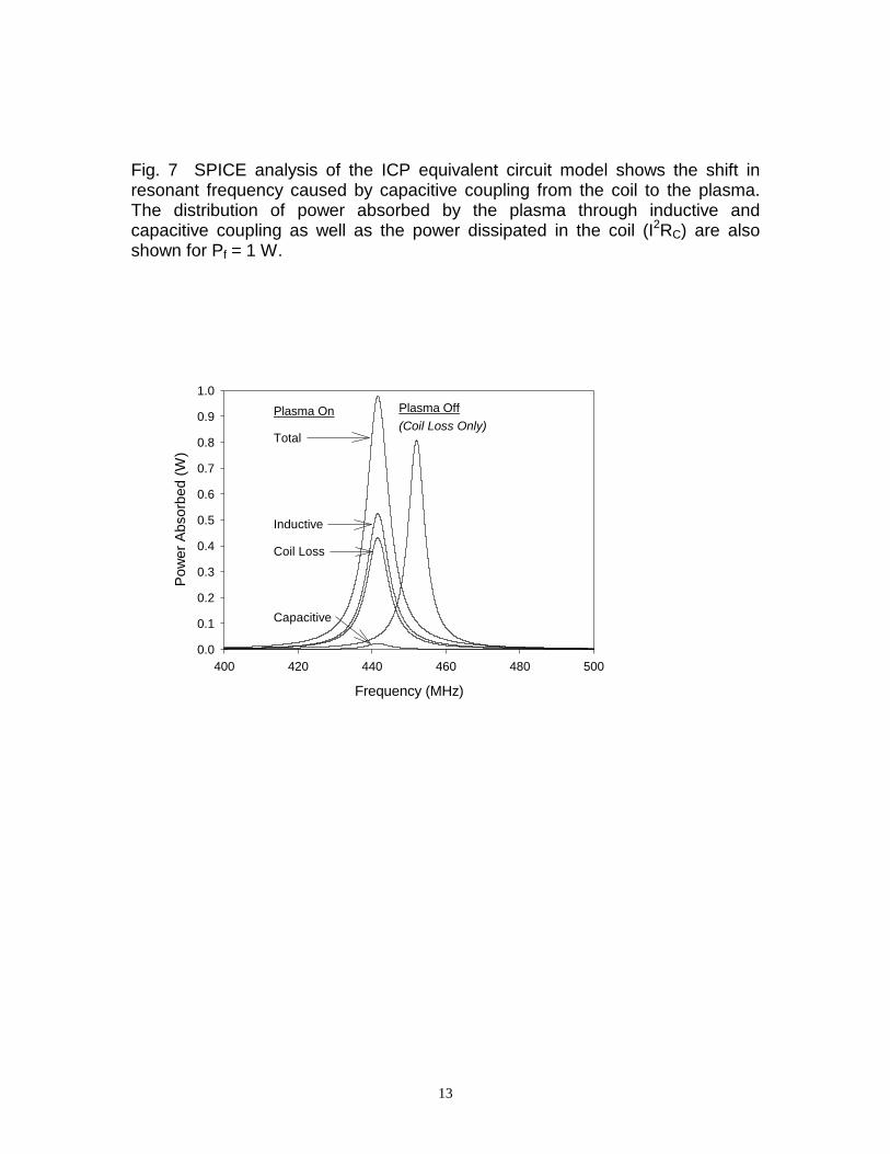
The shift in resonantfrequency of the plasma generatorobserved when the discharge isignited can be understood byconsidering the parasitic capacitancebetween the coil and the plasma.The glass substrate and plasmasheath9 act as the dielectric layers ofthis capacitance. A simple lumped-element model is shown in Fig. 1where a capacitance (CP1) betweenthe outer turn of the coil and theplasma connects to a secondcapacitance (CP2) between theplasma and the inner turn. The
intervening resistance (RPc) modelsthe finite conductivity of the plasmaas well as power dissipation in theplasma through capacitive coupling.RPc is typically ~10 Ω . If areasonable estimate of 0.15 pF forthe equivalent series capacitance ofCP1 and CP2 is used in the model, theS11-minimum frequency is shifted by-11 MHz when the plasma ignites.Results of a SPICE simulation of theequivalent circuit (Fig. 7) verify thechange in frequency when theplasma exists near the coil. Theoperational implications for theobserved -11 MHz frequency shiftare discussed in the next section.
Ideally, all of the available RFpower is coupled to the plasmathrough inductive heating, and ohmicheating of the electroplated circuitelements is minimal. In addition,since RF power coupled to theplasma through parasiticcapacitance primarily enhances ionerosion of the chamber7, capacitiveheating of the plasma should also beminimized. The equivalent circuitmodel developed in this work can beused to quantify inductive (RPi),capacitive (RPc), and ohmic (RC)power absorption. SPICE analysisof the equivalent circuit model shows(Fig. 7) that most of the powerdissipation occurs as inductiveheating of the plasma and ohmicheating of the coil, while very littlepower is capacitively-coupled to theplasma through RPc. Unfortunately,a significant fraction of the RF powerabsorbed by the plasma generator isdissipated as heat in the coil. Futuredesigns will improve the overallefficiency of plasma generation byreducing RC.
6
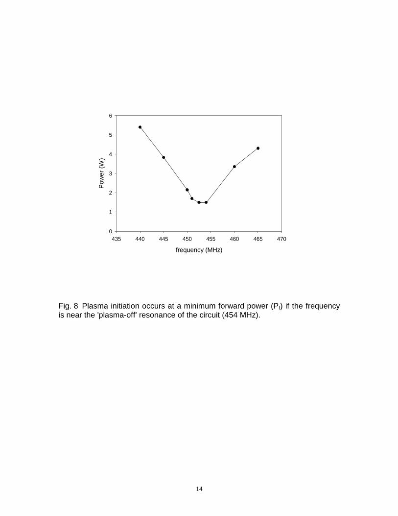
B. Plasma Ignition
Since the power budget of aMEMS device is limited, theminimum forward power required forplasma initiation was measured as afunction of power source frequencyand gas pressure in the chamber.Generally, ICPs ignite bycapacitively-coupling the highvoltage present at the terminals ofthe unloaded LCCT tank circuit intothe chamber. It should be noted thatonce the plasma is established, theinductive power required to sustainthe plasma is always considerablylower than the initiation power.Therefore, the RF power supplymust be sized to ensure that thedischarge starts. In Fig. 8 theplasma is shown to ignite at Pf = 1.5W if the frequency is close to the'plasma-off' resonance, but thepower requirement increases rapidlyfor higher and lower frequencies. Itis interesting to note an advantage oftransforming the plasma impedanceusing an ICP: a 1.5 W RF oscillator(Z=50Ω ) only requires a voltageswing of ±12 v, which is far less thanthe hundreds of volts needed toinitiate other small plasmagenerators.
The frequency shift caused bythe parasitic capacitance betweenthe coil and the plasma may affectthe design of the RF supply. Asophisticated RF power source mightincrease its operating frequency toinitiate the plasma and then reducethe frequency to obtain the bestpower absorption. The moresimplistic solution of fixing thefrequency to minimize initiationpower, however, is also reasonablebecause S11 is still -10 dB at 454
MHz with the plasma on (see Figs. 4and 6). That is, only 10% of theforward power is reflected from theplasma. The additional electroniccomplexity needed to gain 10% inplasma source performance may notbe warranted for many applications.
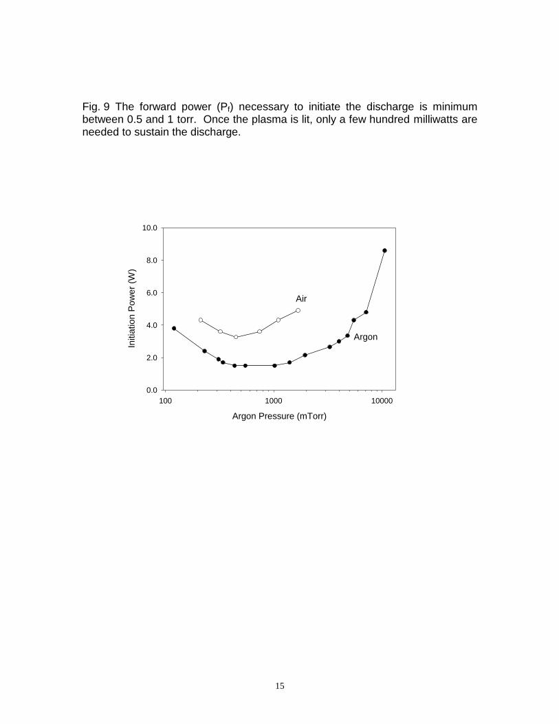
This plasma generator isintended to operate at gas pressureswell below one atmosphere.Because the gas pumping speed ofvacuum MEMS devices will likely bequite limited, we have investigatedthe performance of the plasmagenerator as a function of gaspressure. Figure 9 shows theplasma initiation power in argon as afunction of gas pressure from 0.1 torrto 10 torr (13 - 1333 Pa). Although itis possible to ignite the dischargeover this entire range, it is clearlyeasier to start the discharge in thevicinity of 1 torr (133 Pa). In aprevious publication9 it was shownthat the plasma ignites most readilywhen the power source frequency(ω) equals the electron-neutralcollision frequency17 (v) in theplasma. The electron collisionfrequency scales linearly with thegas density and therefore with gaspressure. For ω = 2π x 450 MHz, thecollision frequency is optimum at anargon pressure of 0.8 torr, which isconsistent with the experimentalresult shown in Fig. 9. If it isdesirable to initiate the plasma at ahigher pressure, the plasmagenerator should be designed tooperate at a proportionally higherfrequency.
The upper curve in Fig. 9shows that the forward powerrequired to ignite an air plasma istwice that of an Ar plasma. This is
7
consistent with published data18
showing that the microwave electricfield breakdown strength of argon is35 V/cm, but the breakdown fieldincreases to 70 V/cm in air. Thedata of Fig. 9 also show that theoptimum pressure for air breakdownis below that of argon. This result isconsistent with Ref. 18.
C. Plasma Properties
A cylindrical tungsten probe,called a Langmuir probe19, wasinserted into the plasma to measurethe electron temperature and theextractable ion current density. Anion current of 1 mA/cm2 could beextracted from an argon discharge atPf = 350 mW. The ion currentdensity increased to 4.5 mA/cm2 atPf = 4W. From Langmuir probetheory, this corresponds to an iondensity of ~1011 cm-3. The electrontemperature was consistent withearlier results9, decreasing from52,000 K (4.5 eV) at 0.1 torr to25,000 K (2.2 eV) at 1.1 torr. A morecomplete plasma characterizationstudy can be found elsewhere20.
V. Conclusion
For the first time, a surfacemicromachined inductively-coupled
plasma generator has produced bothargon and air discharges. Thedevice is simple to fabricate androbust. The plasma generator hasremained functional after threemonths' exposure to a non-cleanroom environment andoperation using inert and oxidizinggases. Presently power is suppliedfrom laboratory instrumentation, butRF power circuits similar to thoseused in personal wirelesscommunications are more thanadequate for initiating and sustainingthis plasma. In the future, we willcontinue to scale the diameter of thecoil and plasma chamber towarddimensions of 1 mm or less.
Acknowledgments
The author wishes to thank Mr.Weilin Hu, Mr. Richard Morrison, andMr. Yu Yin for their assistance, andMr. Keith Warner and Prof. NicolMcGruer for critical reviews of themanuscript. This work wassupported by the National ScienceFoundation under Grant No. ECS-9701916.
8
Fig. 1 The equivalent circuit of an inductively-coupled plasma consists of animpedance matching network (CL and CT) and an inductive coupler (LC).Theplasma is modeled as a single current loop with inductance LP and resistanceRCi. The remaining elements are parasitic (see text).
9
Fig. 2 A plan view shows the microfabricated ICP on a glass die that is bondedin a hybrid package. The impedance matching capacitors and 5 mm diameterinductor are labeled.
10
Fig. 3 The single-mask fabrication process for the surface micromachinedplasma generator. (In this work a glass tube was used as the plasma chamber.)
11
Fig. 4 A side-view of the plasma source shows an argon plasma (8 torr)sustained by 350 mW of rf power at 454 MHz.
Fig. 5 The test set-up used to supply and measure RF power absorbed andreflected by the plasma.
12
Fig. 6 The one-port S-parameter (S11) as measured with (•) and without (o) aplasma present in the chamber.
Frequency (MHz)
380 400 420 440 460 480 500 520
|S11
| (d
B)
-24
-21
-18
-15
-12
-9
-6
-3
0
Plasma onPlasma off
Plasma extinguishes
13
Fig. 7 SPICE analysis of the ICP equivalent circuit model shows the shift inresonant frequency caused by capacitive coupling from the coil to the plasma.The distribution of power absorbed by the plasma through inductive andcapacitive coupling as well as the power dissipated in the coil (I2RC) are alsoshown for Pf = 1 W.
Frequency (MHz)
400 420 440 460 480 500
Pow
er A
bsor
bed
(W)
0.0
0.1
0.2
0.3
0.4
0.5
0.6
0.7
0.8
0.9
1.0Plasma Off (Coil Loss Only)
Total
Inductive
Coil Loss
Capacitive
Plasma On
14
Fig. 8 Plasma initiation occurs at a minimum forward power (Pf) if the frequencyis near the 'plasma-off' resonance of the circuit (454 MHz).
frequency (MHz)
435 440 445 450 455 460 465 470
Pow
er (W
)
0
1
2
3
4
5
6
15
Fig. 9 The forward power (Pf) necessary to initiate the discharge is minimumbetween 0.5 and 1 torr. Once the plasma is lit, only a few hundred milliwatts areneeded to sustain the discharge.
Argon Pressure (mTorr)
100 1000 10000
Initi
atio
n P
ower
(W)
0.0
2.0
4.0
6.0
8.0
10.0
Air
Argon
16
REFERENCES
1 J. Mueller, J. R. Brophy, J. E. Polk, and J. J. Blandino, “The JPL ion thruster-on-a-chip concept,” 7th NASA-OSAT Advanced Space Propulsion Workshop,Pasadena, CA, April 10, 1996.
2 B. S. Ross, D. M. Chambers, G. H. Vickers, P. Yang and G. M. Hieftje,“Characterisation of a 9-mm torch for inductively coupled plasma massspectrometry,” J. Anal. At. Spectrom., vol. 5, pp. 351-358, 1990.
3 P.M. Zavracky, K. L. Denis, H.K. Xie, R. Grace, T. Wester, “A MicromachinedScanning Fabry-Perot Interferometer,” Proceedings of SPIE, vol. 3514, pp. xxx-yyy, Nov. 1998.
4 R.M. Caloi and C. Carretti, "Getters and gettering in plasma display panels," J.Vac. Sci. Technol. A, vol. 16, pp. 1991-1996, 1998.
5 K. H. Schoenbach, C. A. Verhappen, T. Tessnow, F. E. Peterskin, and W. W.Byszewski, "Microhollow cathode discharges, " Appl. Phys. Lett., vol. 68, no. 1,pp. 13-15, 1996.
6 P. Siebert, G. Petzold, A. Hellenbart, J. Muller, "Surfacemicrostructure/miniature mass spectrometer: processing and applications," Appl.Phys. A, vol. 67, pp. 155-160, 1998.
7 M. A. Lieberman and A. J. Lichtenberg, Principals of Plasma Discharges andMaterials Processing, New York: Wiley, 1994, p. 308-309.
8 J. Hopwood, "Review of inductively coupled plasmas for plasma processing,"Plasma Sources Science and Technology, vol. 1, no. 2, pp. 109-116, 1992.
9 Y. Yin, J. Messier, and J. Hopwood, "Miniaturization of inductively coupledplasma sources," IEEE Trans. Plasma Sci., vol. 27, no. 5, pp. 1516-1524, 1999.
10 "Monolithic miniaturized inductively coupled plasma source," J. Hopwood, U.S.Patent No. 5,942,855 (August 24, 1999).
11 R. B. Piejak, V. A. Godyak, and B. M. Alexandrovich, “A simple analysis of aninductive RF discharge,” Plasma Sources Sci. Technol., vol. 1, pp. 179-1861992.
12 M. A. Lieberman and A. J. Lichtenberg, Principals of Plasma Discharges andMaterials Processing, New York: Wiley, 1994, p. 392.
13 L. J. Mahoney, Ph. D. Thesis, University of Wisconsin-Madison, p.51 (1994).

17
14 M. A. Lieberman and A. J. Lichtenberg, Principals of Plasma Discharges andMaterials Processing, New York: Wiley, 1994, p. 396.
15 J. D. Craggs, "High-frequency Breakdown of Gases," in Electrical Breakdownof Gases, Meeks and Grayyh, Eds., New York: Wiley, 1973, pp.689-705.
16 G. D. Alley, "Interdigital capacitors and their application to lumped-elementmicrowave integrated circuits," IEEE Trans. on Microwave Theory and Tech., vol.MTT-18, no. 12, pp. 1028-1033, 1970.
17 M. A. Lieberman and A. J. Lichtenberg, Principals of Plasma Discharges andMaterials Processing, New York: Wiley, 1994, p. 80.
18 S. C. Brown, Basic Data of Plasma Physics, Cambridge, MA: The MIT Press,1966, p. 252.
19 I.D. Sudit and R.C. Woods, J. Appl. Phys. vol. 76, pp. 4488, 1994.
20 J. Hopwood, J. Vac. Sci. Technol., in preparation.