a fully integrated 8-channel closed-loop neural-prosthetic cmos soc for real-time epileptic seizure...
TRANSCRIPT

232 IEEE JOURNAL OF SOLID-STATE CIRCUITS, VOL. 49, NO. 1, JANUARY 2014
A Fully Integrated 8-Channel Closed-LoopNeural-Prosthetic CMOS SoC for Real-Time
Epileptic Seizure ControlWei-Ming Chen, Member, IEEE, Herming Chiueh, Member, IEEE, Tsan-Jieh Chen, Member, IEEE, Chia-Lun Ho,Chi Jeng, Ming-Dou Ker, Fellow, IEEE, Chun-Yu Lin, Member, IEEE, Ya-Chun Huang, Chia-Wei Chou,Tsun-Yuan Fan, Ming-Seng Cheng, Yue-Loong Hsin, Sheng-Fu Liang, Member, IEEE, Yu-Lin Wang,Fu-Zen Shaw, Yu-Hsing Huang, Chia-Hsiang Yang, Member, IEEE, and Chung-Yu Wu, Fellow, IEEE
Abstract—An 8-channel closed-loop neural-prosthetic SoC ispresented for real-time intracranial EEG (iEEG) acquisition,seizure detection, and electrical stimulation in order to suppressepileptic seizures. The SoC is composed of eight energy-efficientanalog front-end amplifiers (AFEAs), a 10-b delta-modulatedSAR ADC (DMSAR ADC), a configurable bio-signal processor(BSP), and an adaptive high-voltage-tolerant stimulator. A wire-
Manuscript received April 22, 2013; revised September 11, 2013; acceptedSeptember 12, 2013. Date of publication October 18, 2013; date of currentversion December 20, 2013. This paper was approved by Guest EditorMichiel Pertijs. This work was supported in part by the National ScienceCouncil (NSC), R.O.C., under Project 102-2220-E-009-001 and by the “Aimfor the Top University Plan” of the National Chiao Tung University andMinistry of Education, Taiwan, R.O.C.W.-M. Chen, M.-D. Ker, C.-H. Yang, and C.-Y. Wu are with the Department
of Electronics Engineering and the Institute of Electronics, National Chiao TungUniversity, Hsinchu 300, Taiwan, and also with the Biomedical ElectronicsTranslational Research Center, National Chiao Tung University, Hsinchu 300,Taiwan (e-mail: [email protected]; [email protected]).H. Chiueh and T.-J. Chen are with the Department of Electrical and Computer
Engineering, National Chiao Tung University, Hsinchu 300, Taiwan, and alsowith the Biomedical Electronics Translational Research Center, National ChiaoTung University, Hsinchu 300, Taiwan, and also with the Biomedical Elec-tronics Translational Research Center, National Chiao TungUniversity, Hsinchu300, Taiwan (e-mail: [email protected]).C.-L. Ho and C. Jeng are with the Department of Electrical and Computer
Engineering, National Chiao Tung University, Hsinchu 300, Taiwan.C.-Y. Lin is with the Department of Applied Electronics Technology, Na-
tional TaiwanNormal University, Taipei 106, Taiwan, and alsowith the Biomed-ical Electronics Translational Research Center, National Chiao TungUniversity,Hsinchu 300, Taiwan (e-mail: [email protected]).Y.-C. Huang, C.-W. Chou, T.-Y. Fan, and M.-S. Cheng are with the Depart-
ment of Electronics Engineering and the Institute of Electronics, National ChiaoTung University, Hsinchu 300, Taiwan.Y.-L. Hsin is with Chung Shan Medical University Hospital, Taichung
402, Taiwan, and also with the Biomedical Electronics Translational ResearchCenter, National Chiao Tung University, Hsinchu 300, Taiwan (e-mail:[email protected]).S.-F. Liang is with the Department of Computer Science and Information
Engineering and Institute of Medical Informatics, National Cheng Kung Uni-versity, Tainan 701, Taiwan, and also with the Biomedical Electronics Transla-tional Research Center, National Chiao Tung University, Hsinchu 300, Taiwan(e-mail: [email protected]).Y.-L. Wang is with the Biomedical Electronics Translational Research
Center, National Chiao Tung University, Hsinchu 300, Taiwan (e-mail:[email protected]).F.-Z. Shaw is with the Department of Psychology and Institute of Geron-
tology National Cheng Kung University, Tainan 701, Taiwan, and also withthe Biomedical Electronics Translational Research Center, National Chiao TungUniversity, Hsinchu 300, Taiwan (e-mail: [email protected]).Y.-H. Huang is with the Department of Psychology, National Cheng Kung
University, Tainan 701, Taiwan (e-mail: [email protected]).Color versions of one or more of the figures in this paper are available online
at http://ieeexplore.ieee.org.Digital Object Identifier 10.1109/JSSC.2013.2284346
less power-and-data transmission system is also embedded. Byleveraging T-connected pseudo-resistors, the high-pass (low-pass)cutoff frequency of the AFEAs can be adjusted from 0.1 to 10 Hz(0.8 to 7 kHz). The noise-efficiency factor (NEF) of the AFEA is1.77, and the DMSAR ADC achieves an ENOB of 9.57 bits. TheBSP extracts the epileptic features from time-domain entropyand frequency spectrum for seizure detection. A constant 30- Astimulus current is delivered by closed-loop control. The acquiredsignals are transmitted with on-off keying (OOK) modulation at4 Mbps over the MedRadio band for monitoring. A multi-LDOtopology is adopted to mitigate the interferences across differentpower domains. The proposed SoC is fabricated in 0.18- mCMOS and occupies 13.47 mm . Verified on Long Evans rats,the proposed SoC dissipates 2.8 mW and achieves high detectionaccuracy 92% within 0.8 s.
Index Terms—Closed-loop control, epilepsy, neuron modula-tion, neural prosthesis, system-on-Chip (SoC), wireless powertransmission.
I. INTRODUCTION
E PILEPSY is a one of the common neurological disorders.Around 1% of the world population is affected. Epileptic
seizures are caused by sudden excessive electrical dischargesin a group of cortical neurons. It is characterized by recurrentseizures, which may vary from a brief lapse of attention andunnatural posturing to severe and prolonged convulsions. Theunexpected seizures impact the quality of life for patients andtheir families.Currently, numerous anti-epileptic drugs are available for
seizure control, but approximately 30% of epileptic patientsremain either drug-resistant or develop limiting adverse effects[1]. Conventional resection surgery might be beneficial to pa-tients who respond poorly to medical treatment. However, onlysome patients are suitable for resection surgery. The possibilityof obtaining undesired neurologic deficits is always a concern.Electrical neuromodulation to control drug-resistant epilepsyhas been attempted due to several potential advantages overconventional surgery, such as its reversible characteristic [2],[3].In addition to peripheral vagus nerve stimulation, prelimi-
nary results show that electrical stimulation on the central ner-vous system is a promising solution, which is still under de-velopment. It delivers electrical impulses to a selected brainregion in response to detected epileptic or pre-epileptic activi-ties [4]. Preferably, a neural-prosthetic device realizing a recip-
0018-9200 © 2013 IEEE
CHEN et al.: FULLY INTEGRATED 8-CHANNEL CLOSED-LOOP NEURAL-PROSTHETIC CMOS SOC FOR REAL-TIME EPILEPTIC SEIZURE CONTROL 233
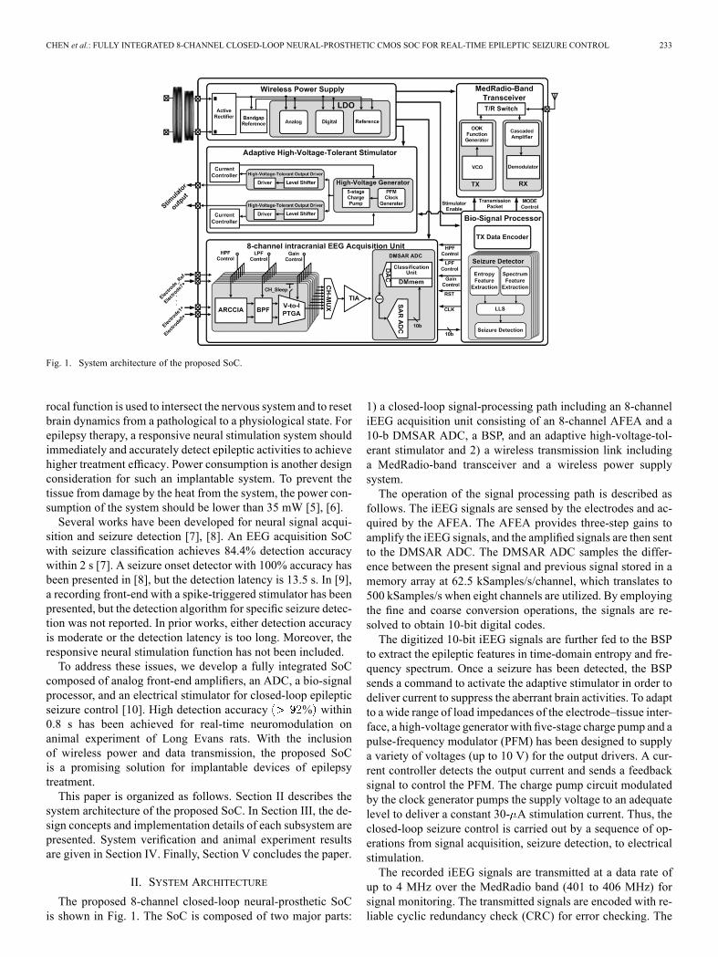
Fig. 1. System architecture of the proposed SoC.
rocal function is used to intersect the nervous system and to resetbrain dynamics from a pathological to a physiological state. Forepilepsy therapy, a responsive neural stimulation system shouldimmediately and accurately detect epileptic activities to achievehigher treatment efficacy. Power consumption is another designconsideration for such an implantable system. To prevent thetissue from damage by the heat from the system, the power con-sumption of the system should be lower than 35 mW [5], [6].Several works have been developed for neural signal acqui-
sition and seizure detection [7], [8]. An EEG acquisition SoCwith seizure classification achieves 84.4% detection accuracywithin 2 s [7]. A seizure onset detector with 100% accuracy hasbeen presented in [8], but the detection latency is 13.5 s. In [9],a recording front-end with a spike-triggered stimulator has beenpresented, but the detection algorithm for specific seizure detec-tion was not reported. In prior works, either detection accuracyis moderate or the detection latency is too long. Moreover, theresponsive neural stimulation function has not been included.To address these issues, we develop a fully integrated SoC
composed of analog front-end amplifiers, an ADC, a bio-signalprocessor, and an electrical stimulator for closed-loop epilepticseizure control [10]. High detection accuracy % within0.8 s has been achieved for real-time neuromodulation onanimal experiment of Long Evans rats. With the inclusionof wireless power and data transmission, the proposed SoCis a promising solution for implantable devices of epilepsytreatment.This paper is organized as follows. Section II describes the
system architecture of the proposed SoC. In Section III, the de-sign concepts and implementation details of each subsystem arepresented. System verification and animal experiment resultsare given in Section IV. Finally, Section V concludes the paper.
II. SYSTEM ARCHITECTURE
The proposed 8-channel closed-loop neural-prosthetic SoCis shown in Fig. 1. The SoC is composed of two major parts:
1) a closed-loop signal-processing path including an 8-channeliEEG acquisition unit consisting of an 8-channel AFEA and a10-b DMSAR ADC, a BSP, and an adaptive high-voltage-tol-erant stimulator and 2) a wireless transmission link includinga MedRadio-band transceiver and a wireless power supplysystem.The operation of the signal processing path is described as
follows. The iEEG signals are sensed by the electrodes and ac-quired by the AFEA. The AFEA provides three-step gains toamplify the iEEG signals, and the amplified signals are then sentto the DMSAR ADC. The DMSAR ADC samples the differ-ence between the present signal and previous signal stored in amemory array at 62.5 kSamples/s/channel, which translates to500 kSamples/s when eight channels are utilized. By employingthe fine and coarse conversion operations, the signals are re-solved to obtain 10-bit digital codes.The digitized 10-bit iEEG signals are further fed to the BSP
to extract the epileptic features in time-domain entropy and fre-quency spectrum. Once a seizure has been detected, the BSPsends a command to activate the adaptive stimulator in order todeliver current to suppress the aberrant brain activities. To adaptto a wide range of load impedances of the electrode–tissue inter-face, a high-voltage generator with five-stage charge pump and apulse-frequency modulator (PFM) has been designed to supplya variety of voltages (up to 10 V) for the output drivers. A cur-rent controller detects the output current and sends a feedbacksignal to control the PFM. The charge pump circuit modulatedby the clock generator pumps the supply voltage to an adequatelevel to deliver a constant 30- A stimulation current. Thus, theclosed-loop seizure control is carried out by a sequence of op-erations from signal acquisition, seizure detection, to electricalstimulation.The recorded iEEG signals are transmitted at a data rate of
up to 4 MHz over the MedRadio band (401 to 406 MHz) forsignal monitoring. The transmitted signals are encoded with re-liable cyclic redundancy check (CRC) for error checking. The

234 IEEE JOURNAL OF SOLID-STATE CIRCUITS, VOL. 49, NO. 1, JANUARY 2014
encoded data are then sent to an OOK modulator. At the re-ceiver, cascaded gain stages and a four-input current-mode en-velope detector are used to recover the signals.For an implanted system supported by a battery, the voltage
of the battery decrease as time passes after implantation, andthus the signal quality and system performance of the implantedsystem are degraded. Moreover, frequent surgery for battery re-placement increases the risk for the patients. Therefore, a wire-less power supply system has been designed to supply a steadypower to the implanted device and hence maintain signal qualityand system performance. A rechargeable battery can also be im-planted to be a backup power source for the implanted system.The required power of the SoC is transmitted through induc-tive coils. The wireless power supply system includes a pair ofcoils with a resonance frequency of 13.56 MHz, an active rec-tifier, and three low-dropout regulators (LDOs). In the activerectifier, two delay comparators are used to compensate bothgate turn-on and turn-off delay times of the power MOS de-vices to achieve a conversion efficiency of 84.8%. Amulti-LDOtopology is adopted to mitigate interferences across differentpower domains.
III. CIRCUIT DESIGN
Here, the 8-channel aquisition unit, the bio-signal processor,and the adaptive high-voltage-tolerant stimulator are describedfirst. The other two additional subsections describe the sup-porting units: the MedRadio-band transceiver and the inductivelink power supply system.
A. 8-Channel Acquisition Unit
The architecture of the 8-channel acquisition unit is describedin Fig. 1. It consists of an 8-channel AFEA and a DMSARADC. The 8-channel AFEA consist of eight auto-reset capac-itive-coupled instrumentation amplifiers (ARCCIAs), config-urable bandpass filters (BPFs), power-gating programmabletransconductance gain amplifiers (PTGA), a multiplexer, anda shared transimpedance amplifier (TIA). Each AFEA channelis implemented by using two cascaded stages. The first stage isthe ARCCIA with a low-noise amplifier and an auto-reset unit(ARU) followed by a BPF to provide a 40-dB gain. The ARUdetects the range of the output of the ARCCIA and provides anadditional path to prevent saturation of the AFEA by electricalstimulation or other extra injection charges. Hence, periodicreset or auto-zeroing, which degrades the high-pass frequency,can be avoided. With the use of the proposed T-connectedpseudo-resistor (TPR), a low high-pass cutoff frequency canbe realized with lower impedance to ensure the stability of theAFEA. The second stage includes the PTGA and TIA, whichprovide additional gains for proper voltage-level adjustment.All passive components and bias circuits are designed on chipto avoid off-chip components and to achieve better matchingcharacteristics.1) Analog Front-End Amplifier: In the neural-prosthesis SoC
for implantable devices, the acquired iEEG signals have thecharacteristics of small amplitude (0.05–1 mV), low frequency(0–200 Hz), and low signal-to-noise ratio [11], [12]. Thus, theAFEA must meet the following design requirements.
Fig. 2. Structure of the ARCCIA.
Fig. 3. (a) Schematic of implemented with TPR and the equivalentmodel. (b) Schematic of the conventional pseudo-resistor and the equivalentmodel.
1) The power consumption should beminimized to extend thesystem lifetime and to reduce the heat to prevent damagingthe surrounding tissues by heating.
2) The noise rejection ability should be high to reduce outputnoise from sources including power-line interference andelectrically or magnetically induced interference.
3) The electrode dc offset (EDO) should be eliminated to pre-vent saturation of the succeeding amplifier. An ultra-lowhigh-pass cutoff frequency must be realized to filter out theEDO and prevent in-band signal degradation.
The first stage of the AFEA is an ARCCIA combined with aBPF. As shown in Fig. 2, capacitors at the input node blockout any EDO from the electrode–tissue interface. The ac-cou-pled signal is further amplified by a succeeding low-noise am-plifier. The low-noise amplifier has a fully differential operationamplifier (OP) which includes a capacitor and a resistor in par-allel as a feedback circuit. The-fully differential OP amplifier
is employed to improve both common-mode rejection ratio(CMRR) and linearity. The differential input and output swingsof are designed as 10 mVp-p and 1 Vp-p, respectively, forneural signal recording. The bias voltages in are generatedby an on-chip biasing circuit.Fig. 3(a) shows the feedback resistor implemented
with the proposed TPR and its equivalent circuit. The equivalentresistance of the TPR is , which is largerthan the resistance of the conventional architectureshown in Fig. 3(b) [13]. The resistance (around ) of each
CHEN et al.: FULLY INTEGRATED 8-CHANNEL CLOSED-LOOP NEURAL-PROSTHETIC CMOS SOC FOR REAL-TIME EPILEPTIC SEIZURE CONTROL 235
Fig. 4. Schematic of .
pseudo-resistor in the TPR is designed to be smaller than that in[7] to avoid the nonlinearity caused by the ultra-high resistance.The has both PMOS and NMOS transistors as input
pairs to achieve a better noise-to-power tradeoff [14], as shownin Fig. 4. Transistors – are used to improve the gainof without extra supply current and to retain stability. Theinput-referred noise density of can be expressed as
(1)
where and are the transconductances of input NMOS(M , M and PMOS (M , M , respectively, is thesignal frequency, is the Boltzmann constant, is the absolutetemperature, is the bandwidth of amplifier, andis the gate-oxide capacitance per unit area of NMOS/PMOS. Allinput transistors are designed to operate in the subthreshold re-gion to achieve a high transconductance efficiency. The input-referred noise of the ARCCIA with respect to that of isrepresented by
(2)
where is the parasitic input capacitance of . Increasingthe gate area of the input transistors suppresses the flicker noiseof , but increases the weight of in (2). Thus,the gate areas of the input devices are sized to minimize
.The transfer function of the ARCCIA can be expressed ap-
proximately as
(3)
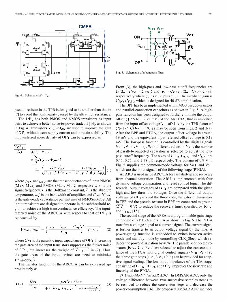
Fig. 5. Schematic of a bandpass filter.
From (3), the high-pass and low-pass cutoff frequencies areand ,
respectively where is plus . The mid-band gain is, which is designed for 40-dB amplification.
The BPF has been implemented with PMOS pseudo-resistorsand parallel-connection capacitors as shown in Fig. 5. A high-pass function has been designed to further eliminate the outputoffset ( 2.5 to 2.75 mV) of the ARCCIA, that is amplifiedfrom the input offset voltage of by the TPR factor of
as may be seen from Figs. 2 and 3(a).After the BPF and PTGA, the output offset voltage is around19 mV and the equivalent input referred offset voltage is 0.19mV. The low-pass function is controlled by the digital signals
. With different values of , the numberof parallel-connected capacitors is selected to adjust the low-pass cutoff frequency. The sizes of , and are0.45, 0.75, and 2.78 pF, respectively. The voltage of 0.9 V inFig. 5 supplies the common-mode voltage for Vo and Vowhich are the input signals of the following stage (PTGA).An ARU is used in the ARCCIA for fast start-up and recovery
from channel saturation. The ARU is implemented with fourdynamic voltage comparators and reset control logic. The dif-ferential output voltages of are compared with the givenhigh and low threshold voltages. Once the differential outputvoltages of exceed the thresholds, the gates of transistorsin TPR and the pseudo-resistor in BPF are connected to ground
0 V to reduce the recovery time, specified byand [15].The second stage of the AFEA is a programmable-gain stage
composed of a PTGA and a TIA as shown is Fig. 6. The PTGAtransfers a voltage signal to a current signal. The current signalis further transfer to an output voltage signal by the TIA. Apower-gating function is embedded to switch between activemode and standby mode by controlling CLK_Sleep which re-duces the power dissipation by 40%. The parallel-connected re-sistors are selected to adjust the transconduc-tance of the PTGA with digital control signals sothat three gain steps (1 , 3 , 10 ) can be provided for adap-tive signal scaling. The low input impedance of the TIA stage,consisting of , and , improves the slew rate andlinearity of the PTGA.2) Delta-Modulated SAR ADC: In DMSAR ADC, only the
voltage difference between two successive samples needs tobe resolved to reduce the conversion steps and decrease thepower consumption [16]. The proposed DMSAR ADC includes

236 IEEE JOURNAL OF SOLID-STATE CIRCUITS, VOL. 49, NO. 1, JANUARY 2014
Fig. 6. Schematic of PTGA and TIA.
Fig. 7. Architecture of the DMSAR ADC.
a switched-capacitor array, a time-shared comparator, a memoryarray, registers, an adder, and an asynchronous clock generatoras shown in Fig. 7. It is operated in three phases. First, a bi-nary-weighted DAC samples the value stored in the memoryarray for channel and output of AFEA to obtain the voltagedifference. Second, the coarse ADC determines the range of thesampled voltage difference. Finally, the fine ADC resolves thevoltage difference for LSBs. The comparator is shared in thecoarse and fine conversion phases. The 10-bit memory for eachchannel is required to store previously quantized data which aresent back to the DAC to obtain the signal difference for conver-sion from the same channel. Delta modulation is embedded inthe conversion process.In the proposed acquisition unit, one DMSAR ADC is shared
by eight AFEAs. The sampling rate is set to 62.5 kHz perchannel, which is sufficient for neural signal sampling. ForiEEG with 200-Hz bandwidth, 312 points are sampled withinone period for real-time observation. Since the signal differencebetween two consecutive samples is relatively smaller than thepeak signal swing, the delta modulation is adopted. As a result,the number of conversion steps can be further reduced, savingpower consumption by up to 66%.
Fig. 8. Architecture of a single-channel detector.
B. Bio-Signal Processor
The proposed BSP contains seizure detectors and one TXdata encoder for cyclic redundancy check (CRC). A power-ef-ficient fast Fourier transform (FFT) core, an approximated en-tropy (ApEn) encoder, and a linear least square (LLS) classi-fier are integrated as single seizure detector. The digitized iEEGsignals from the DMSAR ADC are sent to the BSP to extractthe features of the entropy and the spectrum. Fig. 8 shows theseizure detection algorithm and the signal processing flow. Bothsignal entropy and frequency spectrum are extracted as epilepticfeatures to enhance the seizure detection performance [17]. Inour previous studies [18]–[21], it was observed that ApEn withmultiband EEG power spectra can be used to effectively clas-sify seizure and nonseizure EEG signals.ApEn is a measure that evaluates the randomness or the
regularity of a time sequence [22]. An experiment showed thatthe ApEn index yielded a dominant factor (when comparedwith spectra analysis) in the trained LLS model for absenceseizure detection in [19]. In our LLS model, the weightingfactors of ApEn and two power spectrum bands are 51.6%,32%, and 16.4%, respectively. Multiband iEEG power spectraare therefore utilized as the complementary features of ApEn toreduce the false alarm rate and enhance the detection accuracy.Apart from the accuracy of the utilized algorithm on epilepticseizure, low computational cost, and short detection delayalso provides low power consumption and real-time ability forvarious implementations.Based on the algorithm presented in [19], a prototype with
enhanced 8051 microcontroller [21] is demonstrated to achieve117.66 mW/channel for the absence animal model. An im-provement in power consumption of over 10 is reported(7.21 mW/channel) on the implementation of high-performancereduced instruction set computing (RISC) processor [17] withcode optimization. To further improve energy efficiency, thefirst hardware-based prototype is presented in [20], whichprovides two-channel processing capability and is verified onfield-programmable gate array (FPGA). Through approxima-tion of numbers and pipeline execution, the detection accuracyand delay of hardware prototype still fail to meet specifications(accuracy % and delay second.) In this work, the SoCintegrates more channels of detectors [20] and achieves powerconsumption of 162.31 W/channel (77.91 J/detection.) The

CHEN et al.: FULLY INTEGRATED 8-CHANNEL CLOSED-LOOP NEURAL-PROSTHETIC CMOS SOC FOR REAL-TIME EPILEPTIC SEIZURE CONTROL 237
Fig. 9. Architecture of adaptive high-voltage-tolerant stimulator.
proposed BSP detects more than 92% of seizures within 0.8 s.It outperforms the support vector machine (SVD)-based EEGacquisition processor in [7], which achieves 84.4% detectionaccuracy within 2 s. It also provides the faster response thanprior works [23], [24].A two-phase seizure detection [18], [25], consisting of pa-
tient-specific training and online detection, is performed. Theutilized linear least-square model finds a best fitting curve tominimize mean-square errors between detection results (circuit)and desired output (determined by neurologist). In the off-linetraining stage, continuous neural signals of seizures (SWD) andnon-seizures (WK, SWS, and artifact) are recorded for featureextraction. iEEG data corresponding to various behavioral statesare utilized for training a classifier. The time-domain and fre-quency-domain characteristics of iEEG signals, with respect tovarious physiological states, are integrated as seizure detectionfeatures. These spontaneous events are used to train the seizureclassifier program off-line. The training procedure is performeduntil the accuracy is over 90% and detection delay is shorterthan 1.0 s.A short-range radio-frequency (RF) transmitter is integrated
into the SoC to provide real-time waveform observation. Beforewireless transmission, iEEG data packet is down-sampled by afactor of 4 to save data bandwidth. Next, the CRC encoder withCRC-7 polynomials is utilized against data corruption. A uni-versal asynchronous receiver/transmitter (UART)-like protocolis adopted to encapsulate iEEG data and CRC codes. CRC com-putation and wireless transmission are operated under 8 sam-pling clock. Incorporated with 8 sampling clock and down-sampling scheme, the iEEG data can be transmitted continu-ously for real-time monitoring.
C. Adaptive High-Voltage-Tolerant Stimulator
For system integration, a high-voltage-tolerant stimulatorwith adaptive loading in a standard process is proposed inorder to avoid the use of high-voltage transistors. The pro-posed stimulator consists of a high-voltage generator, a pair ofhigh-voltage-tolerant output drivers, and a pair of current con-trollers, as shown in Fig. 9. The stimulator has been designed todeliver biphasic stimulus currents with H-bridge topology [26].The biphasic stimulus pattern a constant A current. With
Fig. 10. Architecture of high-voltage generator.
a supply voltage 1.8 V, the biphasic stimulus currentsare modulated by a pair of enable signals andgenerated from the BSP. To adapt to a wide range of loadingimpedances between the electrode and the brain tissue, thehigh-voltage generator is designed to supply a variable voltage( , up to 10 V) for the output drivers.When the stimulator is activated, the enable signal
controls an anodic (cathodic) high-voltage-tolerantoutput driver to deliver anodic (cathodic) stimulus currents tothe electrode and brain tissue. The anodic (cathodic) currentcontroller detects the anodic (cathodic) stimulus current, andsends a control signal back to the high-voltage generator. Thehigh-voltage generator then delivers to the output drivers.The detailed circuits of each block for the loading impedanceof 10–250 k will be discussed in the following.High-Voltage Generator: As shown in Fig. 10, the
high-voltage generator consists of a five-stage charge pump,a voltage divider ( and ), a comparator, a PFM, a ringoscillator, a frequency divider, a two-phase clock generator, andtapped buffer. Because of the wide voltage range of , thehigh-voltage generator must be carefully designed. The chargepump circuit is adopted without sacrificing the gate–oxidereliability [27]. The output voltage of the five-stage chargepump circuit with 1.8 V supply can be pumped up toaround 10 V. To support such a wide range of voltages, thepumping frequency of the charge pump is adjustable. The PFMis proposed to choose and modulate the clock frequency. In thiswork, if is lower than 5 V, the PFM chooses a low-fre-quency clkd (3.125 MHz) as the central frequency. Otherwise,a high-frequency clks (31.25 MHz) is chosen. Using the lowerclock frequency helps to reduce the glitch current with thelower . If a higher or lower is required, the PFM alsomodulates the clock frequency to be higher or lower.The power efficiency of the charge pump is defined as
(4)
where and denote the loading current and the totalcurrent consumption in the charge pump [28]. Considering thefive-stage charge pump, the output voltage is
(5)

238 IEEE JOURNAL OF SOLID-STATE CIRCUITS, VOL. 49, NO. 1, JANUARY 2014
Fig. 11. Architecture of high-voltage-tolerant output driver and current con-troller with the parasitic diodes string in the output series transistors.
and the total current consumption is
(6)
where and denote the clock frequency, stage capaci-tance, and parasitic capacitance, respectively. Since this chargepump is designed to output a wide range of voltages,the clock frequency, total current, and power efficiency of thecharge pump vary with the output voltage. The simulated powerefficiency of the charge pump lies between 43% and 72%.High-Voltage-Tolerant Output Driver: Fig. 11 shows the an-
odic and cathodic high-voltage-tolerant output drivers. It in-cludes associated parasitic-diode string in the output series tran-sistors, which consist of a level shifter, a pre-driver, and stacked3.3-V MOS transistors. The stacked MOS structure along with3.3-V transistors placed between and ground can sustainup to 10 V without electrical overstress issues [29].The level shifter is designed to convert the low (0 V/1.8 V)
enable signals to a high-voltage level. The pre-driver receivesthe high-voltage signal and then controls the output stage ofstacked transistors. The pre-driver outputs are varied accordingto the loading impedance. The PMOS and NMOS transistors inoutput stage are well controlled to decide whether the stimula-tion is on. For example, if the loading impedance leads the stim-ulus voltage to 4.3 V/9.2 V, the pre-driver outputs forM –Mare 0 V/0 V, 1.4 V/3.3 V, 2.9 V/6.3 V, 2.9 V/6.3 V, 2.9 V/6.3 V,and 2.9 V/6.5 V, respectively. All voltage differences acrossthe stacked MOS transistors are smaller than 3.3 V to sustainreliability.Current Controller: The current controller consists of a
current mirror, a trimmable resistor , and a comparator.When the stimulator is turned on, the stimulus current flowsthrough both stacked transistors and current mirror to inducea proportional current (I ). The current controller uti-lizes the I flowing through to generate a voltagesignal to compare with a referencevoltage . Our previous studies have demonstrated anintra-incertal current stimulation of 30 A to successfullystop seizures [19], [21], [30]. The comparator compares thesetwo voltages and determines if the stimulus current is underor below 30 A. The adjustable supply voltage forthe output driver is controlled by the output signal of the
Fig. 12. Architecture of the OOK MedRadio-band transceiver.
current controller. If the anodic stimulus current is lowerthan 30 A, the output signal of the current controller goeshigh 1.8 V . The high-voltage generator keepspumping to provide a higher voltage until the anodic stimuluscurrent reaches 30 A. Once the anodic stimulus current ishigher than 30 A, the output of the current controller goeslow 0 V . The high-voltage generator will stoppumping until the anodic stimulus current returns to 30 A.Since the stimulus current is 30 A per channel, the powerconsumption of the current mirror in the current controller isabout 10 W. The latency from the input to the output of thecurrent controller is around 25 ns. The feedback control loopcauses the anodic stimulus current to keep around 30 A duringanodic stimulation. Similarly, the cathodic stimulus current iskept at 30 A during cathodic stimulation.
D. MedRadio-Band Transceiver
To reduce power dissipation and to minimize chip area forimplantable devices, OOK modulation has been adopted fordata transmission. The proposed OOK transceiver is designedfor the FCC MedRadio Service band (401–406 MHz). It in-cludes a transmitter (TX), a T/R switch, and a receiver, as shownin Fig. 12. The transmitter (TX) is composed of a ring-oscil-lator VCO with an OOK function generator [31]. The receiver(RX) has a single-ended-to-differential amplifier (SDA), fourcascaded fully differential amplifiers (FDAs), and a full-wavecurrent-mode envelope detector (demodulator) [32] The pro-posed detector rectifies the input signal with appropriate gain toeliminate extra baseband amplifier. Local oscillator and down-conversion mixer are not included to reduce power consump-tion and chip area. The demodulator is designed to recover theamplified signals from the gain stages with a bandwidth of upto 4 MHz. A T/R switch is designed to increase the isolationand switch between TX and RX ports. The output power of thetransmitter is 17 dBm, which is lower than the specified limi-tation of 16 dBm. At the receiver, the sensitivity is 53 dBmat a distance of 10 cm.
E. Inductive Link Power Supply System
In order to eliminate the use of a battery to avoid frequentsurgery for battery replacement, an inductive link power trans-mission system is proposed to supply the power for the SoC.The architecture of the proposed inductive link power supplysystem consists of a pair of near-field coils, an active rectifier,and three local LDOs, as shown in Fig. 13. The primary coiltransmits the power through a magnetic inductive link at a car-rier frequency of 13.56 MHz in the Industrial, Scientific and

CHEN et al.: FULLY INTEGRATED 8-CHANNEL CLOSED-LOOP NEURAL-PROSTHETIC CMOS SOC FOR REAL-TIME EPILEPTIC SEIZURE CONTROL 239
Fig. 13. Architecture of the inductive link power supply system.
Fig. 14. Schematic of the active rectifier.
Medical (ISM) band to the secondary coil. The rectifier con-verts the received ac power to a dc signal . The LDOsregulate to support stable power sources for different cir-cuit requirements. In the proposed rectifier, a fully on-chip dy-namic compensated topology is employed to enhance the powerefficiency. The multi-LDO topology is adopted to optimize theLDO performance and isolate the disturbances from digital cir-cuit domain.Active Rectifier: The schematic of the active rectifier is
shown in Fig. 14 The power PMOSs (M , M ) form across-coupled pair and function as switches [33], which areturned on by . Two two-terminal comparators cmp1 andcmp2 are used to control the gate voltages of the power NMOSs(M , M ) by comparing the input node voltages (V andV ) with ground voltage respectively. A start-up circuit con-trols the comparator output voltage when starts from zero.The voltage limiter limits to a maximum value of 2.5 V(normally at 2 V) when the input power of the active rectifieris too large. The output voltages and from thecomparators of cmp1 and cmp2, respectively, are used todynamically adjust the current sources of the differential inputpairs. With different bias currents, different input offsetvoltages are created to compensate both turn-on and turn-offgate delay times of the power MOS devices to achieve anefficiency of 84.8%, with 20-mA output current and 327.5-mVdropout voltage.Low-Dropout Regulator: A topology of multiple local capac-
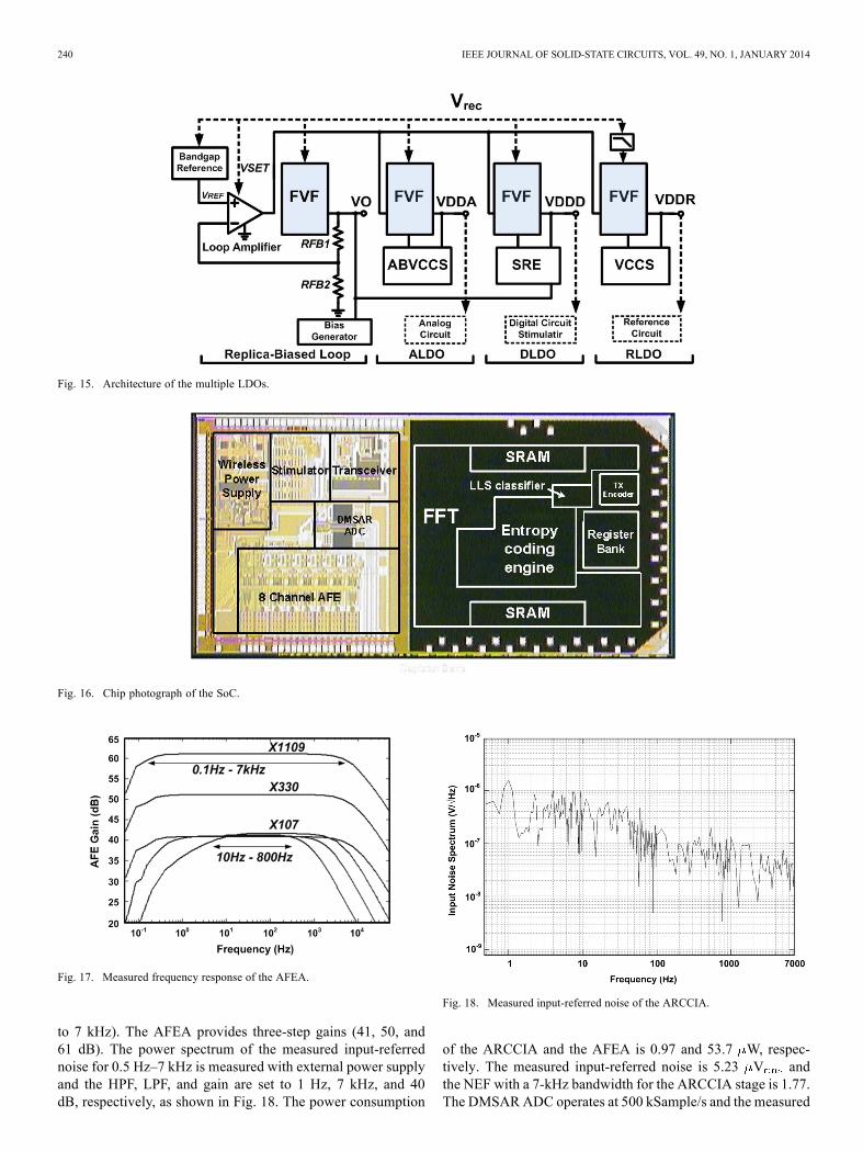
itor-free LDOs with a replica-biased loop is proposed to isolatethe interference between power domains and satisfy differentcircuit requirements, as shown in Fig. 15. The output stage ofeach LDO is the same but with different compensation tech-niques according to the requirements in driving capabilities.
Each regulation loop is designed for each power domain andit drives the designated circuit individually.ALDO, RLDO, and DLDO are designed for analog circuits,
reference voltages, and BSP with stimulator circuits, respec-tively. The replica-biased loop is used to generate a stable biasvoltage for load regulation whereas the fast voltage reg-ulation is achieved by the local regulation loops. VO, VDDA,VDDR, VDDD are the output voltages of replica-biased loop,ALDO, RLDO, and DLDO, respectively. Flipped voltage fol-lower (FVF) [34] cells are used as the output stages for theLDOs. The adaptive-biased voltage-controlled current source(ABVCCS) and voltage control current source (VCCS) are de-signed to enhance the stability under a variety of load conditionsfor ALDO and RLDO. A slew-rate enhancement (SRE) circuitis used to achieve fast transient response in the absence of alarge external capacitor for DLDO.
IV. EXPERIMENTAL RESULTS
Fig. 16 shows the chip photograph. The proposed SoC wasfabricated in an 0.18- m CMOS process and the total chip areais 13.47 mm including the ESD pads. Each subsystem wastested separately and the function of the whole system was ver-ified in an animal experiment.
A. System Verification
Fig. 17 shows the measured frequency response of the AFEAwhere both the high-pass and low-pass cut-off frequencies aretunable. The high-pass cut-off frequency of the AFEA is mea-sured by adjusting the gate voltage of the pseudo-resistor(M ,M ) in Fig. 5 to eliminate the EDOwhile maintainthe signal amplitude of the low-frequency signal. The high-pass(low-pass) cut-off frequency is adjusted from 0.1 to 10 Hz (0.8
240 IEEE JOURNAL OF SOLID-STATE CIRCUITS, VOL. 49, NO. 1, JANUARY 2014
Fig. 15. Architecture of the multiple LDOs.
Fig. 16. Chip photograph of the SoC.
Fig. 17. Measured frequency response of the AFEA.
to 7 kHz). The AFEA provides three-step gains (41, 50, and61 dB). The power spectrum of the measured input-referrednoise for 0.5 Hz–7 kHz is measured with external power supplyand the HPF, LPF, and gain are set to 1 Hz, 7 kHz, and 40dB, respectively, as shown in Fig. 18. The power consumption
Fig. 18. Measured input-referred noise of the ARCCIA.
of the ARCCIA and the AFEA is 0.97 and 53.7 W, respec-tively. The measured input-referred noise is 5.23 V andthe NEF with a 7-kHz bandwidth for the ARCCIA stage is 1.77.The DMSARADC operates at 500 kSample/s and the measured

CHEN et al.: FULLY INTEGRATED 8-CHANNEL CLOSED-LOOP NEURAL-PROSTHETIC CMOS SOC FOR REAL-TIME EPILEPTIC SEIZURE CONTROL 241
Fig. 19. (a) Measured stimulus currents with different loading impedances. (b) Measured stimulus currents under different loading impedance. (c) Measuredunder different loading impedance. (d) Measured power consumption under different loading impedance.
ENOB is 9.57 b with power of 3.0 W per channel. The mea-sured INL/DNL of the DMSAR ADC is 0.32/0.08 LSB.Fig. 19(a) shows the measured stimulus currents passing
through the loading impedance. A 250 k resistor and a4 nF/200 nF capacitor are used to represent the electrodeand brain tissue. The measured stimulus current, , andtotal power for various loading impedances are shown inFig. 19(b)-(d). As can be seen from Fig. 19, the stimuluscurrent is limited within 30–35 A. The proposed stimulatorcan be operated at a lower operating voltage and consumes lesspower for lower loading impedances.The MedRadio-band transceiver was tested at a data rate of
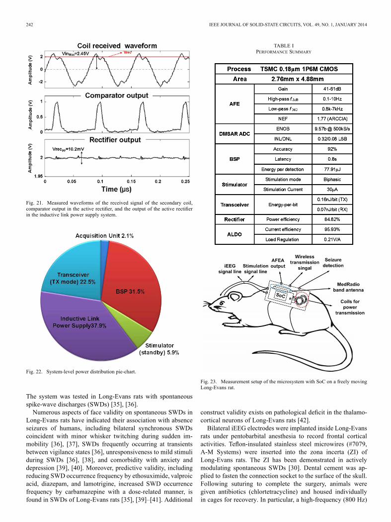
4 Mbps through the 401–406-MHz band. Fig. 20 shows thetransmitted packet to the TX port, the modulated OOK signalreceived at the RX port, and the recovered signal from the RX.From Fig. 20, the encoded OOK signal is transmitted and recov-ered to the original signal at RX. The output power of the TXis 17.2 dBm and the sensitivity is 45.7 dBm. With a datarate of 4 Mbps, the energy-per-bit of the TX and RX is 0.16 and0.07 nJ/b, respectively.Fig. 21 shows the received waveform of the secondary coil,
comparator output in the active rectifier, and the output of theactive rectifier in the inductive link power supply system. Theamplitude of the signal received by the receiver coil is 2.45 V.After being rectified, the output DC voltage becomes 2 V with10.2 mV ripples. The LDOs regulate the noisy voltage to sustaina steady voltage of 1.8 V with 5.9/72.4/1.4 mV in ALDO/DLDO/RLDO regions.The power consumption of the proposed SoC is 2.8 mW, and
the system-level power breakdown is shown as Fig. 22. The chipperformance is summarized in Table I.
Fig. 20. Measured waveforms of the transmitted packet signal to the TX, thereceived signal at RX, and the recovered signal.
B. Animal Experiment
Four adult Long-Evans rats were tested in this study. All sur-gical and experimental procedures were reviewed and approvedby the Institutional Animal Care and Use Committee of Na-tional Cheng Kung University, and all experiments comply withNIH (USA) recommended guidelines on the ethical use of ani-mals. Based on the system verification results, the SoC is usedin a microsystem setup and applied to the animal experiment.
242 IEEE JOURNAL OF SOLID-STATE CIRCUITS, VOL. 49, NO. 1, JANUARY 2014
Fig. 21. Measured waveforms of the received signal of the secondary coil,comparator output in the active rectifier, and the output of the active rectifierin the inductive link power supply system.
Fig. 22. System-level power distribution pie-chart.
The system was tested in Long-Evans rats with spontaneousspike-wave discharges (SWDs) [35], [36].Numerous aspects of face validity on spontaneous SWDs in
Long-Evans rats have indicated their association with absenceseizures of humans, including bilateral synchronous SWDscoincident with minor whisker twitching during sudden im-mobility [36], [37], SWDs frequently occurring at transientsbetween vigilance states [36], unresponsiveness to mild stimuliduring SWDs [36], [38], and comorbidity with anxiety anddepression [39], [40]. Moreover, predictive validity, includingreducing SWD occurrence frequency by ethosuximide, valproicacid, diazepam, and lamotrigine, increased SWD occurrencefrequency by carbamazepine with a dose-related manner, isfound in SWDs of Long-Evans rats [35], [39]–[41]. Additional
TABLE IPERFORMANCE SUMMARY
Fig. 23. Measurement setup of the microsystem with SoC on a freely movingLong-Evans rat.
construct validity exists on pathological deficit in the thalamo-cortical neurons of Long-Evans rats [42].Bilateral iEEG electrodes were implanted inside Long-Evans
rats under pentobarbital anesthesia to record frontal corticalactivities. Teflon-insulated stainless steel microwires (#7079,A-M Systems) were inserted into the zona incerta (ZI) ofLong-Evans rats. The ZI has been demonstrated in activelymodulating spontaneous SWDs [30]. Dental cement was ap-plied to fasten the connection socket to the surface of the skull.Following suturing to complete the surgery, animals weregiven antibiotics (chlortetracycline) and housed individuallyin cages for recovery. In particular, a high-frequency (800 Hz)
CHEN et al.: FULLY INTEGRATED 8-CHANNEL CLOSED-LOOP NEURAL-PROSTHETIC CMOS SOC FOR REAL-TIME EPILEPTIC SEIZURE CONTROL 243
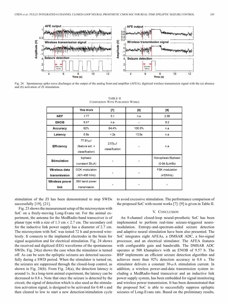
Fig. 24. Spontaneous spike-wave discharges at the output of the analog front-end amplifier (AFEA), digitized wireless transmission signal with the (a) absenceand (b) activation of ZI stimulation.
TABLE IICOMPARISON WITH PUBLISHED WORKS
stimulation of the ZI has been demonstrated to stop SWDssuccessfully [19], [21].Fig. 23 shows themeasurement setup of themicrosystemwith
SoC on a freely-moving Long-Evans rat. For the animal ex-periment, the antenna for the MedRadio-band transceiver is ofplanar type with a size of 1.3 cm 2.7 cm. The secondary coilfor the inductive link power supply has a diameter of 2.7 cm.The microsystem with SoC was tested 72 h and powered wire-lessly. It connects to the implanted electrodes in the brain forsignal acquisition and for electrical stimulation. Fig. 24 showsthe received and digitized iEEG waveforms of the spontaneousSWDs. Fig. 24(a) shows the case when the stimulator is turnedoff. As can be seen the epileptic seizures are detected success-fully during a SWD period. When the stimulator is turned on,the seizures are suppressed through the closed-loop control, asshown in Fig. 24(b). From Fig. 24(a), the detection latency isaround 1s. In a long-term animal experiment, the latency can bedecreased to 0.8 s. Note that once the seizure is detected by thecircuit, the signal of detection which is also used as the stimula-tion activation signal, is designed to be activated for 0.48 s andthen cleared to low to start a new detection/stimulation cycle
to avoid excessive stimulation. The performance comparison ofthe proposed SoC with recent works [7]–[9] is given in Table II.
V. CONCLUSION
An 8-channel closed-loop neural-prosthetic SoC has beenimplemented to perform real-time seizure-triggered neuro-modulation. Entropy-and-spectrum-aided seizure detectionand adaptive neural stimulation have been also presented. TheSoC integrates eight AFEAs, a DMSAR ADC, a bio-signalprocessor, and an electrical stimulator. The AFEA featureswith configurable gain and bandwidth. The DMSAR ADCoperates at 500 kSamples/s with an ENOB of 9.57 b. TheBSP implements an efficient seizure detection algorithm andachieves more than 92% detection accuracy in 0.8 s. Thestimulator delivers a constant 30- A stimulation current. Inaddition, a wireless power-and-data transmission system in-cluding a MedRadio-band transceiver and an inductive linkpower supply system, has been embedded for signal monitoringand wireless power transmission. It has been demonstrated thatthe proposed SoC is able to successfully suppress epilepticseizures of Long-Evans rats. Based on the preliminary results,

244 IEEE JOURNAL OF SOLID-STATE CIRCUITS, VOL. 49, NO. 1, JANUARY 2014
the developed closed-loop seizure control SoC is a promisingsolution for treating epilepsy. For future applications on humanimplants, the chip package, antenna, and coils will be carefullydesigned to meet all of the system performance and regulatoryrequirements.
ACKNOWLEDGMENT
The authors would like to thank National Chip Implementa-tion Center for chip design environment support.
REFERENCES
[1] P. Kwan, S. C. Schachter, and M. J. Brodie, “Current concepts: Drug-resistant epilepsy,” N. Engl. J. Med., vol. 365, no. 10, pp. 919–926,Sep. 2011.
[2] E. F. Chang and N. M. Barbaro, “Epilepsy surgery: The emerging fieldof neuromodulation,”Neurosurg Clin N. Amer., vol. 22, no. 4, pp. ix–x,Oct. 2011.
[3] F. A. Al-Otaibi, C. Hamani, and A. M. Lozano, “Neuromodulation inepilepsy,” Neurosurgery, vol. 69, no. 4, pp. 957–979, Oct. 2011.
[4] P. R. Gigante and R. R. Goodman, “Responsive neuromodulation forthe treatment of epilepsy,” Neurosurg Clin N. Amer., vol. 22, no. 4, pp.477–480, Oct. 2011.
[5] J. C. LaManna, K. A. McCracken, M. Patil, and O. J. Prohaska, “Stim-ulus-activated changes in brain tissue temperature in the anesthetizedrat,” Metabolic Brain Disease, vol. 4, pp. 225–237, 1989.
[6] S. Kim, P. Tathireddy, R. A. Normann, and F. Solzbacher, “Thermalimpact of an active 3-D microelectrode array implanted in the brain,”IEEE Trans. Neural Syst. Rehabil. Eng., vol. 15, no. 4, pp. 493–501,Dec. 2007.
[7] J. Yoo, L. Yan, D. E. Damak, M. A. B. Altaf, A. H. Shoeb, and A.P. Chandrakasan, “An 8-channel scalable EEG acquisition SoC withpatient-specific seizure classification and recording processor,” IEEEJ. Solid-State Circuits, vol. 48, no. 1, pp. 214–228, Jan. 2013.
[8] M. Salam, M. Sawan, and D. Nguyen, “A novel low-power-im-plantable epileptic seizure-onset detector,” IEEE Trans. Biomed.Circuits Syst., vol. 5, no. 6, pp. 568–578, Dec. 2011.
[9] M. Azin, D. Guggenmos, S. Barbay, R. Nudo, and P. Mohseni, “A bat-tery-powered activity-dependent intracortical microstimulation ic forbrain-machine-brain interface,” IEEE J. Solid-State Circuits, vol. 46,no. 4, pp. 731–745, Apr. 2011.
[10] W.-M. Chen, H. Chiueh, T.-J. Chen, C.-L. Ho, C. Jeng, S.-T. Chang,M.-D. Ker, C.-Y. Lin, Y.-C. Huang, T.-Y. Fan, M.-S. Cheng, C.-W.Chou, S.-F. Liang, T.-C. Chien, S.-Y. Wu, Y.-L. Wang, F.-Z. Shaw,Y.-H. Huang, C.-H. Yang, J.-C. Chiou, C.-W. Chang, L.-C. Chou, andC.-Y. Wu, “A fully integrated 8-channel closed-loop neural-prostheticSoC for real-time epileptic seizure control,” in IEEE Int. Solid-StateCircuits Conf. Dig. Tech. Papers, Feb. 2013, pp. 286–287.
[11] A. A. Boulton, G. B. Baker, and C. H. Vanderwolf, NeurophysiologicalTechniques: II. Applications to Neural Systems. Berlin, Germany:Springer, 1990.
[12] E. Leuthardt, G. Schalk, J. Wolpaw, J. Ojemann, and D. Moran,“A brain-computer interface using electrocorticographic signals inhuman,” J. Nerual Eng., vol. 1, no. 2, pp. 63–71, 2004.
[13] R. R. Harrison and C. Charles, “A low-power low-noise CMOS am-plifier for neural recording applications,” IEEE J. Solid-State Circuits,vol. 38, no. 6, pp. 958–965, Jun. 2003.
[14] X. Zou, W. S. Liew, L. Yao, and Y. Libin, “A 1 V 22 uW 32-channelimplantable EEG recording IC,” in IEEE Int. Solid-State Circuits Conf.Dig. Tech. Papers, Feb. 2010, pp. 126–127.
[15] F. Heer, S. Hafizovic, W. Franks, A. Blau, C. Ziegler, and A. Hierle-mann, “CMOS microelectrode array for bidirectional interaction withneuronal networks,” IEEE J. Solid-State Circuit, vol. 41, no. 7, pp.1620–1629, Jul. 2006.
[16] Y.-F. Lyu, C.-Y. Wu, L.-C. Liu, andW.-M. Chen, “A low power 10 Bit500 kS/s delta-modulated SAR ADC (DMSAR ADC) for implantablemedical devices,” in Proc. IEEE Int. Symp. Circuits Syst., May 2013,pp. 2046–2049.
[17] T.-J. Chen, H. Chiueh, S.-F. Liang, S.-T. Chang, C. Jeng, Y.-C. Hsu,and T.-C. Chien, “The implementation of a low-power biomedicalsignal processor for real-time epileptic seizure detection on absenceanimal models,” IEEE J. Emerg. Sel. Topic Circuits Syst., vol. 1, no.4, pp. 613–621, Dec. 2011.
[18] S. Liang, H. Wang, and W. Chang, “Combination of EEG complexityand spectral analysis for epilepsy diagnosis and seizure detection,”EURASIP J. Adv. Signal Process., vol. 2010, pp. 1–15, 2010.
[19] S.-F. Liang, Y.-C. Liao, F.-Z. Shaw, D. W. Chang, C. P. Young, andH. Chiueh, “Closed-loop seizure control on epileptic rat models,” J.Neural Eng., vol. 8, no. 4, p. 045001, 2011.
[20] T.-J. Chen, C. J. , S.-T. Chang, H. Chiueh, S.-F. Liang, Y.-C. Hsu, andT.-C. Chien, “A hardware implementation of real-time epileptic seizuredetector on FPGA,” in Proc. IEEE Biomed. Circuits Syst. Conf., Nov.2011, pp. 25–28.
[21] C.-P. Young, S.-F. Liang, D.-W. Chang, Y.-C. Liao, F.-Z. Shaw, andC.-H. Hsieh, “A portable wireless online closed-loop seizure controllerin freely moving rats,” IEEE Trans. Instrum. Meas., vol. 60, no. 2, pp.513–521, Feb. 2011.
[22] S. M. Pincus, “Approximate entropy as a measure of system com-plexity,” Natl. Acad. Sci. USA, vol. 88, no. 6, pp. 2297–301, 1991.
[23] M. Altaf, J. Tillak, Y. Kifle, and J. Yoo, “A 1.83 J/classification non-linear support-vector-machine-based patient-specific seizure classifi-cation SoC,” in IEEE Int. Solid-State Circuits Conf. Dig. Tech. Papers,Feb. 2013, pp. 100–101.
[24] N. Verma, A. Shoeb, J. Bohorquez, J. Dawson, J. Guttag, and A. P.Chandrakasan, “A micro-power EEG acquisition SoC with integratedfeature extraction processsor for chronic seizure detection system,”IEEE J. Solid-State Circuits, vol. 45, no. 4, pp. 804–816, Jan. 2010.
[25] S. Liang, W. Chang, and H. Chiueh, “EEG-based absence seizure de-tection methods,” in Proc. Int. Joint Conf. Neural Networks, July 2010,pp. 1–4.
[26] M. Sawan, F. Mounaim, and G. Lesbros, “Wireless monitoring of elec-trode-tissues interfaces for long term characterization,” Analog Integr.Circuits Signal Process., vol. 55, no. 1, pp. 103–114, Apr. 2008.
[27] M.-D. Ker, S.-L. Chen, and C.-S. Tsai, “Design of charge pump cir-cuit with consideration of gate oxide reliability in low-voltage CMOSprocess,” IEEE J. Solid-State Circuits, vol. 41, no. 5, pp. 1100–1107,May 2006.
[28] G. Palumbo, D. Pappalardo, and M. Gaibotti, “Charge-pump circuits:power-consumption optimization,” IEEE Trans. Circuits Syst. I,Fundam. Appl. Theory, vol. 49, no. 11, pp. 1535–1542, Nov. 2002.
[29] C. Wang, C. Hsu, and Y. Liu, “A 1/2 VDD to 3 VDD bidirectionalI/O buffer with a dynamic gate bias generator,” IEEE Trans. CircuitsSyst. I, Reg. Papers, vol. 57, no. 7, pp. 1642–1653, Jul. 2010.
[30] F.-Z. Shaw, Y.-F. Liao, R.-F. Chen, Y.-H. Huang, and R. C. S. Lin,“The zona incerta modulates spontaneous spike-wave discharges in therat,” J. Neurophysiol., vol. 109, no. 10, pp. 2505–2516, 2013.
[31] L.-C. Liu, M.-H. Ho, and C.-Y. Wu, “A medradio-band low-energy-per-bit CMOS OOK transceiver for implantable medical devices,” inProc. Biomed. Circuits Syst. Conf., Nov. 2011, pp. 153–156.
[32] C.-W. Chou, L.-C. Liu, and C.-Y. Wu, “A MedRadio-band low-en-ergy-per-bit 4-Mbps CMOSOOK receiver for implantable medical de-vices,” in Proc. 35th Annu. Int. Conf. IEEE Eng. Med. Biol. Soc., Jul.2013, pp. 5171–5174.
[33] S. Guo and H. Lee, “An efficiency-enhanced CMOS rectifier with un-balanced-biased comparators for transcutaneous powered high-currentimplants,” IEEE J. Solid-State Circuits, vol. 44, no. 6, pp. 1796–1804,Jun. 2009.
[34] J. Ramirez-Angulo, R. G. Garvajal, A. Torralba, J. Galan, A. P. Veg-aLeal, and J. Tombs, “The flipped voltage follower: A useful cell forlow-voltage low-power circuit design,” in Proc. IEEE Int. Symp. Cir-cuits Syst., May 2002, vol. 3, pp. 615–618.
[35] F.-Z. Shaw, “7–12 Hz high-voltage rhythmic spike discharges in ratsevaluated by antiepileptic drugs and flicker stimulation,” J. Neuro-physiol., vol. 97, no. 1, pp. 238–247, 2007.
[36] F.-Z. Shaw, “Is spontaneous high-voltage rhythmic spike discharge inLong Evans rats an absence-like seizure activity?,” J. Neurophysiol.,vol. 91, no. 1, pp. 63–77, 2004.
[37] F.-Z. Shaw and Y.-F. Liao, “Relation between activities of the cortexand vibrissae muscle during high-voltage rhythmic spike discharges inrats,” J. Neurophysiol., vol. 93, no. 5, pp. 2435–2448, 2005.
[38] F.-Z. Shaw, S.-Y. Lee, and T.-H. Chiu, “Modulation of somatosensoryevoked potential during wake-sleep states and spike-wave discharge inthe rat,” Sleep, vol. 29, no. 3, pp. 285–293, 2006.
[39] H.-Y. Huang, H.-W. Lee, S.-D. Chen, and F.-Z. Shaw, “Lamotrigineameliorates seizures and psychiatric comorbidity in a rat modelof spontaneous absence epilepsy,” Epilepsia, vol. 53, no. 11, pp.2005–2014, 2012.
[40] F.-Z. Shaw, S.-H. Chuang, K.-R. Shieh, and Y.-J. Wang, “Depression-and anxiety-like behaviors of a rat model with absence epileptic dis-charges,” Neurosci., vol. 160, no. 2, pp. 382–393, 2009.

CHEN et al.: FULLY INTEGRATED 8-CHANNEL CLOSED-LOOP NEURAL-PROSTHETIC CMOS SOC FOR REAL-TIME EPILEPTIC SEIZURE CONTROL 245
[41] S.-D. Chen, K.-H. Yeh, Y.-H. Huang, and F.-Z. Shaw, “Effects of in-tracranial administration of ethosuximide in rats with spontaneous orpentylenetetrazol-induced spike-wave discharges,” Epilepsia, vol. 52,no. 7, pp. 1311–1318, 2011.
[42] P. O. Polack and S. Charpier, “Intracellular activity of cortical and tha-lamic neurons during high-voltage rhythmic spike discharge in Long-Evans rats in vivo,” J. Physiol., vol. 571, no. 2, pp. 461–476, 2006.
Wei-Ming Chen (M’12) received the M.S. andPh.D. degrees from the Institute of Electronics,National Chiao Tung University, Hsinchu, Taiwan,in 2005 and 2013, respectively.He is now a Postdoctoral Research Fellow with
Biomedical Electronics Translational ResearchCenter, National Chiao Tung University, Hsinchu,Taiwan. His major research interests are biomedicalelectronics and analog integrated circuits design.
Herming Chiueh (M’90) received the B.S. degree inelectrophysics from National Chiao Tung University,Hsinchu, Taiwan, and the M.S. and Ph.D. degrees inelectrical engineering from University of SouthernCalifornia, Los Angeles, CA, USA.From 1996 to 2002, he was with Information
Sciences Institute, University of Southern California,Marina del Rey, CA, USA. He has participated inthe VLSI effort on several large projects in USC/ISIand most recently participated the developmentof a 55-million transistor processing-in-memory
(PIM) chip. From 2009 to 2012, he has given more than 20 invited talksregarding his recent research in “closed-loop epileptic seizure detection”and “low-power sigma-delta data converters” in conferences and workshopsas well as difference campuses and research institutes. He currently servesas an Associate Professor with the Department of Electrical and ComputerEngineering, National Chiao Tung University, Hsinchu, Taiwan. His researchinterests include system-on-chip design methodology, low-power integratedcircuits, neural interface circuits, and biomimetic systems.Dr. Chiueh served as Demonstrations Chair on 2012 IEEE Biomedical
Circuits and Systems Conferences (BIOCAS 2012,) Conference Secretariat on2007 IEEE SOC Conference, and Finance Chair on 2007 IEEE InternationalWorkshop on Memory Technology, Design and Testing. He is a member ofTechnical Committee on “Biomedical Circuits and Systems” and “Nanoelec-tronicsGigascale System” in IEEE Circuits and Systems Society. He alsoserved as Education Affairs Officer in IEEE Circuits and Systems Society,Taipei Chapter in 2011. He was member of technical program committee andsession chair in several conferences, such as ISCAS, MWSCAS, THERMINIC,APSCAS, THETA, and ICECS.
Tsan-Jieh Chen (M’11) received the B.S. degree inelectrical engineering from the Ming Chi Universityof Technology, Taiwan, in 2007, and the Ph.D. degreein communication engineering from National ChiaoTung University, Hsinchu, Taiwan, in 2012.He is now a Postdoctoral Research Fellow with
the Biomedical Electronics Translational ResearchCenter, National Chiao Tung University, Hsinchu,Taiwan. His research interests include integratedchip design, low-power design methodology, andembedded systems for biomedical applications.
Chia-Lun Ho received the B.S. degree in electricalengineering from National Chiao Tung University,Hsinchu, Taiwan, in 2011, where he is currentlyworking toward the M.S. degree.
Chi Jeng received the B.S. degree in engineering sci-ence from National Cheng Kung University, Tainan,Taiwan, in 2009, and the M.S. degree in communica-tion engineering from National Chiao Tung Univer-sity, Hsinchu, Taiwan, in 2012.Since January 2012, she has been with Chunghwa
Telecom Laboratories, where she is an AssociateResearch Fellow and is involved in the designof various vehicular communication systems.Her current research interests include low-powersystem-on-chip design and intelligent transportation
system development.
Ming-Dou Ker (F’08) received the Ph.D. degreefrom the Institute of Electronics, National ChiaoTung University, Hsinchu, Taiwan, in 1993.He then became the Department Manager with the
VLSI Design Division, Computer and Communica-tion Research Laboratories, Industrial TechnologyResearch Institute (ITRI), Hsinchu, Taiwan. Since2004, he has been a Full Professor with the De-partment of Electronics Engineering, NationalChiao Tung University, Hsinchu, Taiwan. During2008–2011, he was rotated to be Chair Professor and
the Vice President of I-Shou University, Kaohsiung, Taiwan. Now, he has beenthe Distinguished Professor in the Department of Electronics Engineering,National Chiao-Tung University (NCTU), Taiwan; as well as the Dean ofCollege of Photonics, NCTU. He even served as the Executive Director ofNational Science and Technology Program on System-on-Chip (NSoC) inTaiwan during 2010–2011 and is currently serving as the Executive Directorof National Science and Technology Program on Nano Technology (NPNT)in Taiwan (2011–2014). In the technical field of reliability and quality designfor microelectronic circuits and systems, he has published over 480 technicalpapers in international journals and conferences. He has proposed many solu-tions to improve the reliability and quality of integrated circuits, which havebeen granted with hundreds of U.S. patents and Taiwan patents. He had beeninvited to teach and/or to consult the reliability and quality design for integratedcircuits by hundreds of design houses and semiconductor companies in theworldwide IC industry. His current research interests include reliability andquality design for nanoelectronics and gigascale systems, circuits and systemsfor information displays, as well as the circuits and systems for biomedicalapplications.Prof. Ker has served as member of the Technical Program Committee and the
Session Chair of numerous international conferences for many years. He everserved as the Associate Editor for the IEEE TRANSACTIONS ON VERY LARGE-SCALE INTEGRATION (VLSI) SYSTEMS during 2006–2007. He was selected as aDistinguished Lecturer of the IEEE Circuits and Systems Society (2006–2007)and the IEEE Electron Devices Society (2008–2013). He was the FoundingPresident of Taiwan ESDAssociation. Starting in 2012, he is currently served asthe editor of IEEE TRANSACTIONS ON DEVICE AND MATERIALS RELIABILITY.

246 IEEE JOURNAL OF SOLID-STATE CIRCUITS, VOL. 49, NO. 1, JANUARY 2014
Chun-YuLin (M’09) received the Ph.D. degree fromthe Institute of Electronics, National Chiao TungUni-versity, Hsinchu, Taiwan, in 2009.He is currently the Assistant Professor with the
Department of Applied Electronics Technology, Na-tional Taiwan Normal University, Taiwan, and alsothe Secretary-General of Taiwan ESD Association.His current research interests include ESD protectiondesigns and biomimetic circuit designs.
Ya-Chun Huang received the B.S. and M.S. degreesfrom National Chiao Tung University, Hsinchu,Hsinchu, Taiwan, in 2010 and 2012, respectively.
Chia-Wei Chou received the B.S. degree fromthe Department of Electrical Engineering, NationalChung Hsing University, Taichung, Taiwan, in 2010,and the M.S. degree from the Institute of Electronics,National Chiao Tung University, Hsinchu, Taiwan,in 2012.
Tsun-Yuan Fan received the B.S. degree from theDepartment of Electronics Engineering, NationalChiao Tung University, Chiay, Taiwan, in 2010, andthe M.S. degree from the Institute of Electronics,National Chiao Tung University, Hsinchu, Taiwan,in 2012.
Ming-Seng Cheng received the B.S. degree fromthe Department of Electrical Engineering, NationalChung Cheng University, Chiay, Taiwan, in 2010,and the M.S. degree from the Institute of Electronics,National Chiao Tung University, Hsinchu, Taiwan,in 2012.
Yue-Loong Hsin received the M.D. degree fromKaohsiung Medical University, Kaohsiung, Taiwan.In 1998, he finished his residency training of neu-
rology and was qualified as a neurology specialist.Since then, he visited the Department of BrainPathophysiology at Kyoto University in 1999, wherehe focused on the treatment of epilepsy clinicallyand neurophysiology research about epilepsy. Hethen became a Member of the Neuroscience Centerat Hualien Tz Chi Hospital, where the first epilepsysurgery was conducted in 2000. In 1999, he began to
collaborate with engineers to develop algorithms for automated temporospatialdetection of seizure onset and therapeutic device. Through this effort, his clin-ical and basic researches about the pathophysiology of epilepsy and analysisof neuroimaging are also in progress. Currently, he is the head of NeurologicDepartment at Chung Shan Medical University Hospital.
Sheng-Fu Liang (M’09) received the B.S. and M.S.degrees in control engineering and Ph.D. degreein electrical and control engineering from NationalChiao Tung University, Hsinchu, Taiwan, in 1994,1996, and 2000, respectively.From 2001 to 2005, he was a Research Assistant
Professor in Electrical and Control Engineering,National Chiao Tung University (NCTU), Hsinchu,Taiwan. He joined the Department of Biological Sci-ence and Technology, NCTU, in 2005 and joined theDepartment of Computer Science and Information
Engineering (CSIE) and the Institute of Medical Informatics (IMI), NationalCheng Kung University (NCKU), Tainan, Taiwan, in 2006. Currently, he isan Associate Professor with CSIE and IMI, NCKU. He is also a collaborativeResearcher with the Biomedical Electronics Translational Research Center,NCTU. His current research interests are neural engineering, biomedical engi-neering, biomedical signal/image processing, machine learning, and medicalinformatics.
Yu-LinWang received theM.S. and Ph.D. degrees incomputer science and information engineering fromNational Cheng Kung University, Taiwan, in 2007and 2012, respectively.From 2009 to 2010, she was an Associate Engineer
with the SoC Technology Center, Industrial Tech-nology Research Institute, Taiwan. She is currentlya Research Fellow with the Biomedical ElectronicsTranslational Research Center, National Chiao TungUniversity, Hsinchu, Taiwan. Her research interestsinclude embedded systems design, biomedical signal
processing, and data compression.
Fu-Zen Shaw received the B.S. degree in biomedicalengineering from Chung Yuan Christian University,Chungli, Taiwan, and the M.S. and Ph.D. degrees inelectrical engineering from National Taiwan Univer-sity, Taipei, Taiwan.He was with Tzu Chi University and National
Chiao Tung University from 1999 to 2006. He is cur-rently a Professor and the Head of the Department ofPsychology with a joint appointment in the Instituteof Gerontology, National Cheng Kung University,Tainan, Taiwan. His research interests include the
establishment of animal models of neurological diseases (epilepsy, insomnia,fibromyogia, and stroke) for mechanism investigation and therapeutic platform,and development of neuro-cognitive rehabilitation (neurofeedback training)on amelioration of sleep disorders and memory enhancement in clinic andhome-based welfare.

CHEN et al.: FULLY INTEGRATED 8-CHANNEL CLOSED-LOOP NEURAL-PROSTHETIC CMOS SOC FOR REAL-TIME EPILEPTIC SEIZURE CONTROL 247
Yu-Hsing Huang received the B.S. degree fromChia Nan University of Pharmacy and Science,Tainan, Taiwan. She is currently working toward theM.S. degree in psychology at National Cheng KungUniversity, Tainan, Taiwan.Her research focuses on exploring mechanism and
therapeutics from epileptic animal models.
Chia-Hsiang Yang (S’07–M’10) received the B.S.and M.S. degrees in electrical engineering from theNational Taiwan University, Taipei, Taiwan, in 2002and 2004, respectively, and the Ph.D. degree from theUniversity of California, Los Angeles, CA, USA, in2010.He then joined the faculty of the Electronics
Engineering Department, National Chiao TungUniversity, Hsinchu, Taiwan, as an Assistant Pro-fessor. His work has focused on energy-efficientintegrated circuits and architectures for biomedical
and communication signal processing.Dr. Yang was the winner of the 2010 DAC/ISSCC Student Design Contest. In
2011, he received the Distinguished Ph.D. Dissertation in Circuits & EmbeddedSystems Award from the Department of Electrical Engineering, University ofCalifornia, Los Angeles.
Chung-Yu Wu (F’98) received the Ph.D. degree inelectronics engineering from National Chiao TungUniversity, Hsinchu, Taiwan, in 1980.Since 1980, he has been a consultant to high-tech
industries and research organizations and has built upstrong research collaborations with them. From 1980to 1983, he was an Associate Professor with NationalChiao Tung University (NCTU), Hsinchu, Taiwan,where, since 1987, he has been a Professor. From1991 to 1995, he served as the Director of the Di-vision of Engineering and Applied Science, National
Science Council, Taiwan. From 1996 to 1998, he was named the CentennialHonorary Chair Professor of NCTU and, from 2007 to 2011, he served as thePresident of NCTU. He is currently a Chair Professor with NCTU, the DirectorGeneral of National Program on Nano Technology, Taiwan, and the Director ofBiomedical Electronics Translational Research Center. He has authored or coau-thored over 300 technical papers in international journals and conferences. Heholds 38 patents, including 19U.S. patents. His research interests are biomedicalelectronic devices and systems, intelligent bio-inspired vision sensor systems,and nanoelectronic circuits and systems for RF/microwave communication.Dr. Wu is a member of Eta Kappa Nu and Phi Tau Phi. He was a recipient
of the 1998 IEEE Fellow Award and a 2000 Third Millennium Medal. He wasalso the recipient of numerous research awards presented by the Ministry ofEducation, National Science Council (NSC), and professional foundations inTaiwan.